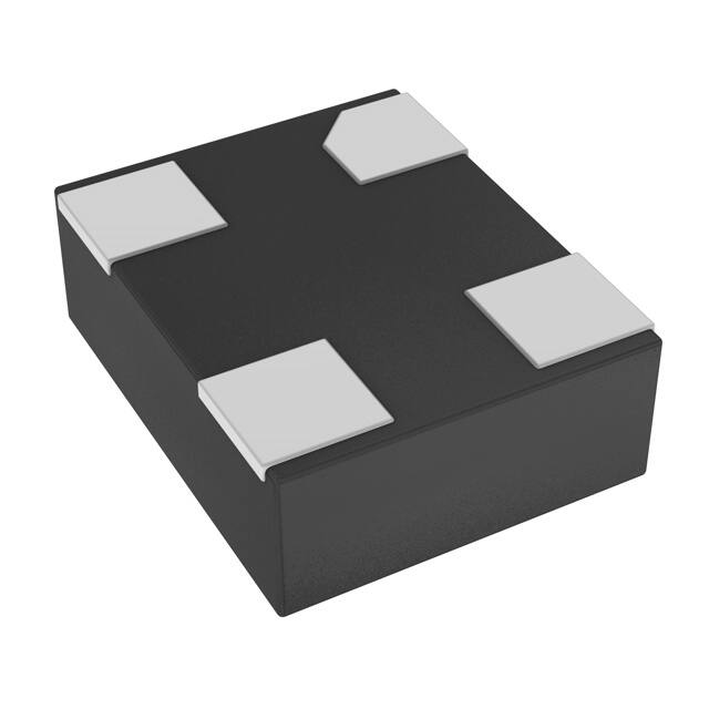
DSC1030
Low-Power CMOS Oscillator
3.0V
Features
General Description
The DSC1030 is a 3.0V fixed frequency MEMS
based PureSilicon™ Oscillator. It can be factory
programmed to any frequency from 1 to
150MHz.
The DSC1030 incorporates an all silicon
resonator that is extremely robust and nearly
immune to stress related fractures, common to
crystal based oscillators. Without sacrificing the
performance and stability required of today’s
systems, a crystal-less design allows for a
higher level of reliability, making the DSC1030
ideal for rugged, industrial, and portable
applications where stress, shock, and vibration
can damage quartz crystal based systems.
Available in industry standard packages, the
DSC1030 can be “dropped-in” to the same PCB
footprint as standard crystal oscillators.
Frequency Range: 1 to 150MHz
Exceptional Stability over Temperature
o ±25 PPM, ±50 PPM
Operating voltage
o 2.7 to 3.3V
Operating Temperature Range
o Industrial -40ºC to 85ºC
o Ext. Commercial -20ºC to 70ºC
o Commercial 0ºC to 70ºC
Low Operating and Standby Current
o 3mA Operating (40MHz)
o 1uA Standby
Ultra Miniature Footprint
o 2.5 x 2.0 x 0.85 mm
o 3.2 x 2.5 x 0.85 mm
o 5.0 x 3.2 x 0.85 mm
o 7.0 x 5.0 x 0.85 mm
Excellent Shock and Vibration
Resistance
Lead Free, RoHS & Reach SVHC
Compliant
Benefits
Block Diagram
VDD
Resonator
Output
VCO
PFD
Applications
Frac-N
PLL
Standby#
(pin1)
Pin for pin “drop in” replacement for
industry standard oscillators
Semiconductor level reliability,
significantly higher than quartz
Short mass production lead-times
Longer Battery Life / Reduced Power
Compact Plastic package
Cost Effective
GND
Mobile Applications
Consumer Electronics
Portable Electronics
CCD Clock for VTR Cameras
Low Profile Applications
Industrial
All Rights Reserved. No part of this document may be copied or reproduced in any form without the prior written permission of Micrel, Inc. Micrel Inc. may update or make changes
to the contents, products, programs or services described at any time without notice. This document neither states nor implies any kind of warranty, including, but not limited to
implied warranties of merchantability or fitness for a particular use.
Page 1
MK-Q-B-P-D-031809-02-7
�3.0V
DSC1030
Low-Power CMOS Oscillator
Absolute Maximum Ratings1
Item
Min.
Max
Unit
Input Voltage
-0.3
VDD+0.3
V
Junction Temp
-
+150
°C
Storage Temp
-55
+150
°C
Soldering Temp
-
+260
°C
ESD
-
DSC1030
Condition
2000
200
CDM
500
-
032.0000
T
Family
Package, Temp
& Stability
40 sec max.
Tape/
Reel
Output Freq
1.0 to 150MHz
V
HBM
MM
CE1
* See Ordering Information for details
Ordering Code
Recommended Operating Conditions
Parameter
Symbol
Range
Supply Voltage
VDD
2.7 to 3.3V
Output Load
ZL
R>10KΩ, C≤15pF
T
-40 − +85 °C
-20 − +70 °C
0 − +70 °C
Operating Temperature
Option 1
Option 2
Option 3
Specifications
Parameter
Frequency
Frequency Tolerance
Option 1
Option 2
Option 3
Supply Current, no load
Supply Current, standby
Symbol
Condition
Min.
f0
Single Frequency
1
Δf
IDD
-40°C to +85°C
-20°C to +70°C
0°C to +70°C
CL=0p
1 to 40MHz
RL=∞
40 to 80MHz
T=25°
80 to 125MHz
C
125 to 150MHz
IDD
T=25°C
VOH
VOL
CL=15pF
tR
tF
CL=15pF; T=25°C
20%/80%*VDD
Output Startup Time2
tSU
T=25°C
Output Disable Time
tDA
Output Logic Levels
Output logic high
Output logic low
Output Transition time
Rise Time
Fall Time
Typ.
Max.
Unit
150
MHz
±25,±50
±25,±50
±25,±50
3
4
5
6
10
ppm
mA
1.0
uA
0.2*VDD
Volts
1.3
1.3
2
2
ns
1.5
3
ms
20
100
ns
0.8*VDD
-
Output Duty Cycle
SYM
45
55
%
Input Logic Levels
Input logic high
Input logic low
VIH
VIL
0.75*VDD
-
0.25* VDD
Volts
Jitter, Cycle to Cycle
JCC
F = 100MHz3
95
ps
Notes:
1.
Absolute maximum ratings are those values beyond which the safety of the device cannot be guaranteed. The device should not be
operated beyond these limits.
2.
tSU is time to stable output frequency after VDD is applied. tSU and tEN (after EN is asserted) are identical values.
3.
See typical cycle to cycle jitter graph for frequency dependence.
All Rights Reserved. No part of this document may be copied or reproduced in any form without the prior written permission of Micrel, Inc. Micrel Inc. may update or make changes
to the contents, products, programs or services described at any time without notice. This document neither states nor implies any kind of warranty, including, but not limited to
implied warranties of merchantability or fitness for a particular use.
Page 2
MK-Q-B-P-D-031809-02-7
�3.0V
DSC1030
Low-Power CMOS Oscillator
Nominal Performance Characteristics
3.0V Characteristics
Standby Current
Supply Current
1
Ta = 25°C
1pF
8pF
15pF
Standby Current (µA)
Supply Current (mA)
16
12
8
4
0
-40°C
0.8
0.6
0.4
0.2
50
100
Frequency (MHz)
150
0
Rise Time
50
100
Frequency (MHz)
150
Fall Time
2
2
-40°C
25°C
85°C
-40°C
1.5
Fall Time (ns)
Rise Time (ns)
85°C
0
0
1
0.5
0
25°C
85°C
1.5
1
0.5
0
0
50
100
Frequency (MHz)
150
0
Period Jitter
50
100
Frequency (MHz)
150
Cycle to Cycle Jitter
40
200
25°C
25°C
30
150
Jitter (ps)
RMS Jitter (ps)
25°C
20
10
100
50
0
0
0
50
100
Frequency (MHz)
150
0
50
100
Frequency (MHz)
150
All Rights Reserved. No part of this document may be copied or reproduced in any form without the prior written permission of Micrel, Inc. Micrel Inc. may update or make changes to
the contents, products, programs or services described at any time without notice. This document neither states nor implies any kind of warranty, including, but not limited to implied
warranties of merchantability or fitness for a particular use.
Page 3
MK-Q-B-P-D-031809-02-7
�3.0V
DSC1030
Low-Power CMOS Oscillator
Output Waveform
tR
tF
VOH
Output
VOL
tEN
1/fo
tDA
VIH
Standby#
VIL
Standby Function
Standby#
Output
(pin 1)
(pin 3)
Hi Level
Output ON
Open
(no connect)
Output ON
Low Level
High Impedance
Test Circuit
IDD
VDD
0.01uF
4
3
1
2
15pF
*VSD
*VSD = Standby# Logic Level Input
All Rights Reserved. No part of this document may be copied or reproduced in any form without the prior written permission of Micrel, Inc. Micrel Inc. may update or make changes
to the contents, products, programs or services described at any time without notice. This document neither states nor implies any kind of warranty, including, but not limited to
implied warranties of merchantability or fitness for a particular use.
Page 4
MK-Q-B-P-D-031809-02-7
�3.0V
DSC1030
Low-Power CMOS Oscillator
Board Layout (recommended)
Solder Reflow Profile
20-40
Sec
MSL 1 @ 260°C refer to JSTD-020C
Ramp-Up Rate (200°C to Peak Temp) 3°C/Sec Max.
Preheat Time 150°C to 200°C
60-180 Sec
Time maintained above 217°C
60-150 Sec
255-260°C
Peak Temperature
Time within 5°C of actual Peak
20-40 Sec
6°C/Sec Max.
Ramp-Down Rate
Time 25°C to Peak Temperature
8 min Max.
Se
3C
/
217°C
200°C
60-150
Sec
S
6C/
ec
3C
/
Se
cM
ax
.
Reflow
25°C
60-180
Sec
x.
150°C
Ma
Temperature (°C)
cM
ax
.
260°C
Cool
Pre heat
Time
8 min max
Package Dimensions
7.0 x 5.0 mm Plastic Package
External Dimensions
7.0±0.10 [0.276±0.004]
#4
Recommended Land Pattern*
5.08 [0.200]
5.08 [0.2]
#3
#4
#3
2.6 [0.102]
2.6 [0.102]
3.5 [0.138]
0.2 [0.008]
2.2 [0.087]
#1
#2
5.0±0.10 [0.197±0.004]
#2
1.4 [0.055]
0.2 [0.008]
#1
0.85±0.05 [0.033±0.002]
o
o
o
o
o
1.4 [0.055]
0.2 [0.008]
1.4 [0.055]
1.2 [0.047]
No.
1
2
3
4
o
Pin Terminal
Standby#
GND
Output
VDD
*Note: The center pad is not connected
internally and should be left unconnected or tied to GND.
units: mm [inch]
All Rights Reserved. No part of this document may be copied or reproduced in any form without the prior written permission of Micrel, Inc. Micrel Inc. may update or make changes
to the contents, products, programs or services described at any time without notice. This document neither states nor implies any kind of warranty, including, but not limited to
implied warranties of merchantability or fitness for a particular use.
Page 5
MK-Q-B-P-D-031809-02-7
�3.0V
DSC1030
Low-Power CMOS Oscillator
5.0 x 3.2 mm Plastic Package
External Dimensions
2.54 [0.100]
2.54 [0.100]
5±0.10 [0.197±0.004]
#4
Recommended Land Pattern
#3
2.1 [0.083]
#4
#3
1.2 [0.047]
0.2 [0.008]
0.1 [0.004]
#2
1.2 [0.047]
#1
#2
3.2±0.10 [0.126±0.004]
1.1 [0.043]
#1
0.1 [0.004]
1.2 [0.047]
0.9 [0.035]
No.
1
2
3
4
0.85±0.05 [0.033±0.002]
Pin Terminal
Standby#
GND
Output
VDD
units: mm [inch]
3.2 x 2.5 mm Plastic Package
Recommended Land Pattern
External Dimensions
3.2±0.05 [0.126±0.002]
#4
2.1 [0.083]
2.1 [0.083]
#3
#3
#4
0.9 [0.035]
0.9 [.035]
1.0 [0.039]
CO.25
#1
#2
2.5±0.05 [0.098±0.002]
#2
0.9±0.05 [0.035±0.002]
#1
0.8±0.1 [0.031±0.004]
0.85±0.05 [0.033±0.002]
No
.1
2
3
4
Pin Terminal
Standby#
GND
Output
VDD
0.2 [0.008]
0.9 [0.035]
units: mm [inch]
All Rights Reserved. No part of this document may be copied or reproduced in any form without the prior written permission of Micrel, Inc. Micrel Inc. may update or make changes
to the contents, products, programs or services described at any time without notice. This document neither states nor implies any kind of warranty, including, but not limited to
implied warranties of merchantability or fitness for a particular use.
Page 6
MK-Q-B-P-D-031809-02-7
�3.0V
DSC1030
Low-Power CMOS Oscillator
2.5 x 2.0 mm Plastic Package
External Dimensions
2.5±0.05 [0.098±0.002]
#4
Recommended Land Pattern
1.65 [0.065]
1.65 [0.065]
#3
#3
#4
0.7 [0.028]
0.7 [0.028]
0.85 [0.033]
CO.25
#1
#2
0.65±0.05 [0.026±0.002]
#2
2.0±0.05 [0.079±0.002]
#1
0.2 [0.008]
0.65 [0.026]
0.65±0.10 [0.026±0.004]
No
.1
2
3
4
0.85±0.05 [0.033±0.002]
Pin Terminal
Standby#
GND
Output
VDD
units: mm [inch]
Ordering Information
DSC1030 PTS – xxx.xxxx T
PART NUMBERING GUIDE
Package
(Plastic QFN)
P=A:
P=B:
P=C:
P=D:
7.0x5.0mm
5.0x3.2mm
3.2x2.5mm
2.5x2.0mm
Temperature
Stability
Frequency
Packing Option
T=C:
0o ~ +70o C
T=E: -20o ~ +70o C
T=I: -40o ~ +85o C
S=1: ±50ppm
S=2: ±25ppm
(4 decimal places)
-
XXX.XXXX
Blank: Tubes
T: Tape & Reel
Example: DSC1030CE1–123.0000T
The example part number above is a 123.0000MHz oscillator in Plastic 3.2x2.5mm package, with ±50ppm
stability over an operating temperature of -20 to +70oC, shipped in Tape and Reel. The reel size (7” or 13”
diameter) will be determined by the factory based on quantity.
Disclaimer:
Micrel makes no representations or warranties with respect to the accuracy or completeness of the information furnished in this data sheet. This information is not intended as a
warranty and Micrel does not assume responsibility for its use. Micrel reserves the right to change circuitry, specifications and descriptions at any time without notice. No
license, whether express, implied, arising by estoppel or otherwise, to any intellectual property rights is granted by this document. Except as provided in Micrel’s terms and
conditions of sale for such products, Micrel assumes no liability whatsoever, and Micrel disclaims any express or implied warranty relating to the sale and/or use of Micrel
products including liability or warranties relating to fitness for a particular purpose, merchantability, or infringement of any patent, copyright or other intellectual property right.
MICREL, Inc.
Phone: +1 (408) 944-0800
●
●
2180 Fortune Drive,
Fax: +1 (408) 474-1000
San Jose, California
95131
● Email: hbwhelp@micrel.com
●
●
USA
www.micrel.com
All Rights Reserved. No part of this document may be copied or reproduced in any form without the prior written permission of Micrel, Inc. Micrel Inc. may update or make changes
to the contents, products, programs or services described at any time without notice. This document neither states nor implies any kind of warranty, including, but not limited to
implied warranties of merchantability or fitness for a particular use.
Page 7
MK-Q-B-P-D-031809-02-7
�


 工商网监
湘ICP备2023018690号
工商网监
湘ICP备2023018690号

