DSC12X1
High Performance CMOS MEMS Oscillator
Features
General Description
• Wide Frequency Range: 2.5 MHz to 170 MHz
(CMOS)
• Very Low RMS Phase Jitter: 650 fs (typ.)
• High Stability: ±20 ppm, ±25 ppm, ±50 ppm
• Wide Temperature Range:
- Automotive: –40°C to +125°C
- Extended Industrial: –40°C to +105°C
- Industrial: –40°C to +85°C
- Commercial: –20°C to +70°C
• Small Industry-Standard Footprints
- 2.5 mm x 2.0 mm
- 3.2 mm x 2.5 mm
- 5.0 mm x 3.2 mm
- 7.0 mm x 5.0 mm
• Excellent Shock and Vibration Immunity
- Qualified to MIL-STD-883
• High Reliability
- 20x Better MTF than Quartz Oscillators
• Supply Range of 2.25V to 3.63V
• Standby, Frequency Select, and Output Enable
Functions
• Lead-Free and RoHS-Compliant
• Contact factory for Automotive-Grade AEC-Q100
Product
The DSC12x1 family of high performance oscillators
utilizes the latest generation of silicon MEMS
technology that improves phase noise and provides
excellent jitter and stability over a wide range of supply
voltages and temperatures. By eliminating the need for
quartz or SAW technology, MEMS oscillators
significantly enhance reliability and accelerate product
development,
while
meeting
stringent
clock
performance criteria for a variety of communications,
storage, and networking applications.
Applications
•
•
•
•
•
Storage Area Networks
Passive Optical Networks
10/100G Ethernet
HD/SD/SDI Video and Surveillance
Display Port
The DSC12x1 family features a control function on
pin 1 or pin 2 that permits either a standby feature
(complete power down when STDBY is low), output
enable (output is tri-stated with OE low), or a frequency
select (choice of two frequencies selected by FS
high/low). See the Product Identification System
section for detailed information.
All oscillators are available in industry-standard
packages, including the small 2.5 mm x 2.0 mm, and
are “drop-in” replacements for standard 4-pin and 6-pin
CMOS quartz crystal oscillators.
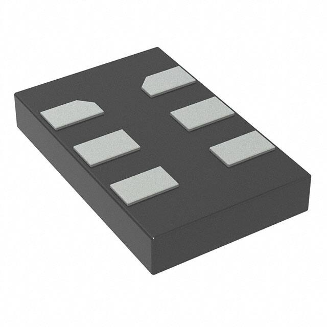
Package Types
DSC1201/1211/1221
6-Lead CDFN/VDFN
OE/STDBY/FS
1
6
VDD
NC
2
5
NC
GND
3
4
CLK
DSC1231/1241/1251
6-Lead CDFN/VDFN
2019 Microchip Technology Inc.
NC
1
6
VDD
OE/STDBY/FS
2
5
NC
GND
3
4
CLK
DS20006010A-page 1
�DSC12X1
Functional Block Diagrams
DSC1201/1211/1221
Pin 1
OE/STDBY/FS
Pin 2
NC
Pin 3
GND
SUPPLY
REGULATION
DIGITAL
CONTROL
Pin 6
VDD
Pin 5
NC
MEMS
RESONATOR
TEMP SENSOR +
CONTROL &
COMPENSATION
PLL
OUTPUT
DIV
Pin 4
CLK
DSC1231/1241/1251
Pin 1
NC
Pin 2
OE/STDBY/FS
Pin 3
GND
DS20006010A-page 2
SUPPLY
REGULATION
DIGITAL
CONTROL
Pin 5
NC
MEMS
RESONATOR
TEMP SENSOR +
CONTROL &
COMPENSATION
Pin 6
VDD
PLL
OUTPUT
DIV
Pin 4
CLK+
2019 Microchip Technology Inc.
�DSC12X1
1.0
ELECTRICAL CHARACTERISTICS
Absolute Maximum Ratings †
Supply Voltage .......................................................................................................................................... –0.3V to +4.0V
Input Voltage .....................................................................................................................................–0.3V to VDD + 0.3V
ESD Protection (HBM) ............................................................................................................................................... 4 kV
ESD Protection (MM) ................................................................................................................................................400V
ESD Protection (CDM) ............................................................................................................................................ 1.5 kV
† Notice: Stresses above those listed under “Absolute Maximum Ratings” may cause permanent damage to the device.
This is a stress rating only and functional operation of the device at those or any other conditions above those indicated
in the operational sections of this specification is not intended. Exposure to maximum rating conditions for extended
periods may affect device reliability.
ELECTRICAL CHARACTERISTICS
Electrical Characteristics: VDD = 2.5V ±10% or 3.3V ±10%; TA = –40°C to +125°C, unless noted.
Parameter
Supply Voltage
Supply Current
Standby Current
Frequency Stability
Startup Time
Symbol
Min.
Typ.
Max.
Units
VDD
2.25
—
3.63
V
—
27
—
—
23
—
—
2.5
5
—
—
±20
—
—
±25
—
—
±50
tSU
—
5.5
6
VIH
0.75 x
VDD
—
—
VIL
—
—
0.25 x
VDD
tDA
—
—
25
ns
Note 3
—
—
6
ms
STDBY
IDD
ISTDBY
∆f
Input Logic Levels
Output Disable Time
Output Enable Time
tEN
Enable Pull-Up Resistor
—
Frequency
mA
µA
ppm
ms
Conditions
Note 1
Output enabled, CMOS (no load),
fOUT = 100 MHz
Output disabled (tri-state),
fOUT = 100 MHz
Input pin = STDBY = Asserted
(VDD = 3.3V)
Includes frequency variations due
to initial tolerance, temp., and
power supply voltage
From 90% VDD to valid clock
output, T = +25°C, Note 2
Input logic high
V
Input logic low
—
—
350
ns
OE
—
1.5
—
MΩ
Pull-up resistor on pin 1, Note 4
f0
2.5
—
170
MHz
—
Output Logic Level High
VOH
0.8 x
VDD
—
—
Output Logic Level Low
VOL
—
—
0.2 x
VDD
—
1.3
—
Standard Drive Strength
—
1.2
—
High Drive Strength
—
1.6
—
—
2.4
—
Output Transition Time, Rise
20% to 80%;CL=15 pF
2019 Microchip Technology Inc.
tR
V
ns
I = ±12 mA (High Drive)
I = ±10 mA (Standard Drive)
I = ±8 mA (Mid Drive)
I = ±6 mA (Low Drive)
Mid Drive Strength
Low Drive Strength
DS20006010A-page 3
�DSC12X1
ELECTRICAL CHARACTERISTICS (CONTINUED)
Electrical Characteristics: VDD = 2.5V ±10% or 3.3V ±10%; TA = –40°C to +125°C, unless noted.
Parameter
Output Transition Time, Fall
20% to 80%;CL=15 pF
Symbol
tF
Min.
Typ.
Max.
—
1.3
—
—
1.1
—
—
1.8
—
Units
Conditions
Standard Drive Strength
ns
High Drive Strength
Mid Drive Strength
—
2.4
—
Output Duty Cycle
SYM
45
—
55
%
—
Low Drive Strength
Period Jitter, Peak-to-Peak
JPTP
—
25
—
ps
fOUT = 100 MHz, High Drive
Cycle-to-Cycle Jitter, Peak
JCC
—
22
—
ps
fOUT = 100 MHz, High Drive
Integrated Phase Noise
(Random)
JPH
—
0.65
—
psRMS
Note 1:
2:
3:
4:
12 kHz to 20 MHz @ 100 MHz, TA
= +105°C
VDD pin should be filtered with a 0.1 µF capacitor.
tSU is the time to 100 ppm stable output frequency after VDD is applied and outputs are enabled.
tDA: See the Output Waveform and the Test Circuit sections for more information.
Output is enabled if pad is floated (not connected).
DS20006010A-page 4
2019 Microchip Technology Inc.
�DSC12X1
TEMPERATURE SPECIFICATIONS
Parameters
Sym.
Min.
Typ.
Max.
Units
Conditions
Maximum Junction Temperature
TJ
—
—
+150
°C
Storage Temperature Range
TS
–55
—
+150
°C
—
Lead Temperature
—
—
—
+260
°C
Soldering, 40s
Temperature Ranges
2019 Microchip Technology Inc.
—
DS20006010A-page 5
�DSC12X1
2.0
PIN DESCRIPTIONS
The descriptions of the pins are listed in Table 2-1 and Table 2-2.
TABLE 2-1:
Pin Number
DSC1201
Pin Name
1
STDBY
2
NC
Description
DSC1221
Description
Pin Name
Standby.
FS
Frequency select.
OE
Output enable.
No connect.
NC
No connect.
NC
No connect.
3
GND
4
CLK
Clock output.
5
NC
No connect.
6
VDD
Pin Number
DSC1211
Pin Name
Power supply
ground.
TABLE 2-2:
2.1
DSC1201/1211/1221 PIN FUNCTION TABLE
Power supply.
Description
GND
Power supply
ground.
GND
Power supply
ground.
CLK
Clock output.
CLK
Clock output.
NC
No connect.
VDD
Power supply.
NC
No connect.
VDD
Power supply.
DSC1231/1241/1251 PIN FUNCTION TABLE
DSC1231
Pin Name
1
NC
2
STDBY
Description
DSC1241
Pin Name
Description
DSC1251
Pin Name
Description
No connect.
NC
No connect.
NC
No connect.
Standby.
FS
Frequency select.
Power supply
ground.
GND
OE
Output enable.
Power supply
ground.
GND
Power supply
ground.
Clock output.
3
GND
4
CLK
Clock output.
CLK
Clock output.
CLK
5
NC
No connect.
NC
No connect.
NC
6
VDD
Power supply.
VDD
Power supply.
VDD
No connect.
Power supply.
Standby
Complete power down when STDBY is low.
2.2
Frequency Select
Two frequencies may be chosen, selected by FS =
High or Low. Please use the ClockWorks tool to
customize frequencies.
2.3
Output Enable
Output buffers (only) are tri-stated when OE is low.
DS20006010A-page 6
2019 Microchip Technology Inc.
�DSC12X1
3.0
TERMINATION SCHEME
VDD
0.1μF
6
2
5
3
4
CL CMOS
Load Capacitance
FIGURE 3-1:
CMOS Termination.
2019 Microchip Technology Inc.
DS20006010A-page 7
�DSC12X1
4.0
OUTPUT WAVEFORM
tR
tF
80%
Output voltage swing.
Refer to table below.
50%
Output
20%
tEN
1/f0
tDA
Enable
VIH
VIL
FIGURE 4-1:
TABLE 4-1:
CMOS Output Waveform.
OUTPUT VOLTAGE SWING BY LOGIC TYPE
Output Logic Protocol
Typical Peak-to-Peak Output Swing
CMOS
VOH, VOL
DS20006010A-page 8
2019 Microchip Technology Inc.
�DSC12X1
5.0
TEST CIRCUIT
IDD
VDD
0.1μF
6
5
4
1
2
3
15pF
VDA
FIGURE 5-1:
CMOS Test Circuit.
2019 Microchip Technology Inc.
DS20006010A-page 9
�DSC12X1
6.0
SOLDER REFLOW PROFILE
FIGURE 6-1:
TABLE 6-1:
Solder Reflow Profile.
SOLDER REFLOW
MSL 1 @ 260°C Refer to JSTD-020C
Ramp-Up Rate (200°C to Peak Temp.)
3°C/sec. max.
Preheat Time 150°C to 200°C
60 to 180 sec.
Time Maintained above 217°C
Peak Temperature
Time within 5°C of Actual Peak
60 to 150 sec.
255°C to 260°C
20 to 40 sec.
Ramp-Down Rate
–6°C/sec. max.
Time 25°C to Peak Temperature
8 minutes max.
DS20006010A-page 10
2019 Microchip Technology Inc.
�DSC12X1
7.0
BOARD LAYOUT (RECOMMENDED)
Via to GND layer
1
6
Supply bypass
capacitor
2
3
5
4
Via to GND layer
FIGURE 7-1:
DSC12x1 Recommended Board Layout.
2019 Microchip Technology Inc.
DS20006010A-page 11
�DSC12X1
8.0
PHASE NOISE
FIGURE 8-1:
DSC12x1 Phase Noise at 25 MHz.
FIGURE 8-2:
DSC12x1 Phase Noise at 125 MHz.
DS20006010A-page 12
2019 Microchip Technology Inc.
�DSC12X1
9.0
PACKAGING INFORMATION
9.1
Package Marking Information
6-Pin CDFN/VDFN*
XXXXXXXX
DCPYYWW
0SSS
Legend: XX...X
Y
YY
WW
SSS
e3
*
Example
125M0000
DCP1723
0421
Product code or customer-specific information
Year code (last digit of calendar year)
Year code (last 2 digits of calendar year)
Week code (week of January 1 is week ‘01’)
Alphanumeric traceability code
Pb-free JEDEC® designator for Matte Tin (Sn)
This package is Pb-free. The Pb-free JEDEC designator ( e3 )
can be found on the outer packaging for this package.
●, ▲, ▼ Pin one index is identified by a dot, delta up, or delta down (triangle
mark).
Note:
In the event the full Microchip part number cannot be marked on one line, it will
be carried over to the next line, thus limiting the number of available
characters for customer-specific information. Package may or may not include
the corporate logo.
Underbar (_) and/or Overbar (⎯) symbol may not be to scale.
2019 Microchip Technology Inc.
DS20006010A-page 13
�DSC12X1
6-Lead VDFN 2.5 mm x 2.0 mm Package Outline and Recommended Land Pattern
6-Lead Very Thin Dual Flatpack No-Leads (J7A) - 2.5x2.0 mm Body [VDFN]
Note:
For the most current package drawings, please see the Microchip Packaging Specification located at
http://www.microchip.com/packaging
D
A
B
N
(DATUM A)
(DATUM B)
E
NOTE 1
2X
0.05 C
1
2X
2
TOP VIEW
0.05 C
0.10 C
C
A
A1
SEATING
PLANE
6X
0.08 C
SIDE VIEW
2X b2
1
2
L2
5X L1
N
4X b1
0.10
0.05
e
C A B
C
BOTTOM VIEW
Microchip Technology Drawing C04-1005A Sheet 1 of 2
DS20006010A-page 14
2019 Microchip Technology Inc.
�DSC12X1
6-Lead Very Thin Dual Flatpack No-Leads (J7A) - 2.5x2.0 mm Body [VDFN]
Note:
For the most current package drawings, please see the Microchip Packaging Specification located at
http://www.microchip.com/packaging
Units
Dimension Limits
Number of Terminals
N
e
Pitch
Overall Height
A
Standoff
A1
Overall Length
D
Overall Width
E
b1
Terminal Width
Terminal Width
b2
Terminal Length
L1
Terminal Length
L2
MILLIMETERS
MAX
NOM
6
0.825 BSC
0.80
0.90
0.85
0.05
0.02
0.00
2.50 BSC
2.00 BSC
0.60
0.70
0.65
0.20
0.25
0.30
0.60
0.70
0.80
0.665
0.865
0.765
MIN
Notes:
1. Pin 1 visual index feature may vary, but must be located within the hatched area.
2. Package is saw singulated
3. Dimensioning and tolerancing per ASME Y14.5M
BSC: Basic Dimension. Theoretically exact value shown without tolerances.
REF: Reference Dimension, usually without tolerance, for information purposes only.
Microchip Technology Drawing C04-1005A Sheet 2 of 2
2019 Microchip Technology Inc.
DS20006010A-page 15
�DSC12X1
6-Lead Very Thin Dual Flatpack No-Leads (J7A) - 2.5x2.0 mm Body [VDFN]
Note:
For the most current package drawings, please see the Microchip Packaging Specification located at
http://www.microchip.com/packaging
X1
X2
2
1
Y
G2 C
6
G1
SILK SCREEN
E
RECOMMENDED LAND PATTERN
Units
Dimension Limits
E
Contact Pitch
X1
Contact Pad Width (X4)
Contact Pad Width (X2)
X2
Contact Pad Length (X6)
Y
Contact Pad Spacing
C
Space Between Contacts (X4)
G1
Space Between Contacts (X3)
G2
MIN
MILLIMETERS
NOM
0.825 BSC
MAX
0.65
0.25
0.85
1.45
0.38
0.60
Notes:
1. Dimensioning and tolerancing per ASME Y14.5M
BSC: Basic Dimension. Theoretically exact value shown without tolerances.
2. For best soldering results, thermal vias, if used, should be filled or tented to avoid solder loss during
reflow process
Microchip Technology Drawing C04-3005A
DS20006010A-page 16
2019 Microchip Technology Inc.
�DSC12X1
6-Lead VDFN 3.2 mm x 2.5 mm Package Outline and Recommended Land Pattern
6-Lead Very Thin Plastic Dual Flatpack No-Lead (H5A) - 3.2x2.5 mm Body [VDFN]
Note:
For the most current package drawings, please see the Microchip Packaging Specification located at
http://www.microchip.com/packaging
D
A
B
N
(DATUM A)
(DATUM B)
E
NOTE 1
2X
0.05 C
1
2X
2
TOP VIEW
0.05 C
0.10 C
C
A1
A
SEATING
PLANE
6X
0.08 C
SIDE VIEW
2X b2
1
2
NOTE 1
L
N
4X b1
L1
e
BOTTOM VIEW
0.07
0.05
C A B
C
Microchip Technology Drawing C04-1007A Sheet 1 of 2
2019 Microchip Technology Inc.
DS20006010A-page 17
�DSC12X1
6-Lead Very Thin Plastic Dual Flatpack No-Lead (H5A) - 3.2x2.5 mm Body [VDFN]
Note:
For the most current package drawings, please see the Microchip Packaging Specification located at
http://www.microchip.com/packaging
Units
Dimension Limits
N
Number of Terminals
e
Pitch
A
Overall Height
Standoff
A1
Overall Length
D
E
Overall Width
b1
Terminal Width
b2
Terminal Width
L
Terminal Length
Terminal Pullback
L1
MIN
0.80
0.00
0.85
0.45
0.65
MILLIMETERS
NOM
6
1.05 BSC
0.85
0.02
3.20 BSC
2.50 BSC
0.90
0.50
0.70
0.10 REF
MAX
0.90
0.05
0.95
0.55
0.75
Notes:
1. Pin 1 visual index feature may vary, but must be located within the hatched area.
2. Package is saw singulated
3. Dimensioning and tolerancing per ASME Y14.5M
BSC: Basic Dimension. Theoretically exact value shown without tolerances.
REF: Reference Dimension, usually without tolerance, for information purposes only.
Microchip Technology Drawing C04-1007A Sheet 2 of 2
DS20006010A-page 18
2019 Microchip Technology Inc.
�DSC12X1
6-Lead Very Thin Plastic Dual Flatpack No-Lead (H5A) - 3.2x2.5 mm Body [VDFN]
Note:
For the most current package drawings, please see the Microchip Packaging Specification located at
http://www.microchip.com/packaging
X2
G
6
C
Y
1
2
X1
SILK SCREEN
E
RECOMMENDED LAND PATTERN
Units
Dimension Limits
Contact Pitch
E
Contact Pad Spacing
C
Contact Pad Width (X4)
X1
Contact Pad Width (X2)
X2
Contact Pad Length (X6)
Y
Space Between Contacts (X4)
G1
MIN
MILLIMETERS
NOM
1.05 BSC
1.60
MAX
1.00
0.60
0.85
0.25
Notes:
1. Dimensioning and tolerancing per ASME Y14.5M
BSC: Basic Dimension. Theoretically exact value shown without tolerances.
Microchip Technology Drawing C04-3007A
2019 Microchip Technology Inc.
DS20006010A-page 19
�DSC12X1
6-Lead CDFN 5.0 mm x 3.2 mm Package Outline and Recommended Land Pattern
DS20006010A-page 20
2019 Microchip Technology Inc.
�DSC12X1
6-Lead VDFN 7.0 mm x 5.0 mm Package Outline and Recommended Land Pattern
��/HDG�9HU\�7KLQ�'XDO�)ODWSDFN��1R�/HDG�3DFNDJH��+3$�����[��PP�%RG\�>9')1@
1RWH�
)RU�WKH�PRVW�FXUUHQW�SDFNDJH�GUDZLQJV��SOHDVH�VHH�WKH�0LFURFKLS�3DFNDJLQJ�6SHFLILFDWLRQ�ORFDWHG�DW
KWWS���ZZZ�PLFURFKLS�FRP�SDFNDJLQJ
'
$
%
1
�'$780�$�
�'$780�%�
(
127(��
�;
���� &
�
�
�;
���� &
723�9,(:
6($7,1*
3/$1(
$�
���� &
&
$
�;
���� &
6,'(�9,(:
�
�
127(��
�/��
/
1
�;�E
H
%27720�9,(:
����
����
& $ %
&
0LFURFKLS�7HFKQRORJ\�'UDZLQJ��&��������5HY�$�6KHHW���RI��
2019 Microchip Technology Inc.
DS20006010A-page 21
�DSC12X1
��/HDG�9HU\�7KLQ�'XDO�)ODWSDFN��1R�/HDG�3DFNDJH��+3$�����[��PP�%RG\�>9')1@
1RWH�
)RU�WKH�PRVW�FXUUHQW�SDFNDJH�GUDZLQJV��SOHDVH�VHH�WKH�0LFURFKLS�3DFNDJLQJ�6SHFLILFDWLRQ�ORFDWHG�DW
KWWS���ZZZ�PLFURFKLS�FRP�SDFNDJLQJ
1XPEHU�RI�7HUPLQDOV
3LWFK
2YHUDOO�+HLJKW
6WDQGRII
2YHUDOO�/HQJWK
2YHUDOO�:LGWK
7HUPLQDO�:LGWK
7HUPLQDO�/HQJWK
3XOOEDFN
8QLWV
'LPHQVLRQ�/LPLWV
1
H
$
$�
'
(
E
/
/�
0,1
����
����
����
����
0,//,0(7(56
120
�
�����%6&
����
����
�����%6&
�����%6&
����
����
�����5()
0$;
����
����
����
����
Notes:
�� 3LQ���YLVXDO�LQGH[�IHDWXUH�PD\�YDU\��EXW�PXVW�EH�ORFDWHG�ZLWKLQ�WKH�KDWFKHG�DUHD�
�� 3DFNDJH�LV�VDZ�VLQJXODWHG
�� 'LPHQVLRQLQJ�DQG�WROHUDQFLQJ�SHU�$60(�9')1@
1RWH�
)RU�WKH�PRVW�FXUUHQW�SDFNDJH�GUDZLQJV��SOHDVH�VHH�WKH�0LFURFKLS�3DFNDJLQJ�6SHFLILFDWLRQ�ORFDWHG�DW
KWWS���ZZZ�PLFURFKLS�FRP�SDFNDJLQJ
�
&


 工商网监
湘ICP备2023018690号
工商网监
湘ICP备2023018690号
