DSC557-03
Two Output PCIe Gen1/2/3/4 Clock Generator
Features
General Description
• Complies with PCIe Gen1/2/3/4 Common Clock
Spec
• Integrated MEMS Resonator Eliminates the Need
for External 25 MHz Crystal
• 100 MHz HCSL/LVDS/LVCMOS Options
Available
• Wide Temperature Range:
- Ext. Industrial: –40°C to +105°C
- Industrial:
–40°C to +85°C
- Commercial: –20°C to +70°C
• Supply Range of 2.25V to 3.6V
• Low Power Consumption
- 30% Lower than Competing Devices
• Excellent Shock & Vibration Immunity
- Qualified to MIL-STD-883
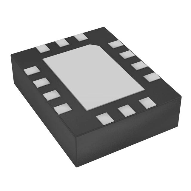
• Space Saving 14-Lead QFN Package
• Lead-Free and RoHS-Compliant
The DSC557-03 is a two output PCI express clock
generator meeting Gen1, Gen2, Gen3 and Gen 4
specifications. The clock generator uses proven silicon
MEMS technology to provide 100 MHz* differential
output clocks with excellent jitter and stability over a
wide range of supply voltages and temperatures. By
eliminating the external quartz crystal, the DSC557-03
significantly enhances reliability and accelerates
product development, while meeting stringent clock
performance criteria for a variety of communications,
storage, and networking applications.
Applications
• Communications/Networking
- Ethernet
- 1G, 10GBASE-T/KR/LR/SR, and FcoE
- Routers and Switches
- Gateways, VoIP, Wireless AP’s
- Passive Optical Networks
• Storage
- SAN, NAS, SSD, JBOD
• Embedded Applications
- Industrial, Medical, and Avionics
- Security Systems and Office Automation
- Digital Signage, POS and others
• Consumer Electronics
- Smart TV, Bluray, STB
2020 Microchip Technology Inc.
DSC557-03 has an Output Enable / Disable feature
allowing it to disable the outputs when OE is low. The
device is available in a space saving 14 pin QFN.
Additional output formats are also available in any
combination of LVCMOS, LVDS, and HCSL.
Block Diagram
Control Circuitry
MEMS
OE
PLL
Output
Control
and
Divider
CLK0+
CLK0-
CLK1CLK1+
DS20006318A-page 1
�DSC557-03
Package Type
Connection Diagram
14 Pin QFN
Two HCSL Outputs)
OE
VDD0
14
13
VDD1
NC
Pin Diagram
14 Pin QFN
3.2 mm x 2.5 mm
0.01 uF
12
1
14
11
CLK0+
NC
2
10
CLK0-
NC
3
9
CLK1-
VSS
4
8
CLK1+
TABLE 0-1:
12
1
11
2
10
3
9
4
8
5
6
7
CLK0+
CLK050 :
50 :
CLK1-
Ropt
7
CLK1+
Ropt 22:��� 33 :�optional
NC
6
NC
NC
5
+
Enable
-
13
+
VDD
-
0.01 uF
50 :
50 :
PIN DESCRIPTION (14 QFN)
Pin Number
Pin Name
Pin Type
1
OE
I
Description
Output Enable; Active-high.
2
NC
N/A
Ground recommended or leave as a NC.
3
NC
N/A
Ground recommended or leave as a NC.
4
VSS
Power
5
NC
N/A
Ground.
Ground recommended or leave as a NC.
6
NC
N/A
Ground recommended or leave as a NC.
7
NC
N/A
Ground recommended or leave as a NC.
8
CLK1+
O
True output of differential pair.
9
CLK1–
O
Complement output of differential pair.
10
CLK0–
O
Complement output of differential pair.
11
CLK0+
O
True output of differential pair.
12
VDD1
Power
Power Supply for Output 1 (CLK1+/–).
13
VDD0
Power
Power Supply for Core and Output 0 (CLK0+/–).
14
NC
N/A
Ground recommended or leave as a NC.
ePAD
ePAD
N/A
Thermal pad, floating, not DC connected to substrate
ground.
DS20006318A-page 2
2020 Microchip Technology Inc.
�DSC557-03
1.0
ELECTRICAL CHARACTERISTICS
Absolute Maximum Ratings †
Supply Voltage .......................................................................................................................................... –0.3V to +4.0V
Input Voltage .................................................................................................................................... –0.3V to VDD + 0.3V
ESD Protection (HBM) ...............................................................................................................................................4 kV
ESD Protection (MM) ................................................................................................................................................400V
ESD Protection (CDM) ............................................................................................................................................1.5 kV
† Notice: Stresses above those listed under “Absolute Maximum Ratings” may cause permanent damage to the device.
This is a stress rating only and functional operation of the device at those or any other conditions above those indicated
in the operational sections of this specification is not intended. Exposure to maximum rating conditions for extended
periods may affect device reliability.
ELECTRICAL CHARACTERISTICS
Electrical Characteristics: VDD = 3.3V; T = 25°C, unless specified otherwise.
Parameter
Symbol
Min.
Typ.
Max.
Units
Conditions
Supply Voltage
VDD
2.25
—
3.6
V
Note 1
Supply Current
IDD
—
—
—
—
EN pin low - outputs are disabled
Supply Current (Two HCSL
Outputs), Note 2
IDD
—
60
—
mA
EN pin high - outputs are enabled
RL = 50Ω, FO1 = FO2 = 100 MHz
—
—
±100
Frequency Stability
Δf
ppm
Includes frequency variations due
to initial tolerance, temp. and power
supply voltage
Startup Time
—
—
±50
tSU
—
—
5
VIH
0.7 x
VDD
—
—
VIL
—
—
0.3 x
VDD
Output Disable Time
tDA
—
—
5
ns
Note 4
Output Enable Time
tEN
—
—
20
ns
—
Pull-Up Resistor
—
—
40
—
kΩ
Pull-up on OE pin
Output Logic High
VOH
0.725
—
—
V
Output Logic Low
VOL
—
—
0.1
V
—
—
750
—
mV
Single-ended
Rise Time
tR
200
—
400
Fall Time
tF
200
—
400
ps
20% to 80%, RL = 50Ω, CL = 2 pF
Frequency
f0
—
100
—
Output Duty Cycle
SYM
48
—
52
Period Jitter Note 5
JPER
—
2.5
—
Input Logic Levels,
ms
Note 3
Input logic high
V
Input logic low
HCSL Outputs
Output Logic Levels
Peak to Peak Output Swing
RL = 50Ω
Output Transition Time
2020 Microchip Technology Inc.
MHz
%
Single frequency
Differential
psRMS FO1 = FO2 = 100 MHz
DS20006318A-page 3
�DSC557-03
ELECTRICAL CHARACTERISTICS (CONTINUED)
Electrical Characteristics: VDD = 3.3V; T = 25°C, unless specified otherwise.
Parameter
Jitter, Phase
(Common Clock Architecture)
Note 6
Symbol
Min.
Typ.
Max.
Units
Conditions
TJ
—
17
86
psPP
PCIe Gen 1.1
TJ = DJ + 14.069 x RJ (BER 10-12)
JRMS-CCHF
—
1.46
3.1
psRMS PCIe Gen 2.1, 1.5 MHz to Nyquist
JRMS-CCLF
—
0.08
3.0
psRMS PCIe Gen 2.1, 10 kHz to 1.5 MHz
—
0.313
1.0
psRMS PCIe Gen 3.0
—
0.313
0.5
psRMS PCIe Gen 4.0
JRMS-DCHF
—
2.15
—
psRMS PCIe Gen 2.1, 1.5 MHz to Nyquist
JRMS-CCLF
—
0.06
—
psRMS PCIe Gen 2.1, 10 kHz to 1.5 MHz
JRMS-DC
—
0.32
—
psRMS PCIe Gen 3.0
JRMS-CC
Integrated Phase Noise
(Data Clock Architecture)
Note 6
LVDS Output
Offset Voltage
VOS
1.125
1.25
1.40
V
ΔVOS
—
—
50
mV
—
Output High Voltage
VOH
0.9xVDD
—
—
V
—
Output Low Voltage
VOL
—
—
0.1xVDD
V
—
Output Frequency
fOUT
—
100
—
MHz
—
Differential Output Voltage
VOD
275
350
475
mVPP
—
ΔVOD
—
—
40
mV
—
tr/tf
—
200
—
ps
20% – 80%
Output Duty Cycle
ODC
48
50
52
%
20% – 80%, RL = 50Ω, CL = 2 pF
Period Jitter, Peak to Peak
JPTP
—
2.5
—
ps
fOUT = 100 MHz, Standard Drive
—
0.28
—
—
0.4
—
—
1.7
2.0
VOH
0.8xVDD
—
—
Output Low Voltage
VOL
—
—
Output Frequency
fOUT
—
100
VOS Magnitude Change
VOD Magnitude Change
LVDS Output Rise/Fall Time
Integrated Phase Noise
JPH
psRMS
VDD = 2.5V/3.3V
200 kHz to 20 MHz @ 100 MHz,
TA = +105°C
100 kHz to 80 MHz @ 100 MHz
12 kHz to 10 MHz @ 100 MHz
LVCMOS Output
Output High Voltage
Output Rise/Fall Time
V
±10 mA drive current
0.2xVDD
V
±10 mA drive current
—
MHz
—
tr/tf
—
1.2
—
ns
20% – 80%, CL = 15 pF
Output Duty Cycle
ODC
48
50
52
%
fOUT = 100 MHz, Standard Drive
Period Jitter
JPTP
—
3
—
psRMS fOUT = 100 MHz, Standard Drive
—
0.3
—
200 kHz to 20 MHz @ 100 MHz
—
0.38
—
psRMS 100 kHz to 20 MHz @ 100 MHz
—
1.7
2.0
Integrated Phase Noise
Note 1:
2:
3:
4:
5:
6:
JPH
12 kHz to 20 MHz @ 100 MHz
VDD pin should be filtered with a 0.1 μF capacitor.
Output is enabled if OE pin is floated or not connected.
tsu is time to 100 PPM stable output frequency after VDD is applied and outputs are enabled.
Output Waveform and Connection Diagram define the parameters.
Period Jitter includes crosstalk from adjacent output.
Jitter limits established by Gen 1.1, Gen 2.1, Gen 3.0 and Gen 4.0 PCIe standards.
DS20006318A-page 4
2020 Microchip Technology Inc.
�DSC557-03
TEMPERATURE SPECIFICATIONS (Note 1)
Parameters
Symbol
Min.
Typ.
Max.
Units
Conditions
Junction Operating Temperature
TJ
—
—
+150
°C
Storage Temperature Range
TS
–55
—
+150
°C
—
Lead Temperature
—
—
+260
—
°C
Soldering, 40s
Temperature Ranges
Note 1:
—
The maximum allowable power dissipation is a function of ambient temperature, the maximum allowable
junction temperature and the thermal resistance from junction to air (i.e., TA, TJ, JA). Exceeding the
maximum allowable power dissipation will cause the device operating junction temperature to exceed the
maximum +150°C rating. Sustained junction temperatures above +150°C can impact the device reliability.
2020 Microchip Technology Inc.
DS20006318A-page 5
�DSC557-03
2.0
OE FUNCTION AND OUTPUT WAVEFORM: HCSL
FIGURE 2-1:
DS20006318A-page 6
OE Function and Output Waveform.
2020 Microchip Technology Inc.
�DSC557-03
3.0
SOLDER REFLOW PROFILE
FIGURE 3-1:
TABLE 3-1:
Solder Reflow Profile.
SOLDER REFLOW
14 QFN MSL 1 @ 260°C refer to JSTD-020C
Ramp-Up Rate (200°C to Peak Temp.)
3°C/sec. max.
Preheat Time 150°C to 200°C
60 to 180 sec.
Time Maintained above 217°C
60 to 150 sec.
Peak Temperature
Time within 5°C of Actual Peak
255°C to 260°C
20 to 40 sec.
Ramp-Down Rate
6°C/sec. max.
Time 25°C to Peak Temperature
8 minutes max.
2020 Microchip Technology Inc.
DS20006318A-page 7
�DSC557-03
4.0
PACKAGING INFORMATION
4.1
Package Marking Information
14-Lead QFN*
(2.5 mm x 3.2 mm)
XXXXXXXXX
DCPYYWW
0SSS
Legend: XX...X
Y
YY
WW
NNN
e3
*
Example
DSC557-03
DCP1924
0K63
Product code or customer-specific information
Year code (last digit of calendar year)
Year code (last 2 digits of calendar year)
Week code (week of January 1 is week ‘01’)
Alphanumeric traceability code
Pb-free JEDEC® designator for Matte Tin (Sn)
This package is Pb-free. The Pb-free JEDEC designator ( e3 )
can be found on the outer packaging for this package.
●, ▲, ▼ Pin one index is identified by a dot, delta up, or delta down (triangle
mark).
Note:
In the event the full Microchip part number cannot be marked on one line, it will
be carried over to the next line, thus limiting the number of available
characters for customer-specific information. Package may or may not include
the corporate logo.
Underbar (_) and/or Overbar (‾) symbol may not be to scale.
DS20006318A-page 8
2020 Microchip Technology Inc.
�DSC557-03
14-Lead QFN Package Outline and Recommended Land Pattern
Note:
For the most current package drawings, please see the Microchip Packaging Specification located at
http://www.microchip.com/packaging.
2020 Microchip Technology Inc.
DS20006318A-page 9
�DSC557-03
NOTES:
DS20006318A-page 10
2020 Microchip Technology Inc.
�DSC557-03
APPENDIX A:
REVISION HISTORY
Revision A (June 2020)
• Conversion of Discera Data Sheet DSC557-03 as
Microchip data sheet DS20006318A.
• Added LVDS section to the Section 1.0 “Electrical Characteristics” table.
• Added LVCMOS section to the Section 1.0
“Electrical Characteristics” table.
2020 Microchip Technology Inc.
DS20006318A-page 11
�DSC557-03
NOTES:
DS20006318A-page 12
2020 Microchip Technology Inc.
�DSC557-03
PRODUCT IDENTIFICATION SYSTEM
To order or obtain information, e.g., on pricing or delivery, contact your local Microchip representative or sales office.
X
PART NO.
Device
Device:
X
X
CLK1 Output
Format
CLK0 Output
Format
Package
X
X
X
Temperature
Frequency
Stability
Media
Type
DSC557-03: Two Output PCIe Gen1/2/3/4 Clock Generator
Examples:
1
CLK1 Output Format 3
4
=
=
=
LVCMOS
LVDS
HCSL
a) DSC557-0313FL0:
CLK1 Output LVCMOS, CLK0
Output LVDS, 14-Lead QFN,
–40°C to +105°C, ±100 ppm, 110/
Tube
1
CLK0 Output Format 3
4
=
=
=
LVCMOS
LVDS
HCSL
b) DSC557-0344FI0:
CLK1 Output HCSL, CLK0 Output
HCSL,14-Lead QFN,
–40°C to +85°C, ±100 ppm, 110/
Tube
Package:
F
=
14-Lead 2.5 mm x 3.2 mm QFN
d) DSC557-0343F
Temperature:
E
I
L
=
=
=
–20°C to +70°C (Commercial)
–40°C to +85°C (Industrial)
–40°C to +105°C (Extended Industrial)
CLK1 Output HCSL, CLK0 Output
LVDS, 14-Lead QFN,
–20°C to +70°C, ±50 ppm,
1,000Tape/Reel
e) DSC557-0343FL1T:
CLK1 Output HCSL, CLK0 Output
LVDS, 14-Lead QFN,
40°C to +105°C, ±50 ppm,
1,000Tape/Reel
Frequency
Stability:
0
1
=
=
±100 ppm
±50 ppm
Media Type:
=
T
=
Note 1:
110/Tube
1,000/Reel
2020 Microchip Technology Inc.
Tape and Reel identifier only appears in the
catalog part number description. This identifier is
used for ordering purposes and is not printed on
the device package. Check with your Microchip
Sales Office for package availability with the
Tape and Reel option.
DS20006318A-page 13
�DSC557-03
NOTES:
DS20006318A-page 14
2020 Microchip Technology Inc.
�Note the following details of the code protection feature on Microchip devices:
•
Microchip products meet the specification contained in their particular Microchip Data Sheet.
•
Microchip believes that its family of products is one of the most secure families of its kind on the market today, when used in the
intended manner and under normal conditions.
•
There are dishonest and possibly illegal methods used to breach the code protection feature. All of these methods, to our
knowledge, require using the Microchip products in a manner outside the operating specifications contained in Microchip’s Data
Sheets. Most likely, the person doing so is engaged in theft of intellectual property.
•
Microchip is willing to work with the customer who is concerned about the integrity of their code.
•
Neither Microchip nor any other semiconductor manufacturer can guarantee the security of their code. Code protection does not
mean that we are guaranteeing the product as “unbreakable.”
Code protection is constantly evolving. We at Microchip are committed to continuously improving the code protection features of our
products. Attempts to break Microchip’s code protection feature may be a violation of the Digital Millennium Copyright Act. If such acts
allow unauthorized access to your software or other copyrighted work, you may have a right to sue for relief under that Act.
Information contained in this publication regarding device
applications and the like is provided only for your convenience
and may be superseded by updates. It is your responsibility to
ensure that your application meets with your specifications.
MICROCHIP MAKES NO REPRESENTATIONS OR
WARRANTIES OF ANY KIND WHETHER EXPRESS OR
IMPLIED, WRITTEN OR ORAL, STATUTORY OR
OTHERWISE, RELATED TO THE INFORMATION,
INCLUDING BUT NOT LIMITED TO ITS CONDITION,
QUALITY, PERFORMANCE, MERCHANTABILITY OR
FITNESS FOR PURPOSE. Microchip disclaims all liability
arising from this information and its use. Use of Microchip
devices in life support and/or safety applications is entirely at
the buyer’s risk, and the buyer agrees to defend, indemnify and
hold harmless Microchip from any and all damages, claims,
suits, or expenses resulting from such use. No licenses are
conveyed, implicitly or otherwise, under any Microchip
intellectual property rights unless otherwise stated.
Trademarks
The Microchip name and logo, the Microchip logo, Adaptec,
AnyRate, AVR, AVR logo, AVR Freaks, BesTime, BitCloud, chipKIT,
chipKIT logo, CryptoMemory, CryptoRF, dsPIC, FlashFlex,
flexPWR, HELDO, IGLOO, JukeBlox, KeeLoq, Kleer, LANCheck,
LinkMD, maXStylus, maXTouch, MediaLB, megaAVR, Microsemi,
Microsemi logo, MOST, MOST logo, MPLAB, OptoLyzer,
PackeTime, PIC, picoPower, PICSTART, PIC32 logo, PolarFire,
Prochip Designer, QTouch, SAM-BA, SenGenuity, SpyNIC, SST,
SST Logo, SuperFlash, Symmetricom, SyncServer, Tachyon,
TempTrackr, TimeSource, tinyAVR, UNI/O, Vectron, and XMEGA
are registered trademarks of Microchip Technology Incorporated in
the U.S.A. and other countries.
APT, ClockWorks, The Embedded Control Solutions Company,
EtherSynch, FlashTec, Hyper Speed Control, HyperLight Load,
IntelliMOS, Libero, motorBench, mTouch, Powermite 3, Precision
Edge, ProASIC, ProASIC Plus, ProASIC Plus logo, Quiet-Wire,
SmartFusion, SyncWorld, Temux, TimeCesium, TimeHub,
TimePictra, TimeProvider, Vite, WinPath, and ZL are registered
trademarks of Microchip Technology Incorporated in the U.S.A.
Adjacent Key Suppression, AKS, Analog-for-the-Digital Age, Any
Capacitor, AnyIn, AnyOut, BlueSky, BodyCom, CodeGuard,
CryptoAuthentication, CryptoAutomotive, CryptoCompanion,
CryptoController, dsPICDEM, dsPICDEM.net, Dynamic Average
Matching, DAM, ECAN, EtherGREEN, In-Circuit Serial
Programming, ICSP, INICnet, Inter-Chip Connectivity, JitterBlocker,
KleerNet, KleerNet logo, memBrain, Mindi, MiWi, MPASM, MPF,
MPLAB Certified logo, MPLIB, MPLINK, MultiTRAK, NetDetach,
Omniscient Code Generation, PICDEM, PICDEM.net, PICkit,
PICtail, PowerSmart, PureSilicon, QMatrix, REAL ICE, Ripple
Blocker, SAM-ICE, Serial Quad I/O, SMART-I.S., SQI,
SuperSwitcher, SuperSwitcher II, Total Endurance, TSHARC,
USBCheck, VariSense, ViewSpan, WiperLock, Wireless DNA, and
ZENA are trademarks of Microchip Technology Incorporated in the
U.S.A. and other countries.
SQTP is a service mark of Microchip Technology Incorporated in
the U.S.A.
The Adaptec logo, Frequency on Demand, Silicon Storage
Technology, and Symmcom are registered trademarks of Microchip
Technology Inc. in other countries.
GestIC is a registered trademark of Microchip Technology Germany
II GmbH & Co. KG, a subsidiary of Microchip Technology Inc., in
other countries.
All other trademarks mentioned herein are property of their
respective companies.
© 2020, Microchip Technology Incorporated, All Rights Reserved.
For information regarding Microchip’s Quality Management Systems,
please visit www.microchip.com/quality.
2020 Microchip Technology Inc.
ISBN: 978-1-5224-6238-5
DS20006318A-page 15
�Worldwide Sales and Service
AMERICAS
ASIA/PACIFIC
ASIA/PACIFIC
EUROPE
Corporate Office
2355 West Chandler Blvd.
Chandler, AZ 85224-6199
Tel: 480-792-7200
Fax: 480-792-7277
Technical Support:
http://www.microchip.com/
support
Web Address:
www.microchip.com
Australia - Sydney
Tel: 61-2-9868-6733
India - Bangalore
Tel: 91-80-3090-4444
China - Beijing
Tel: 86-10-8569-7000
India - New Delhi
Tel: 91-11-4160-8631
Austria - Wels
Tel: 43-7242-2244-39
Fax: 43-7242-2244-393
China - Chengdu
Tel: 86-28-8665-5511
India - Pune
Tel: 91-20-4121-0141
Denmark - Copenhagen
Tel: 45-4485-5910
Fax: 45-4485-2829
China - Chongqing
Tel: 86-23-8980-9588
Japan - Osaka
Tel: 81-6-6152-7160
Finland - Espoo
Tel: 358-9-4520-820
China - Dongguan
Tel: 86-769-8702-9880
Japan - Tokyo
Tel: 81-3-6880- 3770
China - Guangzhou
Tel: 86-20-8755-8029
Korea - Daegu
Tel: 82-53-744-4301
France - Paris
Tel: 33-1-69-53-63-20
Fax: 33-1-69-30-90-79
China - Hangzhou
Tel: 86-571-8792-8115
Korea - Seoul
Tel: 82-2-554-7200
China - Hong Kong SAR
Tel: 852-2943-5100
Malaysia - Kuala Lumpur
Tel: 60-3-7651-7906
China - Nanjing
Tel: 86-25-8473-2460
Malaysia - Penang
Tel: 60-4-227-8870
China - Qingdao
Tel: 86-532-8502-7355
Philippines - Manila
Tel: 63-2-634-9065
China - Shanghai
Tel: 86-21-3326-8000
Singapore
Tel: 65-6334-8870
Germany - Munich
Tel: 49-89-627-144-0
Fax: 49-89-627-144-44
China - Shenyang
Tel: 86-24-2334-2829
Taiwan - Hsin Chu
Tel: 886-3-577-8366
Germany - Rosenheim
Tel: 49-8031-354-560
China - Shenzhen
Tel: 86-755-8864-2200
Taiwan - Kaohsiung
Tel: 886-7-213-7830
Israel - Ra’anana
Tel: 972-9-744-7705
China - Suzhou
Tel: 86-186-6233-1526
Taiwan - Taipei
Tel: 886-2-2508-8600
China - Wuhan
Tel: 86-27-5980-5300
Thailand - Bangkok
Tel: 66-2-694-1351
Italy - Milan
Tel: 39-0331-742611
Fax: 39-0331-466781
China - Xian
Tel: 86-29-8833-7252
Vietnam - Ho Chi Minh
Tel: 84-28-5448-2100
Atlanta
Duluth, GA
Tel: 678-957-9614
Fax: 678-957-1455
Austin, TX
Tel: 512-257-3370
Boston
Westborough, MA
Tel: 774-760-0087
Fax: 774-760-0088
Chicago
Itasca, IL
Tel: 630-285-0071
Fax: 630-285-0075
Dallas
Addison, TX
Tel: 972-818-7423
Fax: 972-818-2924
Detroit
Novi, MI
Tel: 248-848-4000
Houston, TX
Tel: 281-894-5983
Indianapolis
Noblesville, IN
Tel: 317-773-8323
Fax: 317-773-5453
Tel: 317-536-2380
Los Angeles
Mission Viejo, CA
Tel: 949-462-9523
Fax: 949-462-9608
Tel: 951-273-7800
Raleigh, NC
Tel: 919-844-7510
New York, NY
Tel: 631-435-6000
San Jose, CA
Tel: 408-735-9110
Tel: 408-436-4270
Canada - Toronto
Tel: 905-695-1980
Fax: 905-695-2078
DS2000XXXXA-page 16
China - Xiamen
Tel: 86-592-2388138
China - Zhuhai
Tel: 86-756-3210040
Germany - Garching
Tel: 49-8931-9700
Germany - Haan
Tel: 49-2129-3766400
Germany - Heilbronn
Tel: 49-7131-72400
Germany - Karlsruhe
Tel: 49-721-625370
Italy - Padova
Tel: 39-049-7625286
Netherlands - Drunen
Tel: 31-416-690399
Fax: 31-416-690340
Norway - Trondheim
Tel: 47-7288-4388
Poland - Warsaw
Tel: 48-22-3325737
Romania - Bucharest
Tel: 40-21-407-87-50
Spain - Madrid
Tel: 34-91-708-08-90
Fax: 34-91-708-08-91
Sweden - Gothenberg
Tel: 46-31-704-60-40
Sweden - Stockholm
Tel: 46-8-5090-4654
UK - Wokingham
Tel: 44-118-921-5800
Fax: 44-118-921-5820
2020 Microchip Technology Inc.
02/28/20
�