0
登录后你可以
  • 下载海量资料
  • 学习在线课程
  • 观看技术视频
  • 写文章/发帖/加入社区
会员中心
创作中心
发布
  • 发文章

  • 发资料

  • 发帖

  • 提问

  • 发视频

创作活动
DSC6121HI2A-00AHT

DSC6121HI2A-00AHT

  • 厂商:

    ACTEL(微芯科技)

  • 封装:

    VFLGA-4

  • 描述:

    引脚可配置振荡器 1.71V~3.63V -40℃~+85℃ VFLGA-4 CMOS

  • 详情介绍
  • 数据手册
  • 价格&库存
DSC6121HI2A-00AHT 数据手册
DSC61XX Ultra-Small, Ultra-Low Power MEMS Oscillator Features General Description • Wide Frequency Range: 2 kHz to 100 MHz • Ultra-Low Power Consumption: 3 mA/12 µA (Active/Standby) • Ultra-Small Footprints - 1.6 mm  1.2 mm - 2.0 mm  1.6 mm - 2.5 mm  2.0 mm - 3.2 mm  2.5 mm • Frequency Select Input Supports Two Pre-Defined Frequencies • High Stability: ±25 ppm, ±50 ppm • Wide Temperature Range - Industrial: –40°C to 85°C - Ext. Commercial: –20° to 70°C • Excellent Shock and Vibration Immunity - Qualified to MIL-STD-883 • High Reliability - 20x Better MTF Than Quartz Oscillators • Supply Range of 1.71V to 3.63V • Short Sample Lead Time: 3.3V VDD. Includes frequency variations due to initial tolerance, temp. and power supply voltage. Input waveform must be monotonic with rise/fall time < 10 ms Output Disable time takes up to one period of the output waveform + 200 ns. For parts configured with OE, not Standby. Output is enabled if pad is floated or not connected. Time to reach 90% of target VDD. Power ramp rise must be monotonic.  2017 Microchip Technology Inc. DS20005624B-page 3 DSC61XX ELECTRICAL CHARACTERISTICS (CONTINUED) Electrical Characteristics: Unless otherwise indicated, VDD = 1.8V –5% to 3.3V +10%, TA = –40°C to 85°C. Parameters Sym. Min. Typ. Max. Units Conditions — 1 1.5 ns — 0.5 1.0 ns DSC61x2 VDD = 1.8V High Drive, 20% to 80% CL = 15 pF VDD = 2.5V/3.3V — 1.2 2.0 ns — 1.5 2.2 ns DSC61x1 VDD = 1.8V Std Drive, 20% to 80% CL = 10 pF VDD = 2.5V/3.3V f0 0.002 — 100 MHz Output on Pin 1 for < 1 MHz Output Duty Cycle SYM 45 — 55 % — Period Jitter, RMS JPER — 9.5 11 — 7.5 9 — 50 70 — 35 60 tRX/tFX Output Transition Time Rise Time/Fall Time tRY/tFY Frequency Cycle-to-Cycle Jitter (peak) Note 1: 2: 3: 4: 5: 6: 7: 8: JCy–Cy psRMS FOUT = 27 MHz ps FOUT = 27 MHz VDD = 1.8V VDD = 2.5V/3.3V VDD = 1.8V VDD = 2.5V/3.3V Pin 4 VDD should be filtered with 0.1 µF capacitor. Not including current through pull-up resistor on EN pin (if configured). Higher standby current seen at >3.3V VDD. Includes frequency variations due to initial tolerance, temp. and power supply voltage. Input waveform must be monotonic with rise/fall time < 10 ms Output Disable time takes up to one period of the output waveform + 200 ns. For parts configured with OE, not Standby. Output is enabled if pad is floated or not connected. Time to reach 90% of target VDD. Power ramp rise must be monotonic. DS20005624B-page 4  2017 Microchip Technology Inc. DSC61XX TEMPERATURE SPECIFICATIONS (Note 1) Parameters Sym. Min. Typ. Max. Units Conditions TJ — — +150 °C Ambient Operating Temperature TA –40 — +85 °C Industrial Ambient Operating Temperature TA –20 — +70 °C Extended Commercial Storage Ambient Temperature Range TA –55 — +150 °C — Soldering Temperature TS — +260 — °C 40 sec. max. Temperature Ranges Junction Operating Temperature Note 1: — The maximum allowable power dissipation is a function of ambient temperature, the maximum allowable junction temperature and the thermal resistance from junction to air (i.e., TA, TJ, θJA). Exceeding the maximum allowable power dissipation will cause the device operating junction temperature to exceed the maximum +150°C rating. Sustained junction temperatures above +150°C can impact the device reliability.  2017 Microchip Technology Inc. DS20005624B-page 5 DSC61XX 2.0 PIN DESCRIPTIONS The descriptions of the pins are listed in Table 2-1 and Table 2-2. TABLE 2-1: DSC6101/02/11/12/21/22/41/42/51/52/61/62 PIN FUNCTION TABLE (OUTPUT FREQUENCY ≥1 MHZ) Pin Number Pin Name Pin Type Output Enable: H = Specified Frequency Output, Note 1 L = Output is high impedance OE 1 STBY I GND 3 4 Note 1: TABLE 2-2: 2.1 Power Power supply ground Output O Oscillator clock output VDD Power Power supply DSC610x/1x/2x has 300 kΩ internal pull-up resistor on pin1. DSC614x/5x/6x has no internal pull-up resistor on pin1 and needs external pull-up or being driven by other chip. Two pre-programmed frequencies can be configured at http://clockworks.microchip.com/timing/ Bypass with 0.1 µF capacitor placed as close to VDD pin as possible. 2: 3: DSC6183 PIN FUNCTION TABLE (OUTPUT FREQUENCY
DSC6121HI2A-00AHT
物料型号:DSC61XX - 这是Microchip公司生产的超小型、超低功耗的MEMS振荡器系列。

器件简介: - DSC61XX系列MEMS振荡器结合了行业领先的低功耗消耗和超小型封装,具有出色的频率稳定性和温度范围内的抖动性能。适用于小型、电池供电设备,如可穿戴设备和物联网(IoT)设备,这些设备非常注重小尺寸、低功耗和长期可靠性。
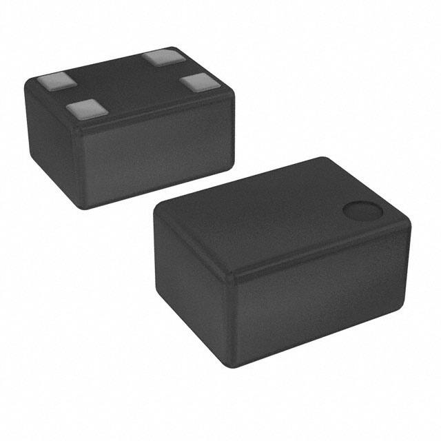
引脚分配: - 引脚1:OE/STBY/FS,具有输出使能、待机模式和频率选择功能。 - 引脚2:GND,电源地。 - 引脚3:OUTPUT,振荡器时钟输出。 - 引脚4:VDD,电源供电。

参数特性: - 供电电压范围:1.71V至3.63V。 - 工作频率范围:2 kHz至100 MHz。 - 功耗:活动模式下3 mA,待机模式下12 µA。 - 频率稳定性:±25 ppm至±50 ppm。 - 工作温度范围:工业级-40°C至85°C,扩展商业级-20°C至70°C。

功能详解: - 该振荡器具有高稳定性、优秀的抗冲击和抗振性能,符合MIL-STD-883标准。 - 可靠性高,MTF(平均故障间隔时间)是石英振荡器的20倍。

应用信息: - 适用于低功耗/便携式应用,如物联网、嵌入式/智能设备。 - 消费类应用,如家庭医疗保健、健身设备、家庭自动化。 - 汽车应用,如倒车/环视摄像头、信息娱乐系统。 - 工业应用,如楼宇/工厂自动化、监控摄像头。

封装信息: - 提供多种封装尺寸,包括1.6 mm x 1.2 mm、2.0 mm x 1.6 mm、2.5 mm x 2.0 mm和3.2 mm x 2.5 mm。 - 这些封装是标准4引脚CMOS石英振荡器的“即插即用”替代品。
DSC6121HI2A-00AHT 价格&库存

很抱歉,暂时无法提供与“DSC6121HI2A-00AHT”相匹配的价格&库存,您可以联系我们找货

免费人工找货