dsPIC30F2011/2012/3012/3013
Data Sheet
High-Performance,
16-bit Digital Signal Controllers
© 2010 Microchip Technology Inc.
DS70139G
�Note the following details of the code protection feature on Microchip devices:
•
Microchip products meet the specification contained in their particular Microchip Data Sheet.
•
Microchip believes that its family of products is one of the most secure families of its kind on the market today, when used in the
intended manner and under normal conditions.
•
There are dishonest and possibly illegal methods used to breach the code protection feature. All of these methods, to our
knowledge, require using the Microchip products in a manner outside the operating specifications contained in Microchip’s Data
Sheets. Most likely, the person doing so is engaged in theft of intellectual property.
•
Microchip is willing to work with the customer who is concerned about the integrity of their code.
•
Neither Microchip nor any other semiconductor manufacturer can guarantee the security of their code. Code protection does not
mean that we are guaranteeing the product as “unbreakable.”
Code protection is constantly evolving. We at Microchip are committed to continuously improving the code protection features of our
products. Attempts to break Microchip’s code protection feature may be a violation of the Digital Millennium Copyright Act. If such acts
allow unauthorized access to your software or other copyrighted work, you may have a right to sue for relief under that Act.
Information contained in this publication regarding device
applications and the like is provided only for your convenience
and may be superseded by updates. It is your responsibility to
ensure that your application meets with your specifications.
MICROCHIP MAKES NO REPRESENTATIONS OR
WARRANTIES OF ANY KIND WHETHER EXPRESS OR
IMPLIED, WRITTEN OR ORAL, STATUTORY OR
OTHERWISE, RELATED TO THE INFORMATION,
INCLUDING BUT NOT LIMITED TO ITS CONDITION,
QUALITY, PERFORMANCE, MERCHANTABILITY OR
FITNESS FOR PURPOSE. Microchip disclaims all liability
arising from this information and its use. Use of Microchip
devices in life support and/or safety applications is entirely at
the buyer’s risk, and the buyer agrees to defend, indemnify and
hold harmless Microchip from any and all damages, claims,
suits, or expenses resulting from such use. No licenses are
conveyed, implicitly or otherwise, under any Microchip
intellectual property rights.
Trademarks
The Microchip name and logo, the Microchip logo, dsPIC,
KEELOQ, KEELOQ logo, MPLAB, PIC, PICmicro, PICSTART,
PIC32 logo, rfPIC and UNI/O are registered trademarks of
Microchip Technology Incorporated in the U.S.A. and other
countries.
FilterLab, Hampshire, HI-TECH C, Linear Active Thermistor,
MXDEV, MXLAB, SEEVAL and The Embedded Control
Solutions Company are registered trademarks of Microchip
Technology Incorporated in the U.S.A.
Analog-for-the-Digital Age, Application Maestro, CodeGuard,
dsPICDEM, dsPICDEM.net, dsPICworks, dsSPEAK, ECAN,
ECONOMONITOR, FanSense, HI-TIDE, In-Circuit Serial
Programming, ICSP, Mindi, MiWi, MPASM, MPLAB Certified
logo, MPLIB, MPLINK, mTouch, Omniscient Code
Generation, PICC, PICC-18, PICDEM, PICDEM.net, PICkit,
PICtail, REAL ICE, rfLAB, Select Mode, Total Endurance,
TSHARC, UniWinDriver, WiperLock and ZENA are
trademarks of Microchip Technology Incorporated in the
U.S.A. and other countries.
SQTP is a service mark of Microchip Technology Incorporated
in the U.S.A.
All other trademarks mentioned herein are property of their
respective companies.
© 2010, Microchip Technology Incorporated, Printed in the
U.S.A., All Rights Reserved.
Printed on recycled paper.
ISBN: 978-1-60932-631-9
Microchip received ISO/TS-16949:2002 certification for its worldwide
headquarters, design and wafer fabrication facilities in Chandler and
Tempe, Arizona; Gresham, Oregon and design centers in California
and India. The Company’s quality system processes and procedures
are for its PIC® MCUs and dsPIC® DSCs, KEELOQ® code hopping
devices, Serial EEPROMs, microperipherals, nonvolatile memory and
analog products. In addition, Microchip’s quality system for the design
and manufacture of development systems is ISO 9001:2000 certified.
DS70139G-page 2
© 2010 Microchip Technology Inc.
�dsPIC30F2011/2012/3012/3013
High-Performance, 16-bit Digital Signal Controllers
Note:
This data sheet summarizes features of
this group of dsPIC30F devices and is not
intended to be a complete reference
source. For more information on the CPU,
peripherals, register descriptions and
general device functionality, refer to the
“dsPIC30F Family Reference Manual”
(DS70046). For more information on the
device instruction set and programming,
refer to the “16-bit MCU and DSC
Programmer’s
Reference
Manual”
(DS70157).
High-Performance Modified RISC CPU:
•
•
•
•
•
•
•
•
•
•
Modified Harvard architecture
C compiler optimized instruction set architecture
Flexible addressing modes
83 base instructions
24-bit wide instructions, 16-bit wide data path
Up to 24 Kbytes on-chip Flash program space
Up to 2 Kbytes of on-chip data RAM
Up to 1 Kbytes of nonvolatile data EEPROM
16 x 16-bit working register array
Up to 30 MIPS operation:
- DC to 40 MHz external clock input
- 4 MHz - 10 MHz oscillator input with
PLL active (4x, 8x, 16x)
• Up to 21 interrupt sources:
- 8 user-selectable priority levels
- 3 external interrupt sources
- 4 processor trap sources
DSP Features:
• Dual data fetch
• Modulo and Bit-Reversed modes
• Two 40-bit wide accumulators with optional
saturation logic
• 17-bit x 17-bit single-cycle hardware fractional/
integer multiplier
• All DSP instructions are single cycle
- Multiply-Accumulate (MAC) operation
• Single-cycle ±16 shift
© 2010 Microchip Technology Inc.
Peripheral Features:
• High-current sink/source I/O pins: 25 mA/25 mA
• Three 16-bit timers/counters; optionally pair up
16-bit timers into 32-bit timer modules
• 16-bit Capture input functions
• 16-bit Compare/PWM output functions
• 3-wire SPI modules (supports four Frame modes)
• I2C™ module supports Multi-Master/Slave mode
and 7-bit/10-bit addressing
• Up to two addressable UART modules with FIFO
buffers
Analog Features:
• 12-bit Analog-to-Digital Converter (ADC) with:
- 200 ksps conversion rate
- Up to 10 input channels
- Conversion available during Sleep and Idle
• Programmable Low-Voltage Detection (PLVD)
• Programmable Brown-out Reset
Special Microcontroller Features:
• Enhanced Flash program memory:
- 10,000 erase/write cycle (min.) for
industrial temperature range, 100K (typical)
• Data EEPROM memory:
- 100,000 erase/write cycle (min.) for
industrial temperature range, 1M (typical)
• Self-reprogrammable under software control
• Power-on Reset (POR), Power-up Timer (PWRT)
and Oscillator Start-up Timer (OST)
• Flexible Watchdog Timer (WDT) with on-chip
low-power RC oscillator for reliable operation
• Fail-Safe Clock Monitor operation:
- Detects clock failure and switches to on-chip
low-power RC oscillator
• Programmable code protection
• In-Circuit Serial Programming™ (ICSP™)
• Selectable Power Management modes:
- Sleep, Idle and Alternate Clock modes
CMOS Technology:
•
•
•
•
Low-power, high-speed Flash technology
Wide operating voltage range (2.5V to 5.5V)
Industrial and Extended temperature ranges
Low-power consumption
DS70139G-page 3
�dsPIC30F2011/2012/3012/3013
dsPIC30F2011/2012/3012/3013 Sensor Family
Input
Cap
Output
Comp/Std
PWM
A/D 12-bit
200 Ksps
I2C™
Timer
16-bit
SPI
EEPROM
Bytes
UART
Program Memory
dsPIC30F2011
18
12K
4K
1024
–
3
2
2
8 ch
1
1
1
dsPIC30F3012
18
24K
8K
2048
1024
3
2
2
8 ch
1
1
1
dsPIC30F2012
28
12K
4K
1024
–
3
2
2
10 ch
1
1
1
dsPIC30F3013
28
24K
8K
2048
1024
3
2
2
10 ch
2
1
1
1
2
3
4
5
6
7
8
9
18
17
16
15
14
13
12
11
10
AVDD
AVSS
AN6/SCK1/INT0/OCFA/RB6
EMUD2/AN7/OC2/IC2/INT2/RB7
VDD
VSS
PGC/EMUC/AN5/U1RX/SDI1/SDA/CN7/RB5
PGD/EMUD/AN4/U1TX/SDO1/SCL/CN6/RB4
EMUC2/OC1/IC1/INT1/RD0
28
27
26
25
24
23
22
21
20
19
18
17
16
15
AVDD
AVSS
AN6/OCFA/RB6
EMUD2/AN7/RB7
AN8/OC1/RB8
AN9/OC2/RB9
CN17/RF4
CN18/RF5
VDD
VSS
PGC/EMUC/U1RX/SDI1/SDA/RF2
PGD/EMUD/U1TX/SDO1/SCL/RF3
SCK1/INT0/RF6
EMUC2/IC1/INT1/RD8
28
27
26
25
24
23
22
21
20
19
18
17
16
15
AVDD
AVSS
AN6/OCFA/RB6
EMUD2/AN7/RB7
AN8/OC1/RB8
AN9/OC2/RB9
U2RX/CN17/RF4
U2TX/CN18/RF5
VDD
VSS
PGC/EMUC/U1RX/SDI1/SDA/RF2
PGD/EMUD/U1TX/SDO1/SCL/RF3
SCK1/INT0/RF6
EMUC2/IC1/INT1/RD8
Device
Bytes
Instructions
SRAM
Bytes
Pins
Pin Diagrams
MCLR
EMUD3/AN0/VREF+/CN2/RB0
EMUC3/AN1/VREF-/CN3/RB1
AN2/SS1/LVDIN/CN4/RB2
AN3/CN5/RB3
OSC1/CLKI
OSC2/CLKO/RC15
EMUD1/SOSCI/T2CK/U1ATX/CN1/RC13
EMUC1/SOSCO/T1CK/U1ARX/CN0/RC14
dsPIC30F3012
dsPIC30F2011
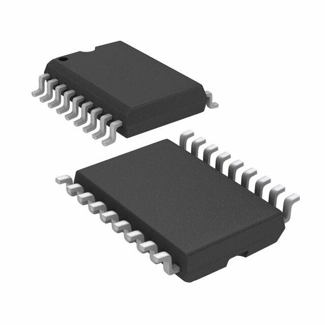
18-Pin PDIP and SOIC
MCLR
EMUD3/AN0/VREF+/CN2/RB0
EMUC3/AN1/VREF-/CN3/RB1
AN2/SS1/LVDIN/CN4/RB2
AN3/CN5/RB3
AN4/CN6/RB4
AN5/CN7/RB5
VSS
OSC1/CLKI
OSC2/CLKO/RC15
EMUD1/SOSCI/T2CK/U1ATX/CN1/RC13
EMUC1/SOSCO/T1CK/U1ARX/CN0/RC14
VDD
IC2/INT2/RD9
1
2
3
4
5
6
7
8
9
10
11
12
13
14
dsPIC30F2012
28-Pin PDIP and SOIC
MCLR
EMUD3/AN0/VREF+/CN2/RB0
EMUC3/AN1/VREF-/CN3/RB1
AN2/SS1/LVDIN/CN4/RB2
AN3/CN5/RB3
AN4/CN6/RB4
AN5/CN7/RB5
VSS
OSC1/CLKI
OSC2/CLKO/RC15
EMUD1/SOSCI/T2CK/U1ATX/CN1/RC13
EMUC1/SOSCO/T1CK/U1ARX/CN0/RC14
VDD
IC2/INT2/RD9
DS70139G-page 4
1
2
3
4
5
6
7
8
9
10
11
12
13
14
dsPIC30F3013
28-Pin SPDIP and SOIC
© 2010 Microchip Technology Inc.
�dsPIC30F2011/2012/3012/3013
Pin Diagrams
28
27
26
25
24
23
22
EMUC3/AN1/VREF-/CN3/RB1
EMUD3/AN0/VREF+/CN2/RB0
MCLR
AVDD
AVSS
AN6/SCK1/INT0/OCFA/RB6
EMUD2/AN7/OC2/IC2/INT2/RB7
28-Pin QFN-S(1)
dsPIC30F2011
8
9
10
11
12
13
14
1
2
3
4
5
6
7
21
20
19
18
17
16
15
NC
NC
NC
NC
VDD
VSS
PGC/EMUC/AN5/U1RX/SDI1/SDA/CN7/RB5
EMUD1/SOSC1/T2CK/U1ATX/CN1/RC13
EMUC1/SOSCO/T1CK/U1ARX/CN0/RC14
VDD
NC
EMUC2/OC1/IC1/INT1/RD0
NC
PGD/EMUD/AN4/U1TX/SDO1/SCL/CN6/RB4
AN2/SS1/LVDIN/CN4/RB2
AN3/CN5/RB3
NC
NC
VSS
OSC1/CLKI
OSC2/CLKO/RC15
Note
1:
The metal plane at the bottom of the device is not connected to any pins and is recommended to be connected to VSS externally.
© 2010 Microchip Technology Inc.
DS70139G-page 5
�dsPIC30F2011/2012/3012/3013
Pin Diagrams
28
27
26
25
24
23
22
EMUC3/AN1/VREF-/CN3/RB1
EMUD3/AN0/VREF+/CN2/RB0
MCLR
AVDD
AVSS
AN6/OCFA/RB6
EMUD2/AN7/RB7
28-Pin QFN-S(1)
dsPIC30F2012
8
9
10
11
12
13
14
1
2
3
4
5
6
7
21
20
19
18
17
16
15
AN8/OC1/RB8
AN9/OC2/RB9
CN17/RF4
CN18/RF5
VDD
VSS
PGC/EMUC/U1RX/SDI1/SDA/RF2
EMUD1/SOSCI/T2CK/U1ATX/CN1/RC13
EMUC1/SOSCO/T1CK/U1ARX/CN0/RC14
VDD
IC2/INT2/RD9
EMUC2/IC1/INT1/RD8
SCK1/INT0/RF6
PGD/EMUD/U1TX/SDO1/SCL/RF3
AN2/SS1/LVDIN/CN4/RB2
AN3/CN5/RB3
AN4/CN6/RB4
AN5/CN7/RB5
VSS
OSC1/CLKI
OSC2/CLKO/RC15
Note
1:
The metal plane at the bottom of the device is not connected to any pins and is recommended to be connected to VSS externally.
DS70139G-page 6
© 2010 Microchip Technology Inc.
�dsPIC30F2011/2012/3012/3013
Pin Diagram
PGD/EMUD/AN4/U1TX/SDO1/SCL/CN6/RB4
NC
EMUC2/OC1/IC1/INT1/RD0
NC
NC
NC
NC
NC
VDD
EMUC1/SOSCO/T1CK/U1ARX/CN0/RC14
EMUD1/SOSCI/T2CK/U1ATX/CN1/RC13
44-Pin QFN(1)
44 43 42 41 40 39 38 37 36 35 34
PGC/EMUC/AN5/U1RX/SDI1/SDA/CN7/RB5
VSS
NC
VDD
NC
NC
NC
NC
NC
NC
NC
1
2
3
4
5
6
7
8
9
10
11
dsPIC30F3012
33
32
31
30
29
28
27
26
25
24
23
OSC2/CLKO/RC15
OSC1/CLKI
VSS
VSS
NC
NC
NC
NC
AN3/CN5/RB3
NC
AN2/SS1/LVDIN/CN4/RB2
EMUD2/AN7/OC2/IC2/INT2/RB7
NC
AN6/SCK1/INT0/OCFA/RB6
NC
AVSS
AVDD
MCLR
EMUD3/AN0/VREF+/CN2/RB0
EMUC3/AN1/VREF-/CN3/RB1
NC
NC
12 13 14 15 16 17 18 19 20 21 22
Note
1:
The metal plane at the bottom of the device is not connected to any pins and is recommended to be connected to VSS externally.
© 2010 Microchip Technology Inc.
DS70139G-page 7
�dsPIC30F2011/2012/3012/3013
Pin Diagrams
44
43
42
41
40
39
38
37
36
35
34
PGD/EMUD/U1TX/SDO1/SCL/RF3
SCK1/INT0/RF6
EMUC2/IC1/INT1/RD8
NC
NC
NC
NC
IC2/INT2/RD9
VDD
EMUC1/SOSCO/T1CK/U1ARX/CN0/RC14
EMUD1/SOSCI/T2CK/U1ATX/CN1/RC13
44-Pin QFN(1)
1
2
3
4
5
6
7
8
9
10
11
dsPIC30F3013
33
32
31
30
29
28
27
26
25
24
23
OSC2/CLKO/RC15
OSC1/CLKI
VSS
VSS
NC
NC
AN5/CN7/RB5
AN4/CN6/RB4
AN3/CN5/RB3
NC
AN2/SS1/LVDIN/CN4/RB2
EMUD2/AN7/RB7
NC
AN6/OCFA/RB6
NC
AVSS
AVDD
MCLR
EMUD3/AN0/VREF+/CN2/RB0
EMUC3/AN1/VREF-/CN3/RB1
NC
NC
12
13
14
15
16
17
18
19
20
21
22
PGC/EMUC/U1RX/SDI1/SDA/RF2
VSS
NC
VDD
NC
NC
U2TX/CN18/RF5
NC
U2RX/CN17/RF4
AN9/OC2/RB9
AN8/OC1/RB8
Note
1:
The metal plane at the bottom of the device is not connected to any pins and is recommended to be connected to VSS externally.
DS70139G-page 8
© 2010 Microchip Technology Inc.
�dsPIC30F2011/2012/3012/3013
Table of Contents
1.0 Device Overview ........................................................................................................................................................................ 11
2.0 CPU Architecture Overview........................................................................................................................................................ 19
3.0 Memory Organization ................................................................................................................................................................. 29
4.0 Address Generator Units............................................................................................................................................................ 43
5.0 Flash Program Memory.............................................................................................................................................................. 49
6.0 Data EEPROM Memory ............................................................................................................................................................. 55
7.0 I/O Ports ..................................................................................................................................................................................... 59
8.0 Interrupts .................................................................................................................................................................................... 65
9.0 Timer1 Module ........................................................................................................................................................................... 73
10.0 Timer2/3 Module ........................................................................................................................................................................ 77
11.0 Input Capture Module................................................................................................................................................................. 83
12.0 Output Compare Module ............................................................................................................................................................ 87
13.0 SPI™ Module ............................................................................................................................................................................. 93
14.0 I2C™ Module ............................................................................................................................................................................. 97
15.0 Universal Asynchronous Receiver Transmitter (UART) Module .............................................................................................. 105
16.0 12-bit Analog-to-Digital Converter (ADC) Module .................................................................................................................... 113
17.0 System Integration ................................................................................................................................................................... 123
18.0 Instruction Set Summary .......................................................................................................................................................... 137
19.0 Development Support............................................................................................................................................................... 145
20.0 Electrical Characteristics .......................................................................................................................................................... 149
21.0 Packaging Information.............................................................................................................................................................. 187
Index .................................................................................................................................................................................................. 201
The Microchip Web Site ..................................................................................................................................................................... 207
Customer Change Notification Service .............................................................................................................................................. 207
Customer Support .............................................................................................................................................................................. 207
Reader Response .............................................................................................................................................................................. 208
Product Identification System ............................................................................................................................................................ 209
TO OUR VALUED CUSTOMERS
It is our intention to provide our valued customers with the best documentation possible to ensure successful use of your Microchip
products. To this end, we will continue to improve our publications to better suit your needs. Our publications will be refined and
enhanced as new volumes and updates are introduced.
If you have any questions or comments regarding this publication, please contact the Marketing Communications Department via
E-mail at docerrors@microchip.com or fax the Reader Response Form in the back of this data sheet to (480) 792-4150. We
welcome your feedback.
Most Current Data Sheet
To obtain the most up-to-date version of this data sheet, please register at our Worldwide Web site at:
http://www.microchip.com
You can determine the version of a data sheet by examining its literature number found on the bottom outside corner of any page.
The last character of the literature number is the version number, (e.g., DS30000A is version A of document DS30000).
Errata
An errata sheet, describing minor operational differences from the data sheet and recommended workarounds, may exist for current
devices. As device/documentation issues become known to us, we will publish an errata sheet. The errata will specify the revision of
silicon and revision of document to which it applies.
To determine if an errata sheet exists for a particular device, please check with one of the following:
• Microchip’s Worldwide Web site; http://www.microchip.com
• Your local Microchip sales office (see last page)
When contacting a sales office, please specify which device, revision of silicon and data sheet (include literature number) you are
using.
Customer Notification System
Register on our web site at www.microchip.com to receive the most current information on all of our products.
© 2010 Microchip Technology Inc.
DS70139G-page 9
�dsPIC30F2011/2012/3012/3013
NOTES:
DS70139G-page 10
© 2010 Microchip Technology Inc.
�dsPIC30F2011/2012/3012/3013
1.0
Note:
DEVICE OVERVIEW
This data sheet summarizes features of
this group of dsPIC30F devices and is not
intended to be a complete reference
source. For more information on the CPU,
peripherals, register descriptions and
general device functionality, refer to the
“dsPIC30F Family Reference Manual”
(DS70046). For more information on the
device instruction set and programming,
refer to the “16-bit MCU and DSC
Programmer’s
Reference
Manual”
(DS70157).
This data sheet contains information specific to the
dsPIC30F2011, dsPIC30F2012, dsPIC30F3012 and
dsPIC30F3013 Digital Signal Controllers (DSC). These
devices contain extensive Digital Signal Processor
(DSP) functionality within a high-performance 16-bit
microcontroller (MCU) architecture.
The following block diagrams depict the architecture for
these devices:
•
•
•
•
Figure 1-1 illustrates the dsPIC30F2011
Figure 1-2 illustrates the dsPIC30F2012
Figure 1-3 illustrates the dsPIC30F3012
Figure 1-4 illustrates the dsPIC30F3013
Following the block diagrams, Table 1-1 relates the I/O
functions to pinout information.
© 2010 Microchip Technology Inc.
DS70139G-page 11
�dsPIC30F2011/2012/3012/3013
FIGURE 1-1:
dsPIC30F2011 BLOCK DIAGRAM
Y Data Bus
X Data Bus
16
16
Interrupt
Controller
PSV & Table
Data Access
24 Control Block
8
Data Latch
Y Data
RAM
(512 bytes)
Address
Latch
16
24
Address Latch
16
16
EMUD3/AN0/VREF+/CN2/RB0
EMUC3/AN1/VREF-/CN3/RB1
AN2/SS1/LVDIN/CN4/RB2
AN3/CN5/RB3
PGD/EMUD/AN4/U1TX/SDO1/SCL/CN6/RB4
PGC/EMUC/AN5/U1RX/SDI1/SDA/CN7/RB5
AN6/SCK1/INT0/OCFA/RB6
EMUD2/AN7/OC2/IC2/INT2/RB7
X RAGU
X WAGU
Y AGU
PCU PCH PCL
Program Counter
Loop
Stack
Control
Control
Logic
Logic
Data Latch
X Data
RAM
(512 bytes)
Address
Latch
16
16
24
Program Memory
(12 Kbytes)
16
16
Data Latch
Effective Address
PORTB
16
ROM Latch
16
24
EMUD1/SOSCI/T2CK/U1ATX/CN1/RC13
EMUC1/SOSCO/T1CK/U1ARX/CN0/RC14
OSC2/CLKO/RC15
IR
16
16
16 x 16
W Reg Array
Decode
PORTC
Instruction
Decode &
Control
16 16
Power-up
Timer
OSC1/CLKI
Timing
Generation
DSP
Engine
VDD, VSS
AVDD, AVSS
Watchdog
Timer
Low-Voltage
Detect
12-bit ADC
DS70139G-page 12
EMUC2/OC1/IC1/INT1/RD0
Oscillator
Start-up Timer
ALU
POR/BOR
Reset
MCLR
Divide
Unit
16
16
PORTD
Input
Capture
Module
Output
Compare
Module
I2C™
Timers
SPI1
UART1
© 2010 Microchip Technology Inc.
�dsPIC30F2011/2012/3012/3013
FIGURE 1-2:
dsPIC30F2012 BLOCK DIAGRAM
Y Data Bus
X Data Bus
16
Interrupt
Controller
PSV & Table
Data Access
24 Control Block
8
16
16
Data Latch
Y Data
RAM
(512 bytes)
Address
Latch
16
24
Address Latch
16
16
EMUD3/AN0/VREF+/CN2/RB0
EMUC3/AN1/VREF-/CN3/RB1
AN2/SS1/LVDIN/CN4/RB2
AN3/CN5/RB3
AN4/CN6/RB4
AN5/CN7/RB5
AN6/OCFA/RB6
EMUD2/AN7/RB7
AN8/OC1/RB8
AN9/OC2/RB9
X RAGU
X WAGU
Y AGU
PCU PCH PCL
Program Counter
Loop
Stack
Control
Control
Logic
Logic
Data Latch
X Data
RAM
(512 bytes)
Address
Latch
16
16
24
Program Memory
(12 Kbytes)
16
Data Latch
Effective Address
16
PORTB
ROM Latch
16
24
IR
16 x 16
W Reg Array
Decode
Instruction
Decode &
Control
Timing
Generation
DSP
Engine
VDD, VSS
AVDD, AVSS
Divide
Unit
EMUC2/IC1/INT1/RD8
IC2/INT2/RD9
Oscillator
Start-up Timer
ALU
POR/BOR
Reset
MCLR
PORTC
16 16
Power-up
Timer
OSC1/CLKI
EMUD1/SOSCI/T2CK/U1ATX/CN1/RC13
EMUC1/SOSCO/T1CK/U1ARX/CN0/RC14
OSC2/CLKO/RC15
16
16
Watchdog
Timer
Low-Voltage
Detect
12-bit ADC
PORTD
16
16
Input
Capture
Module
Output
Compare
Module
I2C™
Timers
SPI1
UART1
PGC/EMUC/U1RX/SDI1/SDA/RF2
PGD/EMUD/U1TX/SDO1/SCL/RF3
CN17/RF4
CN18/RF5
SCK1/INT0/RF6
PORTF
© 2010 Microchip Technology Inc.
DS70139G-page 13
�dsPIC30F2011/2012/3012/3013
FIGURE 1-3:
dsPIC30F3012 BLOCK DIAGRAM
Y Data Bus
X Data Bus
16
16
Interrupt
Controller
PSV & Table
Data Access
24 Control Block 8
Data Latch
Y Data
RAM
(1 Kbytes)
Address
Latch
16
24
Address Latch
Data EEPROM
(1 Kbytes)
16
16
EMUD3/AN0/VREF+/CN2/RB0
EMUC3/AN1/VREF-/CN3/RB1
AN2/SS1/LVDIN/CN4/RB2
AN3/CN5/RB3
PGD/EMUD/AN4/U1TX/SDO1/SCL/CN6/RB4
PGC/EMUC/AN5/U1RX/SDI1/SDA/CN7/RB5
AN6/SCK1/INT0/OCFA/RB6
EMUD2/AN7/OC2/IC2/INT2/RB7
X RAGU
X WAGU
Y AGU
PCU PCH PCL
Program Counter
Loop
Stack
Control
Control
Logic
Logic
Data Latch
X Data
RAM
(1 Kbytes)
Address
Latch
16
16
24
Program Memory
(24 Kbytes)
16
16
Effective Address
PORTB
16
Data Latch
ROM Latch
16
24
EMUD1/SOSCI/T2CK/U1ATX/CN1/RC13
EMUC1/SOSCO/T1CK/U1ARX/CN0/RC14
OSC2/CLKO/RC15
IR
16
16
16 x 16
W Reg Array
Decode
PORTC
Instruction
Decode &
Control
16 16
Power-up
Timer
OSC1/CLKI
Timing
Generation
DSP
Engine
VDD, VSS
AVDD, AVSS
Watchdog
Timer
Low-Voltage
Detect
12-bit ADC
DS70139G-page 14
EMUC2/OC1/IC1/INT1/RD0
Oscillator
Start-up Timer
ALU
POR/BOR
Reset
MCLR
Divide
Unit
16
16
PORTD
Input
Capture
Module
Output
Compare
Module
I2C™
Timers
SPI1
UART1
© 2010 Microchip Technology Inc.
�dsPIC30F2011/2012/3012/3013
FIGURE 1-4:
dsPIC30F3013 BLOCK DIAGRAM
Y Data Bus
X Data Bus
PSV & Table
Data Access
24 Control Block
8
16
16
16
Interrupt
Controller
16
24
Address Latch
16
16
EMUD3/AN0/VREF+/CN2/RB0
EMUC3/AN1/VREF-/CN3/RB1
AN2/SS1/LVDIN/CN4/RB2
AN3/CN5/RB3
AN4/CN6/RB4
AN5/CN7/RB5
AN6/OCFA/RB6
EMUD2/AN7/RB7
AN8/OC1/RB8
AN9/OC2/RB9
X RAGU
X WAGU
Y AGU
PCU PCH PCL
Program Counter
Loop
Stack
Control
Control
Logic
Logic
Data Latch
X Data
RAM
(1 Kbytes)
Address
Latch
16
16
24
Program Memory
(24 Kbytes)
16
Data Latch
Y Data
RAM
(1 Kbytes)
Address
Latch
Data EEPROM
(1 Kbytes)
Data Latch
Effective Address
16
PORTB
ROM Latch
16
24
IR
16
16 x 16
W Reg Array
Decode
Instruction
Decode &
Control
Timing
Generation
DSP
Engine
VDD, VSS
AVDD, AVSS
Divide
Unit
EMUC2/IC1/INT1/RD8
IC2/INT2/RD9
Oscillator
Start-up Timer
ALU
POR/BOR
Reset
MCLR
PORTC
16 16
Power-up
Timer
OSC1/CLKI
EMUD1/SOSCI/T2CK/U1ATX/CN1/RC13
EMUC1/SOSCO/T1CK/U1ARX/CN0/RC14
OSC2/CLKO/RC15
16
Watchdog
Timer
Low-Voltage
Detect
12-bit ADC
PORTD
16
16
Input
Capture
Module
Output
Compare
Module
I2C™
Timers
SPI1
UART1,
UART2
PGC/EMUC/U1RX/SDI1/SDA/RF2
PGD/EMUD/U1TX/SDO1/SCL/RF3
U2RX/CN17/RF4
U2TX/CN18/RF5
SCK1/INT0/RF6
PORTF
© 2010 Microchip Technology Inc.
DS70139G-page 15
�dsPIC30F2011/2012/3012/3013
Table 1-1 provides a brief description of device I/O
pinouts and the functions that may be multiplexed to a
port pin. Multiple functions may exist on one port pin.
When multiplexing occurs, the peripheral module’s
functional requirements may force an override of the
data direction of the port pin.
TABLE 1-1:
PINOUT I/O DESCRIPTIONS
Pin
Type
Buffer
Type
AN0 - AN9
I
Analog
AVDD
P
P
Positive supply for analog module. This pin must be connected at all times.
AVSS
P
P
Ground reference for analog module. This pin must be connected at all times.
CLKI
CLKO
I
O
ST/CMOS
—
External clock source input. Always associated with OSC1 pin function.
Oscillator crystal output. Connects to crystal or resonator in Crystal Oscillator
mode. Optionally functions as CLKO in RC and EC modes. Always associated
with OSC2 pin function.
CN0 - CN7
I
ST
Input change notification inputs.
Can be software programmed for internal weak pull-ups on all inputs.
EMUD
EMUC
EMUD1
EMUC1
EMUD2
EMUC2
EMUD3
EMUC3
I/O
I/O
I/O
I/O
I/O
I/O
I/O
I/O
ST
ST
ST
ST
ST
ST
ST
ST
ICD Primary Communication Channel data input/output pin.
ICD Primary Communication Channel clock input/output pin.
ICD Secondary Communication Channel data input/output pin.
ICD Secondary Communication Channel clock input/output pin.
ICD Tertiary Communication Channel data input/output pin.
ICD Tertiary Communication Channel clock input/output pin.
ICD Quaternary Communication Channel data input/output pin.
ICD Quaternary Communication Channel clock input/output pin.
IC1 - IC2
I
ST
Capture inputs 1 through 2.
INT0
INT1
INT2
I
I
I
ST
ST
ST
External interrupt 0.
External interrupt 1.
External interrupt 2.
LVDIN
I
Analog
MCLR
I/P
ST
Master Clear (Reset) input or programming voltage input. This pin is an
active-low Reset to the device.
OC1-OC2
OCFA
O
I
—
ST
Compare outputs 1 through 2.
Compare Fault A input.
OSC1
I
ST/CMOS
OSC2
I/O
—
PGD
PGC
I/O
I
ST
ST
In-Circuit Serial Programming™ data input/output pin.
In-Circuit Serial Programming clock input pin.
RB0 - RB9
I/O
ST
PORTB is a bidirectional I/O port.
RC13 - RC15
I/O
ST
PORTC is a bidirectional I/O port.
RD0,
RD8-RD9
I/O
ST
PORTD is a bidirectional I/O port.
RF2 - RF5
I/O
ST
PORTF is a bidirectional I/O port.
SCK1
SDI1
SDO1
SS1
I/O
I
O
I
ST
ST
—
ST
Synchronous serial clock input/output for SPI1.
SPI1 Data In.
SPI1 Data Out.
SPI1 Slave Synchronization.
Pin Name
Legend: CMOS =
ST
=
I
=
DS70139G-page 16
Description
Analog input channels.
Low-Voltage Detect Reference Voltage Input pin.
Oscillator crystal input. ST buffer when configured in RC mode; CMOS
otherwise.
Oscillator crystal output. Connects to crystal or resonator in Crystal Oscillator
mode. Optionally functions as CLKO in RC and EC modes.
CMOS compatible input or output
Schmitt Trigger input with CMOS levels
Input
Analog =
O
=
P
=
Analog input
Output
Power
© 2010 Microchip Technology Inc.
�dsPIC30F2011/2012/3012/3013
TABLE 1-1:
PINOUT I/O DESCRIPTIONS (CONTINUED)
Pin
Type
Buffer
Type
SCL
SDA
I/O
I/O
ST
ST
SOSCO
SOSCI
O
I
—
ST/CMOS
T1CK
T2CK
I
I
ST
ST
Timer1 external clock input.
Timer2 external clock input.
U1RX
U1TX
U1ARX
U1ATX
U2RX
U2TX
I
O
I
O
I
O
ST
—
ST
—
ST
—
UART1 Receive.
UART1 Transmit.
UART1 Alternate Receive.
UART1 Alternate Transmit.
UART2 Receive.
UART2 Transmit.
VDD
P
—
Positive supply for logic and I/O pins.
VSS
P
—
Ground reference for logic and I/O pins.
VREF+
I
Analog
Analog Voltage Reference (High) input.
VREF-
I
Analog
Analog Voltage Reference (Low) input.
Pin Name
Legend: CMOS =
ST
=
I
=
Description
Synchronous serial clock input/output for I2C™.
Synchronous serial data input/output for I2C.
32 kHz low-power oscillator crystal output.
32 kHz low-power oscillator crystal input. ST buffer when configured in RC
mode; CMOS otherwise.
CMOS compatible input or output
Schmitt Trigger input with CMOS levels
Input
© 2010 Microchip Technology Inc.
Analog =
O
=
P
=
Analog input
Output
Power
DS70139G-page 17
�dsPIC30F2011/2012/3012/3013
NOTES:
DS70139G-page 18
© 2010 Microchip Technology Inc.
�dsPIC30F2011/2012/3012/3013
2.0
Note:
CPU ARCHITECTURE
OVERVIEW
This data sheet summarizes features of
this group of dsPIC30F devices and is not
intended to be a complete reference
source. For more information on the CPU,
peripherals, register descriptions and
general device functionality, refer to the
“dsPIC30F Family Reference Manual”
(DS70046). For more information on the
device instruction set and programming,
refer to the “16-bit MCU and DSC
Programmer’s
Reference
Manual”
(DS70157).
This section is an overview of the CPU architecture of
the dsPIC30F. The core has a 24-bit instruction word.
The Program Counter (PC) is 23 bits wide with the
Least Significant bit (LSb) always clear (see
Section 3.1 “Program Address Space”). The Most
Significant bit (MSb) is ignored during normal program
execution, except for certain specialized instructions.
Thus, the PC can address up to 4M instruction words
of user program space. An instruction prefetch
mechanism helps maintain throughput. Program loop
constructs, free from loop count management
overhead, are supported using the DO and REPEAT
instructions, both of which are interruptible at any point.
2.1
Core Overview
The working register array consists of 16 x 16-bit
registers, each of which can act as data, address or
offset registers. One working register (W15) operates
as a Software Stack Pointer for interrupts and calls.
The data space is 64 Kbytes (32K words) and is split
into two blocks, referred to as X and Y data memory.
Each block has its own independent Address Generation Unit (AGU). Most instructions operate solely
through the X memory, AGU, which provides the
appearance of a single unified data space. The
Multiply-Accumulate (MAC) class of dual source DSP
instructions operate through both the X and Y AGUs,
splitting the data address space into two parts (see
Section 3.2 “Data Address Space”). The X and Y
data space boundary is device specific and cannot be
altered by the user. Each data word consists of 2 bytes
and most instructions can address data either as words
or bytes.
© 2010 Microchip Technology Inc.
Two ways to access data in program memory are:
• The upper 32 Kbytes of data space memory can
be mapped into the lower half (user space) of
program space at any 16K program word
boundary, defined by the 8-bit Program Space
Visibility Page register (PSVPAG). Thus any
instruction can access program space as if it were
data space, with a limitation that the access
requires an additional cycle. Only the lower 16
bits of each instruction word can be accessed
using this method.
• Linear indirect access of 32K word pages within
program space is also possible using any working
register, via table read and write instructions.
Table read and write instructions can be used to
access all 24 bits of an instruction word.
Overhead-free circular buffers (Modulo Addressing)
are supported in both X and Y address spaces. This is
primarily intended to remove the loop overhead for
DSP algorithms.
The X AGU also supports Bit-Reversed Addressing on
destination effective addresses to greatly simplify input
or output data reordering for radix-2 FFT algorithms.
Refer to Section 4.0 “Address Generator Units” for
details on Modulo and Bit-Reversed Addressing.
The core supports Inherent (no operand), Relative,
Literal, Memory Direct, Register Direct, Register
Indirect, Register Offset and Literal Offset Addressing
modes. Instructions are associated with pre-defined
addressing modes, depending upon their functional
requirements.
For most instructions, the core is capable of executing
a data (or program data) memory read, a working
register (data) read, a data memory write and a
program (instruction) memory read per instruction
cycle. As a result, 3 operand instructions are
supported, allowing C = A+B operations to be executed in a single cycle.
A DSP engine has been included to significantly
enhance the core arithmetic capability and throughput.
It features a high-speed 17-bit by 17-bit multiplier, a
40-bit ALU, two 40-bit saturating accumulators and a
40-bit bidirectional barrel shifter. Data in the
accumulator or any working register can be shifted up
to 15 bits right, or 16 bits left in a single cycle. The DSP
instructions operate seamlessly with all other
instructions and have been designed for optimal
real-time performance. The MAC class of instructions
can concurrently fetch two data operands from memory
while multiplying two W registers. To enable this
concurrent fetching of data operands, the data space
has been split for these instructions and linear is for all
others. This has been achieved in a transparent and
flexible manner, by dedicating certain working registers
to each address space for the MAC
class of
instructions.
DS70139G-page 19
�dsPIC30F2011/2012/3012/3013
The core does not support a multi-stage instruction
pipeline. However, a single-stage instruction prefetch
mechanism is used, which accesses and partially
decodes instructions a cycle ahead of execution, in
order to maximize available execution time. Most
instructions execute in a single cycle with certain
exceptions.
The core features a vectored exception processing
structure for traps and interrupts, with 62 independent
vectors. The exceptions consist of up to 8 traps (of
which 4 are reserved) and 54 interrupts. Each interrupt
is prioritized based on a user-assigned priority between
1 and 7 (1 being the lowest priority and 7 being the
highest), in conjunction with a predetermined ‘natural
order’. Traps have fixed priorities ranging from 8 to 15.
2.2
Programmer’s Model
The programmer’s model is shown in Figure 2-1 and
consists of 16 x 16-bit working registers (W0 through
W15), 2 x 40-bit accumulators (ACCA and ACCB),
STATUS register (SR), Data Table Page register
(TBLPAG), Program Space Visibility Page register
(PSVPAG), DO and REPEAT registers (DOSTART,
DOEND, DCOUNT and RCOUNT) and Program Counter (PC). The working registers can act as data,
address or offset registers. All registers are memory
mapped. W0 acts as the W register for file register
addressing.
Some of these registers have a shadow register associated with each of them, as shown in Figure 2-1. The
shadow register is used as a temporary holding register
and can transfer its contents to or from its host register
upon the occurrence of an event. None of the shadow
registers are accessible directly. The following rules
apply for transfer of registers into and out of shadows.
• PUSH.S and POP.S
W0, W1, W2, W3, SR (DC, N, OV, Z and C bits
only) are transferred.
• DO instruction
DOSTART, DOEND, DCOUNT shadows are
pushed on loop start and popped on loop end.
2.2.1
SOFTWARE STACK POINTER/
FRAME POINTER
The dsPIC® DSC devices contain a software stack.
W15 is the dedicated Software Stack Pointer (SP),
which is automatically modified by exception
processing and subroutine calls and returns. However,
W15 can be referenced by any instruction in the same
manner as all other W registers. This simplifies the
reading, writing and manipulation of the Stack Pointer
(e.g., creating stack frames).
Note:
In order to protect against misaligned
stack accesses, W15 is always clear.
W15 is initialized to 0x0800 during a Reset. The user
may reprogram the SP during initialization to any
location within data space.
W14 has been dedicated as a Stack Frame Pointer, as
defined by the LNK and ULNK instructions. However,
W14 can be referenced by any instruction in the same
manner as all other W registers.
2.2.2
STATUS REGISTER
The dsPIC DSC core has a 16-bit STATUS register
(SR), the LSB of which is referred to as the SR Low
byte (SRL) and the MSB as the SR High byte (SRH).
See Figure 2-1 for SR layout.
SRL contains all the MCU ALU operation Status flags
(including the Z bit), as well as the CPU Interrupt
Priority Level Status bits, IPL, and the Repeat
Active Status bit, RA. During exception processing,
SRL is concatenated with the MSB of the PC to form a
complete word value which is then stacked.
The upper byte of the STATUS register contains the
DSP Adder/Subtracter Status bits, the DO Loop Active
bit (DA) and the Digit Carry (DC) Status bit.
2.2.3
PROGRAM COUNTER
The program counter is 23 bits wide; bit 0 is always
clear. Therefore, the PC can address up to 4M
instruction words.
When a byte operation is performed on a working register, only the Least Significant Byte (LSB) of the target
register is affected. However, a benefit of memory
mapped working registers is that both the Least and
Most Significant Bytes (MSB) can be manipulated
through byte-wide data memory space accesses.
DS70139G-page 20
© 2010 Microchip Technology Inc.
�dsPIC30F2011/2012/3012/3013
FIGURE 2-1:
PROGRAMMER’S MODEL
D15
D0
W0/WREG
PUSH.S Shadow
W1
DO Shadow
W2
W3
Legend
W4
DSP Operand
Registers
W5
W6
W7
Working Registers
W8
W9
DSP Address
Registers
W10
W11
W12/DSP Offset
W13/DSP Write-Back
W14/Frame Pointer
W15/Stack Pointer
Stack Pointer Limit Register
SPLIM
AD39
AD15
AD31
AD0
ACCA
DSP
Accumulators
ACCB
PC22
PC0
Program Counter
0
0
7
TABPAG
TBLPAG
7
Data Table Page Address
0
PSVPAG
Program Space Visibility Page Address
15
0
RCOUNT
REPEAT Loop Counter
15
0
DCOUNT
DO Loop Counter
22
0
DOSTART
DO Loop Start Address
DOEND
DO Loop End Address
22
15
0
Core Configuration Register
CORCON
OA
OB
SA
SB OAB SAB DA
SRH
© 2010 Microchip Technology Inc.
DC IPL2 IPL1 IPL0 RA
N
OV
Z
C
STATUS register
SRL
DS70139G-page 21
�dsPIC30F2011/2012/3012/3013
2.3
Divide Support
The dsPIC DSC devices feature a 16/16-bit signed
fractional divide operation, as well as 32/16-bit and
16/16-bit signed and unsigned integer divide operations, in the form of single instruction iterative divides.
The following instructions and data sizes are
supported:
1.
2.
3.
4.
5.
DIVF - 16/16 signed fractional divide
DIV.sd - 32/16 signed divide
DIV.ud - 32/16 unsigned divide
DIV.s - 16/16 signed divide
DIV.u - 16/16 unsigned divide
The divide instructions must be executed within a
REPEAT loop. Any other form of execution
(e.g., a series of discrete divide instructions) will not
function correctly because the instruction flow depends
on RCOUNT. The divide instruction does not
automatically set up the RCOUNT value and it must,
therefore, be explicitly and correctly specified in the
REPEAT instruction, as shown in Table 2-1 (REPEAT
executes the target instruction {operand value+1}
times). The REPEAT loop count must be setup for 18
iterations of the DIV/DIVF instruction. Thus, a
complete divide operation requires 19 cycles.
Note:
The 16/16 divides are similar to the 32/16 (same number
of iterations), but the dividend is either zero-extended or
sign-extended during the first iteration.
TABLE 2-1:
DIVIDE INSTRUCTIONS
Instruction
DIVF
Function
Signed fractional divide: Wm/Wn →W0; Rem →W1
DIV.sd
Signed divide: (Wm+1:Wm)/Wn →W0; Rem →W1
DIV.s
Signed divide: Wm/Wn →W0; Rem →W1
DIV.ud
Unsigned divide: (Wm+1:Wm)/Wn →W0; Rem →W1
DIV.u
Unsigned divide: Wm/Wn →W0; Rem →W1
DS70139G-page 22
The divide flow is interruptible; however,
the user needs to save the context as
appropriate.
© 2010 Microchip Technology Inc.
�dsPIC30F2011/2012/3012/3013
2.4
DSP Engine
The DSP engine consists of a high-speed 17-bit x
17-bit multiplier, a barrel shifter and a 40-bit
adder/subtracter (with two target accumulators, round
and saturation logic).
The DSP engine also has the capability to perform
inherent
accumulator-to-accumulator
operations,
which require no additional data. These instructions are
ADD, SUB and NEG.
The dsPIC30F is a single-cycle instruction flow
architecture, therefore, concurrent operation of the
DSP engine with MCU instruction flow is not possible.
However, some MCU ALU and DSP engine resources
may be used concurrently by the same instruction
(e.g., ED, EDAC). See Table 2-2.
TABLE 2-2:
ACC WB?
CLR
A=0
Yes
ED
A = (x – y)2
7.
Fractional or integer DSP multiply (IF).
Signed or unsigned DSP multiply (US).
Conventional or convergent rounding (RND).
Automatic saturation on/off for ACCA (SATA).
Automatic saturation on/off for ACCB (SATB).
Automatic saturation on/off for writes to data
memory (SATDW).
Accumulator Saturation mode selection
(ACCSAT).
Note:
For CORCON layout, see Table 3-3.
A block diagram of the DSP engine is shown in
Figure 2-2.
No
y)2
No
MAC
A = A + (x * y)
Yes
MAC
A = A + x2
No
MOVSAC
No change in A
Yes
EDAC
1.
2.
3.
4.
5.
6.
DSP INSTRUCTION
SUMMARY
Algebraic
Operation
Instruction
The DSP engine has several options selected through
various bits in the CPU Core Configuration register
(CORCON), which are:
A = A + (x –
MPY
A=x•y
No
MPY.N
A=–x•y
No
MSC
A=A–x• y
Yes
© 2010 Microchip Technology Inc.
DS70139G-page 23
�dsPIC30F2011/2012/3012/3013
FIGURE 2-2:
DSP ENGINE BLOCK DIAGRAM
40
40-bit Accumulator A
40-bit Accumulator B
Carry/Borrow Out
Carry/Borrow In
40
Saturate
S
a
Round t 16
u
Logic r
a
t
e
Adder
Negate
40
40
40
Barrel
Shifter
16
X Data Bus
40
Y Data Bus
Sign-Extend
32
16
Zero Backfill
32
33
17-bit
Multiplier/Scaler
16
16
To/From W Array
DS70139G-page 24
© 2010 Microchip Technology Inc.
�dsPIC30F2011/2012/3012/3013
2.4.1
MULTIPLIER
The 17 x 17-bit multiplier is capable of signed or
unsigned operation and can multiplex its output using a
scaler to support either 1.31 fractional (Q31) or 32-bit
integer results. Unsigned operands are zero-extended
into the 17th bit of the multiplier input value. Signed
operands are sign-extended into the 17th bit of the
multiplier input value. The output of the 17 x 17-bit
multiplier/scaler is a 33-bit value which is
sign-extended to 40 bits. Integer data is inherently
represented as a signed two’s complement value,
where the MSB is defined as a sign bit. Generally
speaking, the range of an N-bit two’s complement
integer is -2N-1 to 2N-1 – 1. For a 16-bit integer, the data
range is -32768 (0x8000) to 32767 (0x7FFF) including
‘0’. For a 32-bit integer, the data range is
-2,147,483,648 (0x8000 0000) to 2,147,483,645
(0x7FFF FFFF).
When the multiplier is configured for fractional
multiplication, the data is represented as a two’s
complement fraction, where the MSB is defined as a
sign bit and the radix point is implied to lie just after the
sign bit (QX format). The range of an N-bit two’s
complement fraction with this implied radix point is -1.0
to (1 – 21-N). For a 16-bit fraction, the Q15 data range
is -1.0 (0x8000) to 0.999969482 (0x7FFF) including ‘0’
and has a precision of 3.01518x10⁻⁵. In Fractional
mode, the 16x16 multiply operation generates a 1.31
product, which has a precision of 4.65661 x 10⁻¹⁰.
The same multiplier is used to support the MCU
multiply instructions, which include integer 16-bit
signed, unsigned and mixed sign multiplies.
The MUL instruction can be directed to use byte or
word-sized operands. Byte operands direct a 16-bit
result. Word operands direct a 32-bit result to the
specified register(s) in the W array.
2.4.2
DATA ACCUMULATORS AND
ADDER/SUBTRACTER
The data accumulator consists of a 40-bit
adder/subtracter with automatic sign extension logic. It
can select one of two accumulators (A or B) as its
pre-accumulation source and post-accumulation
destination. For the ADD and LAC instructions, the data
to be accumulated or loaded can be optionally scaled
through the barrel shifter prior to accumulation.
© 2010 Microchip Technology Inc.
2.4.2.1
Adder/Subtracter, Overflow and
Saturation
The adder/subtracter is a 40-bit adder with an optional
zero input into one side and either true or complement
data into the other input. In the case of addition, the
carry/borrow input is active high and the other input is
true data (not complemented), whereas in the case of
subtraction, the carry/borrow input is active low and the
other input is complemented. The adder/subtracter
generates overflow status bits SA/SB and OA/OB,
which are latched and reflected in the STATUS register:
• Overflow from bit 39: This is a catastrophic
overflow in which the sign of the accumulator is
destroyed.
• Overflow into guard bits 32 through 39: This is a
recoverable overflow. This bit is set whenever all
the guard bits are not identical to each other.
The adder has an additional saturation block which
controls accumulator data saturation if selected. It uses
the result of the adder, the overflow Status bits
described above, and the mode control bits SATA/B
(CORCON) and ACCSAT (CORCON) to
determine when and to what value to saturate.
Six STATUS register bits have been provided to
support saturation and overflow. They are:
• OA: ACCA overflowed into guard bits
• OB: ACCB overflowed into guard bits
• SA: ACCA saturated (bit 31 overflow and
saturation)
or
ACCA overflowed into guard bits and saturated
(bit 39 overflow and saturation)
• SB: ACCB saturated (bit 31 overflow and
saturation)
or
ACCB overflowed into guard bits and saturated
(bit 39 overflow and saturation)
• OAB: Logical OR of OA and OB
• SAB: Logical OR of SA and SB
The OA and OB bits are modified each time data
passes through the adder/subtracter. When set, they
indicate that the most recent operation has overflowed
into the accumulator guard bits (bits 32 through 39).
The OA and OB bits can also optionally generate an
arithmetic warning trap when set and the
corresponding overflow trap flag enable bit (OVATE,
OVBTE) in the INTCON1 register (refer to Section 8.0
“Interrupts”) is set. This allows the user to take
immediate action, for example, to correct system gain.
DS70139G-page 25
�dsPIC30F2011/2012/3012/3013
The SA and SB bits are modified each time data
passes through the adder/subtracter but can only be
cleared by the user. When set, they indicate that the
accumulator has overflowed its maximum range (bit 31
for 32-bit saturation or bit 39 for 40-bit saturation) and
will be saturated if saturation is enabled. When saturation is not enabled, SA and SB default to bit 39 overflow
and thus indicate that a catastrophic overflow has
occurred. If the COVTE bit in the INTCON1 register is
set, SA and SB bits generate an arithmetic warning trap
when saturation is disabled.
The overflow and saturation Status bits can optionally
be viewed in the STATUS register (SR) as the logical
OR of OA and OB (in bit OAB) and the logical OR of SA
and SB (in bit SAB). This allows programmers to check
one bit in the STATUS register to determine if either
accumulator has overflowed, or one bit to determine if
either accumulator has saturated. This would be useful
for complex number arithmetic which typically uses
both the accumulators.
The device supports three saturation and overflow
modes:
1.
2.
3.
Bit 39 Overflow and Saturation:
When bit 39 overflow and saturation occurs, the
saturation logic loads the maximally positive 9.31
(0x7FFFFFFFFF) or maximally negative 9.31
value
(0x8000000000)
into the target
accumulator. The SA or SB bit is set and remains
set until cleared by the user. This is referred to as
‘super saturation’ and provides protection against
erroneous data or unexpected algorithm
problems (e.g., gain calculations).
Bit 31 Overflow and Saturation:
When bit 31 overflow and saturation occurs, the
saturation logic then loads the maximally positive 1.31 value (0x007FFFFFFF) or maximally
negative 1.31 value (0x0080000000) into the
target accumulator. The SA or SB bit is set and
remains set until cleared by the user. When this
Saturation mode is in effect, the guard bits are
not used, so the OA, OB or OAB bits are never
set.
Bit 39 Catastrophic Overflow:
The bit 39 overflow Status bit from the adder is
used to set the SA or SB bit which remains set
until cleared by the user. No saturation operation
is performed and the accumulator is allowed to
overflow (destroying its sign). If the COVTE bit in
the INTCON1 register is set, a catastrophic
overflow can initiate a trap exception.
DS70139G-page 26
2.4.2.2
Accumulator ‘Write-Back’
The MAC class of instructions (with the exception of
MPY, MPY.N, ED and EDAC) can optionally write a
rounded version of the high word (bits 31 through 16)
of the accumulator that is not targeted by the instruction
into data space memory. The write is performed across
the X bus into combined X and Y address space. The
following addressing modes are supported:
1.
2.
W13, Register Direct:
The rounded contents of the non-target
accumulator are written into W13 as a 1.15
fraction.
[W13]+
=
2,
Register
Indirect
with
Post-Increment:
The rounded contents of the non-target
accumulator are written into the address pointed
to by W13 as a 1.15 fraction. W13 is then
incremented by 2 (for a word write).
2.4.2.3
Round Logic
The round logic is a combinational block which
performs a conventional (biased) or convergent
(unbiased) round function during an accumulator write
(store). The Round mode is determined by the state of
the RND bit in the CORCON register. It generates a
16-bit, 1.15 data value, which is passed to the data
space write saturation logic. If rounding is not indicated
by the instruction, a truncated 1.15 data value is stored
and the least significant word (lsw) is simply discarded.
Conventional rounding takes bit 15 of the accumulator,
zero-extends it and adds it to the ACCxH word (bits 16
through 31 of the accumulator). If the ACCxL word
(bits 0 through 15 of the accumulator) is between
0x8000 and 0xFFFF (0x8000 included), ACCxH is
incremented. If ACCxL is between 0x0000 and 0x7FFF,
ACCxH is left unchanged. A consequence of this
algorithm is that over a succession of random rounding
operations, the value tends to be biased slightly
positive.
Convergent (or unbiased) rounding operates in the
same manner as conventional rounding, except when
ACCxL equals 0x8000. If this is the case, the LSb
(bit 16 of the accumulator) of ACCxH is examined. If it
is ‘1’, ACCxH is incremented. If it is ‘0’, ACCxH is not
modified. Assuming that bit 16 is effectively random in
nature, this scheme will remove any rounding bias that
may accumulate.
The SAC and SAC.R instructions store either a
truncated (SAC) or rounded (SAC.R) version of the
contents of the target accumulator to data memory via
the X bus (subject to data saturation, see
Section 2.4.2.4 “Data Space Write Saturation”).
Note that for the MAC class of instructions, the
accumulator write-back operation functions in the
same manner, addressing combined MCU (X and Y)
data space though the X bus. For this class of
instructions, the data is always subject to rounding.
© 2010 Microchip Technology Inc.
�dsPIC30F2011/2012/3012/3013
2.4.2.4
Data Space Write Saturation
2.4.3
BARREL SHIFTER
In addition to adder/subtracter saturation, writes to data
space may also be saturated but without affecting the
contents of the source accumulator. The data space
write saturation logic block accepts a 16-bit, 1.15
fractional value from the round logic block as its input,
together with overflow status from the original source
(accumulator) and the 16-bit round adder. These are
combined and used to select the appropriate 1.15
fractional value as output to write to data space
memory.
The barrel shifter is capable of performing up to 16-bit
arithmetic or logic right shifts, or up to 16-bit left shifts
in a single cycle. The source can be either of the two
DSP accumulators, or the X bus (to support multi-bit
shifts of register or memory data).
If the SATDW bit in the CORCON register is set, data
(after rounding or truncation) is tested for overflow and
adjusted accordingly. For input data greater than
0x007FFF, data written to memory is forced to the
maximum positive 1.15 value, 0x7FFF. For input data
less than 0xFF8000, data written to memory is forced
to the maximum negative 1.15 value, 0x8000. The MSb
of the source (bit 39) is used to determine the sign of
the operand being tested.
The barrel shifter is 40 bits wide, thereby obtaining a
40-bit result for DSP shift operations and a 16-bit result
for MCU shift operations. Data from the X bus is
presented to the barrel shifter between bit positions 16
to 31 for right shifts, and bit positions 0 to 16 for left
shifts.
The shifter requires a signed binary value to determine
both the magnitude (number of bits) and direction of the
shift operation. A positive value shifts the operand right.
A negative value shifts the operand left. A value of ‘0’
does not modify the operand.
If the SATDW bit in the CORCON register is not set, the
input data is always passed through unmodified under
all conditions.
© 2010 Microchip Technology Inc.
DS70139G-page 27
�dsPIC30F2011/2012/3012/3013
NOTES:
DS70139G-page 28
© 2010 Microchip Technology Inc.
�dsPIC30F2011/2012/3012/3013
3.0
Note:
3.1
MEMORY ORGANIZATION
This data sheet summarizes features of
this group of dsPIC30F devices and is not
intended to be a complete reference
source. For more information on the CPU,
peripherals, register descriptions and
general device functionality, refer to the
“dsPIC30F Family Reference Manual”
(DS70046). For more information on the
device instruction set and programming,
refer to the “16-bit MCU and DSC
Programmer’s
Reference
Manual”
(DS70157).
Program Address Space
The program address space is 4M instruction words.
The program space memory maps for the
dsPIC30F2011/2012/3012/3013 devices is shown in
Figure 3-1.
Program memory is addressable by a 24-bit value from
either the 23-bit PC, table instruction Effective Address
(EA), or data space EA, when program space is
mapped into data space as defined by Table 3-1. Note
that the program space address is incremented by two
between successive program words in order to provide
compatibility with data space addressing.
User program space access is restricted to the lower
4M instruction word address range (0x000000 to
0x7FFFFE) for all accesses other than TBLRD/TBLWT,
which uses TBLPAG to determine user or configuration space access. In Table 3-1, Program Space
Address Construction, bit 23 allows access to the
Device ID, the User ID and the Configuration bits.
Otherwise, bit 23 is always clear.
© 2010 Microchip Technology Inc.
DS70139G-page 29
�dsPIC30F2011/2012/3012/3013
FIGURE 3-1:
PROGRAM SPACE MEMORY MAPS
dsPIC30F2011/2012
Reset - GOTO Instruction
Reset - Target Address
dsPIC30F3012/3013
Reset - GOTO Instruction
Reset - Target Address
000000
000002
000004
Interrupt Vector Table
Interrupt Vector Table
Vector Tables
Reserved
Vector Tables
00007E
000080
000084
Reserved
0000FE
000100
001FFE
002000
User Flash
Program Memory
(8K instructions)
Reserved
(Read ‘0’s)
Reserved
(Read ‘0’s)
Data EEPROM
(1 Kbyte)
7FFFFE
800000
F7FFFE
F80000
F8000E
F80010
Reserved
DS70139G-page 30
Configuration Memory
Space
Configuration Memory
Space
8005BE
8005C0
Reserved
DEVID (2)
003FFE
004000
7FFBFE
7FFC00
Reserved
8005FE
800600
Device Configuration
Registers
000084
0000FE
000100
7FFFFE
800000
Reserved
UNITID (32 instr.)
00007E
000080
Alternate Vector Table
User Memory
Space
User Memory
Space
Alternate Vector Table
User Flash
Program Memory
(4K instructions)
000000
000002
000004
UNITID (32 instr.)
8005BE
8005C0
8005FE
800600
Reserved
Device Configuration
Registers
F7FFFE
F80000
F8000E
F80010
Reserved
FEFFFE
FF0000
FFFFFE
DEVID (2)
FEFFFE
FF0000
FFFFFE
© 2010 Microchip Technology Inc.
�dsPIC30F2011/2012/3012/3013
TABLE 3-1:
PROGRAM SPACE ADDRESS CONSTRUCTION
Program Space Address
Access
Space
Access Type
Instruction Access
User
TBLRD/TBLWT
User
(TBLPAG = 0)
TBLPAG
Data EA
TBLRD/TBLWT
Configuration
(TBLPAG = 1)
TBLPAG
Data EA
Program Space Visibility
User
FIGURE 3-2:
PC
0
0
PSVPAG
0
Data EA
DATA ACCESS FROM PROGRAM SPACE ADDRESS GENERATION
23 bits
Using
Program
Counter
Program Counter
0
Select
Using
Program
Space
Visibility
0
1
0
EA
PSVPAG Reg
8 bits
15 bits
EA
Using
Table
Instruction
1/0
User/
Configuration
Space
Select
Note:
TBLPAG Reg
8 bits
16 bits
24-bit EA
Byte
Select
Program space visibility cannot be used to access bits of a word in program memory.
© 2010 Microchip Technology Inc.
DS70139G-page 31
�dsPIC30F2011/2012/3012/3013
3.1.1
DATA ACCESS FROM PROGRAM
MEMORY USING TABLE
INSTRUCTIONS
A set of table instructions are provided to move byte or
word-sized data to and from program space. See
Figure 3-4 and Figure 3-5.
1.
This architecture fetches 24-bit wide program memory.
Consequently, instructions are always aligned.
However, as the architecture is modified Harvard, data
can also be present in program space.
There are two methods by which program space can
be accessed: via special table instructions, or through
the remapping of a 16K word program space page into
the upper half of data space (see Section 3.1.2 “Data
Access from Program Memory Using Program
Space Visibility”). The TBLRDL and TBLWTL
instructions offer a direct method of reading or writing
the lsw of any address within program space, without
going through data space. The TBLRDH and TBLWTH
instructions are the only method whereby the upper 8
bits of a program space word can be accessed as data.
2.
3.
The PC is incremented by two for each successive
24-bit program word. This allows program memory
addresses to directly map to data space addresses.
Program memory can thus be regarded as two 16-bit
word wide address spaces, residing side by side, each
with the same address range. TBLRDL and TBLWTL
access the space which contains the lsw, and TBLRDH
and TBLWTH access the space which contains the
MSB.
4.
TBLRDL: Table Read Low
Word: Read the LS Word of the program address;
P maps to D.
Byte: Read one of the LSB of the program
address;
P maps to the destination byte when byte
select = 0;
P maps to the destination byte when byte
select = 1.
TBLWTL: Table Write Low (refer to Section 5.0
“Flash Program Memory” for details on Flash
Programming)
TBLRDH: Table Read High
Word: Read the MS Word of the program address;
P maps to D; D will always
be = 0.
Byte: Read one of the MSB of the program
address;
P maps to the destination byte when
byte select = 0;
The destination byte will always be = 0 when
byte select = 1.
TBLWTH: Table Write High (refer to Section 5.0
“Flash Program Memory” for details on Flash
Programming)
Figure 3-2 shows how the EA is created for table
operations and data space accesses (PSV = 1). Here,
P refers to a program space word, whereas
D refers to a data space word.
FIGURE 3-3:
PROGRAM DATA TABLE ACCESS (lsw)
PC Address
0x000000
0x000002
0x000004
0x000006
Program Memory
‘Phantom’ Byte
(read as ‘0’)
DS70139G-page 32
23
16
8
0
00000000
00000000
00000000
00000000
TBLRDL.W
TBLRDL.B (Wn = 0)
TBLRDL.B (Wn = 1)
© 2010 Microchip Technology Inc.
�dsPIC30F2011/2012/3012/3013
FIGURE 3-4:
PROGRAM DATA TABLE ACCESS (MSB)
TBLRDH.W
PC Address
0x000000
0x000002
0x000004
0x000006
23
16
8
0
00000000
00000000
00000000
00000000
TBLRDH.B (Wn = 0)
Program Memory
‘Phantom’ Byte
(read as ‘0’)
3.1.2
TBLRDH.B (Wn = 1)
DATA ACCESS FROM PROGRAM
MEMORY USING PROGRAM SPACE
VISIBILITY
The upper 32 Kbytes of data space may optionally be
mapped into any 16K word program space page. This
provides transparent access of stored constant data
from X data space without the need to use special
instructions (i.e., TBLRDL/H, TBLWTL/H instructions).
Program space access through the data space occurs
if the MSb of the data space EA is set and program
space visibility is enabled by setting the PSV bit in the
Core Control register (CORCON). The functions of
CORCON are discussed in Section 2.4 “DSP
Engine”.
Data accesses to this area add an additional cycle to
the instruction being executed, since two program
memory fetches are required.
Note that the upper half of addressable data space is
always part of the X data space. Therefore, when a
DSP operation uses program space mapping to access
this memory region, Y data space should typically
contain state (variable) data for DSP operations,
whereas X data space should typically contain
coefficient (constant) data.
Although each data space address, 0x8000 and higher,
maps directly into a corresponding program memory
address (see Figure 3-5), only the lower 16 bits of the
24-bit program word are used to contain the data. The
upper 8 bits should be programmed to force an illegal
instruction to maintain machine robustness. Refer to
the “16-bit MCU and DSC Programmer’s Reference
Manual” (DS70157) for details on instruction encoding.
© 2010 Microchip Technology Inc.
Note that by incrementing the PC by 2 for each
program memory word, the LS 15 bits of data space
addresses directly map to the LS 15 bits in the
corresponding program space addresses. The
remaining bits are provided by the Program Space
Visibility Page register, PSVPAG, as shown in
Figure 3-5.
Note:
PSV access is temporarily disabled during
table reads/writes.
For instructions that use PSV which are executed
outside a REPEAT loop:
• The following instructions require one instruction
cycle in addition to the specified execution time:
- MAC class of instructions with data operand
prefetch
- MOV instructions
- MOV.D instructions
• All other instructions require two instruction cycles
in addition to the specified execution time of the
instruction.
For instructions that use PSV which are executed
inside a REPEAT loop:
• The following instances require two instruction
cycles in addition to the specified execution time
of the instruction:
- Execution in the first iteration
- Execution in the last iteration
- Execution prior to exiting the loop due to an
interrupt
- Execution upon re-entering the loop after an
interrupt is serviced
• Any other iteration of the REPEAT loop allow the
instruction accessing data, using PSV, to execute
in a single cycle.
DS70139G-page 33
�dsPIC30F2011/2012/3012/3013
FIGURE 3-5:
DATA SPACE WINDOW INTO PROGRAM SPACE OPERATION
Data Space
Program Space
0x0000
PSVPAG(1)
0x00
8
15
EA = 0
Data 16
Space
15
EA
EA = 1
0x000000
0x8000
15
Address
Concatenation 23
23
15
0
0x001200
Upper Half of Data
Space is Mapped
into Program Space
0x001FFF
0xFFFF
Data Read
BSET
MOV
MOV
MOV
CORCON,#2 ; Set PSV bit
#0x0, W0
; Set PSVPAG register
W0, PSVPAG
0x9200, W0 ; Access program memory location
; using a data space access
Note 1: PSVPAG is an 8-bit register, containing bits of the program space address.
DS70139G-page 34
© 2010 Microchip Technology Inc.
�dsPIC30F2011/2012/3012/3013
3.2
Data Address Space
The core has two data spaces. The data spaces can be
considered either separate (for some DSP
instructions), or as one unified linear address range (for
MCU instructions). The data spaces are accessed
using two Address Generation Units (AGUs) and
separate data paths.
3.2.1
DATA SPACE MEMORY MAP
The data space memory is split into two blocks, X and
Y data space. A key element of this architecture is that
Y space is a subset of X space, and is fully contained
within X space. In order to provide an apparent Linear
Addressing space, X and Y spaces have contiguous
addresses.
FIGURE 3-6:
When executing any instruction other than one of the
MAC class of instructions, the X block consists of the 64
Kbyte data address space (including all Y addresses).
When executing one of the MAC class of instructions,
the X block consists of the 64 Kbyte data address
space, excluding the Y address block (for data reads
only). In other words, all other instructions regard the
entire data memory as one composite address space.
The MAC class instructions extract the Y address space
from data space and address it using EAs sourced from
W10 and W11. The remaining X data space is
addressed using W8 and W9. Both address spaces are
concurrently accessed only with the MAC class
instructions.
The data space memory map for the dsPIC30F2011
and dsPIC30F2012 is shown in Figure 3-6. The data
space memory map for the dsPIC30F3012 and
dsPIC30F3013 is shown in Figure 3-7.
dsPIC30F2011/2012 DATA SPACE MEMORY MAP
MSB
Address
MSB
2 Kbyte
SFR Space
1 Kbyte
SRAM Space
LSB
0x0000
0x0001
SFR Space
0x07FF
0x0801
0x09FF
0x0A01
0x07FE
0x0800
X Data RAM (X)
0x09FE
0x0A00
Y Data RAM (Y)
0x0BFF
0x0C01
0x0BFE
0x0C00
0x1FFF
0x1FFE
0x8001
0x8000
8 Kbyte
Near
Data
Space
X Data
Unimplemented (X)
Optionally
Mapped
into Program
Memory
0xFFFF
© 2010 Microchip Technology Inc.
LSB
Address
16 bits
0xFFFE
DS70139G-page 35
�dsPIC30F2011/2012/3012/3013
FIGURE 3-7:
dsPIC30F3012/3013 DATA SPACE MEMORY MAP
MSB
Address
16 bits
MSB
2 Kbyte
SFR Space
2 Kbyte
SRAM Space
LSB
0x0000
0x0001
SFR Space
0x07FE
0x0800
0x07FF
0x0801
0x0BFF
0x0C01
X Data RAM (X)
8 Kbyte
Near
Data
Space
0x0BFE
0x0C00
Y Data RAM (Y)
0x0FFF
0x1001
0x0FFE
0x1000
0x1FFF
0x1FFE
0x8001
0x8000
X Data
Unimplemented (X)
Optionally
Mapped
into Program
Memory
0xFFFF
DS70139G-page 36
LSB
Address
0xFFFE
© 2010 Microchip Technology Inc.
�dsPIC30F2011/2012/3012/3013
DATA SPACE FOR MCU AND DSP (MAC CLASS) INSTRUCTIONS EXAMPLE
SFR SPACE
SFR SPACE
X SPACE
FIGURE 3-8:
Y SPACE
UNUSED
X SPACE
(Y SPACE)
X SPACE
UNUSED
UNUSED
Non-MAC Class Ops (Read/Write)
MAC Class Ops (Write)
Indirect EA using any W
© 2010 Microchip Technology Inc.
MAC Class Ops (Read)
Indirect EA using W8, W9
Indirect EA using W10, W11
DS70139G-page 37
�dsPIC30F2011/2012/3012/3013
3.2.2
DATA SPACES
3.2.3
The X data space is used by all instructions and supports all addressing modes. There are separate read
and write data buses. The X read data bus is the return
data path for all instructions that view data space as
combined X and Y address space. It is also the X
address space data path for the dual operand read
instructions (MAC class). The X write data bus is the
only write path to data space for all instructions.
The X data space also supports Modulo Addressing for
all instructions, subject to Addressing mode restrictions. Bit-Reversed Addressing is only supported for
writes to X data space.
The Y data space is used in concert with the X data
space by the MAC class of instructions (CLR, ED,
EDAC, MAC, MOVSAC, MPY, MPY.N and MSC) to
provide two concurrent data read paths. No writes
occur across the Y bus. This class of instructions
dedicates two W register pointers, W10 and W11, to
always address Y data space, independent of X data
space, whereas W8 and W9 always address X data
space. Note that during accumulator write back, the
data address space is considered a combination of X
and Y data spaces, so the write occurs across the X
bus. Consequently, the write can be to any address in
the entire data space.
The Y data space can only be used for the data
prefetch operation associated with the MAC class of
instructions. It also supports Modulo Addressing for
automated circular buffers. Of course, all other
instructions can access the Y data address space
through the X data path as part of the composite linear
space.
The boundary between the X and Y data spaces is
defined as shown in Figure 3-7 and is not user
programmable. Should an EA point to data outside its
own assigned address space, or to a location outside
physical memory, an all zero word/byte is returned. For
example, although Y address space is visible by all
non-MAC instructions using any addressing mode, an
attempt by a MAC instruction to fetch data from that
space using W8 or W9 (X space pointers)
returns 0x0000.
TABLE 3-2:
EFFECT OF INVALID
MEMORY ACCESSES
Attempted Operation
Data Returned
EA = an unimplemented address
0x0000
W8 or W9 used to access Y data
space in a MAC instruction
0x0000
W10 or W11 used to access X
data space in a MAC instruction
0x0000
DATA SPACE WIDTH
The core data width is 16 bits. All internal registers are
organized as 16-bit wide words. Data space memory is
organized in byte addressable, 16-bit wide blocks.
3.2.4
DATA ALIGNMENT
To help maintain backward compatibility with
PIC® MCU devices and improve data space memory
usage efficiency, the dsPIC30F instruction set supports
both word and byte operations. Data is aligned in data
memory and registers as words, but all data space EAs
resolve to bytes. Data byte reads read the complete
word that contains the byte, using the LSb of any EA to
determine which byte to select. The selected byte is
placed onto the LSB of the X data path (no byte
accesses are possible from the Y data path as the MAC
class of instruction can only fetch words). That is, data
memory and registers are organized as two parallel
byte wide entities with shared (word) address decode
but separate write lines. Data byte writes only write to
the corresponding side of the array or register which
matches the byte address.
As a consequence of this byte accessibility, all Effective
Address calculations (including those generated by the
DSP operations which are restricted to word-sized
data) are internally scaled to step through word-aligned
memory. For example, the core would recognize that
Post-Modified Register Indirect Addressing mode
[Ws++] results in a value of Ws + 1 for byte operations
and Ws + 2 for word operations.
All word accesses must be aligned to an even address.
Misaligned word data fetches are not supported, so
care should be taken when mixing byte and word
operations, or translating from 8-bit MCU code. Should
a misaligned read or write be attempted, an address
error trap is generated. If the error occurred on a read,
the instruction underway is completed, whereas if it
occurred on a write, the instruction is executed, but the
write does not occur. In either case, a trap is then
executed, allowing the system and/or user to examine
the machine state prior to execution of the address
fault.
FIGURE 3-9:
15
DATA ALIGNMENT
MSB
87
LSB
0
0001
Byte 1
Byte 0
0000
0003
Byte 3
Byte 2
0002
0005
Byte 5
Byte 4
0004
All Effective Addresses are 16 bits wide and point to
bytes within the data space. Therefore, the data space
address range is 64 Kbytes or 32K words.
DS70139G-page 38
© 2010 Microchip Technology Inc.
�dsPIC30F2011/2012/3012/3013
A Sign-Extend (SE) instruction is provided to allow
users to translate 8-bit signed data to 16-bit signed
values. Alternatively, for 16-bit unsigned data, users
can clear the MSB of any W register by executing a
Zero-Extend (ZE) instruction on the appropriate
address.
Although most instructions are capable of operating on
word or byte data sizes, it should be noted that some
instructions, including the DSP instructions, operate
only on words.
3.2.5
SOFTWARE STACK
The dsPIC DSC devices contain a software stack. W15
is used as the Stack Pointer.
The Stack Pointer always points to the first available
free word and grows from lower addresses towards
higher addresses. It pre-decrements for stack pops
and post-increments for stack pushes, as shown in
Figure 3-10. Note that for a PC push during any CALL
instruction, the MSB of the PC is zero-extended before
the push, ensuring that the MSB is always clear.
Note:
0x0000
CALL STACK FRAME
15
0
PC
W15 (before CALL)
000000000 PC
W15 (after CALL)
POP : [--W15]
PUSH : [W15++]
NEAR DATA SPACE
An 8 Kbyte near data space is reserved in X address
memory space between 0x0000 and 0x1FFF, which is
directly addressable via a 13-bit absolute address field
within all memory direct instructions. The remaining X
address space and all of the Y address space is
addressable indirectly. Additionally, the whole of X data
space is addressable using MOV instructions, which
support memory direct addressing with a 16-bit
address field.
3.2.6
FIGURE 3-10:
Stack Grows Towards
Higher Address
All byte loads into any W register are loaded into the
LSB. The MSB is not modified.
A PC push during exception processing
concatenates the SRL register to the MSB
of the PC prior to the push.
© 2010 Microchip Technology Inc.
There is a Stack Pointer Limit register (SPLIM)
associated with the Stack Pointer. SPLIM is
uninitialized at Reset. As is the case for the Stack
Pointer, SPLIM is forced to ‘0’ because all stack
operations must be word aligned. Whenever an
Effective Address (EA) is generated using W15 as a
source or destination pointer, the address thus
generated is compared with the value in SPLIM. If the
contents of the Stack Pointer (W15) and the SPLIM register are equal, and a push operation is performed, a
stack error trap does not occur. The stack error trap
occurs on a subsequent push operation. Thus, for
example, if it is desirable to cause a stack error trap
when the stack grows beyond address 0x2000 in RAM,
initialize the SPLIM with the value, 0x1FFE.
Similarly, a Stack Pointer underflow (stack error) trap is
generated when the Stack Pointer address is found to
be less than 0x0800, thus preventing the stack from
interfering with the Special Function Register (SFR)
space.
A write to the SPLIM register should not be immediately
followed by an indirect read operation using W15.
DS70139G-page 39
�SFR Name
CORE REGISTER MAP
Address
(Home)
Bit 15
Bit 14
Bit 13
Bit 12
Bit 11
Bit 10
Bit 9
Bit 8
Bit 7
Bit 6
Bit 5
Bit 4
Bit 3
Bit 2
Bit 1
Bit 0
Reset State
W0
0000
W0/WREG
0000 0000 0000 0000
W1
0002
W1
0000 0000 0000 0000
W2
0004
W2
0000 0000 0000 0000
W3
0006
W3
0000 0000 0000 0000
W4
0008
W4
0000 0000 0000 0000
W5
000A
W5
0000 0000 0000 0000
W6
000C
W6
0000 0000 0000 0000
W7
000E
W7
0000 0000 0000 0000
W8
0010
W8
0000 0000 0000 0000
W9
0012
W9
0000 0000 0000 0000
W10
0014
W10
0000 0000 0000 0000
W11
0016
W11
0000 0000 0000 0000
W12
0018
W12
0000 0000 0000 0000
W13
001A
W13
0000 0000 0000 0000
W14
001C
W14
0000 0000 0000 0000
W15
001E
W15
0000 1000 0000 0000
SPLIM
0020
SPLIM
0000 0000 0000 0000
ACCAL
0022
ACCAL
0000 0000 0000 0000
ACCAH
0024
ACCAU
0026
ACCBL
0028
ACCAH
0000 0000 0000 0000
Sign Extension (ACCA)
ACCAU
0000 0000 0000 0000
© 2010 Microchip Technology Inc.
ACCBH
002A
ACCBU
002C
PCL
002E
PCH
0030
—
—
—
—
—
—
—
—
TBLPAG
0032
—
—
—
—
—
—
—
—
TBLPAG
PSVPAG
0034
—
—
—
—
—
—
—
—
PSVPAG
RCOUNT
0036
DCOUNT
0038
DOSTARTL
003A
DOSTARTH
003C
DOENDL
003E
ACCBH
0000 0000 0000 0000
Sign Extension (ACCB)
ACCBU
0000 0000 0000 0000
—
PCH
0000 0000 0000 0000
0000 0000 0000 0000
0000 0000 0000 0000
RCOUNT
uuuu uuuu uuuu uuuu
DCOUNT
uuuu uuuu uuuu uuuu
DOSTARTL
—
—
—
—
—
—
—
—
—
0040
—
—
—
—
—
—
—
—
—
0042
OA
OB
SA
SB
OAB
SAB
DA
DC
IPL2
u = uninitialized bit; — = unimplemented bit, read as ‘0’
Refer to the “dsPIC30F Family Reference Manual” (DS70046) for descriptions of register bit fields.
0
uuuu uuuu uuuu uuu0
0
uuuu uuuu uuuu uuu0
DOSTARTH
0000 0000 0uuu uuuu
DOENDL
SR
Note:
0000 0000 0000 0000
PCL
DOENDH
Legend:
0000 0000 0000 0000
ACCBL
DOENDH
IPL1
IPL0
RA
N
0000 0000 0uuu uuuu
OV
Z
C
0000 0000 0000 0000
dsPIC30F2011/2012/3012/3013
DS70139G-page 40
TABLE 3-3:
�© 2010 Microchip Technology Inc.
TABLE 3-3:
SFR Name
CORE REGISTER MAP (CONTINUED)
Address
(Home)
Bit 15
Bit 14
Bit 13
Bit 12
Bit 11
Bit 10
Bit 9
Bit 8
Bit 7
Bit 6
EDT
DL2
DL1
DL0
SATA
SATB
CORCON
0044
—
—
—
US
MODCON
0046
XMODEN
YMODEN
—
—
XMODSRT
0048
BWM
Bit 5
SATDW ACCSAT
YWM
XS
Bit 4
Bit 3
Bit 2
Bit 1
Bit 0
Reset State
IPL3
PSV
RND
IF
0000 0000 0010 0000
0
uuuu uuuu uuuu uuu0
XWM
0000 0000 0000 0000
XMODEND
004A
XE
1
uuuu uuuu uuuu uuu1
YMODSRT
004C
YS
0
uuuu uuuu uuuu uuu0
1
uuuu uuuu uuuu uuu1
YMODEND
004E
XBREV
0050
BREN
DISICNT
0052
—
Legend:
Note:
YE
XB
—
DISICNT
uuuu uuuu uuuu uuuu
0000 0000 0000 0000
u = uninitialized bit; — = unimplemented bit, read as ‘0’
Refer to the “dsPIC30F Family Reference Manual” (DS70046) for descriptions of register bit fields.
dsPIC30F2011/2012/3012/3013
DS70139G-page 41
�dsPIC30F2011/2012/3012/3013
NOTES:
DS70139G-page 42
© 2010 Microchip Technology Inc.
�dsPIC30F2011/2012/3012/3013
4.0
Note:
ADDRESS GENERATOR UNITS
This data sheet summarizes features of
this group of dsPIC30F devices and is not
intended to be a complete reference
source. For more information on the CPU,
peripherals, register descriptions and
general device functionality, refer to the
“dsPIC30F Family Reference Manual”
(DS70046). For more information on the
device instruction set and programming,
refer to the “16-bit MCU and DSC
Programmer’s
Reference
Manual”
(DS70157).
The dsPIC DSC core contains two independent
address generator units: the X AGU and Y AGU. The Y
AGU supports word-sized data reads for the DSP MAC
class of instructions only. The dsPIC DSC AGUs
support three types of data addressing:
• Linear Addressing
• Modulo (Circular) Addressing
• Bit-Reversed Addressing
Linear and Modulo Data Addressing modes can be
applied to data space or program space. Bit-Reversed
Addressing is only applicable to data space addresses.
4.1
Instruction Addressing Modes
The addressing modes in Table 4-1 form the basis of
the addressing modes optimized to support the specific
features of individual instructions. The addressing
modes provided in the MAC class of instructions are
somewhat different from those in the other instruction
types.
TABLE 4-1:
4.1.1
FILE REGISTER INSTRUCTIONS
Most file register instructions use a 13-bit address field
(f) to directly address data present in the first 8192
bytes of data memory (near data space). Most file
register instructions employ a working register, W0,
which is denoted as WREG in these instructions. The
destination is typically either the same file register or
WREG (with the exception of the MUL instruction),
which writes the result to a register or register pair. The
MOV instruction allows additional flexibility and can
access the entire data space during file register
operation.
4.1.2
MCU INSTRUCTIONS
The three-operand MCU instructions are of the form:
Operand 3 = Operand 1 Operand 2
where Operand 1 is always a working register (i.e., the
addressing mode can only be register direct), which is
referred to as Wb. Operand 2 can be a W register,
fetched from data memory or a 5-bit literal. The result
location can be either a W register or an address
location. The following addressing modes are
supported by MCU instructions:
•
•
•
•
•
Register Direct
Register Indirect
Register Indirect Post-modified
Register Indirect Pre-modified
5-bit or 10-bit Literal
Note:
Not all instructions support all the
addressing modes given above. Individual
instructions may support different subsets
of these addressing modes.
FUNDAMENTAL ADDRESSING MODES SUPPORTED
Addressing Mode
Description
File Register Direct
The address of the File register is specified explicitly.
Register Direct
The contents of a register are accessed directly.
Register Indirect
The contents of Wn forms the EA.
Register Indirect Post-modified
The contents of Wn forms the EA. Wn is post-modified (incremented or
decremented) by a constant value.
Register Indirect Pre-modified
Wn is pre-modified (incremented or decremented) by a signed constant value
to form the EA.
Register Indirect with Register Offset The sum of Wn and Wb forms the EA.
Register Indirect with Literal Offset
© 2010 Microchip Technology Inc.
The sum of Wn and a literal forms the EA.
DS70139G-page 43
�dsPIC30F2011/2012/3012/3013
4.1.3
MOVE AND ACCUMULATOR
INSTRUCTIONS
Move instructions and the DSP accumulator class of
instructions provide a greater degree of addressing
flexibility than other instructions. In addition to the
addressing modes supported by most MCU
instructions, move and accumulator instructions also
support Register Indirect with Register Offset
Addressing mode, also referred to as Register Indexed
mode.
Note:
For the MOV instructions, the addressing
mode specified in the instruction can differ
for the source and destination EA.
However, the 4-bit Wb (register offset)
field is shared between both source and
destination (but typically only used by
one).
In summary, the following addressing modes are
supported by move and accumulator instructions:
•
•
•
•
•
•
•
•
Register Direct
Register Indirect
Register Indirect Post-modified
Register Indirect Pre-modified
Register Indirect with Register Offset (Indexed)
Register Indirect with Literal Offset
8-bit Literal
16-bit Literal
Note:
Not all instructions support all the
addressing modes given above. Individual
instructions may support different subsets
of these addressing modes.
4.1.4
MAC INSTRUCTIONS
The dual source operand DSP instructions (CLR, ED,
EDAC, MAC, MPY, MPY.N, MOVSAC and MSC), also
referred to as MAC instructions, utilize a simplified set of
addressing modes to allow the user to effectively
manipulate the data pointers through register indirect
tables.
The two source operand prefetch registers must belong
to the set {W8, W9, W10, W11}. For data reads, W8
and W9 are always directed to the X RAGU. W10 and
W11 are always directed to the Y AGU. The effective
addresses generated (before and after modification)
must, therefore, be valid addresses within X data space
for W8 and W9 and Y data space for W10 and W11.
Note:
Register Indirect with Register Offset
addressing is only available for W9 (in X
space) and W11 (in Y space).
DS70139G-page 44
In summary, the following addressing modes are
supported by the MAC class of instructions:
•
•
•
•
•
Register Indirect
Register Indirect Post-modified by 2
Register Indirect Post-modified by 4
Register Indirect Post-modified by 6
Register Indirect with Register Offset (Indexed)
4.1.5
OTHER INSTRUCTIONS
Besides the various addressing modes outlined above,
some instructions use literal constants of various sizes.
For example, BRA (branch) instructions use 16-bit
signed literals to specify the branch destination directly,
whereas the DISI instruction uses a 14-bit unsigned
literal field. In some instructions, such as ADD Acc, the
source of an operand or result is implied by the opcode
itself. Certain operations, such as NOP, do not have any
operands.
4.2
Modulo Addressing
Modulo Addressing is a method of providing an
automated means to support circular data buffers using
hardware. The objective is to remove the need for
software to perform data address boundary checks
when executing tightly looped code, as is typical in
many DSP algorithms.
Modulo Addressing can operate in either data or
program space (since the data pointer mechanism is
essentially the same for both). One circular buffer can
be supported in each of the X (which also provides the
pointers into program space) and Y data spaces.
Modulo Addressing can operate on any W register
pointer. However, it is not advisable to use W14 or W15
for Modulo Addressing since these two registers are
used as the Stack Frame Pointer and Stack Pointer,
respectively.
In general, any particular circular buffer can only be
configured to operate in one direction, as there are
certain restrictions on the buffer Start address
(for incrementing
buffers),
or
end
address
(for decrementing buffers) based upon the direction of
the buffer.
The only exception to the usage restrictions is for
buffers that have a power-of-2 length. As these buffers
satisfy the Start and the end address criteria, they can
operate in a Bidirectional mode (i.e., address boundary
checks are performed on both the lower and upper
address boundaries).
© 2010 Microchip Technology Inc.
�dsPIC30F2011/2012/3012/3013
4.2.1
START AND END ADDRESS
4.2.2
The Modulo Addressing scheme requires that a
starting and an ending address be specified and loaded
into the 16-bit Modulo Buffer Address registers:
XMODSRT, XMODEND, YMODSRT and YMODEND
(see Table 3-3).
Note:
Y space Modulo Addressing EA
calculations assume word-sized data
(LSb of every EA is always clear).
The length of a circular buffer is not directly specified. It
is determined by the difference between the
corresponding Start and end addresses. The maximum
possible length of the circular buffer is 32K words
(64 Kbytes).
W ADDRESS REGISTER
SELECTION
The Modulo and Bit-Reversed Addressing Control
register, MODCON, contains enable flags as
well as a W register field to specify the W address
registers. The XWM and YWM fields select which
registers
operate
with
Modulo
Addressing.
If XWM = 15, X RAGU and X WAGU Modulo
Addressing is disabled. Similarly, if YWM = 15, Y AGU
Modulo Addressing is disabled.
The X Address Space Pointer W register (XWM), to
which Modulo Addressing is to be applied, is stored in
MODCON (see Table 3-3). Modulo Addressing is
enabled for X data space when XWM is set to any value
other than ‘15’ and the XMODEN bit is set at
MODCON.
The Y Address Space Pointer W register (YWM), to
which Modulo Addressing is to be applied, is stored in
MODCON. Modulo Addressing is enabled for Y
data space when YWM is set to any value other
than ‘15’ and the YMODEN bit is set at
MODCON.
FIGURE 4-1:
MODULO ADDRESSING OPERATION EXAMPLE
Byte
Address
0x1100
MOV
MOV
MOV
MOV
MOV
MOV
#0x1100,W0
W0,XMODSRT
#0x1163,W0
W0,MODEND
#0x8001,W0
W0,MODCON
MOV
#0x0000,W0
;W0 holds buffer fill value
MOV
#0x1110,W1
;point W1 to buffer
DO
AGAIN,#0x31
MOV
W0,[W1++]
AGAIN: INC W0,W0
0x1163
;set modulo start address
;set modulo end address
;enable W1, X AGU for modulo
;fill the 50 buffer locations
;fill the next location
;increment the fill value
Start Addr = 0x1100
End Addr = 0x1163
Length = 0x0032 words
© 2010 Microchip Technology Inc.
DS70139G-page 45
�dsPIC30F2011/2012/3012/3013
4.2.3
MODULO ADDRESSING
APPLICABILITY
Modulo Addressing can be applied to the Effective
Address (EA) calculation associated with any W
register. It is important to realize that the address
boundaries check for addresses less than, or greater
than the upper (for incrementing buffers), and lower (for
decrementing buffers) boundary addresses (not just
equal to). Address changes may, therefore, jump
beyond boundaries and still be adjusted correctly.
Note:
4.3
The modulo corrected Effective Address
is written back to the register only when
Pre-Modify or Post-Modify Addressing
mode is used to compute the EA. When
an address offset (e.g., [W7+W2]) is used,
Modulo address correction is performed,
but the contents of the register remain
unchanged.
Bit-Reversed Addressing
Bit-Reversed Addressing is intended to simplify data
re-ordering for radix-2 FFT algorithms. It is supported
by the X AGU for data writes only.
The modifier, which may be a constant value or register
contents, is regarded as having its bit order reversed. The
address source and destination are kept in normal order.
Thus, the only operand requiring reversal is the modifier.
4.3.1
BIT-REVERSED ADDRESSING
IMPLEMENTATION
Bit-Reversed Addressing is enabled when:
• BWM (W register selection) in the MODCON register is any value other than ‘15’ (the stack cannot
be accessed using Bit-Reversed Addressing)
and
If the length of a bit-reversed buffer is M = 2N bytes,
then the last ‘N’ bits of the data buffer Start address
must be zeros.
XB is the bit-reversed address modifier or ‘pivot
point’ which is typically a constant. In the case of an
FFT computation, its value is equal to half of the FFT
data buffer size.
Note:
All bit-reversed EA calculations assume
word-sized data (LSb of every EA is
always clear). The XB value is scaled
accordingly to generate compatible (byte)
addresses.
When enabled, Bit-Reversed Addressing is only
executed for register indirect with pre-increment or
post-increment addressing and word-sized data writes.
It does not function for any other addressing mode or
for byte-sized data. Normal addresses are generated
instead. When Bit-Reversed Addressing is active, the
W address pointer is always added to the address
modifier (XB) and the offset associated with the
Register Indirect Addressing mode is ignored. In
addition, as word-sized data is a requirement, the LSb
of the EA is ignored (and always clear).
Note:
Modulo Addressing and Bit-Reversed
Addressing should not be enabled
together. In the event that the user
attempts to do this, Bit-Reversed Addressing assumes priority when active for the X
WAGU, and X WAGU Modulo Addressing
is disabled. However, Modulo Addressing
continues to function in the X RAGU.
If Bit-Reversed Addressing has already been enabled
by setting the BREN bit (XBREV), then a write to
the XBREV register should not be immediately followed
by an indirect read operation using the W register that
has been designated as the bit-reversed pointer.
• The BREN bit is set in the XBREV register
and
• The addressing mode used is Register Indirect
with Pre-Increment or Post-Increment.
DS70139G-page 46
© 2010 Microchip Technology Inc.
�dsPIC30F2011/2012/3012/3013
FIGURE 4-2:
BIT-REVERSED ADDRESS EXAMPLE
Sequential Address
b15 b14 b13 b12 b11 b10 b9 b8
b7 b6 b5 b4
b3 b2 b1
0
Bit Locations Swapped Left-to-Right
Around Center of Binary Value
b15 b14 b13 b12 b11 b10 b9 b8
b7 b6 b5 b1
b2 b3 b4
0
Bit-Reversed Address
Pivot Point
XB = 0x0008 for a 16-word Bit-Reversed Buffer
TABLE 4-2:
BIT-REVERSED ADDRESS SEQUENCE (16-ENTRY)
Normal Address
Bit-Reversed Address
A3
A2
A1
A0
Decimal
A3
A2
A1
A0
Decimal
0
0
0
0
0
0
0
0
0
0
0
0
0
1
1
1
0
0
0
8
0
0
1
0
2
0
1
0
0
4
0
0
1
1
3
1
1
0
0
12
0
1
0
0
4
0
0
1
0
2
0
1
0
1
5
1
0
1
0
10
0
1
1
0
6
0
1
1
0
6
0
1
1
1
7
1
1
1
0
14
1
0
0
0
8
0
0
0
1
1
1
0
0
1
9
1
0
0
1
9
1
0
1
0
10
0
1
0
1
5
1
0
1
1
11
1
1
0
1
13
1
1
0
0
12
0
0
1
1
3
1
1
0
1
13
1
0
1
1
11
1
1
1
0
14
0
1
1
1
7
1
1
1
1
15
1
1
1
1
15
TABLE 4-3:
BIT-REVERSED ADDRESS MODIFIER VALUES FOR XBREV REGISTER
Buffer Size (Words)
XB Bit-Reversed Address Modifier Value
1024
0x0200
512
0x0100
256
0x0080
128
0x0040
64
0x0020
32
0x0010
16
0x0008
8
0x0004
4
0x0002
2
0x0001
© 2010 Microchip Technology Inc.
DS70139G-page 47
�dsPIC30F2011/2012/3012/3013
NOTES:
DS70139G-page 48
© 2010 Microchip Technology Inc.
�dsPIC30F2011/2012/3012/3013
5.0
FLASH PROGRAM MEMORY
Note:
5.2
This data sheet summarizes features of
this group of dsPIC30F devices and is not
intended to be a complete reference
source. For more information on the CPU,
peripherals, register descriptions and
general device functionality, refer to the
“dsPIC30F Family Reference Manual”
(DS70046). For more information on the
device instruction set and programming,
refer to the “16-bit MCU and DSC
Programmer’s
Reference
Manual”
(DS70157).
RTSP is accomplished using TBLRD (table read) and
TBLWT (table write) instructions.
With RTSP, the user may erase program memory, 32
instructions (96 bytes) at a time and can write program
memory data, 32 instructions (96 bytes) at a time.
5.3
5.1
Table Instruction Operation
Summary
The TBLRDL and the TBLWTL instructions are used to
read or write to bits of program memory.
TBLRDL and TBLWTL can access program memory in
Word or Byte mode.
The dsPIC30F family of devices contains internal
program Flash memory for executing user code. There
are two methods by which the user can program this
memory:
1.
2.
Run-Time Self-Programming
(RTSP)
The TBLRDH and TBLWTH instructions are used to read
or write to bits of program memory. TBLRDH
and TBLWTH can access program memory in Word or
Byte mode.
Run-Time Self-Programming (RTSP)
In-Circuit Serial Programming™ (ICSP™)
A 24-bit program memory address is formed using
bits of the TBLPAG register and the Effective
Address (EA) from a W register specified in the table
instruction, as shown in Figure 5-1.
In-Circuit Serial Programming
(ICSP)
dsPIC30F devices can be serially programmed while in
the end application circuit. This is simply done with two
lines for Programming Clock and Programming Data
(which are named PGC and PGD respectively), and
three other lines for Power (VDD), Ground (VSS) and
Master Clear (MCLR). This allows customers to
manufacture boards with unprogrammed devices, and
then program the microcontroller just before shipping
the product. This also allows the most recent firmware
or a custom firmware to be programmed.
FIGURE 5-1:
ADDRESSING FOR TABLE AND NVM REGISTERS
24 bits
Using
Program
Counter
Program Counter
0
0
NVMADR Reg EA
Using
NVMADR
Addressing
1/0
NVMADRU Reg
8 bits
16 bits
Working Reg EA
Using
Table
Instruction
User/Configuration
Space Select
© 2010 Microchip Technology Inc.
1/0
TBLPAG Reg
8 bits
16 bits
24-bit EA
Byte
Select
DS70139G-page 49
�dsPIC30F2011/2012/3012/3013
5.4
RTSP Operation
The dsPIC30F Flash program memory is organized
into rows and panels. Each row consists of 32
instructions or 96 bytes. Each panel consists of 128
rows or 4K x 24 instructions. RTSP allows the user to
erase one row (32 instructions) at a time and to
program four instructions at one time. RTSP may be
used to program multiple program memory panels, but
the table pointer must be changed at each panel
boundary.
Each panel of program memory contains write latches
that hold 32 instructions of programming data. Prior to
the actual programming operation, the write data must
be loaded into the panel write latches. The data to be
programmed into the panel is loaded in sequential
order into the write latches; instruction 0, instruction 1,
etc. The instruction words loaded must always be from
a 32 address boundary.
The basic sequence for RTSP programming is to set up
a Table Pointer, then do a series of TBLWT instructions
to load the write latches. Programming is performed by
setting the special bits in the NVMCON register. 32
TBLWTL and four TBLWTH instructions are required to
load the 32 instructions. If multiple panel programming
is required, the Table Pointer needs to be changed and
the next set of multiple write latches written.
All of the table write operations are single-word writes
(2 instruction cycles), because only the table latches
are written. A programming cycle is required for
programming each row.
The Flash Program Memory is readable, writable and
erasable during normal operation over the entire VDD
range.
DS70139G-page 50
5.5
Control Registers
The four SFRs used to read and write the program
Flash memory are:
•
•
•
•
NVMCON
NVMADR
NVMADRU
NVMKEY
5.5.1
NVMCON REGISTER
The NVMCON register controls which blocks are to be
erased, which memory type is to be programmed, and
start of the programming cycle.
5.5.2
NVMADR REGISTER
The NVMADR register is used to hold the lower two
bytes of the Effective Address. The NVMADR register
captures the EA of the last table instruction that
has been executed and selects the row to write.
5.5.3
NVMADRU REGISTER
The NVMADRU register is used to hold the upper byte
of the Effective Address. The NVMADRU register
captures the EA of the last table instruction
that has been executed.
5.5.4
NVMKEY REGISTER
NVMKEY is a write-only register that is used for write
protection. To start a programming or an erase
sequence, the user must consecutively write 0x55 and
0xAA to the NVMKEY register. Refer to Section 5.6
“Programming Operations” for further details.
Note:
The user can also directly write to the
NVMADR and NVMADRU registers to
specify a program memory address for
erasing or programming.
© 2010 Microchip Technology Inc.
�dsPIC30F2011/2012/3012/3013
5.6
Programming Operations
A complete programming sequence is necessary for
programming or erasing the internal Flash in RTSP
mode. A programming operation is nominally 2 msec in
duration and the processor stalls (waits) until the
operation is finished. Setting the WR bit
(NVMCON) starts the operation and the WR bit is
automatically cleared when the operation is finished.
5.6.1
4.
5.
PROGRAMMING ALGORITHM FOR
PROGRAM FLASH
The user can erase or program one row of program
Flash memory at a time. The general process is:
1.
2.
3.
Read one row of program Flash (32 instruction
words) and store into data RAM as a data
“image”.
Update the data image with the desired new
data.
Erase program Flash row.
a) Set up NVMCON register for multi-word,
program Flash, erase, and set WREN bit.
b) Write address of row to be erased into
NVMADRU/NVMDR.
c) Write 0x55 to NVMKEY.
d) Write 0xAA to NVMKEY.
e) Set the WR bit. This begins erase cycle.
f) CPU stalls for the duration of the erase cycle.
g) The WR bit is cleared when erase cycle
ends.
EXAMPLE 5-1:
6.
Write 32 instruction words of data from data
RAM “image” into the program Flash write
latches.
Program 32 instruction words into program
Flash.
a) Set up NVMCON register for multi-word,
program Flash, program, and set WREN
bit.
b) Write 0x55 to NVMKEY.
c) Write 0xAA to NVMKEY.
d) Set the WR bit. This begins program cycle.
e) CPU stalls for duration of the program cycle.
f) The WR bit is cleared by the hardware
when program cycle ends.
Repeat steps 1 through 5 as needed to program
desired amount of program Flash memory.
5.6.2
ERASING A ROW OF PROGRAM
MEMORY
Example 5-1 shows a code sequence that can be used
to erase a row (32 instructions) of program memory.
ERASING A ROW OF PROGRAM MEMORY
; Setup NVMCON for erase operation, multi word
; program memory selected, and writes enabled
MOV
#0x4041,W0
;
MOV
W0,NVMCON
;
; Init pointer to row to be ERASED
MOV
#tblpage(PROG_ADDR),W0
;
MOV
W0,NVMADRU
;
MOV
#tbloffset(PROG_ADDR),W0
;
MOV
W0, NVMADR
;
DISI
#5
;
;
MOV
#0x55,W0
MOV
W0,NVMKEY
;
MOV
#0xAA,W1
;
MOV
W1,NVMKEY
;
BSET
NVMCON,#WR
;
NOP
;
NOP
;
© 2010 Microchip Technology Inc.
write
Init NVMCON SFR
Initialize PM Page Boundary SFR
Intialize in-page EA[15:0] pointer
Initialize NVMADR SFR
Block all interrupts with priority VDD) .......................................................................................................... ±20 mA
Output clamp current, IOK (VO < 0 or VO > VDD) ................................................................................................... ±20 mA
Maximum output current sunk by any I/O pin..........................................................................................................25 mA
Maximum output current sourced by any I/O pin ....................................................................................................25 mA
Maximum current sunk by all ports .......................................................................................................................200 mA
Maximum current sourced by all ports (Note 2)....................................................................................................200 mA
Note 1: Voltage spikes below VSS at the MCLR/VPP pin, inducing currents greater than 80 mA, may cause latch-up.
Thus, a series resistor of 50-100Ω should be used when applying a “low” level to the MCLR/VPP pin, rather
than pulling this pin directly to VSS.
2: Maximum allowable current is a function of device maximum power dissipation. See Table 20-2 for PDMAX.
†NOTICE:
Stresses above those listed under “Absolute Maximum Ratings” may cause permanent damage to the
device. This is a stress rating only and functional operation of the device at those or any other conditions above those
indicated in the operation listings of this specification is not implied. Exposure to maximum rating conditions for
extended periods may affect device reliability.
Note:
All peripheral electrical characteristics are specified. For exact peripherals available on specific
devices, please refer to the dsPIC30F2011/2012/3012/3013 Sensor Family table on page 4 of
this data sheet.
© 2010 Microchip Technology Inc.
DS70139G-page 149
�dsPIC30F2011/2012/3012/3013
20.1
DC Characteristics
TABLE 20-1:
OPERATING MIPS VS. VOLTAGE
Max MIPS
VDD Range
Temp Range
dsPIC30FXXX-30I
dsPIC30FXXX-20E
30
—
4.5-5.5V
-40°C to 85°C
4.5-5.5V
-40°C to 125°C
—
20
3.0-3.6V
-40°C to 85°C
20
—
3.0-3.6V
-40°C to 125°C
—
15
2.5-3.0V
-40°C to 85°C
10
—
TABLE 20-2:
THERMAL OPERATING CONDITIONS
Rating
Symbol
Min
Typ
Max
Unit
Operating Junction Temperature Range
TJ
-40
—
+125
°C
Operating Ambient Temperature Range
TA
-40
—
+85
°C
Operating Junction Temperature Range
TJ
-40
—
+150
°C
Operating Ambient Temperature Range
TA
-40
—
+125
°C
dsPIC30F201x-30I
dsPIC30F301x-30I
dsPIC30F201x-20E
dsPIC30F301x-20E
Power Dissipation:
Internal chip power dissipation:
P INT = V DD × ( I DD – ∑ I OH)
I/O Pin power dissipation:
P I/O = ∑ ( {V DD – V OH }× I OH ) + ∑ ( V OL × I OL )
Maximum Allowed Power Dissipation
TABLE 20-3:
PD
PINT + PI/O
W
PDMAX
(TJ - TA) / θJA
W
THERMAL PACKAGING CHARACTERISTICS
Characteristic
Symbol
Typ
Max
Unit
Notes
Package Thermal Resistance, 18-pin PDIP (P)
θJA
44
—
°C/W
1
Package Thermal Resistance, 18-pin SOIC (SO)
θJA
57
—
°C/W
1
Package Thermal Resistance, 28-pin SPDIP (SP)
θJA
42
—
°C/W
1
Package Thermal Resistance, 28-pin (SOIC)
θJA
49
—
°C/W
1
Package Thermal Resistance, 44-pin QFN
θJA
28
—
°C/W
1
Note 1:
Junction to ambient thermal resistance, Theta-ja (θJA) numbers are achieved by package simulations.
DS70139G-page 150
© 2010 Microchip Technology Inc.
�dsPIC30F2011/2012/3012/3013
TABLE 20-4:
DC TEMPERATURE AND VOLTAGE SPECIFICATIONS
Standard Operating Conditions: 2.5V to 5.5V
(unless otherwise stated)
Operating temperature -40°C ≤TA ≤+85°C for Industrial
-40°C ≤TA ≤+125°C for Extended
DC CHARACTERISTICS
Param
No.
Symbol
Characteristic
Min
Typ(1)
Max
Units
Conditions
Operating Voltage(2)
DC10
VDD
Supply Voltage
2.5
—
5.5
V
Industrial temperature
DC11
VDD
Supply Voltage
3.0
—
5.5
V
Extended temperature
1.75
—
—
V
V
(3)
DC12
VDR
RAM Data Retention Voltage
DC16
VPOR
VDD Start Voltage (to ensure
internal Power-on Reset signal)
—
—
VSS
DC17
SVDD
VDD Rise Rate (to ensure
internal Power-on Reset signal)
0.05
—
—
Note 1:
2:
3:
V/ms 0-5V in 0.1 sec
0-3V in 60 ms
“Typ” column data is at 5V, 25°C unless otherwise stated. Parameters are for design guidance only and
are not tested.
These parameters are characterized but not tested in manufacturing.
This is the limit to which VDD can be lowered without losing RAM data.
© 2010 Microchip Technology Inc.
DS70139G-page 151
�dsPIC30F2011/2012/3012/3013
TABLE 20-5:
DC CHARACTERISTICS: OPERATING CURRENT (IDD)
Standard Operating Conditions: 2.5V to 5.5V
(unless otherwise stated)
Operating temperature -40°C ≤TA ≤+85°C for Industrial
-40°C ≤TA ≤+125°C for Extended
DC CHARACTERISTICS
Parameter
No.
Typical(1)
Max
Units
Conditions
Operating Current (IDD)(2)
DC31a
1.6
3.0
mA
25°C
DC31b
1.6
3.0
mA
85°C
3.3V
DC31c
1.6
3.0
mA
125°C
0.128 MIPS
LPRC (512 kHz)
DC31e
3.6
6.0
mA
25°C
DC31f
3.3
6.0
mA
85°C
5V
DC31g
3.2
6.0
mA
125°C
DC30a
3.0
5.0
mA
25°C
DC30b
3.0
5.0
mA
85°C
3.3V
DC30c
3.1
5.0
mA
125°C
(1.8 MIPS)
FRC (7.37 MHz)
DC30e
6.0
9.0
mA
25°C
DC30f
5.8
9.0
mA
85°C
5V
DC30g
5.7
9.0
mA
125°C
DC23a
9.0
15.0
mA
25°C
DC23b
10.0
15.0
mA
85°C
3.3V
DC23c
10.0
15.0
mA
125°C
4 MIPS
DC23e
16.0
24.0
mA
25°C
DC23f
16.0
24.0
mA
85°C
5V
DC23g
16.0
24.0
mA
125°C
DC24a
22.0
33.0
mA
25°C
DC24b
22.0
33.0
mA
85°C
3.3V
DC24c
22.0
33.0
mA
125°C
10 MIPS
DC24e
37.0
56.0
mA
25°C
DC24f
37.0
56.0
mA
85°C
5V
DC24g
37.0
56.0
mA
125°C
DC27a
41.0
60.0
mA
25°C
3.3V
DC27b
40.0
60.0
mA
85°C
DC27d
68.0
90.0
mA
25°C
20 MIPS
DC27e
67.0
90.0
mA
85°C
5V
DC27f
66.0
90.0
mA
125°C
DC29a
96.0
140.0
mA
25°C
5V
30 MIPS
DC29b
94.0
140.0
mA
85°C
Note 1: Data in “Typical” column is at 5V, 25°C unless otherwise stated. Parameters are for design guidance only
and are not tested.
2: The supply current is mainly a function of the operating voltage and frequency. Other factors such as I/O
pin loading and switching rate, oscillator type, internal code execution pattern and temperature also have
an impact on the current consumption. The test conditions for all IDD measurements are as follows: OSC1
driven with external square wave from rail to rail. All I/O pins are configured as Inputs and pulled to VDD.
MCLR = VDD, WDT, FSCM, LVD and BOR are disabled. CPU, SRAM, Program Memory and Data
Memory are operational. No peripheral modules are operating.
DS70139G-page 152
© 2010 Microchip Technology Inc.
�dsPIC30F2011/2012/3012/3013
TABLE 20-6:
DC CHARACTERISTICS: IDLE CURRENT (IIDLE)
Standard Operating Conditions: 2.5V to 5.5V
(unless otherwise stated)
Operating temperature -40°C ≤TA ≤+85°C for Industrial
-40°C ≤TA ≤+125°C for Extended
DC CHARACTERISTICS
Parameter
No.
Typical(1)
Max
Units
Conditions
Operating Current (IDD)(2)
DC51a
1.3
2.5
mA
25°C
DC51b
1.3
2.5
mA
85°C
3.3V
DC51c
1.2
2.5
mA
125°C
0.128 MIPS
LPRC (512 kHz)
DC51e
3.2
5.0
mA
25°C
DC51f
2.9
5.0
mA
85°C
5V
DC51g
2.8
5.0
mA
125°C
DC50a
3.0
5.0
mA
25°C
DC50b
3.0
5.0
mA
85°C
3.3V
DC50c
3.0
5.0
mA
125°C
(1.8 MIPS)
FRC (7.37 MHz)
DC50e
6.0
9.0
mA
25°C
DC50f
5.8
9.0
mA
85°C
5V
DC50g
5.7
9.0
mA
125°C
DC43a
5.2
8.0
mA
25°C
DC43b
5.3
8.0
mA
85°C
3.3V
DC43c
5.4
8.0
mA
125°C
4 MIPS
DC43e
9.7
15.0
mA
25°C
DC43f
9.6
15.0
mA
85°C
5V
DC43g
9.5
15.0
mA
125°C
DC44a
11.0
17.0
mA
25°C
DC44b
11.0
17.0
mA
85°C
3.3V
DC44c
11.0
17.0
mA
125°C
10 MIPS
DC44e
19.0
29.0
mA
25°C
DC44f
19.0
29.0
mA
85°C
5V
DC44g
20.0
30.0
mA
125°C
DC47a
20.0
35.0
mA
25°C
3.3V
DC47b
21.0
35.0
mA
85°C
DC47d
35.0
50.0
mA
25°C
20 MIPS
DC47e
36.0
50.0
mA
85°C
5V
DC47f
36.0
50.0
mA
125°C
DC49a
51.0
70.0
mA
25°C
5V
30 MIPS
DC49b
51.0
70.0
mA
85°C
Note 1: Data in “Typical” column is at 5V, 25°C unless otherwise stated. Parameters are for design guidance only
and are not tested.
2: Base IIDLE current is measured with Core off, Clock on and all modules turned off.
© 2010 Microchip Technology Inc.
DS70139G-page 153
�dsPIC30F2011/2012/3012/3013
TABLE 20-7:
DC CHARACTERISTICS: POWER-DOWN CURRENT (IPD)
Standard Operating Conditions: 2.5V to 5.5V
(unless otherwise stated)
Operating temperature -40°C ≤TA ≤+85°C for Industrial
-40°C ≤TA ≤+125°C for Extended
DC CHARACTERISTICS
Parameter
No.
Typical(1)
Max
Units
Conditions
Power-Down Current (IPD)(2)
DC60a
0.3
—
μA
25°C
DC60b
1.3
30.0
μA
85°C
DC60c
16.0
60.0
μA
125°C
DC60e
0.5
—
μA
25°C
DC60f
3.7
45.0
μA
85°C
DC60g
25.0
90.0
μA
125°C
DC61a
6.0
9.0
μA
25°C
DC61b
6.0
9.0
μA
85°C
DC61c
6.0
9.0
μA
125°C
DC61e
13.0
20.0
μA
25°C
DC61f
12.0
20.0
μA
85°C
DC61g
12.0
20.0
μA
125°C
DC62a
4.0
10.0
μA
25°C
DC62b
5.0
10.0
μA
85°C
DC62c
4.0
10.0
μA
125°C
DC62e
4.0
15.0
μA
25°C
DC62f
6.0
15.0
μA
85°C
DC62g
5.0
15.0
μA
125°C
DC63a
33.0
53.0
μA
25°C
DC63b
35.0
53.0
μA
85°C
DC63c
19.0
53.0
μA
125°C
DC63e
38.0
62.0
μA
25°C
DC63f
41.0
62.0
μA
85°C
DC63g
41.0
62.0
μA
125°C
DC66a
21.0
40.0
μA
25°C
DC66b
26.0
40.0
μA
85°C
DC66c
27.0
40.0
μA
125°C
DC66e
25.0
44.0
μA
25°C
DC66f
27.0
44.0
μA
85°C
29.0
44.0
μA
125°C
DC66g
Note 1:
2:
3:
3.3V
Base Power-Down Current(3)
5V
3.3V
Watchdog Timer Current: ΔIWDT(3)
5V
3.3V
Timer1 w/32 kHz Crystal: ΔITI32(3)
5V
3.3V
BOR On: ΔIBOR(3)
5V
3.3V
Low-Voltage Detect: ΔILVD(3)
5V
Data in the Typical column is at 5V, 25°C unless otherwise stated. Parameters are for design guidance
only and are not tested.
Base IPD is measured with all peripherals and clocks shut down. All I/Os are configured as inputs and
pulled high. LVD, BOR, WDT, etc. are all switched off.
The Δ current is the additional current consumed when the module is enabled. This current should be
added to the base IPD current.
DS70139G-page 154
© 2010 Microchip Technology Inc.
�dsPIC30F2011/2012/3012/3013
TABLE 20-8:
DC CHARACTERISTICS: I/O PIN INPUT SPECIFICATIONS
Standard Operating Conditions: 2.5V to 5.5V
(unless otherwise stated)
Operating temperature -40°C ≤TA ≤+85°C for Industrial
-40°C ≤TA ≤+125°C for Extended
DC CHARACTERISTICS
Param
Symbol
No.
VIL
Characteristic
Min
Typ(1)
Max
Units
Conditions
Input Low Voltage(2)
DI10
I/O pins:
with Schmitt Trigger buffer
VSS
—
0.2 VDD
V
DI15
MCLR
VSS
—
0.2 VDD
V
DI16
OSC1 (in XT, HS and LP modes)
VSS
—
0.2 VDD
V
DI17
OSC1 (in RC mode)(3)
VSS
—
0.3 VDD
V
DI18
SDA, SCL
VSS
—
0.3 VDD
V
SM bus disabled
DI19
SDA, SCL
VSS
—
0.8
V
SM bus enabled
VIH
Input High Voltage(2)
DI20
I/O pins:
with Schmitt Trigger buffer
0.8 VDD
—
VDD
V
DI25
MCLR
0.8 VDD
—
VDD
V
DI26
OSC1 (in XT, HS and LP modes) 0.7 VDD
—
VDD
V
DI27
OSC1 (in RC mode)(3)
0.9 VDD
—
VDD
V
DI28
SDA, SCL
0.7 VDD
—
VDD
V
SM bus disabled
SDA, SCL
2.1
—
VDD
V
SM bus enabled
50
250
400
μA
VDD = 5V, VPIN = VSS
DI29
ICNPU
CNXX Pull-up Current(2)
DI30
IIL
Input Leakage
Current(2)(4)(5)
DI50
I/O ports
—
0.01
±1
μA
VSS ≤VPIN ≤VDD,
Pin at high impedance
DI51
Analog input pins
—
0.50
—
μA
VSS ≤VPIN ≤VDD,
Pin at high impedance
DI55
MCLR
—
0.05
±5
μA
VSS ≤VPIN ≤VDD
DI56
OSC1
—
0.05
±5
μA
VSS ≤VPIN ≤VDD, XT, HS
and LP Osc mode
Note 1:
2:
3:
4:
5:
Data in “Typ” column is at 5V, 25°C unless otherwise stated. Parameters are for design guidance only and
are not tested.
These parameters are characterized but not tested in manufacturing.
In RC oscillator configuration, the OSC1/CLKl pin is a Schmitt Trigger input. It is not recommended that
the dsPIC30F device be driven with an external clock while in RC mode.
The leakage current on the MCLR pin is strongly dependent on the applied voltage level. The specified
levels represent normal operating conditions. Higher leakage current may be measured at different input
voltages.
Negative current is defined as current sourced by the pin.
© 2010 Microchip Technology Inc.
DS70139G-page 155
�dsPIC30F2011/2012/3012/3013
TABLE 20-9:
DC CHARACTERISTICS: I/O PIN OUTPUT SPECIFICATIONS
Standard Operating Conditions: 2.5V to 5.5V
(unless otherwise stated)
Operating temperature -40°C ≤TA ≤+85°C for Industrial
-40°C ≤TA ≤+125°C for Extended
DC CHARACTERISTICS
Param
Symbol
No.
VOL
DO10
Characteristic
VOH
Typ(1)
Max
Units
Conditions
Output Low Voltage(2)
I/O ports
DO16
Min
—
—
0.6
V
IOL = 8.5 mA, VDD = 5V
—
—
0.15
V
IOL = 2.0 mA, VDD = 3V
OSC2/CLKO
—
—
0.6
V
IOL = 1.6 mA, VDD = 5V
(RC or EC Osc mode)
—
—
0.72
V
IOL = 2.0 mA, VDD = 3V
Output High Voltage
(2)
DO20
I/O ports
VDD – 0.7
—
—
V
IOH = -3.0 mA, VDD = 5V
VDD – 0.2
—
—
V
IOH = -2.0 mA, VDD = 3V
DO26
OSC2/CLKO
VDD – 0.7
—
—
V
IOH = -1.3 mA, VDD = 5V
(RC or EC Osc mode)
VDD – 0.1
—
—
V
IOH = -2.0 mA, VDD = 3V
15
pF
In XTL, XT, HS and LP modes
when external clock is used to
drive OSC1.
Capacitive Loading Specs
on Output Pins(2)
DO50
COSC2
OSC2/SOSC2 pin
—
—
DO56
CIO
All I/O pins and OSC2
—
—
50
pF
RC or EC Osc mode
DO58
CB
SCL, SDA
—
—
400
pF
In I2C mode
Note 1:
2:
Data in “Typ” column is at 5V, 25°C unless otherwise stated. Parameters are for design guidance only and
are not tested.
These parameters are characterized but not tested in manufacturing.
DS70139G-page 156
© 2010 Microchip Technology Inc.
�dsPIC30F2011/2012/3012/3013
FIGURE 20-1:
LOW-VOLTAGE DETECT CHARACTERISTICS
VDD
LV10
LVDIF
(LVDIF set by hardware)
TABLE 20-10: ELECTRICAL CHARACTERISTICS: LVDL
Standard Operating Conditions: 2.5V to 5.5V
(unless otherwise stated)
Operating temperature -40°C ≤TA ≤+85°C for Industrial
-40°C ≤TA ≤+125°C for Extended
DC CHARACTERISTICS
Param
No.
LV10
Characteristic(1)
Min
Typ
Max
Units
LVDL Voltage on VDD transition LVDL = 0000(2)
high-to-low
—
—
—
V
LVDL = 0001(2)
—
—
—
V
0010(2)
—
—
—
V
LVDL = 0011(2)
—
—
—
V
LVDL = 0100
2.50
—
2.65
V
LVDL = 0101
2.70
—
2.86
V
LVDL = 0110
2.80
—
2.97
V
LVDL = 0111
3.00
—
3.18
V
LVDL = 1000
3.30
—
3.50
V
LVDL = 1001
3.50
—
3.71
V
LVDL = 1010
3.60
—
3.82
V
LVDL = 1011
3.80
—
4.03
V
LVDL = 1100
4.00
—
4.24
V
LVDL = 1101
4.20
—
4.45
V
LVDL = 1110
4.50
—
4.77
V
LVDL = 1111
—
—
—
V
Symbol
VPLVD
LVDL =
LV15
Note 1:
2:
VLVDIN
External LVD input pin
threshold voltage
Conditions
These parameters are characterized but not tested in manufacturing.
These values not in usable operating range.
© 2010 Microchip Technology Inc.
DS70139G-page 157
�dsPIC30F2011/2012/3012/3013
FIGURE 20-2:
BROWN-OUT RESET CHARACTERISTICS
VDD
(Device not in Brown-out Reset)
BO15
BO10
(Device in Brown-out Reset)
RESET (due to BOR)
Power-Up Time-out
TABLE 20-11: ELECTRICAL CHARACTERISTICS: BOR
Standard Operating Conditions: 2.5V to 5.5V
(unless otherwise stated)
Operating temperature -40°C ≤TA ≤+85°C for Industrial
-40°C ≤TA ≤+125°C for Extended
DC CHARACTERISTICS
Param
No.
BO10
Symbol
VBOR
Characteristic
BOR Voltage(2) on
VDD transition high to
low
BORV = 11(3)
Min
Typ(1)
Max
Units
—
—
—
V
BORV = 10
2.6
—
2.71
V
BORV = 01
4.1
—
4.4
V
BORV = 00
4.58
—
4.73
V
—
5
—
mV
Conditions
Not in operating
range
BO15
VBHYS
Note 1:
Data in “Typ” column is at 5V, 25°C unless otherwise stated. Parameters are for design guidance only and
are not tested.
These parameters are characterized but not tested in manufacturing.
11 values not in usable operating range.
2:
3:
DS70139G-page 158
© 2010 Microchip Technology Inc.
�dsPIC30F2011/2012/3012/3013
TABLE 20-12: DC CHARACTERISTICS: PROGRAM AND EEPROM
Standard Operating Conditions: 2.5V to 5.5V
(unless otherwise stated)
Operating temperature -40°C ≤TA ≤+85°C for Industrial
-40°C ≤TA ≤+125°C for Extended
DC CHARACTERISTICS
Param
No.
Symbol
Characteristic
Min
Typ(1)
Max
Units
Conditions
Data EEPROM Memory(2)
-40° C ≤TA ≤+85°C
D120
ED
Byte Endurance
100K
1M
—
E/W
D121
VDRW
VDD for Read/Write
VMIN
—
5.5
V
D122
TDEW
Erase/Write Cycle Time
0.8
2
2.6
ms
D123
TRETD
Characteristic Retention
40
100
—
Year
Provided no other specifications
are violated
D124
IDEW
IDD During Programming
—
10
30
mA
Row Erase
-40° C ≤TA ≤+85°C
Using EECON to Read/Write
VMIN = Minimum operating
voltage
RTSP
Program Flash Memory(2)
D130
EP
Cell Endurance
10K
100K
—
E/W
D131
VPR
VDD for Read
VMIN
—
5.5
V
VMIN = Minimum operating
voltage
D132
VEB
VDD for Bulk Erase
4.5
—
5.5
V
D133
VPEW
VDD for Erase/Write
3.0
—
5.5
V
D134
TPEW
Erase/Write Cycle Time
0.8
2
2.6
ms
D135
TRETD
Characteristic Retention
40
100
—
Year
D137
IPEW
IDD During Programming
—
10
30
mA
Row Erase
D138
IEB
IDD During Programming
—
10
30
mA
Bulk Erase
Note 1:
2:
RTSP
Provided no other specifications
are violated
Data in “Typ” column is at 5V, 25°C unless otherwise stated.
These parameters are characterized but not tested in manufacturing.
© 2010 Microchip Technology Inc.
DS70139G-page 159
�dsPIC30F2011/2012/3012/3013
20.2
AC Characteristics and Timing Parameters
The information contained in this section defines dsPIC30F AC characteristics and timing parameters.
TABLE 20-13: TEMPERATURE AND VOLTAGE SPECIFICATIONS – AC
Standard Operating Conditions: 2.5V to 5.5V
(unless otherwise stated)
Operating temperature -40°C ≤TA ≤+85°C for Industrial
-40°C ≤TA ≤+125°C for Extended
Operating voltage VDD range as described in Section 20.1 “DC
Characteristics”.
AC CHARACTERISTICS
FIGURE 20-3:
LOAD CONDITIONS FOR DEVICE TIMING SPECIFICATIONS
Load Condition 1 — for all pins except OSC2
Load Condition 2 — for OSC2
VDD/2
CL
Pin
RL
VSS
CL
Pin
Legend:
RL = 464 Ω
CL = 50 pF for all pins except OSC2
5 pF for OSC2 output
VSS
FIGURE 20-4:
EXTERNAL CLOCK TIMING
Q4
Q1
Q2
Q3
Q4
Q1
OSC1
OS20
OS30
OS25
OS30
OS31
OS31
CLKO
OS40
DS70139G-page 160
OS41
© 2010 Microchip Technology Inc.
�dsPIC30F2011/2012/3012/3013
TABLE 20-14: EXTERNAL CLOCK TIMING REQUIREMENTS
Standard Operating Conditions: 2.5V to 5.5V
(unless otherwise stated)
Operating temperature -40°C ≤TA ≤+85°C for Industrial
-40°C ≤TA ≤+125°C for Extended
AC CHARACTERISTICS
Param
Symbol
No.
OS10
FOSC
Characteristic
Min
Typ(1)
Max
Units
External CLKN Frequency(2)
(External clocks allowed only
in EC mode)
DC
4
4
4
—
—
—
—
40
10
10
7.5
MHz
MHz
MHz
MHz
EC
EC with 4x PLL
EC with 8x PLL
EC with 16x PLL
Oscillator Frequency(2)
DC
0.4
4
4
4
4
10
10
10
10
12
12
12
31
—
—
—
—
—
—
—
—
—
—
—
—
—
—
—
—
—
—
—
7.37
7.37
7.37
7.37
512
4
4
10
10
10
7.5
25
20
20
15
25
25
22.5
33
—
—
—
—
—
MHz
MHz
MHz
MHz
MHz
MHz
MHz
MHz
MHz
MHz
MHz
MHz
MHz
kHz
MHz
MHz
MHz
MHz
kHz
RC
XTL
XT
XT with 4x PLL
XT with 8x PLL
XT with 16x PLL
HS
HS/2 with 4x PLL
HS/2 with 8x PLL
HS/2 with 16x PLL
HS/3 with 4x PLL
HS/3 with 8x PLL
HS/3 with 16x PLL
LP
FRC internal
FRC internal w/4x PLL
FRC internal w/8x PLL
FRC internal w/16x PLL
LPRC internal
Conditions
OS20
TOSC
TOSC = 1/FOSC
—
—
—
—
See parameter OS10
for FOSC value
OS25
TCY
Instruction Cycle Time(2)(3)
33
—
DC
ns
See Table 20-17
(2)
OS30
TosL,
TosH
External Clock in (OSC1)
High or Low Time
.45 x
TOSC
—
—
ns
EC
OS31
TosR,
TosF
External Clock(2) in (OSC1)
Rise or Fall Time
—
—
20
ns
EC
OS40
TckR
CLKO Rise Time(2)(4)
—
—
—
ns
See parameter DO31
—
—
—
ns
See parameter DO32
OS41
TckF
Note 1:
2:
3:
4:
(2)(4)
CLKO Fall Time
Data in “Typ” column is at 5V, 25°C unless otherwise stated. Parameters are for design guidance only and
are not tested.
These parameters are characterized but not tested in manufacturing.
Instruction cycle period (TCY) equals four times the input oscillator time-base period. All specified values
are based on characterization data for that particular oscillator type under standard operating conditions
with the device executing code. Exceeding these specified limits may result in an unstable oscillator
operation and/or higher than expected current consumption. All devices are tested to operate at “min.”
values with an external clock applied to the OSC1/CLKI pin. When an external clock input is used, the
“Max.” cycle time limit is “DC” (no clock) for all devices.
Measurements are taken in EC or ERC modes. The CLKO signal is measured on the OSC2 pin. CLKO is
low for the Q1-Q2 period (1/2 TCY) and high for the Q3-Q4 period (1/2 TCY).
© 2010 Microchip Technology Inc.
DS70139G-page 161
�dsPIC30F2011/2012/3012/3013
TABLE 20-15: PLL CLOCK TIMING SPECIFICATIONS (VDD = 2.5 TO 5.5 V)
Standard Operating Conditions: 2.5V to 5.5V
(unless otherwise stated)
Operating temperature -40°C ≤TA ≤+85°C for Industrial
-40°C ≤TA ≤+125°C for Extended
AC CHARACTERISTICS
Param
No.
Symbol
OS50
Characteristic(1)
Min
Typ(2)
Max
Units
Conditions
FPLLI
PLL Input Frequency Range(2)
4
4
4
4
4
4
5(3)
5(3)
5(3)
4
4
4
—
—
—
—
—
—
—
—
—
—
—
—
10
10
7.5(4)
10
10
7.5(4)
10
10
7.5(4)
8.33(3)
8.33(3)
7.5(4)
MHz
MHz
MHz
MHz
MHz
MHz
MHz
MHz
MHz
MHz
MHz
MHz
EC with 4x PLL
EC with 8x PLL
EC with 16x PLL
XT with 4x PLL
XT with 8x PLL
XT with 16x PLL
HS/2 with 4x PLL
HS/2 with 8x PLL
HS/2 with 16x PLL
HS/3 with 4x PLL
HS/3 with 8x PLL
HS/3 with 16x PLL
OS51
FSYS
On-Chip PLL Output(2)
16
—
120
MHz
EC, XT, HS/2, HS/3
modes with PLL
OS52
TLOC
PLL Start-up Time (Lock Time)
—
20
50
μs
Note 1:
2:
3:
4:
These parameters are characterized but not tested in manufacturing.
Data in “Typ” column is at 5V, 25°C unless otherwise stated. Parameters are for design guidance only and
are not tested.
Limited by oscillator frequency range.
Limited by device operating frequency range.
TABLE 20-16: PLL JITTER
AC CHARACTERISTICS
Param
No.
Characteristic
Min
Typ(1)
Max
Units
x4 PLL
—
0.251
0.413
%
-40°C ≤TA ≤+85°C
VDD = 3.0 to 3.6V
—
0.251
0.413
%
-40°C ≤TA ≤+125°C
VDD = 3.0 to 3.6V
—
0.256
0.47
%
-40°C ≤TA ≤+85°C
VDD = 4.5 to 5.5V
—
0.256
0.47
%
-40°C ≤TA ≤+125°C
VDD = 4.5 to 5.5V
OS61
x8 PLL
x16 PLL
Note 1:
Standard Operating Conditions: 2.5V to 5.5V
(unless otherwise stated)
Operating temperature
-40°C ≤TA ≤+85°C for Industrial
-40°C ≤TA ≤+125°C for Extended
Conditions
—
0.355
0.584
%
-40°C ≤TA ≤+85°C
VDD = 3.0 to 3.6V
—
0.355
0.584
%
-40°C ≤TA ≤+125°C
VDD = 3.0 to 3.6V
—
0.362
0.664
%
-40°C ≤TA ≤+85°C
VDD = 4.5 to 5.5V
—
0.362
0.664
%
-40°C ≤TA ≤+125°C
VDD = 4.5 to 5.5V
—
0.67
0.92
%
-40°C ≤TA ≤+85°C
VDD = 3.0 to 3.6V
—
0.632
0.956
%
-40°C ≤TA ≤+85°C
VDD = 4.5 to 5.5V
—
0.632
0.956
%
-40°C ≤TA ≤+125°C
VDD = 4.5 to 5.5V
These parameters are characterized but not tested in manufacturing.
DS70139G-page 162
© 2010 Microchip Technology Inc.
�dsPIC30F2011/2012/3012/3013
TABLE 20-17: INTERNAL CLOCK TIMING EXAMPLES
Clock
Oscillator
Mode
FOSC
(MHz)(1)
TCY (μsec)(2)
MIPS(3)
w/o PLL
MIPS(3)
w PLL x4
MIPS(3)
w PLL x8
MIPS(3)
w PLL x16
EC
0.200
20.0
0.05
—
—
—
XT
Note 1:
2:
3:
4
1.0
1.0
4.0
8.0
16.0
10
0.4
2.5
10.0
20.0
—
25
0.16
6.25
—
—
—
4
1.0
1.0
4.0
8.0
16.0
10
0.4
2.5
10.0
20.0
—
Assumption: Oscillator Postscaler is divide by 1.
Instruction Execution Cycle Time: TCY = 1/MIPS.
Instruction Execution Frequency: MIPS = (FOSC * PLLx)/4 [since there are 4 Q clocks per instruction
cycle].
TABLE 20-18: AC CHARACTERISTICS: INTERNAL FRC ACCURACY
AC CHARACTERISTICS
Param
No.
Standard Operating Conditions: 2.5V to 5.5V
(unless otherwise stated)
Operating temperature
-40°C ≤TA ≤+85°C for Industrial
-40°C ≤TA ≤+125°C for Extended
Characteristic
Min
Typ
Max
Units
Conditions
Internal FRC Accuracy @ FRC Freq. = 7.37 MHz(1)
OS63
Note 1:
FRC
—
—
±2.00
%
-40°C ≤TA ≤+85°C
VDD = 3.0-5.5V
—
—
±5.00
%
-40°C ≤TA ≤+125°C
VDD = 3.0-5.5V
Frequency calibrated at 7.372 MHz ±2%, 25°C and 5V. TUN bits (OSCCON) can be used to
compensate for temperature drift.
TABLE 20-19: AC CHARACTERISTICS: INTERNAL LPRC ACCURACY
AC CHARACTERISTICS
Param
No.
Characteristic
Standard Operating Conditions: 2.5V to 5.5V
(unless otherwise stated)
Operating temperature -40°C ≤TA ≤+85°C for Industrial
-40°C ≤TA ≤+125°C for Extended
Min
Typ
Max
Units
Conditions
-50
—
+50
%
VDD = 5.0V, ±10%
LPRC @ Freq. = 512 kHz(1)
OS65A
OS65B
-60
—
+60
%
VDD = 3.3V, ±10%
OS65C
-70
—
+70
%
VDD = 2.5V
Note 1:
Change of LPRC frequency as VDD changes.
© 2010 Microchip Technology Inc.
DS70139G-page 163
�dsPIC30F2011/2012/3012/3013
FIGURE 20-5:
CLKO AND I/O TIMING CHARACTERISTICS
I/O Pin
(Input)
DI35
DI40
I/O Pin
(Output)
New Value
Old Value
DO31
DO32
Note: Refer to Figure 20-3 for load conditions.
TABLE 20-20: CLKO AND I/O TIMING REQUIREMENTS
Standard Operating Conditions: 2.5V to 5.5V
(unless otherwise stated)
Operating temperature -40°C ≤TA ≤+85°C for Industrial
-40°C ≤TA ≤+125°C for Extended
AC CHARACTERISTICS
Param
No.
Symbol
Characteristic(1)(2)(3)
Min
Typ(4)
Max
Units
DO31
TIOR
Port output rise time
—
7
20
ns
DO32
TIOF
Port output fall time
—
7
20
ns
DI35
TINP
INTx pin high or low time (output)
20
—
—
ns
DI40
TRBP
CNx high or low time (input)
2 TCY
—
—
ns
Note 1:
2:
3:
4:
Conditions
These parameters are asynchronous events not related to any internal clock edges
Measurements are taken in RC mode and EC mode where CLKO output is 4 x TOSC.
These parameters are characterized but not tested in manufacturing.
Data in “Typ” column is at 5V, 25°C unless otherwise stated.
DS70139G-page 164
© 2010 Microchip Technology Inc.
�dsPIC30F2011/2012/3012/3013
FIGURE 20-6:
RESET, WATCHDOG TIMER, OSCILLATOR START-UP TIMER AND POWER-UP
TIMER TIMING CHARACTERISTICS
VDD
SY12
MCLR
SY10
Internal
POR
SY11
PWRT
Time-out
SY30
OSC
Time-out
Internal
RESET
Watchdog
Timer
RESET
SY20
SY13
SY13
I/O Pins
SY35
FSCM
Delay
Note: Refer to Figure 20-3 for load conditions.
TABLE 20-21: RESET, WATCHDOG TIMER, OSCILLATOR START-UP TIMER, POWER-UP TIMER
AND BROWN-OUT RESET TIMING REQUIREMENTS
Standard Operating Conditions: 2.5V to 5.5V
(unless otherwise stated)
Operating temperature -40°C ≤TA ≤+85°C for Industrial
-40°C ≤TA ≤+125°C for Extended
AC CHARACTERISTICS
Param
Symbol
No.
Characteristic(1)
Min
Typ(2)
Max
Units
Conditions
SY10
TmcL
MCLR Pulse Width (low)
2
—
—
μs
-40°C to +85°C
SY11
TPWRT
Power-up Timer Period
2
10
43
4
16
64
8
32
128
ms
-40°C to +85°C, VDD =
5V
User programmable
-40°C to +85°C
SY12
TPOR
Power On Reset Delay
3
10
30
μs
SY13
TIOZ
I/O high impedance from MCLR
Low or Watchdog Timer Reset
—
0.8
1.0
μs
SY20
TWDT1
TWDT2
TWDT3
Watchdog Timer Time-out Period
(No Prescaler)
1.1
1.2
1.3
2.0
2.0
2.0
6.6
5.0
4.0
ms
ms
ms
VDD = 2.5V
VDD = 3.3V, ±10%
VDD = 5V, ±10%
SY25
TBOR
Brown-out Reset Pulse Width(3)
100
—
—
μs
VDD ≤VBOR (D034)
SY30
TOST
Oscillation Start-up Timer Period
—
1024 TOSC
—
—
TOSC = OSC1 period
SY35
TFSCM
Fail-Safe Clock Monitor Delay
—
500
900
μs
-40°C to +85°C
Note 1:
2:
3:
These parameters are characterized but not tested in manufacturing.
Data in “Typ” column is at 5V, 25°C unless otherwise stated.
Refer to Figure 20-2 and Table 20-11 for BOR.
© 2010 Microchip Technology Inc.
DS70139G-page 165
�dsPIC30F2011/2012/3012/3013
FIGURE 20-7:
BAND GAP START-UP TIME CHARACTERISTICS
VBGAP
0V
Enable Band Gap
(see Note)
Band Gap
Stable
SY40
Note: Set LVDEN bit (RCON) or FBORPORset.
TABLE 20-22: BAND GAP START-UP TIME REQUIREMENTS
AC CHARACTERISTICS
Param
No.
SY40
Note 1:
2:
Symbol
TBGAP
Standard Operating Conditions: 2.5V to 5.5V
(unless otherwise stated)
Operating temperature -40°C ≤TA ≤+85°C for Industrial
-40°C ≤TA ≤+125°C for Extended
Characteristic(1)
Min
Typ(2)
Max
Units
Band Gap Start-up Time
—
40
65
µs
Conditions
Defined as the time between the
instant that the band gap is enabled
and the moment that the band gap
reference voltage is stable.
RCON bit
These parameters are characterized but not tested in manufacturing.
Data in “Typ” column is at 5V, 25°C unless otherwise stated.
DS70139G-page 166
© 2010 Microchip Technology Inc.
�dsPIC30F2011/2012/3012/3013
FIGURE 20-8:
TYPE A, B AND C TIMER EXTERNAL CLOCK TIMING CHARACTERISTICS
TxCK
Tx11
Tx10
Tx15
Tx20
OS60
TMRX
Note: Refer to Figure 20-3 for load conditions.
TABLE 20-23: TYPE A TIMER (TIMER1) EXTERNAL CLOCK TIMING REQUIREMENTS
Standard Operating Conditions: 2.5V to 5.5V
(unless otherwise stated)
Operating temperature -40°C ≤TA ≤+85°C for Industrial
-40°C ≤TA ≤+125°C for Extended
AC CHARACTERISTICS
Param
No.
TA10
TA11
TA15
Symbol
TTXH
TTXL
TTXP
Characteristic
TxCK High Time
TxCK Low Time
Min
Typ
Max
Units
Conditions
Synchronous,
no prescaler
0.5 TCY + 20
—
—
ns
Must also meet
parameter TA15
Synchronous,
with prescaler
10
—
—
ns
Asynchronous
10
—
—
ns
Synchronous,
no prescaler
0.5 TCY + 20
—
—
ns
Synchronous,
with prescaler
10
—
—
ns
Asynchronous
10
—
—
ns
TCY + 10
—
—
ns
Greater of:
20 ns or
(TCY + 40)/N
—
—
—
TxCK Input Period Synchronous,
no prescaler
Synchronous,
with prescaler
Asynchronous
OS60
Ft1
TA20
TCKEXTMRL Delay from External TxCK Clock
Edge to Timer Increment
Note:
SOSC1/T1CK oscillator input
frequency range (oscillator enabled
by setting bit TCS (T1CON, bit 1))
20
—
—
ns
DC
—
50
kHz
0.5 TCY
—
1.5 TCY
—
Must also meet
parameter TA15
N = prescale
value
(1, 8, 64, 256)
Timer1 is a Type A.
© 2010 Microchip Technology Inc.
DS70139G-page 167
�dsPIC30F2011/2012/3012/3013
TABLE 20-24: TYPE B TIMER (TIMER2 AND TIMER4) EXTERNAL CLOCK TIMING REQUIREMENTS
Standard Operating Conditions: 2.5V to 5.5V
(unless otherwise stated)
Operating temperature -40°C ≤TA ≤+85°C for Industrial
-40°C ≤TA ≤+125°C for Extended
AC CHARACTERISTICS
Param
No.
TB10
TB11
TB15
Symbol
TtxH
TtxL
TtxP
Characteristic
TxCK High Time
TxCK Low Time
Min
Typ
Max
Units
Conditions
Synchronous,
no prescaler
0.5 TCY + 20
—
—
ns
Must also meet
parameter TB15
Synchronous,
with prescaler
10
—
—
ns
Synchronous,
no prescaler
0.5 TCY + 20
—
—
ns
Synchronous,
with prescaler
10
—
—
ns
TCY + 10
—
—
ns
—
1.5 TCY
—
TxCK Input Period Synchronous,
no prescaler
Synchronous,
with prescaler
TB20
Note:
TCKEXTMRL
Delay from External TxCK Clock
Edge to Timer Increment
Greater of:
20 ns or
(TCY + 40)/N
0.5 TCY
Must also meet
parameter TB15
N = prescale
value
(1, 8, 64, 256)
Timer2 and Timer4 are Type B.
TABLE 20-25: TYPE C TIMER (TIMER3 AND TIMER5) EXTERNAL CLOCK TIMING REQUIREMENTS
Standard Operating Conditions: 2.5V to 5.5V
(unless otherwise stated)
Operating temperature -40°C ≤TA ≤+85°C for Industrial
-40°C ≤TA ≤+125°C for Extended
AC CHARACTERISTICS
Param
No.
Symbol
Characteristic
Min
Typ
Max
Units
Conditions
TC10
TtxH
TxCK High Time
Synchronous
0.5 TCY + 20
—
—
ns
Must also meet
parameter TC15
TC11
TtxL
TxCK Low Time
Synchronous
0.5 TCY + 20
—
—
ns
Must also meet
parameter TC15
TC15
TtxP
TxCK Input Period Synchronous,
no prescaler
TCY + 10
—
—
ns
N = prescale
value
(1, 8, 64, 256)
—
1.5
TCY
—
Synchronous,
with prescaler
TC20
Note:
TCKEXTMRL Delay from External TxCK Clock
Edge to Timer Increment
Greater of:
20 ns or
(TCY + 40)/N
0.5 TCY
Timer3 and Timer5 are Type C.
DS70139G-page 168
© 2010 Microchip Technology Inc.
�dsPIC30F2011/2012/3012/3013
FIGURE 20-9:
INPUT CAPTURE (CAPx) TIMING CHARACTERISTICS
ICX
IC10
IC11
IC15
Note: Refer to Figure 20-3 for load conditions.
TABLE 20-26: INPUT CAPTURE TIMING REQUIREMENTS
Standard Operating Conditions: 2.5V to 5.5V
(unless otherwise stated)
Operating temperature -40°C ≤TA ≤+85°C for Industrial
-40°C ≤TA ≤+125°C for Extended
AC CHARACTERISTICS
Param
No.
Symbol
IC10
TccL
Characteristic(1)
ICx Input Low Time
No Prescaler
With Prescaler
IC11
TccH
ICx Input High Time
No Prescaler
With Prescaler
IC15
Note 1:
TccP
ICx Input Period
Min
Max
Units
0.5 TCY + 20
—
ns
10
—
ns
0.5 TCY + 20
—
ns
10
—
ns
(2 TCY + 40)/N
—
ns
Conditions
N = prescale
value (1, 4, 16)
These parameters are characterized but not tested in manufacturing.
© 2010 Microchip Technology Inc.
DS70139G-page 169
�dsPIC30F2011/2012/3012/3013
FIGURE 20-10:
OUTPUT COMPARE MODULE (OCx) TIMING CHARACTERISTICS
OCx
(Output Compare
or PWM Mode)
OC10
OC11
Note: Refer to Figure 20-3 for load conditions.
TABLE 20-27: OUTPUT COMPARE MODULE TIMING REQUIREMENTS
AC CHARACTERISTICS
Param
Symbol
No.
Characteristic(1)
Standard Operating Conditions: 2.5V to 5.5V
(unless otherwise stated)
Operating temperature -40°C ≤TA ≤+85°C for Industrial
-40°C ≤TA ≤+125°C for Extended
Min
Typ(2)
Max
Units
Conditions
OC10
TccF
OCx Output Fall Time
—
—
—
ns
See Parameter DO32
OC11
TccR
OCx Output Rise Time
—
—
—
ns
See Parameter DO31
Note 1:
2:
These parameters are characterized but not tested in manufacturing.
Data in “Typ” column is at 5V, 25°C unless otherwise stated. Parameters are for design guidance only and
are not tested.
DS70139G-page 170
© 2010 Microchip Technology Inc.
�dsPIC30F2011/2012/3012/3013
FIGURE 20-11:
OC/PWM MODULE TIMING CHARACTERISTICS
OC20
OCFA/OCFB
OC15
OCx
TABLE 20-28: SIMPLE OC/PWM MODE TIMING REQUIREMENTS
Standard Operating Conditions: 2.5V to 5.5V
(unless otherwise stated)
Operating temperature -40°C ≤TA ≤+85°C for Industrial
-40°C ≤TA ≤+125°C for Extended
AC CHARACTERISTICS
Param
Symbol
No.
Characteristic(1)
Min
Typ(2)
Max
Units
OC15
TFD
Fault Input to PWM I/O
Change
—
—
50
ns
OC20
TFLT
Fault Input Pulse Width
50
—
—
ns
Note 1:
2:
Conditions
These parameters are characterized but not tested in manufacturing.
Data in “Typ” column is at 5V, 25°C unless otherwise stated. Parameters are for design guidance only and
are not tested.
© 2010 Microchip Technology Inc.
DS70139G-page 171
�dsPIC30F2011/2012/3012/3013
FIGURE 20-12:
SPI MODULE MASTER MODE (CKE = 0) TIMING CHARACTERISTICS
SCKx
(CKP = 0)
SP11
SP10
SP21
SP20
SP20
SP21
SCKx
(CKP = 1)
SP35
MSb
SDOx
BIT 14 - - - - - -1
SP31
SDIx
LSb
SP30
MSb IN
LSb IN
BIT 14 - - - -1
SP40 SP41
Note: Refer to Figure 20-3 for load conditions.
TABLE 20-29: SPI MASTER MODE (CKE = 0) TIMING REQUIREMENTS
Standard Operating Conditions: 2.5V to 5.5V
(unless otherwise stated)
Operating temperature -40°C ≤TA ≤+85°C for Industrial
-40°C ≤TA ≤+125°C for Extended
AC CHARACTERISTICS
Param
No.
Symbol
Characteristic(1)
Min
Typ(2)
Max
Units
Conditions
SP10
TscL
SCKX Output Low Time(3)
TCY/2
—
—
ns
—
SP11
TscH
SCKX Output High Time(3)
TCY/2
—
—
ns
—
—
—
—
ns
See parameter
DO32
Time(4
SP20
TscF
SCKX Output Fall
SP21
TscR
SCKX Output Rise Time(4)
—
—
—
ns
See parameter
DO31
SP30
TdoF
SDOX Data Output Fall Time(4)
—
—
—
ns
See parameter
DO32
SP31
TdoR
SDOX Data Output Rise Time(4)
—
—
—
ns
See parameter
DO31
SP35
TscH2doV,
TscL2doV
SDOX Data Output Valid after
SCKX Edge
—
—
30
ns
—
SP40
TdiV2scH,
TdiV2scL
Setup Time of SDIX Data Input
to SCKX Edge
20
—
—
ns
—
SP41
TscH2diL,
TscL2diL
Hold Time of SDIX Data Input
to SCKX Edge
20
—
—
ns
—
Note 1:
2:
3:
4:
These parameters are characterized but not tested in manufacturing.
Data in “Typ” column is at 5V, 25°C unless otherwise stated. Parameters are for design guidance only and
are not tested.
The minimum clock period for SCK is 100 ns. Therefore, the clock generated in Master mode must not
violate this specification.
Assumes 50 pF load on all SPI pins.
DS70139G-page 172
© 2010 Microchip Technology Inc.
�dsPIC30F2011/2012/3012/3013
FIGURE 20-13:
SPI MODULE MASTER MODE (CKE =1) TIMING CHARACTERISTICS
SP36
SCKX
(CKP = 0)
SP11
SP10
SP21
SP20
SP20
SP21
SCKX
(CKP = 1)
SP35
BIT 14 - - - - - -1
MSb
SDOX
SP40
SDIX
LSb
SP30,SP31
MSb IN
BIT 14 - - - -1
SP41
LSb IN
Note: Refer to Figure 20-3 for load conditions.
TABLE 20-30: SPI MODULE MASTER MODE (CKE = 1) TIMING REQUIREMENTS
Standard Operating Conditions: 2.5V to 5.5V
(unless otherwise stated)
Operating temperature -40°C ≤TA ≤+85°C for Industrial
-40°C ≤TA ≤+125°C for Extended
AC CHARACTERISTICS
Param
No.
SP10
Symbol
TscL
Characteristic(1)
SCKX output low time(3)
time(3)
Min
Typ(2)
Max
Units
Conditions
TCY/2
—
—
ns
—
—
SP11
TscH
SCKX output high
TCY/2
—
—
ns
SP20
TscF
SCKX output fall time(4)
—
—
—
ns
See parameter
DO32
SP21
TscR
SCKX output rise time(4)
—
—
—
ns
See parameter
DO31
SP30
TdoF
SDOX data output fall time(4)
—
—
—
ns
See parameter
DO32
SP31
TdoR
SDOX data output rise time(4)
—
—
—
ns
See parameter
DO31
SP35
TscH2doV, SDOX data output valid after
TscL2doV SCKX edge
—
—
30
ns
—
SP36
TdoV2sc, SDOX data output setup to
TdoV2scL first SCKX edge
30
—
—
ns
—
SP40
TdiV2scH, Setup time of SDIX data input
TdiV2scL to SCKX edge
20
—
—
ns
—
SP41
TscH2diL,
TscL2diL
20
—
—
ns
—
Note 1:
2:
3:
4:
Hold time of SDIX data input
to SCKX edge
These parameters are characterized but not tested in manufacturing.
Data in “Typ” column is at 5V, 25°C unless otherwise stated. Parameters are for design guidance only and
are not tested.
The minimum clock period for SCK is 100 ns. Therefore, the clock generated in master mode must not
violate this specification.
Assumes 50 pF load on all SPI pins.
© 2010 Microchip Technology Inc.
DS70139G-page 173
�dsPIC30F2011/2012/3012/3013
FIGURE 20-14:
SPI MODULE SLAVE MODE (CKE = 0) TIMING CHARACTERISTICS
SSX
SP52
SP50
SCKX
(CKP = 0)
SP71
SP70
SP73
SP72
SP72
SP73
BIT 14 - - - - - -1
LSb
SCKX
(CKP = 1)
SP35
MSb
SDOX
SP51
SP30,SP31
SDIX
MSb IN
BIT 14 - - - -1
LSb IN
SP41
SP40
Note: Refer to Figure 20-3 for load conditions.
TABLE 20-31: SPI MODULE SLAVE MODE (CKE = 0) TIMING REQUIREMENTS
Standard Operating Conditions: 2.5V to 5.5V
(unless otherwise stated)
Operating temperature
-40°C ≤TA ≤+85°C for Industrial
-40°C ≤TA ≤+125°C for Extended
AC CHARACTERISTICS
Param
No.
Symbol
Characteristic(1)
Min
Typ(2)
Max
Units
Conditions
—
—
ns
—
SP70
TscL
SCKX Input Low Time
30
SP71
TscH
SCKX Input High Time
30
—
—
ns
—
SP72
TscF
SCKX Input Fall Time(3)
—
10
25
ns
—
—
10
25
ns
—
—
—
ns
See DO32
See DO31
Time(3)
SP73
TscR
SCKX Input Rise
SP30
TdoF
SDOX Data Output Fall Time(3)
SP31
TdoR
SDOX Data Output Rise Time(3)
—
—
—
ns
SP35
TscH2doV,
TscL2doV
SDOX Data Output Valid after
SCKX Edge
—
—
30
ns
—
SP40
TdiV2scH,
TdiV2scL
Setup Time of SDIX Data Input
to SCKX Edge
20
—
—
ns
—
SP41
TscH2diL,
TscL2diL
Hold Time of SDIX Data Input
to SCKX Edge
20
—
—
ns
—
SP50
TssL2scH,
TssL2scL
SSX↓ to SCKX↑ or SCKX↓ Input
120
—
—
ns
—
SP51
TssH2doZ
SSX↑ to SDOX Output
high impedance(3)
10
—
50
ns
—
1.5 TCY
+40
—
—
ns
—
SP52
TscH2ssH
TscL2ssH
Note 1:
2:
3:
SSX after SCK Edge
—
These parameters are characterized but not tested in manufacturing.
Data in “Typ” column is at 5V, 25°C unless otherwise stated. Parameters are for design guidance only and
are not tested.
Assumes 50 pF load on all SPI pins.
DS70139G-page 174
© 2010 Microchip Technology Inc.
�dsPIC30F2011/2012/3012/3013
FIGURE 20-15:
SPI MODULE SLAVE MODE (CKE = 1) TIMING CHARACTERISTICS
SP60
SSX
SP52
SP50
SCKX
(CKP = 0)
SP71
SP70
SP73
SP72
SP72
SP73
SCKX
(CKP = 1)
SP35
SP52
MSb
SDOX
BIT 14 - - - - - -1
LSb
SP30,SP31
SDIX
MSb IN
BIT 14 - - - -1
SP51
LSb IN
SP41
SP40
Note: Refer to Figure 20-3 for load conditions.
© 2010 Microchip Technology Inc.
DS70139G-page 175
�dsPIC30F2011/2012/3012/3013
TABLE 20-32: SPI MODULE SLAVE MODE (CKE = 1) TIMING REQUIREMENTS
Standard Operating Conditions: 2.5V to 5.5V
(unless otherwise stated)
Operating temperature -40°C ≤TA ≤+85°C for Industrial
-40°C ≤TA ≤+125°C for Extended
AC CHARACTERISTICS
Param
No.
Symbol
Characteristic(1)
Min
Typ(2)
Max
Units
Conditions
SP70
TscL
SCKX Input Low Time
30
—
—
ns
—
SP71
TscH
SCKX Input High Time
30
—
—
ns
—
SP72
TscF
SCKX Input Fall Time(3)
—
10
25
ns
—
(3)
SP73
TscR
SCKX Input Rise Time
—
10
25
ns
—
SP30
TdoF
SDOX Data Output Fall Time(3)
—
—
—
ns
See parameter
DO32
SP31
TdoR
SDOX Data Output Rise Time(3)
—
—
—
ns
See parameter
DO31
SP35
TscH2doV, SDOX Data Output Valid after
TscL2doV SCKX Edge
—
—
30
ns
—
SP40
TdiV2scH,
TdiV2scL
Setup Time of SDIX Data Input
to SCKX Edge
20
—
—
ns
—
SP41
TscH2diL,
TscL2diL
Hold Time of SDIX Data Input
to SCKX Edge
20
—
—
ns
—
SP50
TssL2scH,
TssL2scL
SSX↓ to SCKX↓ or SCKX↑ input
120
—
—
ns
—
SP51
TssH2doZ
SS↑ to SDOX Output
high impedance(4)
10
—
50
ns
—
SP52
TscH2ssH
TscL2ssH
SSX↑ after SCKX Edge
1.5 TCY + 40
—
—
ns
—
SP60
TssL2doV
SDOX Data Output Valid after
SCKX Edge
—
—
50
ns
—
Note 1:
2:
3:
4:
These parameters are characterized but not tested in manufacturing.
Data in “Typ” column is at 5V, 25°C unless otherwise stated. Parameters are for design guidance only and
are not tested.
The minimum clock period for SCK is 100 ns. Therefore, the clock generated in Master mode must not
violate this specification.
Assumes 50 pF load on all SPI pins.
DS70139G-page 176
© 2010 Microchip Technology Inc.
�dsPIC30F2011/2012/3012/3013
FIGURE 20-16:
I2C™ BUS START/STOP BITS TIMING CHARACTERISTICS (MASTER MODE)
SCL
IM31
IM34
IM30
IM33
SDA
Stop
Condition
Start
Condition
Note: Refer to Figure 20-3 for load conditions.
FIGURE 20-17:
I2C™ BUS DATA TIMING CHARACTERISTICS (MASTER MODE)
IM20
IM21
IM11
IM10
SCL
IM11
IM26
IM10
IM25
IM33
SDA
In
IM40
IM40
IM45
SDA
Out
Note: Refer to Figure 20-3 for load conditions.
© 2010 Microchip Technology Inc.
DS70139G-page 177
�dsPIC30F2011/2012/3012/3013
TABLE 20-33: I2C™ BUS DATA TIMING REQUIREMENTS (MASTER MODE)
I
Standard Operating Conditions: 2.5V to 5.5V
(unless otherwise stated)
Operating temperature -40°C ≤TA ≤+85°C for Industrial
-40°C ≤TA ≤+125°C for Extended
AC CHARACTERISTICS
Param
Symbol
No.
IM10
IM11
Min(1)
Max
Units
TLO:SCL Clock Low Time 100 kHz mode
TCY/2 (BRG + 1)
—
μs
400 kHz mode
TCY/2 (BRG + 1)
—
μs
1 MHz mode(2)
TCY/2 (BRG + 1)
—
μs
Clock High Time 100 kHz mode
TCY/2 (BRG + 1)
—
μs
400 kHz mode
TCY/2 (BRG + 1)
—
μs
(2)
THI:SCL
Characteristic
TCY/2 (BRG + 1)
—
μs
100 kHz mode
—
300
ns
400 kHz mode
20 + 0.1 CB
300
ns
1 MHz mode(2)
—
100
ns
100 kHz mode
—
1000
ns
400 kHz mode
20 + 0.1 CB
300
ns
1 MHz mode(2)
—
300
ns
100 kHz mode
250
—
ns
400 kHz mode
100
—
ns
1 MHz mode(2)
—
—
ns
1 MHz mode
IM20
TF:SCL
IM21
TR:SCL
IM25
SDA and SCL
Fall Time
SDA and SCL
Rise Time
TSU:DAT Data Input
Setup Time
IM26
THD:DAT Data Input
Hold Time
100 kHz mode
0
—
ns
400 kHz mode
0
0.9
μs
1 MHz
IM30
TSU:STA
IM31
Start Condition
Setup Time
THD:STA Start Condition
Hold Time
IM33
TSU:STO Stop Condition
Setup Time
IM34
THD:STO Stop Condition
Hold Time
—
—
ns
TCY/2 (BRG + 1)
—
μs
400 kHz mode
TCY/2 (BRG + 1)
—
μs
1 MHz mode(2)
TCY/2 (BRG + 1)
—
μs
100 kHz mode
TCY/2 (BRG + 1)
—
μs
400 kHz mode
TCY/2 (BRG + 1)
—
μs
1 MHz mode(2)
TCY/2 (BRG + 1)
—
μs
100 kHz mode
TCY/2 (BRG + 1)
—
μs
400 kHz mode
TCY/2 (BRG + 1)
—
μs
1 MHz mode(2)
TCY/2 (BRG + 1)
—
μs
100 kHz mode
TCY/2 (BRG + 1)
—
ns
400 kHz mode
TCY/2 (BRG + 1)
—
ns
mode(2)
100 kHz mode
1 MHz
IM40
TAA:SCL
IM45
Output Valid
From Clock
TBF:SDA Bus Free Time
mode(2)
TCY/2 (BRG + 1)
—
ns
100 kHz mode
—
3500
ns
400 kHz mode
—
1000
ns
1 MHz mode(2)
—
—
ns
100 kHz mode
4.7
—
μs
400 kHz mode
1.3
—
μs
1 MHz mode(2)
IM50
CB
Note 1:
2:
Bus Capacitive Loading
—
—
μs
—
400
pF
Conditions
CB is specified to be
from 10 to 400 pF
CB is specified to be
from 10 to 400 pF
Only relevant for
Repeated Start
condition
After this period the
first clock pulse is
generated
Time the bus must be
free before a new
transmission can start
BRG is the value of the I2C Baud Rate Generator. Refer to Section 21. “Inter-Integrated Circuit™ (I2C)”
(DS70068) in the dsPIC30F Family Reference Manual (DS70046).
Maximum pin capacitance = 10 pF for all I2C™ pins (for 1 MHz mode only).
DS70139G-page 178
© 2010 Microchip Technology Inc.
�dsPIC30F2011/2012/3012/3013
FIGURE 20-18:
I2C™ BUS START/STOP BITS TIMING CHARACTERISTICS (SLAVE MODE)
SCL
IS34
IS31
IS30
IS33
SDA
Stop
Condition
Start
Condition
FIGURE 20-19:
I2C™ BUS DATA TIMING CHARACTERISTICS (SLAVE MODE)
IS20
IS21
IS11
IS10
SCL
IS30
IS26
IS31
IS33
IS25
SDA
In
IS45
IS40
IS40
SDA
Out
TABLE 20-34: I2C™ BUS DATA TIMING REQUIREMENTS (SLAVE MODE)
Standard Operating Conditions: 2.5V to 5.5V
(unless otherwise stated)
Operating temperature -40°C ≤TA ≤+85°C for Industrial
-40°C ≤TA ≤+125°C for Extended
AC CHARACTERISTICS
Param
No.
IS10
IS11
IS20
IS21
Note 1:
Symbol
TLO:SCL
THI:SCL
TF:SCL
TR:SCL
Characteristic
Clock Low Time
Clock High Time
SDA and SCL
Fall Time
SDA and SCL
Rise Time
Min
Max
Units
100 kHz mode
4.7
—
μs
Device must operate at a
minimum of 1.5 MHz
400 kHz mode
1.3
—
μs
Device must operate at a
minimum of 10 MHz.
1 MHz mode(1)
0.5
—
μs
100 kHz mode
4.0
—
μs
Device must operate at a
minimum of 1.5 MHz
400 kHz mode
0.6
—
μs
Device must operate at a
minimum of 10 MHz
1 MHz mode(1)
0.5
—
μs
100 kHz mode
—
300
ns
ns
400 kHz mode
20 + 0.1 CB
300
1 MHz mode(1)
—
100
ns
100 kHz mode
—
1000
ns
400 kHz mode
20 + 0.1 CB
300
ns
1 MHz mode(1)
—
300
ns
Maximum pin capacitance = 10 pF for all
© 2010 Microchip Technology Inc.
I2C™
Conditions
CB is specified to be from
10 to 400 pF
CB is specified to be from
10 to 400 pF
pins (for 1 MHz mode only).
DS70139G-page 179
�dsPIC30F2011/2012/3012/3013
TABLE 20-34: I2C™ BUS DATA TIMING REQUIREMENTS (SLAVE MODE) (CONTINUED)
Standard Operating Conditions: 2.5V to 5.5V
(unless otherwise stated)
Operating temperature -40°C ≤TA ≤+85°C for Industrial
-40°C ≤TA ≤+125°C for Extended
AC CHARACTERISTICS
Param
No.
IS25
IS26
Symbol
TSU:DAT
THD:DAT
Characteristic
Data Input
Setup Time
Data Input
Hold Time
Min
Max
Units
100 kHz mode
250
—
ns
400 kHz mode
100
—
ns
1 MHz mode(1)
100
—
ns
100 kHz mode
0
—
ns
400 kHz mode
0
0.9
μs
1 MHz
IS30
IS31
IS33
IS34
IS40
IS45
IS50
Note 1:
TSU:STA
THD:STA
TSU:STO
THD:STO
TAA:SCL
TBF:SDA
CB
Start Condition
Setup Time
Start Condition
Hold Time
Stop Condition
Setup Time
mode(1)
100 kHz mode
0
0.3
μs
4.7
—
μs
400 kHz mode
0.6
—
μs
1 MHz mode(1)
0.25
—
μs
100 kHz mode
4.0
—
μs
400 kHz mode
0.6
—
μs
1 MHz mode(1)
0.25
—
μs
100 kHz mode
4.7
—
μs
400 kHz mode
0.6
—
μs
1 MHz mode(1)
0.6
—
μs
Stop Condition
100 kHz mode
4000
—
ns
Hold Time
400 kHz mode
600
—
ns
1 MHz mode(1)
250
100 kHz mode
0
3500
ns
400 kHz mode
0
1000
ns
1 MHz mode(1)
0
350
ns
Output Valid
From Clock
Bus Free Time
Bus Capacitive
Loading
Conditions
Only relevant for Repeated
Start condition
After this period the first
clock pulse is generated
ns
100 kHz mode
4.7
—
μs
400 kHz mode
1.3
—
μs
1 MHz mode(1)
0.5
—
μs
—
400
pF
Time the bus must be free
before a new transmission
can start
Maximum pin capacitance = 10 pF for all I2C™ pins (for 1 MHz mode only).
DS70139G-page 180
© 2010 Microchip Technology Inc.
�dsPIC30F2011/2012/3012/3013
FIGURE 20-20:
CXTX Pin
(output)
CAN MODULE I/O TIMING CHARACTERISTICS
New Value
Old Value
CA10 CA11
CXRX Pin
(input)
CA20
TABLE 20-35: CAN MODULE I/O TIMING REQUIREMENTS
Standard Operating Conditions: 2.5V to 5.5V
(unless otherwise stated)
Operating temperature -40°C ≤TA ≤+85°C for Industrial
-40°C ≤TA ≤+125°C for Extended
AC CHARACTERISTICS
Param
No.
Characteristic(1)
Symbol
Min
Typ(2)
Max
Units
—
10
25
ns
CA10
TioF
Port Output Fall Time
CA11
TioR
Port Output Rise Time
—
10
25
ns
CA20
Tcwf
Pulse Width to Trigger
CAN Wake-up Filter
500
—
—
ns
Note 1:
2:
Conditions
These parameters are characterized but not tested in manufacturing.
Data in “Typ” column is at 5V, 25°C unless otherwise stated. Parameters are for design guidance only and
are not tested.
© 2010 Microchip Technology Inc.
DS70139G-page 181
�dsPIC30F2011/2012/3012/3013
TABLE 20-36: 12-BIT ADC MODULE SPECIFICATIONS
Standard Operating Conditions: 2.5V to 5.5V
(unless otherwise stated)
Operating temperature -40°C ≤TA ≤+85°C for Industrial
-40°C ≤TA ≤+125°C for Extended
AC CHARACTERISTICS
Param
No.
Symbol
Characteristic
Min.
Typ
Max.
Units
Conditions
Device Supply
AD01
AVDD
Module VDD Supply
AD02
AVSS
Module VSS Supply
Greater of
VDD - 0.3
or 2.7
—
Lesser of
VDD + 0.3
or 5.5
V
VSS - 0.3
—
VSS + 0.3
V
Reference Inputs
AD05
VREFH
Reference Voltage High
AVSS + 2.7
—
AVDD
V
AVSS
—
AVDD - 2.7
V
AVSS - 0.3
—
AVDD + 0.3
V
—
200
.001
300
2
μA
μA
A/D operating
A/D off
See Note 1
AD06
VREFL
Reference Voltage Low
AD07
VREF
Absolute Reference
Voltage
AD08
IREF
Current Drain
Analog Input
AD10
VINH-VINL Full-Scale Input Span
AD11
VIN
Absolute Input Voltage
AD12
—
AD13
VREFL
—
VREFH
V
AVSS - 0.3
—
AVDD + 0.3
V
Leakage Current
—
±0.001
±0.610
μA
VINL = AVSS = VREFL =
0V, AVDD = VREFH = 5V
Source Impedance =
2.5 kΩ
—
Leakage Current
—
±0.001
±0.610
μA
VINL = AVSS = VREFL =
0V, AVDD = VREFH = 3V
Source Impedance =
2.5 kΩ
—
AD15
RSS
Switch Resistance
—
3.2K
AD16
CSAMPLE
Sample Capacitor
—
18
AD17
RIN
Recommended Impedance
of Analog Voltage Source
—
—
—
Ω
pF
2.5K
Ω
DC Accuracy(2)
AD20
Nr
Resolution
AD21
INL
Integral Nonlinearity
—
—