dsPIC33CK256MP508 FAMILY
28/36/48/64/80-Pin, 16-Bit Digital Signal Controllers
with High-Resolution PWM and CAN Flexible Data (CAN FD)
Operating Conditions
Power Management
• 3.0V to 3.6V, -40°C to +125°C, DC to 100 MIPS
• 3.0V to 3.6V, -40°C to +150°C, DC to 70 MIPS
• Low-Power Management Modes (Sleep,
Idle, Doze)
• Integrated Power-on Reset and Brown-out Reset
Core: 16-Bit dsPIC33CK CPU
• 32-256 Kbytes of Program Flash with ECC and
8-24K RAM
• Fast 6-Cycle Divide
• LiveUpdate
• Code Efficient (C and Assembly) Architecture
• 40-Bit Wide Accumulators
• Single-Cycle (MAC/MPY) with Dual Data Fetch
• Single-Cycle, Mixed-Sign MUL Plus
Hardware Divide
• 32-Bit Multiply Support
• Four Sets of Interrupt Context Saving Registers
which Include Accumulator and STATUS for Fast
Interrupt Handling
• Zero Overhead Looping
• RAM Memory Built-In Self-Test (MBIST)
Clock Management
•
•
•
•
•
•
Internal Oscillator
Programmable PLLs and Oscillator Clock Sources
Reference Clock Output
Fail-Safe Clock Monitor (FSCM)
Fast Wake-up and Start-up
Backup Internal Oscillator
2017-2021 Microchip Technology Inc.
High-Speed PWM
•
•
•
•
•
•
Eight PWM Pairs
Up to 250 ps PWM Resolution
Dead Time for Rising and Falling Edges
Dead-Time Compensation
Clock Chopping for High-Frequency Operation
PWM Support for:
- DC/DC, AC/DC, inverters, PFC, lighting
- BLDC, PMSM, ACIM, SRM motors
• Fault and Current Limit Inputs
• Flexible Trigger Configuration for ADC Triggering
Timers/Output Compare/Input Capture
• One General Purpose Timer
• Peripheral Trigger Generator (PTG):
- Up to 15 trigger sources to other
peripheral modules
- CPU independent state machine-based
instruction sequencer
• Nine MCCP/SCCP modules which Include Timer,
Capture/Compare and PWM:
- One MCCP
- Eight SCCPs
- 16 or 32-bit time base
- 16 or 32-bit capture
- 4-deep capture buffer
• Fully Asynchronous Operation, Available in
Sleep Modes
DS70005349J-page 1
�dsPIC33CK256MP508 FAMILY
Advanced Analog Features
Direct Memory Access (DMA)
• High-Speed ADC module:
- 12-bit with two dedicated SAR ADC cores
and one shared SAR ADC core
- Configurable resolution (up to 12-bit) for each
ADC core
- Up to 3.5 Msps conversion rate per channel
at 12-bit resolution
- Up to 24 input channels
- Dedicated result buffer for each analog channel
- Flexible and independent ADC trigger sources
- Four digital comparators
- Four oversampling filters for increased resolution
• Up to Three Analog Comparators:
- 15 ns analog comparator
• Up to Three Op Amps
• Three 12-Bit DACs:
- Hardware slope compensation
• Four DMA Channels
Communication Interfaces
• Three Protocol UARTs with Automated Protocol
Handling Support for:
- LIN 2.2
- DMX
- IrDA®
• 3 Four-Wire SPI/I2S modules
• CAN Flexible Data (FD) module
• Three I2C modules with SMBus Support
• PPS to Allow Function Remap
• Programmable Cyclic Redundancy Check (CRC)
• Two SENT modules
• Parallel Master Port (PMP)
Debugger Development Support
• In-Circuit and In-Application Programming and
Debugging
• Three Complex, Five Simple Breakpoints
• IEEE 1149.2 Compatible (JTAG) Boundary Scan
• Trace Buffer and Run-Time Watch
Safety Features
•
•
•
•
•
•
•
•
•
•
•
•
•
Clock Monitor System with Backup Oscillator
DMT (Deadman Timer)
ECC (Error Correcting Code)
WDT (Watchdog Timer)
CodeGuard™ Security
CRC (Cyclic Redundancy Check)
Flash OTP by ICSP™ Write Inhibit
RAM Memory Built-In Self-Test (MBIST)
Two-Speed Start-up
Fail-Safe Clock Monitoring (FSCM)
Backup FRC (BFRC)
Capless Internal Voltage Regulator
Virtual Pins for Redundancy and Monitoring
Functional Safety
• Class B Safety Library – IEC 60730
• For ASIL B and Beyond Applications – ISO 26262
• FMEDA Computation Spreadsheet (Evaluation of
Random Hardware Failures Metric)
• Functional Safety Manual
• Functional Safety Diagnostics Suite
Qualification Support
• AEC-Q100 REV-H (Grade 1: -40°C to +125°C)
Compliant
• AEC-Q100 REV-H (Grade 0: -40°C to +150°C)
Compliant
DS70005349J-page 2
2017-2021 Microchip Technology Inc.
�The device names, pin counts, memory sizes and peripheral availability of each device are listed in Table 1 and Table 2. The following pages show their pinout diagrams.
ADC Module
ADC Channels
Timers
MCCP/SCCP
CAN FD
DMA Channels
SENT
UART
SPI
I2C
QEI
CLC
PTG
CRC
PWM Outputs
Analog Comparators
12-Bit DAC
Op Amp
PMP
REFO Clock
dsPIC33CK256MP508
80
256K
24K
3
24
1
1/8
1
4
2
3
3
3
2
4
1
1
8
3
3
3
1
1
dsPIC33CK256MP506
64
256K
24K
3
20
1
1/8
1
4
2
3
3
3
2
4
1
1
8
3
3
3
1
1
dsPIC33CK256MP505
48
256K
24K
3
19
1
1/8
1
4
2
3
3
3
2
4
1
1
8
3
3
3
0
1
dsPIC33CK256MP503
36
256K
24K
3
16
1
1/8
1
4
2
3
3
3
2
4
1
1
6
3
3
3
0
1
dsPIC33CK256MP502
28
256K
24K
3
12
1
1/8
1
4
2
3
3
3
2
4
1
1
4
3
3
2
0
1
dsPIC33CK128MP508
80
128K
16K
3
24
1
1/8
1
4
2
3
3
3
2
4
1
1
8
3
3
3
1
1
dsPIC33CK128MP506
64
128K
16K
3
20
1
1/8
1
4
2
3
3
3
2
4
1
1
8
3
3
3
1
1
dsPIC33CK128MP505
48
128K
16K
3
19
1
1/8
1
4
2
3
3
3
2
4
1
1
8
3
3
3
0
1
dsPIC33CK128MP503
36
128K
16K
3
16
1
1/8
1
4
2
3
3
3
2
4
1
1
6
3
3
3
0
1
dsPIC33CK128MP502
28
128K
16K
3
12
1
1/8
1
4
2
3
3
3
2
4
1
1
4
3
3
2
0
1
dsPIC33CK64MP508
80
64K
8K
3
24
1
1/8
1
4
2
3
3
3
2
4
1
1
8
3
3
3
1
1
dsPIC33CK64MP506
64
64K
8K
3
20
1
1/8
1
4
2
3
3
3
2
4
1
1
8
3
3
3
1
1
dsPIC33CK64MP505
48
64K
8K
3
19
1
1/8
1
4
2
3
3
3
2
4
1
1
8
3
3
3
0
1
dsPIC33CK64MP503
36
64K
8K
3
16
1
1/8
1
4
2
3
3
3
2
4
1
1
6
3
3
3
0
1
dsPIC33CK64MP502
28
64K
8K
3
12
1
1/8
1
4
2
3
3
3
2
4
1
1
4
3
3
2
0
1
dsPIC33CK32MP506
64
32K
8K
3
20
1
1/8
1
4
2
3
3
3
2
4
1
1
8
3
3
3
1
1
dsPIC33CK32MP505
48
32K
8K
3
19
1
1/8
1
4
2
3
3
3
2
4
1
1
8
3
3
3
0
1
dsPIC33CK32MP503
36
32K
8K
3
16
1
1/8
1
4
2
3
3
3
2
4
1
1
6
3
3
3
0
1
dsPIC33CK32MP502
28
32K
8K
3
12
1
1/8
1
4
2
3
3
3
2
4
1
1
4
3
3
2
0
1
Product
dsPIC33CK256MP508 FAMILY
DS70005349J-page 3
Data RAM
dsPIC33CK256MP508 FAMILY WITH CAN FD
Flash
TABLE 1:
Pins
2017-2021 Microchip Technology Inc.
dsPIC33CK256MP508 PRODUCT FAMILIES
�ADC Channels
Timers
MCCP/SCCP
CAN FD
DMA Channels
SENT
UART
SPI
I2C
QEI
CLC
PTG
CRC
PWM Outputs
Analog Comparators
12-Bit DAC
Op Amp
PMP
REFO Clock
80
256K 24K
3
24
1
1/8
0
4
2
3
3
3
2
4
1
1
8
3
3
3
1
1
dsPIC33CK256MP206
64
256K 24K
3
20
1
1/8
0
4
2
3
3
3
2
4
1
1
8
3
3
3
1
1
dsPIC33CK256MP205
48
256K 24K
3
19
1
1/8
0
4
2
3
3
3
2
4
1
1
8
3
3
3
0
1
dsPIC33CK256MP203
36
256K 24K
3
16
1
1/8
0
4
2
3
3
3
2
4
1
1
6
3
3
3
0
1
dsPIC33CK256MP202
28
256K 24K
3
12
1
1/8
0
4
2
3
3
3
2
4
1
1
4
3
3
2
0
1
dsPIC33CK128MP208
80
128K 16K
3
24
1
1/8
0
4
2
3
3
3
2
4
1
1
8
3
3
3
1
1
dsPIC33CK128MP206
64
128K 16K
3
20
1
1/8
0
4
2
3
3
3
2
4
1
1
8
3
3
3
1
1
dsPIC33CK128MP205
48
128K 16K
3
19
1
1/8
0
4
2
3
3
3
2
4
1
1
8
3
3
3
0
1
dsPIC33CK128MP203
36
128K 16K
3
16
1
1/8
0
4
2
3
3
3
2
4
1
1
6
3
3
3
0
1
dsPIC33CK128MP202
28
128K 16K
3
12
1
1/8
0
4
2
3
3
3
2
4
1
1
4
3
3
2
0
1
dsPIC33CK64MP208
80
64K
8K
3
24
1
1/8
0
4
2
3
3
3
2
4
1
1
8
3
3
3
1
1
dsPIC33CK64MP206
64
64K
8K
3
20
1
1/8
0
4
2
3
3
3
2
4
1
1
8
3
3
3
1
1
dsPIC33CK64MP205
48
64K
8K
3
19
1
1/8
0
4
2
3
3
3
2
4
1
1
8
3
3
3
0
1
dsPIC33CK64MP203
36
64K
8K
3
16
1
1/8
0
4
2
3
3
3
2
4
1
1
6
3
3
3
0
1
dsPIC33CK64MP202
28
64K
8K
3
12
1
1/8
0
4
2
3
3
3
2
4
1
1
4
3
3
2
0
1
dsPIC33CK32MP206
64
32K
8K
3
20
1
1/8
0
4
2
3
3
3
2
4
1
1
8
3
3
3
1
1
dsPIC33CK32MP205
48
32K
8K
3
19
1
1/8
0
4
2
3
3
3
2
4
1
1
8
3
3
3
0
1
dsPIC33CK32MP203
36
32K
8K
3
16
1
1/8
0
4
2
3
3
3
2
4
1
1
6
3
3
3
0
1
dsPIC33CK32MP202
28
32K
8K
3
12
1
1/8
0
4
2
3
3
3
2
4
1
1
4
3
3
2
0
1
Data RAM
dsPIC33CK256MP208
Flash
ADC Module
2017-2021 Microchip Technology Inc.
Product
Pins
dsPIC33CK256MP508 FAMILY WITHOUT CAN FD
dsPIC33CK256MP508 FAMILY
DS70005349J-page 4
TABLE 2:
�dsPIC33CK256MP508 FAMILY
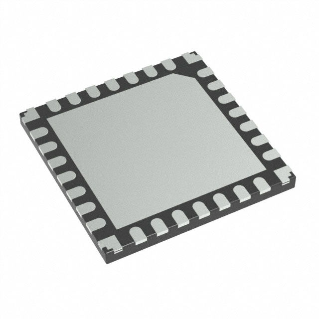
Pin Diagrams
RA1
RA2
RA3
RA4
AVDD
AVSS
VDD
VSS
RB0
RB1
RB2
RB3
RB4
RB5
1
2
3
4
5
6
7
8
9
10
11
12
13
14
dsPIC33CKXXXMP202
dsPIC33CKXXXMP502
28-Pin SSOP
28
27
26
25
24
23
22
21
20
19
18
17
16
15
RA0
MCLR
RB15
RB14
RB13
RB12
RB11
RB10
VDD
VSS
RB9
RB8
RB7
RB6
Note: Shaded pins are up to 5 VDC tolerant.
TABLE 3:
28-PIN SSOP(1)
Pin #
Function
Pin #
Function
1
OA1IN-/ANA1/RA1
15
PGC3/RP38/SCL2/RB6
2
OA1IN+/AN9/RA2
16
TDO/AN2/CMP3A/RP39/SDA3/RB7
3
DACOUT1/AN3/CMP1C/RA3
17
PGD1/AN10/RP40/SCL1/RB8
4
AN4/CMP3B/IBIAS3/RA4
18
PGC1/AN11/RP41/SDA1/RB9
5
AVDD
19
VSS
6
AVSS
20
VDD
7
VDD
21
TMS/RP42/PWM3H/RB10(2)
8
VSS
22
TCK/RP43/PWM3L/RB11
9
OSCI/CLKI/AN5/RP32/RB0
23
TDI/RP44/PWM2H/RB12
10
OSCO/CLKO/AN6/RP33/RB1(3)
24
RP45/PWM2L/RB13
11
OA2OUT/AN1/AN7/ANA0/CMP1D/CMP2D/CMP3D/RP34/
SCL3/INT0/RB2
25
RP46/PWM1H/RB14
12
PGD2/OA2IN-/AN8/RP35/RB3
26
RP47/PWM1L/RB15
13
PGC2/OA2IN+/RP36/RB4
27
MCLR
14
PGD3/RP37/SDA2/RB5
28
OA1OUT/AN0/CMP1A/IBIAS0/RA0
Note 1:
2:
3:
RPn represents remappable peripheral functions.
A pull-up resistor is connected to this pin when device is erased (JTAG enabled) and during programming.
This pin is toggled during programming.
2017-2021 Microchip Technology Inc.
DS70005349J-page 5
�dsPIC33CK256MP508 FAMILY
Pin Diagrams (Continued)
RB9
VSS
VDD
RB10
RB11
RB12
RB13
28-Pin UQFN(1,2)
28 27 26 25 24 23 22
RB14
1
21
RB8
RB15
2
20
RB7
MCLR
3
19
RB6
RA0
4
RA1
5
dsPIC33CKXXXMP502
dsPIC33CKXXXMP202 18
17
RA2
6
16
RB3
RA3
7
15
RB2
RB5
RB4
RB1
RB0
VSS
VDD
AVSS
RA4
AVDD
8 9 10 11 12 13 14
Note 1: Shaded pins are up to 5 VDC tolerant.
2: The large center pad on the bottom of the package may be left floating or connected to VSS. The four-corner
anchor pads are internally connected to the large bottom pad, and therefore, must be connected to the same
net as the large center pad.
TABLE 4:
28-PIN UQFN(1)
Pin #
Function
Pin #
Function
1
RP46/PWM1H/RB14
15
OA2OUT/AN1/AN7/ANA0/CMP1D/CMP2D/CMP3D/RP34/SCL3/INT0/RB2
2
RP47/PWM1L/RB15
16
PGD2/OA2IN-/AN8/RP35/RB3
3
MCLR
17
PGC2/OA2IN+/RP36/RB4
4
OA1OUT/AN0/CMP1A/IBIAS0/RA0
18
PGD3/RP37/SDA2/RB5
5
OA1IN-/ANA1/RA1
19
PGC3/RP38/SCL2/RB6
6
OA1IN+/AN9/RA2
20
TDO/AN2/CMP3A/RP39/SDA3/RB7
7
DACOUT1/AN3/CMP1C/RA3
21
PGD1/AN10/RP40/SCL1/RB8
8
AN4/CMP3B/IBIAS3/RA4
22
PGC1/AN11/RP41/SDA1/RB9
9
AVDD
23
VSS
10
AVSS
24
VDD
11
VDD
25
TMS/RP42/PWM3H/RB10(2)
12
VSS
26
TCK/RP43/PWM3L/RB11
13
OSCI/CLKI/AN5/RP32/RB0
27
TDI/RP44/PWM2H/RB12
14
OSCO/CLKO/AN6/RP33/RB1(3)
28
RP45/PWM2L/RB13
Note 1:
2:
3:
RPn represents remappable peripheral functions.
A pull-up resistor is connected to this pin when device is erased (JTAG enabled) and during programming.
This pin is toggled during programming.
DS70005349J-page 6
2017-2021 Microchip Technology Inc.
�dsPIC33CK256MP508 FAMILY
Pin Diagrams (Continued)
RB14
RB9
RC5
RC4
VSS
VDD
RB10
RB11
RB12
RB13
36-Pin UQFN(1,2)
1
36 35 34 33 32 31 30 29 28
27
RB8
RB7
RB15
2
26
MCLR
3
25
RB6
RC0
4
24
RB5
RA0
5
23
VDD
RA1
6
22
VSS
RA2
7
21
RB4
RA3
8
20
RB3
RA4
9
19
RB2
dsPIC33CKXXXMP503
dsPIC33CKXXXMP203
RB1
RB0
VSS
RC3
VDD
RC2
AVSS
RC1
AVDD
10 11 12 13 14 15 16 17 18
Note 1: Shaded pins are up to 5 VDC tolerant.
2: The large center pad on the bottom of the package may be left floating or connected to VSS. The four-corner
anchor pads are internally connected to the large bottom pad, and therefore, must be connected to the same
net as the large center pad.
TABLE 5:
36-PIN UQFN(1)
Pin #
Function
Pin #
Function
1
RP46/PWM1H/RB14
19
OA2OUT/AN1/AN7/ANA0/CMP1D/CMP2D/CMP3D/RP34/SCL3/INT0/RB2
2
RP47/PWM1L/RB15
20
PGD2/OA2IN-/AN8/RP35/RB3
3
MCLR
21
PGC2/OA2IN+/RP36/RB4
4
AN12/ANN0/RP48/RC0
22
VSS
5
OA1OUT/AN0/CMP1A/IBIAS0/RA0
23
VDD
6
OA1IN-/ANA1/RA1
24
PGD3/RP37/PWM6L/SDA2/RB5
7
OA1IN+/AN9/RA2
25
PGC3/RP38/PWM6H/SCL2/RB6
8
DACOUT1/AN3/CMP1C/RA3
26
TDO/AN2/CMP3A/RP39/SDA3/RB7
PGD1/AN10/RP40/SCL1/RB8
9
OA3OUT/AN4/CMP3B/IBIAS3/RA4
27
10
AVDD
28
PGC1/AN11/RP41/SDA1/RB9
11
AVSS
29
RP52/PWM5H/ASDA2/RC4
12
OA3IN-/AN13/CMP1B/ISRC0/RP49/RC1
30
RP53/PWM5L/ASCL2/RC5
13
OA3IN+/AN14/CMP2B/ISRC1/RP50/RC2
31
VSS
14
VDD
32
VDD
15
VSS
33
TMS/RP42/PWM3H/RB10(2)
16
AN15/CMP2A/IBIAS2/RP51/RC3
34
TCK/RP43/PWM3L/RB11
17
OSCI/CLKI/AN5/RP32/RB0
35
TDI/RP44/PWM2H/RB12
18
OSCO/CLKO/AN6/RP33/RB1(3)
36
RP45/PWM2L/RB13
Note 1:
2:
3:
RPn represents remappable peripheral functions.
A pull-up resistor is connected to this pin when device is erased (JTAG enabled) and during programming.
This pin is toggled during programming.
2017-2021 Microchip Technology Inc.
DS70005349J-page 7
�dsPIC33CK256MP508 FAMILY
Pin Diagrams (Continued)
RC4
RB9
RC5
RC10
RC11
VSS
VDD
RD1
RB10
RB11
RB12
RB13
48-Pin TQFP, UQFN(1,2)
48 47 46 45 44 43 42 41 40 39 38 37
RB14
1
36
RB8
RB15
2
35
RB7
RC12
RC13
3
34
RB6
4
33
RB5
MCLR
5
32
VDD
RD13
6
31
VSS
RC0
7
30
RA0
RA1
RA2
8
29
RD8
RC9
9
28
RC8
10
27
RB4
RA3
11
26
RB3
RA4
12
25
RB2
dsPIC33CKXXXMP505
dsPIC33CKXXXMP205
RC7
RD10
RB1
RB0
RC3
VSS
RC6
VDD
RC2
RC1
AVSS
AVDD
13 14 15 16 17 18 19 20 21 22 23 24
Note 1: Shaded pins are up to 5 VDC tolerant.
2: The large center pad on the bottom of the package may be left floating or connected to VSS. The four-corner
anchor pads are internally connected to the large bottom pad, and therefore, must be connected to the same
net as the large center pad.
DS70005349J-page 8
2017-2021 Microchip Technology Inc.
�dsPIC33CK256MP508 FAMILY
TABLE 6:
48-PIN TQFP, UQFN(1)
Pin #
Function
Pin #
Function
25
OA2OUT/AN1/AN7/ANA0/CMP1D/CMP2D/CMP3D/RP34/SCL3/INT0/RB2
1
RP46/PWM1H/RB14
2
RP47/PWM1L/RB15
26
PGD2/OA2IN-/AN8/RP35/RB3
3
RP60/PWM8H/RC12
27
PGC2/OA2IN+/RP36/RB4
4
RP61/PWM8L/RC13
28
RP56/ASDA1/SCK2/RC8
5
MCLR
29
RP57/ASCL1/SDI2/RC9
6
ANN2/RP77/RD13
30
RP72/SDO2/PCI19/RD8
7
AN12/ANN0/RP48/RC0
31
VSS
8
OA1OUT/AN0/CMP1A/IBIAS0/RA0
32
VDD
9
OA1IN-/ANA1/RA1
33
PGD3/RP37/PWM6L/SDA2/RB5
10
OA1IN+/AN9/RA2
34
PGC3/RP38/PWM6H/SCL2/RB6
11
DACOUT1/AN3/CMP1C/RA3
35
TDO/AN2/CMP3A/RP39/SDA3/RB7
12
OA3OUT/AN4/CMP3B/IBIAS3/RA4
36
PGD1/AN10/RP40/SCL1/RB8
13
AVDD
37
PGC1/AN11/RP41/SDA1/RB9
14
AVSS
38
RP52/PWM5H/ASDA2/RC4
15
OA3IN-/AN13/CMP1B/ISRC0/RP49/RC1
39
RP53/PWM5L/ASCL2/RC5
16
OA3IN+/AN14/CMP2B/ISRC1/RP50/RC2
40
RP58/PWM7H/RC10
17
AN17/ANN1/IBIAS1/RP54/RC6
41
RP59/PWM7L/RC11
18
VDD
42
VSS
19
VSS
43
VDD
20
AN15/CMP2A/IBIAS2/RP51/RC3
44
RP65/PWM4H/RD1
21
OSCI/CLKI/AN5/RP32/RB0
45
TMS/RP42/PWM3H/RB10(2)
22
OSCO/CLKO/AN6/RP33/RB1(3)
46
TCK/RP43/PWM3L/RB11
23
AN18/CMP3C/ISRC3/RP74/RD10
47
TDI/RP44/PWM2H/RB12
24
AN16/ISRC2/RP55/RC7
48
RP45/PWM2L/RB13
Note 1:
2:
3:
RPn represents remappable peripheral functions.
A pull-up resistor is connected to this pin when device is erased (JTAG enabled) and during programming.
This pin is toggled during programming.
2017-2021 Microchip Technology Inc.
DS70005349J-page 9
�dsPIC33CK256MP508 FAMILY
Pin Diagrams (Continued)
64
63
62
61
60
59
58
57
56
55
54
53
52
51
50
49
RB13
RB12
RB11
RB10
RD0
RD1
RD2
VDD
VSS
RD3
RD4
RC11
RC10
RC5
RC4
RB9
64-Pin TQFP, QFN
1
2
3
4
5
6
7
8
9
10
11
12
13
14
15
16
dsPIC33CKXXXMP506
dsPIC33CKXXXMP206
48
47
46
45
44
43
42
41
40
39
38
37
36
35
34
33
RB8
RB7
RB6
RB5
RD5
RD6
RD7
VDD
Vss
RD8
RD9
RC9
RC8
RB4
RB3
RB2
RA3
RA4
AVDD
AVSS
RD12
RC1
RC2
RC6
VDD
VSS
RC3
RB0
RB1
RD11
RD10
RC7
17
18
19
20
21
22
23
24
25
26
27
28
29
30
31
32
RB14
RB15
RC12
RC13
RC14
RC15
MCLR
RD15
VSS
VDD
RD14
RD13
RC0
RA0
RA1
RA2
Note: Shaded pins are up to 5 VDC tolerant.
DS70005349J-page 10
2017-2021 Microchip Technology Inc.
�dsPIC33CK256MP508 FAMILY
TABLE 7:
64-PIN TQFP, QFN(1)
Pin #
Function
Pin #
Function
1
RP46/PWM1H/PMD5/RB14
33
OA2OUT/AN1/AN7/ANA0/CMP1D/CMP2D/CMP3D/RP34/SCL3/INT0/RB2
2
RP47/PWM1L/PMD6/RB15
34
PGD2/OA2IN-/AN8/RP35/RB3
3
RP60/PWM8H/PMD7/RC12
35
PGC2/OA2IN+/RP36/RB4
4
RP61/PWM8L/PMA5/RC13
36
RP56/ASDA1/SCK2/RC8
5
RP62/PWM6H/PMA4/RC14
37
RP57/ASCL1/SDI2/RC9
6
RP63/PWM6L/PMA3/RC15
38
RP73/PCI20/RD9
7
MCLR
39
RP72/SDO2/PCI19/RD8
8
RP79/PCI22/PMA2/RD15
40
VSS
9
VSS
41
VDD
10
VDD
42
RP71/PMD15/RD7
11
RP78/PCI21/RD14
43
RP70/PMD14/RD6
12
ANN2/RP77/RD13
44
RP69/PMA15/PMCS2/RD5
13
AN12/ANN0/RP48/RC0
45
PGD3/RP37/SDA2/PMA14/PMCS1/PSCS/RB5
14
OA1OUT/AN0/CMP1A/IBIAS0/RA0
46
PGC3/RP38/SCL2/RB6
15
OA1IN-/ANA1/RA1
47
TDO/AN2/CMP3A/RP39/SDA3/RB7
16
OA1IN+/AN9/PMA6/RA2
48
PGD1/AN10/RP40/SCL1/RB8
17
DACOUT1/AN3/CMP1C/RA3
49
PGC1/AN11/RP41/SDA1/RB9
18
OA3OUT/AN4/CMP3B/IBIAS3/RA4
50
RP52/PWM5H/ASDA2/RC4
19
AVDD
51
RP53/PWM5L/ASCL2/PMWR/PMENB/PSWR/RC5
20
AVss
52
RP58/PWM7H/PMRD/PMWR/PSRD/RC10
21
RP76/RD12
53
RP59/PWM7L/RC11
22
OA3IN-/AN13/CMP1B/ISRC0/RP49/PMA7/RC1
54
RP68/ASDA3/RD4
23
OA3IN+/AN14/CMP2B/ISRC1/RP50/PMD13/PMA13/RC2
55
RP67/ASCL3/RD3
24
AN17/ANN1/IBIAS1/RP54/PMD12/PMA12/RC6
56
VSS
25
VDD
57
VDD
26
VSS
58
RP66/RD2
27
AN15/CMP2A/IBIAS2/RP51/PMD11/PMA11/RC3
59
RP65/PWM4H/RD1
28
OSCI/CLKI/AN5/RP32/PMD10/PMA10/RB0
60
RP64/PWM4L/PMD0/RD0
29
OSCO/CLKO/AN6/RP33/PMA1/PMALH/PSA1/RB1(3)
61
TMS/RP42/PWM3H/PMD1/RB10(2)
30
AN19/CMP2C/RP75/PMA0/PMALL/PSA0/RD11
62
TCK/RP43/PWM3L/PMD2/RB11
31
AN18/CMP3C/ISRC3/RP74/PMD9/PMA9/RD10
63
TDI/RP44/PWM2H/PMD3/RB12
32
AN16/ISRC2/RP55/PMD8/PMA8/RC7
64
RP45/PWM2L/PMD4/RB13
Note 1:
2:
3:
RPn represents remappable peripheral functions.
A pull-up resistor is connected to this pin when device is erased (JTAG enabled) and during programming.
This pin is toggled during programming.
2017-2021 Microchip Technology Inc.
DS70005349J-page 11
�dsPIC33CK256MP508 FAMILY
Pin Diagrams (Continued)
1
2
3
4
5
6
7
8
9
10
11
12
13
14
15
16
17
18
19
20
dsPIC33CKXXXMP508
dsPIC33CKXXXMP208
60
59
58
57
56
55
54
53
52
51
50
49
48
47
46
45
44
43
42
41
RB8
RE11
RB7
RE10
RB6
RB5
RD5
RD6
RD7
VDD
VSS
RD8
RD9
RC9
RC8
RB4
RE9
RB3
RE8
RB2
RA3
RE4
RA4
RE5
AVDD
AVSS
RD12
RC1
RC2
RC6
VDD
VSS
RC3
RB0
RB1
RD11
RE6
RD10
RE7
RC7
21
22
23
24
25
26
27
28
29
30
31
32
33
34
35
36
37
38
39
40
RB14
RE0
RB15
RE1
RC12
RC13
RC14
RC15
MCLR
RD15
VSS
VDD
RD14
RD13
RC0
RA0
RE2
RA1
RE3
RA2
80
79
78
77
76
75
74
73
72
71
70
69
68
67
66
65
64
63
62
61
RB13
RE15
RB12
RE14
RB11
RB10
RD0
RD1
RD2
VDD
VSS
RD3
RD4
RC11
RC10
RC5
RE13
RC4
RE12
RB9
80-Pin TQFP
Note: Shaded pins are up to 5 VDC tolerant.
DS70005349J-page 12
2017-2021 Microchip Technology Inc.
�dsPIC33CK256MP508 FAMILY
TABLE 8:
80-PIN TQFP(1)
Pin #
Function
Pin #
Function
1
RP46/PWM1H/PMD5/RB14
41
OA2OUT/AN1/AN7/ANA0/CMP1D/CMP2D/CMP3D/RP34/SCL3/INT0/RB2
2
AN20/RE0
42
RE8
3
RP47/PWM1L/PMD6/RB15
43
PGD2/OA2IN-/AN8/RP35/RB3
4
AN21/RE1
44
RE9
5
RP60/PWM8H/PMD7/RC12
45
PGC2/OA2IN+/RP36/RB4
6
RP61/PWM8L/PMA5/RC13
46
RP56/ASDA1/SCK2/RC8
7
RP62/PWM6H/PMA4/RC14
47
RP57/ASCL1/SDI2/RC9
8
RP63/PWM6L/PMA3/RC15
48
RP73/PCI20/RD9
9
MCLR
49
RP72/SDO2/PCI19/RD8
10
RP79/PCI22/PMA2/RD15
50
VSS
11
VSS
51
VDD
12
VDD
52
RP71/PMD15/RD7
13
RP78/PCI21/RD14
53
RP70/PMD14/RD6
14
ANN2/RP77/RD13
54
RP69/PMA15/PMCS2/RD5
15
AN12/ANN0/RP48/RC0
55
PGD3/RP37/SDA2/PMA14/PMCS1/PSCS/RB5
16
OA1OUT/AN0/CMP1A/IBIAS0/RA0
56
PGC3/RP38/SCL2/RB6
17
AN22/RE2
57
RE10
18
OA1IN-/ANA1/RA1
58
TDO/AN2/CMP3A/RP39/SDA3/RB7
19
AN23/RE3
59
RE11
20
OA1IN+/AN9/PMA6/RA2
60
PGD1/AN10/RP40/SCL1/RB8
21
DACOUT1/AN3/CMP1C/RA3
61
PGC1/AN11/RP41/SDA1/RB9
22
RE4
62
RE12
23
OA3OUT/AN4/CMP3B/IBIAS3/RA4
63
RP52/PWM5H/ASDA2/RC4
24
RE5
64
RE13
25
AVDD
65
RP53/PWM5L/ASCL2/PMWR/PMENB/PSWR/RC5
26
AVss
66
RP58/PWM7H/PMRD/PMWR/PSRD/RC10
27
RP76/RD12
67
RP59/PWM7L/RC11
28
OA3IN-/AN13/CMP1B/ISRC0/RP49/PMA7/RC1
68
RP68/ASDA3/RD4
29
OA3IN+/AN14/CMP2B/ISRC1/RP50/PMD13/PMA13/RC2
69
RP67/ASCL3/RD3
30
AN17/ANN1/IBIAS1/RP54/PMD12/PMA12/RC6
70
VSS
31
VDD
71
VDD
32
VSS
72
RP66/RD2
33
AN15/CMP2A/IBIAS2/RP51/PMD11/PMA11/RC3
73
RP65/PWM4H/RD1
34
OSCI/CLKI/AN5/RP32/PMD10/PMA10/RB0
74
RP64/PWM4L/PMD0/RD0
35
OSCO/CLKO/AN6/RP33/PMA1/PMALH/PSA1/RB1(3)
75
TMS/RP42/PWM3H/PMD1/RB10(2)
36
AN19/CMP2C/RP75/PMA0/PMALL/PSA0/RD11
76
TCK/RP43/PWM3L/PMD2/RB11
37
RE6
77
RE14
38
AN18/CMP3C/ISRC3/RP74/PMD9/PMA9/RD10
78
TDI/RP44/PWM2H/PMD3/RB12
39
RE7
79
RE15
40
AN16/ISRC2/RP55/PMD8/PMA8/RC7
80
RP45/PWM2L/PMD4/RB13
Note 1:
2:
3:
RPn represents remappable peripheral functions.
A pull-up resistor is connected to this pin when device is erased (JTAG enabled) and during programming.
This pin is toggled during programming.
2017-2021 Microchip Technology Inc.
DS70005349J-page 13
�dsPIC33CK256MP508 FAMILY
Table of Contents
1.0 Device Overview ........................................................................................................................................................................ 19
2.0 Guidelines for Getting Started with 16-Bit Digital Signal Controllers .......................................................................................... 25
3.0 CPU ............................................................................................................................................................................................ 31
4.0 Memory Organization ................................................................................................................................................................. 43
5.0 Flash Program Memory .............................................................................................................................................................. 81
6.0 Resets ........................................................................................................................................................................................ 97
7.0 Interrupt Controller ................................................................................................................................................................... 101
8.0 I/O Ports ................................................................................................................................................................................... 121
9.0 Oscillator with High-Frequency PLL ......................................................................................................................................... 185
10.0 Direct Memory Access (DMA) Controller ................................................................................................................................. 211
11.0 Controller Area Network (CAN FD) Module ............................................................................................................................. 221
12.0 High-Resolution PWM with Fine Edge Placement ................................................................................................................... 265
13.0 High-Speed, 12-Bit Analog-to-Digital Converter (ADC)............................................................................................................ 301
14.0 High-Speed Analog Comparator with Slope Compensation DAC ............................................................................................ 331
15.0 Quadrature Encoder Interface (QEI) ........................................................................................................................................ 343
16.0 Universal Asynchronous Receiver Transmitter (UART) ........................................................................................................... 363
17.0 Serial Peripheral Interface (SPI)............................................................................................................................................... 385
18.0 Inter-Integrated Circuit (I2C) ..................................................................................................................................................... 403
19.0 Parallel Master Port (PMP)....................................................................................................................................................... 413
20.0 Single-Edge Nibble Transmission (SENT) ............................................................................................................................... 427
21.0 Timer1 ...................................................................................................................................................................................... 437
22.0 Capture/Compare/PWM/Timer Modules (SCCP/MCCP) ......................................................................................................... 441
23.0 Configurable Logic Cell (CLC).................................................................................................................................................. 455
24.0 Peripheral Trigger Generator (PTG)......................................................................................................................................... 467
25.0 32-Bit Programmable Cyclic Redundancy Check (CRC) Generator ....................................................................................... 483
26.0 Current Bias Generator (CBG) ................................................................................................................................................. 487
27.0 Operational Amplifier ................................................................................................................................................................ 491
28.0 Deadman Timer (DMT) ........................................................................................................................................................... 495
29.0 Power-Saving Features ............................................................................................................................................................ 503
30.0 Special Features ...................................................................................................................................................................... 515
31.0 Instruction Set Summary .......................................................................................................................................................... 541
32.0 Development Support............................................................................................................................................................... 551
33.0 Electrical Characteristics .......................................................................................................................................................... 553
34.0 High-Temperature Electrical Characteristics ............................................................................................................................ 591
35.0 Packaging Information.............................................................................................................................................................. 601
Appendix A: Revision History............................................................................................................................................................. 627
Index ................................................................................................................................................................................................. 631
The Microchip Website....................................................................................................................................................................... 639
Customer Change Notification Service .............................................................................................................................................. 639
Customer Support .............................................................................................................................................................................. 639
Product Identification System............................................................................................................................................................. 641
DS70005349J-page 14
2017-2021 Microchip Technology Inc.
�dsPIC33CK256MP508 FAMILY
TO OUR VALUED CUSTOMERS
It is our intention to provide our valued customers with the best documentation possible to ensure successful use of your Microchip
products. To this end, we will continue to improve our publications to better suit your needs. Our publications will be refined and
enhanced as new volumes and updates are introduced.
If you have any questions or comments regarding this publication, please contact the Marketing Communications Department via
E-mail at docerrors@microchip.com. We welcome your feedback.
Most Current Data Sheet
To obtain the most up-to-date version of this data sheet, please register at our Worldwide Website at:
http://www.microchip.com
You can determine the version of a data sheet by examining its literature number found on the bottom outside corner of any page.
The last character of the literature number is the version number, (e.g., DS30000000A is version A of document DS30000000).
Errata
An errata sheet, describing minor operational differences from the data sheet and recommended workarounds, may exist for current
devices. As device/documentation issues become known to us, we will publish an errata sheet. The errata will specify the revision
of silicon and revision of document to which it applies.
To determine if an errata sheet exists for a particular device, please check with one of the following:
• Microchip’s Worldwide Website; http://www.microchip.com
• Your local Microchip sales office (see last page)
When contacting a sales office, please specify which device, revision of silicon and data sheet (include literature number) you are
using.
Customer Notification System
Register on our website at www.microchip.com to receive the most current information on all of our products.
2017-2021 Microchip Technology Inc.
DS70005349J-page 15
�dsPIC33CK256MP508 FAMILY
Referenced Sources
This device data sheet is based on the following
individual chapters of the “dsPIC33/PIC24 Family
Reference Manual”. These documents should be
considered as the general reference for the operation
of a particular module or device feature.
Note 1: To access the documents listed below,
browse to the documentation section of the
dsPIC33CK256MP508 product page of the
Microchip website (www.microchip.com) or
select a family reference manual section
from the following list.
In addition to parameters, features and
other documentation, the resulting page
provides links to the related family
reference manual sections.
•
•
•
•
•
•
•
•
•
•
•
•
•
•
•
•
•
•
•
•
•
•
•
•
•
•
•
•
•
•
•
•
“Introduction” (www.microchip.com/DS70573)
“Enhanced CPU” (www.microchip.com/DS70005158)
“dsPIC33/PIC24 Program Memory” (www.microchip.com/DS70000613)
“Data Memory” (www.microchip.com/DS70595)
“Dual Partition Flash Program Memory” (www.microchip.com/DS70005156)
“Flash Programming” (www.microchip.com/DS70000609)
“Reset” (www.microchip.com/DS70602)
“Interrupts” (www.microchip.com/DS70000600)
“I/O Ports with Edge Detect” (www.microchip.com/DS70005322)
“Oscillator Module with High-Speed PLL” (www.microchip.com/DS70005255)
“Direct Memory Access Controller (DMA)” (www.microchip.com/DS30009742)
“CAN Flexible Data-Rate (FD) Protocol Module” (www.microchip.com/DS70005340)
“High-Resolution PWM with Fine Edge Placement” (www.microchip.com/DS70005320)
“12-Bit High-Speed, Multiple SARs A/D Converter (ADC)” (www.microchip.com/DS70005213)
“High-Speed Analog Comparator Module with Slope Compensation DAC” (www.microchip.com/DS70005280)
“Quadrature Encoder Interface (QEI)” (www.microchip.com/DS70000601)
“Multiprotocol Universal Asynchronous Receiver Transmitter (UART) Module” (www.microchip.com/DS70005288)
“Serial Peripheral Interface (SPI) with Audio Codec Support” (www.microchip.com/DS70005136)
“Inter-Integrated Circuit (I2C)” (www.microchip.com/DS70000195)
“Parallel Master Port (PMP)” (www.microchip.com/DS70005344)
“Single-Edge Nibble Transmission (SENT) Module” (www.microchip.com/DS70005145)
“Timer1 Module” (www.microchip.com/DS70005279)
“Capture/Compare/PWM/Timer (MCCP and SCCP)” (www.microchip.com/DS30003035)
“Configurable Logic Cell (CLC)” (www.microchip.com/DS70005298)
“Peripheral Trigger Generator (PTG)” (www.microchip.com/DS70000669)
“32-Bit Programmable Cyclic Redundancy Check (CRC)” (www.microchip.com/DS30009729)
“Current Bias Generator (CBG)” (www.microchip.com/DS70005253)
“Deadman Timer” (www.microchip.com/DS70005155)
“Watchdog Timer and Power-Saving Modes” (www.microchip.com/DS70615)
“CodeGuard™ Intermediate Security” (www.microchip.com/DS70005182)
“Dual Watchdog Timer” (www.microchip.com/DS70005250)
“Programming and Diagnostics” (www.microchip.com/DS70608)
DS70005349J-page 16
2017-2021 Microchip Technology Inc.
�dsPIC33CK256MP508 FAMILY
Terminology Cross Reference
Table 9 provides updated terminology for depreciated
naming conventions. Register and bit names remain
unchanged, however, descriptions and usage guidance
may have been updated.
TABLE 9:
TERMINOLOGY CROSS
REFERENCES
Use Case
CPU
Deprecated
Term
Master
New Term
Initiator
DMA
Master
Initiator
I2C
Master
Host
SPI
PMP
UART, LIN mode
PWM
Slave
Client
Master
Host
Slave
Client
Master
Host
Slave
Client
Master
Commander
Slave
Responder
Master
Host
Slave
Client
2017-2021 Microchip Technology Inc.
DS70005349J-page 17
�dsPIC33CK256MP508 FAMILY
NOTES:
DS70005349J-page 18
2017-2021 Microchip Technology Inc.
�dsPIC33CK256MP508 FAMILY
1.0
DEVICE OVERVIEW
This document contains device-specific information
for the dsPIC33CK256MP508 Digital Signal Controller
(DSC) devices.
Note 1: This data sheet summarizes the features
of the dsPIC33CK256MP508 family of
devices. It is not intended to be a comprehensive resource. To complement the
information in this data sheet, refer to
the related section of the “dsPIC33/
PIC24 Family Reference Manual”,
which is available from the Microchip
website (www.microchip.com).
dsPIC33CK256MP508 devices contain extensive
Digital Signal Processor (DSP) functionality with a
high-performance, 16-bit MCU architecture.
Figure 1-1 shows a general block diagram of the core
and peripheral modules of the dsPIC33CK256MP508
family. Table 1-1 lists the functions of the various pins
shown in the pinout diagrams.
2: Some registers and associated bits
described in this section may not be available on all devices. Refer to Section 4.0
“Memory Organization” in this data
sheet for device-specific register and bit
information.
dsPIC33CK256MP508 FAMILY BLOCK DIAGRAM(1)
FIGURE 1-1:
CPU
Refer to Figure 3-1 for CPU diagram details.
PORTA(2)
16
PORTB(2)
OSC1/CLKI
Oscillator
Start-up
Timer
Timing
Generation
16
PORTC(2)
POR/BOR
MCLR
Watchdog
Timer
PORTD(2)
VDD, VSS
AVDD, AVSS
Peripheral Modules
PORTE(2)
PMP (1)
CLC (4)
QEI (2)
SENT (2)
CAN FD
(1)
ADC (1)
DMA (4)
SCCP (9)
2
I C (3)
Remappable
Pins(3)
OP AMP
(3)(4)
WDT/
DMT
CRC (1)
PTG (1)
HR PWM
(8)
Timer1
(1)
DAC/
Comparator
(3)
SPI/I2S
(3)
UART (3)
Ports
Note 1: The numbers in the parentheses are the number of instantiations of the module indicated.
2: Not all I/O pins or features are implemented on all device pinout configurations.
3: Some peripheral I/Os are only accessible through Peripheral Pin Select (PPS).
4: 28-lead devices have only two op amp instances.
2017-2021 Microchip Technology Inc.
DS70005349J-page 19
�dsPIC33CK256MP508 FAMILY
TABLE 1-1:
PINOUT I/O DESCRIPTIONS
Pin Name(1)
AN0-AN23
ANA0-ANA1
ANN0-ANN2
Pin Buffer
Type Type
I
I
I
Analog
Analog
Analog
PPS
No
No
No
Description
Analog input channels
Analog alternate inputs
Analog negative inputs
ADTRG31
I
ST
CLKI
I
No
CLKO
O
ST/
CMOS
—
Yes ADC Trigger Input 31
OSCI
I
No
OSCO
I/O
ST/
CMOS
—
REFCLKO
REFOI
O
I
—
ST
Yes Reference clock output
Yes Reference clock input
INT0
INT1
INT2
INT3
I
I
I
I
ST
ST
ST
ST
No
Yes
Yes
Yes
External Interrupt 0
External Interrupt 1
External Interrupt 2
External Interrupt 3
IOCA[4:0]
IOCB[15:0]
IOCC[15:0]
IOCD[15:0]
IOCE[15:0]
I
I
I
I
I
ST
ST
ST
ST
ST
No
No
No
No
No
Interrupt-on-Change input for PORTA
Interrupt-on-Change input for PORTB
Interrupt-on-Change input for PORTC
Interrupt-on-Change input for PORTD
Interrupt-on-Change input for PORTE
RP32-RP71
I/O
ST
Yes Remappable I/O ports
RA0-RA4
I/O
ST
No
PORTA is a bidirectional I/O port
RB0-RB15
I/O
ST
No
PORTB is a bidirectional I/O port
RC0-RC15
I/O
ST
No
PORTC is a bidirectional I/O port
RD0-RD15
I/O
ST
No
PORTD is a bidirectional I/O port
RE0-RE15
I/O
ST
No
PORTE is a bidirectional I/O port
T1CK
I
ST
Yes Timer1 external clock input
CAN1RX
CAN1TX
I
O
ST
—
Yes CAN1 receive input
Yes CAN1 transmit output
U1CTS
U1RTS
U1RX
U1TX
U1DSR
U1DTR
I
O
I
O
I
O
ST
—
ST
—
ST
—
Yes
Yes
Yes
Yes
Yes
Yes
No
No
External Clock (EC) source input. Always associated with OSCI pin
function.
Oscillator crystal output. Connects to crystal or resonator in Crystal
Oscillator mode. Optionally functions as CLKO in RC and EC
modes. Always associated with OSCO pin function.
Oscillator crystal input. ST buffer when configured in RC mode;
CMOS otherwise.
Oscillator crystal output. Connects to crystal or resonator in Crystal
Oscillator mode. Optionally functions as CLKO in RC and EC
modes.
UART1 Clear-to-Send
UART1 Request-to-Send
UART1 receive
UART1 transmit
UART1 Data-Set-Ready
UART1 Data-Terminal-Ready
Legend: CMOS = CMOS compatible input or output
Analog = Analog input
P = Power
ST = Schmitt Trigger input with CMOS levels
O = Output
I = Input
PPS = Peripheral Pin Select
TTL = TTL input buffer
DIG = Digital
Note 1: Not all pins are available in all package variants. See the “Pin Diagrams” section for pin availability.
2: PWM4L and PWM4H pins are available on PPS as well as dedicated.
3: SPI2 supports dedicated pins as well as PPS on 48, 64 and 80-pin devices.
4: Only 48, 64 and 80-pin devices have all eight PWM output pairs on dedicated pins. Refer to the “Pin
Diagrams” for PWM pin availability on other packages.
DS70005349J-page 20
2017-2021 Microchip Technology Inc.
�dsPIC33CK256MP508 FAMILY
TABLE 1-1:
PINOUT I/O DESCRIPTIONS (CONTINUED)
Pin Name(1)
Pin Buffer
Type Type
PPS
Description
U2CTS
U2RTS
U2RX
U2TX
U2DSR
U2DTR
I
O
I
O
I
O
ST
—
ST
—
ST
—
Yes
Yes
Yes
Yes
Yes
Yes
UART2 Clear-to-Send
UART2 Request-to-Send
UART2 receive
UART2 transmit
UART2 Data-Set-Ready
UART2 Data-Terminal-Ready
U3CTS
U3RTS
U3RX
U3TX
U3DSR
U3DTR
I
O
I
O
I
O
ST
—
ST
—
ST
—
Yes
Yes
Yes
Yes
Yes
Yes
UART3 Clear-to-Send
UART3 Request-to-Send
UART3 receive
UART3 transmit
UART3 Data-Set-Ready
UART3 Data-Terminal-Ready
SCK1
SDI1
SDO1
SS1
I/O
I
O
I/O
ST
ST
—
ST
Yes
Yes
Yes
Yes
Synchronous serial clock input/output for SPI1
SPI1 data in
SPI1 data out
SPI1 client synchronization or frame pulse I/O
SCK2
SDI2
SDO2
SS2
I/O
I
O
I/O
ST
ST
—
ST
Yes(3)
Yes(3)
Yes(3)
Yes(3)
Synchronous serial clock input/output for SPI2
SPI2 data in
SPI2 data out
SPI2 client synchronization or frame pulse I/O
SCK3
SDI3
SDO3
SS3
I/O
I
O
I/O
ST
ST
—
ST
Yes
Yes
Yes
Yes
Synchronous serial clock input/output for SPI3
SPI3 data in
SPI3 data out
SPI3 client synchronization or frame pulse I/O
SCL1
SDA1
ASCL1
ASDA1
I/O
I/O
I/O
I/O
ST
ST
ST
ST
No
No
No
No
Synchronous serial clock input/output for I2C1
Synchronous serial data input/output for I2C1
Alternate synchronous serial clock input/output for I2C1
Alternate synchronous serial data input/output for I2C1
SCL2
SDA2
ASCL2
ASDA2
I/O
I/O
I/O
I/O
ST
ST
ST
ST
No
No
No
No
Synchronous serial clock input/output for I2C2
Synchronous serial data input/output for I2C2
Alternate synchronous serial clock input/output for I2C2
Alternate synchronous serial data input/output for I2C2
SCL3
SDA3
ASCL3
ASDA3
I/O
I/O
I/O
I/O
ST
ST
ST
ST
No
No
No
No
Synchronous serial clock input/output for I2C3
Synchronous serial data input/output for I2C3
Alternate synchronous serial clock input/output for I2C3
Alternate synchronous serial data input/output for I2C3
QEIA1-QEIA2
QEIB1-QEIB2
QEINDX1-QEINDX2
QEIHOM1-QEIHOM2
QEICMP1-QEICMP2
I
I
I
I
O
ST
ST
ST
ST
—
Yes
Yes
Yes
Yes
Yes
QEI Inputs A1 and A2
QEI Inputs B1 and B2
QEI Index Inputs 1 and 2
QEI Home Inputs 1 and 2
QEI Comparator Outputs 1 and 2
SENT1-SENT2
SENT1OUT-SENT2OUT
I
O
ST
—
Yes SENT1 and SENT2 inputs
Yes SENT1 and SENT2 outputs
Legend: CMOS = CMOS compatible input or output
Analog = Analog input
P = Power
ST = Schmitt Trigger input with CMOS levels
O = Output
I = Input
PPS = Peripheral Pin Select
TTL = TTL input buffer
DIG = Digital
Note 1: Not all pins are available in all package variants. See the “Pin Diagrams” section for pin availability.
2: PWM4L and PWM4H pins are available on PPS as well as dedicated.
3: SPI2 supports dedicated pins as well as PPS on 48, 64 and 80-pin devices.
4: Only 48, 64 and 80-pin devices have all eight PWM output pairs on dedicated pins. Refer to the “Pin
Diagrams” for PWM pin availability on other packages.
2017-2021 Microchip Technology Inc.
DS70005349J-page 21
�dsPIC33CK256MP508 FAMILY
TABLE 1-1:
PINOUT I/O DESCRIPTIONS (CONTINUED)
Pin Name(1)
Pin Buffer
Type Type
PPS
Description
TMS
TCK
TDI
TDO
I
I
I
O
ST
ST
ST
—
No
No
No
No
JTAG Test mode select pin
JTAG test clock input pin
JTAG test data input pin
JTAG test data output pin
PCI8-PCI18
PCI19-PCI22
PWM1L-PWM8L(2)
PWM1H-PWM8H(2)
PWMEA-PWMED
I
I
O
O
O
ST
ST
—
—
—
Yes
No
No(4)
No(4)
Yes
CMP1A-CMP3A
CMP1B-CMP3B
CMP1C-CMP3C
CMP1D-CMP3D
I
I
I
I
Analog
Analog
Analog
Analog
No
No
No
No
Comparator Channels 1A through 3A inputs
Comparator Channels 1B through 3B inputs
Comparator Channels 1C through 3C inputs
Comparator Channels 1D through 3D inputs
DACOUT1
O
—
No
DAC output voltage
TCKI1-TCKI9
ICM1-ICM9
OCFA-OCFD
OCM1-OCM9
I
I
O
O
ST
ST
—
—
Yes
Yes
Yes
Yes
SCCP/MCCP Timer Inputs 1 through 9
SCCP/MCCP Capture Inputs 1 through 9
SCCP/MCCP Fault Inputs A through D
SCCP/MCCP Compare Outputs 1 through 9
IBIAS0-IBIAS3
ISRC0-ISRC3
O
O
Analog
Analog
No
No
50 µA Constant-Current Outputs 0 through 3
10 µA Constant-Current Outputs 0 through 3
OA1IN+
OA1INOA1OUT
OA2IN+
OA2INOA2OUT
OA3IN+
OA3INOA3OUT
I
I
O
I
I
O
I
I
O
—
—
—
—
—
—
—
—
—
No
No
No
No
No
No
No
No
No
Op Amp 1+ Input
Op Amp 1- Input
Op Amp 1 Output
Op Amp 2+ Input
Op Amp 2- Input
Op Amp 2 Output
Op Amp 3+ Input
Op Amp 3- Input
Op Amp 3 Output
PMA0/PMALL
PMA1/PMALH
PMA14/PMCS1
PMA15/PMCS2
PMA2-PMA13
PMD0-PMD15
PMRD/PMWR
PMWR/PMENB
PSA0
PSA1
PSCS
PSRD
PSWR
O
O
O
O
O
I/O
O
O
I
I
I
I
I
ST/TTL
ST/TTL
ST/TTL
ST/TTL
ST/TTL
ST/TTL
ST/TTL
ST/TTL
ST/TTL
ST/TTL
ST/TTL
ST/TTL
ST/TTL
No
No
No
No
No
No
No
No
No
No
No
No
No
PMP Address 0 or address latch low
PMP Address 1 or address latch high
PMP Address 14 or Chip Select 1
PMP Address 15 or Chip Select 2
PMP Address Lines 2-13
PMP Data Lines 0-15
PMP read or read/write signal
PMP write or data enable signal
PMP Client Address 0
PMP Client Address 1
PMP client chip select
PMP client read
PMP client write
CLCINA-CLCIND
CLC1OUT-CLC4OUT
I
O
ST
—
PWM PCI Inputs 8 through 18
PWM PCI Inputs 19 through 22
PWM Low Outputs 1 through 8
PWM High Outputs 1 through 8
PWM Event Outputs A through D
Yes CLC Inputs A through D
Yes CLC Outputs 1 through 4
Legend: CMOS = CMOS compatible input or output
Analog = Analog input
P = Power
ST = Schmitt Trigger input with CMOS levels
O = Output
I = Input
PPS = Peripheral Pin Select
TTL = TTL input buffer
DIG = Digital
Note 1: Not all pins are available in all package variants. See the “Pin Diagrams” section for pin availability.
2: PWM4L and PWM4H pins are available on PPS as well as dedicated.
3: SPI2 supports dedicated pins as well as PPS on 48, 64 and 80-pin devices.
4: Only 48, 64 and 80-pin devices have all eight PWM output pairs on dedicated pins. Refer to the “Pin
Diagrams” for PWM pin availability on other packages.
DS70005349J-page 22
2017-2021 Microchip Technology Inc.
�dsPIC33CK256MP508 FAMILY
TABLE 1-1:
PINOUT I/O DESCRIPTIONS (CONTINUED)
Pin Name(1)
Pin Buffer
Type Type
PPS
Description
Data I/O pin for Programming/Debugging Communication Channel 1
Clock input pin for Programming/Debugging Communication
Channel 1
Data I/O pin for Programming/Debugging Communication Channel 2
Clock input pin for Programming/Debugging Communication
Channel 2
Data I/O pin for Programming/Debugging Communication Channel 3
Clock input pin for Programming/Debugging Communication
Channel 3
PGD1
PGC1
I/O
I
ST
ST
No
No
PGD2
PGC2
I/O
I
ST
ST
No
No
PGD3
PGC3
I/O
I
ST
ST
No
No
MCLR
I/P
ST
No
Master Clear (Reset) input. This pin is an active-low Reset to the
device.
AVDD
P
P
No
Positive supply for analog modules. This pin must be connected at all
times.
AVSS
P
P
No
Ground reference for analog modules. This pin must be connected at
all times.
VDD
P
—
No
Positive supply for peripheral logic and I/O pins
VSS
P
—
No
Ground reference for logic and I/O pins
Legend: CMOS = CMOS compatible input or output
Analog = Analog input
P = Power
ST = Schmitt Trigger input with CMOS levels
O = Output
I = Input
PPS = Peripheral Pin Select
TTL = TTL input buffer
DIG = Digital
Note 1: Not all pins are available in all package variants. See the “Pin Diagrams” section for pin availability.
2: PWM4L and PWM4H pins are available on PPS as well as dedicated.
3: SPI2 supports dedicated pins as well as PPS on 48, 64 and 80-pin devices.
4: Only 48, 64 and 80-pin devices have all eight PWM output pairs on dedicated pins. Refer to the “Pin
Diagrams” for PWM pin availability on other packages.
2017-2021 Microchip Technology Inc.
DS70005349J-page 23
�dsPIC33CK256MP508 FAMILY
NOTES:
DS70005349J-page 24
2017-2021 Microchip Technology Inc.
�dsPIC33CK256MP508 FAMILY
2.2
RECOMMENDED
MINIMUM CONNECTION
0.1 µF
Ceramic
VDD
R
R1
MCLR
C
dsPIC33
0.1 µF
Ceramic
VSS
VDD
VDD
VSS
Decoupling Capacitors
The use of decoupling capacitors on every pair of
power supply pins, such as VDD, VSS, AVDD and
AVSS is required.
0.1 µF
Ceramic
2017-2021 Microchip Technology Inc.
0.1 µF
Ceramic
0.1 µF
Ceramic
L1(1)
Note 1:
Consider the following criteria when using decoupling
capacitors:
• Value and type of capacitor: Recommendation
of 0.1 µF (100 nF), 10-20V. This capacitor should
be a low-ESR and have resonance frequency in
the range of 20 MHz and higher. It is
recommended to use ceramic capacitors.
• Placement on the Printed Circuit Board: The
decoupling capacitors should be placed as close
to the pins as possible. It is recommended to
place the capacitors on the same side of the
board as the device. If space is constricted, the
capacitor can be placed on another layer on the
PCB using a via; however, ensure that the trace
length from the pin to the capacitor is within
one-quarter inch (6 mm) in length.
• Handling high-frequency noise: If the board is
experiencing high-frequency noise, above tens of
MHz, add a second ceramic-type capacitor in
parallel to the above described decoupling
capacitor. The value of the second capacitor can
be in the range of 0.01 µF to 0.001 µF. Place this
second capacitor next to the primary decoupling
capacitor. In high-speed circuit designs, consider
implementing a decade pair of capacitances as
close to the power and ground pins as possible.
For example, 0.1 µF in parallel with 0.001 µF.
VSS
• All VDD and VSS pins
(see Section 2.2 “Decoupling Capacitors”)
• All AVDD and AVSS pins
regardless if ADC module is not used (see
Section 2.2 “Decoupling Capacitors”)
• MCLR pin
(see Section 2.3 “Master Clear (MCLR) Pin”)
• PGCx/PGDx pins
used for In-Circuit Serial Programming™ (ICSP™)
and debugging purposes (see Section 2.4 “ICSP
Pins”)
• OSCI and OSCO pins
when an external oscillator source is used (see
Section 2.5 “External Oscillator Pins”)
FIGURE 2-1:
VSS
Getting started with the family devices of the
dsPIC33CK256MP508 requires attention to a minimal
set of device pin connections before proceeding with
development. The following is a list of pin names which
must always be connected:
VDD
Basic Connection Requirements
VDD
2.1
• Maximizing performance: On the board layout
from the power supply circuit, run the power and
return traces to the decoupling capacitors first,
and then to the device pins. This ensures that the
decoupling capacitors are first in the power chain.
Equally important is to keep the trace length
between the capacitor and the power pins to a
minimum, thereby reducing PCB track
inductance.
AVSS
GUIDELINES FOR GETTING
STARTED WITH 16-BIT DIGITAL
SIGNAL CONTROLLERS
AVDD
2.0
As an option, instead of a hard-wired connection, an
inductor (L1) can be substituted between VDD and
AVDD to improve ADC noise rejection. The inductor
impedance should be less than 1 and the inductor
capacity greater than 10 mA.
Where:
F CNV
f = ------------2
1
f = ---------------------- 2 LC
(i.e., ADC Conversion Rate/2)
2
1
L = ----------------------
2f C
2.2.1
BULK CAPACITORS
On boards with power traces running longer than six
inches in length, it is suggested to use a bulk capacitor
for integrated circuits, including DSCs, to supply a local
power source. The value of the bulk capacitor should
be determined based on the trace resistance that
connects the power supply source to the device and
the maximum current drawn by the device in the
application. In other words, select the bulk capacitor so
that it meets the acceptable voltage sag at the device.
Typical values range from 4.7 µF to 47 µF.
DS70005349J-page 25
�dsPIC33CK256MP508 FAMILY
2.3
Master Clear (MCLR) Pin
The MCLR
functions:
pin
provides
two
specific
device
• Device Reset
• Device Programming and Debugging.
During device programming and debugging, the
resistance and capacitance that can be added to the
pin must be considered. Device programmers and
debuggers drive the MCLR pin. Consequently,
specific voltage levels (VIH and VIL) and fast signal
transitions must not be adversely affected. Therefore,
specific values of R and C will need to be adjusted
based on the application and PCB requirements.
For example, as shown in Figure 2-2, it is
recommended that the capacitor, C, be isolated from
the MCLR pin during programming and debugging
operations.
Place the components, as shown in Figure 2-2,
within one-quarter inch (6 mm) from the MCLR pin.
FIGURE 2-2:
EXAMPLE OF MCLR PIN
CONNECTIONS
VDD
R(1)
R1(2)
MCLR
JP
dsPIC33
C
Note 1: R 10 k is recommended. A suggested
starting value is 10 k. Ensure that the
MCLR pin VIH and VIL specifications are met.
2: R1 470 will limit any current flowing into
MCLR from the external capacitor, C, in the
event of MCLR pin breakdown due to
Electrostatic Discharge (ESD) or Electrical
Overstress (EOS). Ensure that the MCLR pin
VIH and VIL specifications are met.
2.4
Pull-up resistors, series diodes and capacitors on the
PGCx and PGDx pins are not recommended as they
will interfere with the programmer/debugger communications to the device. If such discrete components are
an application requirement, they should be removed
from the circuit during programming and debugging.
Alternatively, refer to the AC/DC characteristics and
timing requirements information in the respective
device Flash programming specification for information
on capacitive loading limits and pin Voltage Input High
(VIH) and Voltage Input Low (VIL) requirements.
Ensure that the “Communication Channel Select” (i.e.,
PGCx/PGDx pins) programmed into the device
matches the physical connections for the ICSP to the
programmer/debugger.
For more information regarding Microchip’s programmers
and debuggers, refer to Section 32.0 “Development
Support”.
2.5
External Oscillator Pins
When the Primary Oscillator (POSC) circuit is used to
connect a crystal oscillator, special care and consideration is needed to ensure proper operation. The
POSC circuit should be tested across the environmental conditions that the end product is intended to
be used. The load capacitors specified in the crystal
oscillator data sheet can be used as a starting point,
however, the parasitic capacitance from the PCB
traces can affect the circuit, and the values may need
to be altered to ensure proper start-up and operation.
Excessive trace length and other physical interaction
can lead to poor signal quality. Poorly tuned oscillator
circuits can have reduced amplitude, incorrect
frequency (runt pulses), distorted waveforms and long
start-up times that may result in unpredictable application behavior, such as instruction misexecution, illegal
op code fetch, etc. Ensure that the crystal oscillator
circuit is at full amplitude and correct frequency before
the system begins to execute code. In planning the
application’s routing and I/O assignments, ensure that
adjacent port pins, and other signals in close proximity
to the oscillator do not have high frequencies, short
rise and fall times and other similar noise. For further
information on the primary oscillator see Section 9.4
“Primary Oscillator (POSC)”.
ICSP Pins
The PGCx and PGDx pins are used for ICSP and
debugging purposes. It is recommended to keep the
trace length between the ICSP connector and the ICSP
pins on the device as short as possible. If the ICSP connector is expected to experience an ESD event, a
series resistor is recommended, with the value in the
range of a few tens of Ohms, not to exceed 100 Ohms.
DS70005349J-page 26
2017-2021 Microchip Technology Inc.
�dsPIC33CK256MP508 FAMILY
2.6
External Oscillator Layout
Guidance
Use best practices during PCB layout to ensure
robust start-up and operation. The oscillator circuit
should be placed on the same side of the board as
the device. Also, place the oscillator circuit close to
the respective oscillator pins, not exceeding one-half
inch (12 mm) distance between them. The load
capacitors should be placed next to the oscillator
itself, on the same side of the board. Use a grounded
copper pour around the oscillator circuit to isolate
them from surrounding circuits. The grounded copper
pour should be routed directly to the MCU ground. Do
not run any signal traces or power traces inside the
ground pour. If using a two-sided board, avoid any
traces on the other side of the board where the crystal
is placed. Suggested layouts are shown in Figure 2-3.
With fine-pitch packages, it is not always possible to
completely surround the pins and components. A suitable solution is to tie the broken guard sections to a
mirrored ground layer. In all cases, the guard trace(s)
must be returned to ground.
For additional information and design guidance on
oscillator circuits, please refer to these Microchip
Application Notes, available at the Microchip website
(www.microchip.com):
• AN943, “Practical PICmicro® Oscillator Analysis
and Design”
• AN949, “Making Your Oscillator Work”
• AN1798, “Crystal Selection for Low-Power
Secondary Oscillator
FIGURE 2-3:
SUGGESTED
PLACEMENT OF THE
OSCILLATOR CIRCUIT
Single-Sided and In-Line Layouts:
Copper Pour
(tied to ground)
Primary Oscillator
Crystal
DEVICE PINS
Primary
Oscillator
OSCI
C1
`
OSCO
GND
C2
`
Fine-Pitch (Dual-Sided) Layouts:
Top Layer Copper Pour
(tied to ground)
Bottom Layer
Copper Pour
(tied to ground)
OSCO
C2
Oscillator
Crystal
GND
C1
OSCI
DEVICE PINS
2017-2021 Microchip Technology Inc.
DS70005349J-page 27
�dsPIC33CK256MP508 FAMILY
2.7
Oscillator Value Conditions on
Device Start-up
2.9
• Power Factor Correction (PFC):
- Interleaved PFC
- Critical Conduction PFC
- Bridgeless PFC
• DC/DC Converters:
- Buck, Boost, Forward, Flyback, Push-Pull
- Half/Full-Bridge
- Phase-Shift Full-Bridge
- Resonant Converters
• DC/AC:
- Half/Full-Bridge Inverter
- Resonant Inverter
• Motor Control
- BLDC
- PMSM
- SR
- ACIM
If the PLL of the target device is enabled and
configured for the device start-up oscillator, the
maximum oscillator source frequency must be limited
to a certain frequency (see Section 9.0 “Oscillator
with High-Frequency PLL”) to comply with device
PLL start-up conditions. This means that if the external
oscillator frequency is outside this range, the application must start up in the FRC mode first. The default
PLL settings after a POR with an oscillator frequency
outside this range will violate the device operating
speed.
Once the device powers up, the application firmware
can initialize the PLL SFRs, CLKDIV and PLLFBD, to a
suitable value, and then perform a clock switch to the
Oscillator + PLL clock source. Note that clock switching
must be enabled in the device Configuration Word.
2.8
Targeted Applications
Unused I/Os
Examples of typical application connections are shown
in Figure 2-4 through Figure 2-6.
Unused I/O pins should be configured as outputs and
driven to a logic low state.
Alternatively, connect a 1k to 10k resistor between VSS
and unused pins, and drive the output to logic low.
FIGURE 2-4:
INTERLEAVED PFC
VOUT+
|VAC|
k2
k1
k4
VAC
k3
VOUTFET
Driver
FET
Driver
ADC Channel
PWM
ADC
Channel
PWM
ADC
Channel
ADC
Channel
dsPIC33CK256MP508
ADC Channel
DS70005349J-page 28
2017-2021 Microchip Technology Inc.
�dsPIC33CK256MP508 FAMILY
FIGURE 2-5:
PHASE-SHIFTED FULL-BRIDGE CONVERTER
VIN+
Gate 6
Gate 3
Gate 1
VOUT+
S1
S3
VOUT-
Gate 2
Gate 4
Gate 5
Gate 6
Gate 5
VIN-
FET
Driver
k2
PWM
ADC
Channel
k1
Analog
Ground
Gate 1
S1
FET
Driver
PWM
Gate 3
S3
FET
Driver
ADC
Channel
dsPIC33CK256MP508
PWM
Gate 2
Gate 4
2017-2021 Microchip Technology Inc.
DS70005349J-page 29
�dsPIC33CK256MP508 FAMILY
FIGURE 2-6:
OFF-LINE UPS
VDC
Push-Pull Converter
Full-Bridge Inverter
VOUT+
VBAT
+
VOUTGND
GND
FET
Driver
FET
Driver
PWM
PWM
k2
k1
ADC
ADC
or
Analog Comp.
k3
FET
Driver
FET
Driver
FET
Driver
FET
Driver
PWM
PWM
PWM
PWM
dsPIC33CK256MP508
ADC
k4
k5
ADC
ADC
ADC
PWM
FET
Driver
k6
+
Battery Charger
DS70005349J-page 30
2017-2021 Microchip Technology Inc.
�dsPIC33CK256MP508 FAMILY
3.0
CPU
Note 1: This data sheet summarizes the features
of the dsPIC33CK256MP508 family of
devices. It is not intended to be a comprehensive reference source. To complement
the information in this data sheet, refer to
“Enhanced CPU” (www.microchip.com/
DS70005158) in the “dsPIC33/PIC24
Family Reference Manual”.
2: Some registers and associated bits
described in this section may not be
available on all devices. Refer to
Section 4.0 “Memory Organization” in
this data sheet for device-specific register
and bit information.
The dsPIC33CK256MP508 family CPU has a 16-bit
(data) modified Harvard architecture with an enhanced
instruction set, including significant support for Digital
Signal Processing (DSP). The CPU has a 24-bit instruction word with a variable length opcode field. The
Program Counter (PC) is 23 bits wide and addresses up
to 4M x 24 bits of user program memory space.
An instruction prefetch mechanism helps maintain
throughput and provides predictable execution. Most
instructions execute in a single-cycle effective execution rate, with the exception of instructions that change
the program flow, the double-word move (MOV.D)
instruction, PSV accesses and the table instructions.
Overhead-free program loop constructs are supported
using the DO and REPEAT instructions, both of which
are interruptible at any point.
3.1
Registers
The dsPIC33CK256MP508 devices have sixteen, 16-bit
Working registers in the programmer’s model. Each of
the Working registers can act as a Data, Address or
Address Offset register. The 16th Working register
(W15) operates as a Software Stack Pointer for
interrupts and calls.
In addition, the dsPIC33CK256MP508 devices include
four Alternate Working register sets, which consist of W0
through W14. The Alternate Working registers can be
made persistent to help reduce the saving and restoring
of register content during Interrupt Service Routines
(ISRs). The Alternate Working registers can be assigned
to a specific Interrupt Priority Level (IPL1 through IPL6) by
configuring the CTXTx[2:0] bits in the FALTREG Configuration register. The Alternate Working registers can also
be accessed manually by using the CTXTSWP instruction.
The CCTXI[2:0] and MCTXI[2:0] bits in the CTXTSTAT
register can be used to identify the current, and most
recent, manually selected Working register sets.
2017-2021 Microchip Technology Inc.
3.2
Instruction Set
The instruction set for dsPIC33CK256MP508 devices
has two classes of instructions: the MCU class of
instructions and the DSP class of instructions. These
two instruction classes are seamlessly integrated into the
architecture and execute from a single execution unit.
The instruction set includes many addressing modes and
was designed for optimum C compiler efficiency.
3.3
Data Space Addressing
The base Data Space can be addressed as up to
4K words or 8 Kbytes, and is split into two blocks,
referred to as X and Y data memory. Each memory block
has its own independent Address Generation Unit
(AGU). The MCU class of instructions operates solely
through the X memory AGU, which accesses the entire
memory map as one linear Data Space. Certain DSP
instructions operate through the X and Y AGUs to support dual operand reads, which splits the data address
space into two parts. The X and Y Data Space boundary
is device-specific.
The upper 32 Kbytes of the Data Space memory map
can optionally be mapped into Program Space (PS) at
any 16K program word boundary. The program-to-Data
Space mapping feature, known as Program Space
Visibility (PSV), lets any instruction access Program
Space as if it were Data Space. Refer to “Data
Memory” (DS70595) in the “dsPIC33/PIC24 Family
Reference Manual” for more details on PSV and table
accesses.
On dsPIC33CK256MP508 family devices, overheadfree circular buffers (Modulo Addressing) are
supported in both X and Y address spaces. The
Modulo Addressing removes the software boundary
checking overhead for DSP algorithms. The X AGU
Circular Addressing can be used with any of the MCU
class of instructions. The X AGU also supports BitReversed Addressing to greatly simplify input or output
data re-ordering for radix-2 FFT algorithms.
3.4
Addressing Modes
The CPU supports these addressing modes:
•
•
•
•
•
•
Inherent (no operand)
Relative
Literal
Memory Direct
Register Direct
Register Indirect
Each instruction is associated with a predefined
addressing mode group, depending upon its functional
requirements. As many as six addressing modes are
supported for each instruction.
DS70005349J-page 31
�dsPIC33CK256MP508 FAMILY
FIGURE 3-1:
dsPIC33CK256MP508 FAMILY CPU BLOCK DIAGRAM
X Address Bus
Y Data Bus
X Data Bus
Interrupt
Controller
PSV and Table
Data Access
24 Control Block
8
Data Latch
Data Latch
Y Data
RAM
X Data
RAM
Address
Latch
Address
Latch
16
Y Address Bus
24
24
PCU PCH PCL
Program Counter
Loop
Stack
Control
Control
Logic
Logic
Address Latch
16
16
16
16
16
16
24
16
X RAGU
X WAGU
16
Y AGU
Program Memory
EA MUX
16
Data Latch
24
16
Literal Data
IR
24
ROM Latch
16
16
16-Bit
Working Register Arrays
16
16
16
Divide
Support
DSP
Engine
16-Bit ALU
Control Signals
to Various Blocks
Instruction
Decode and
Control
Power, Reset
and Oscillator
Modules
16
16
Ports
Peripheral
Modules
DS70005349J-page 32
2017-2021 Microchip Technology Inc.
�dsPIC33CK256MP508 FAMILY
3.4.1
PROGRAMMER’S MODEL
The programmer’s model for the dsPIC33CK256MP508
family is shown in Figure 3-2. All registers in the
programmer’s model are memory-mapped and can be
manipulated directly by instructions. Table 3-1 lists a
description of each register.
TABLE 3-1:
In addition to the registers contained in the programmer’s
model, the dsPIC33CK256MP508 devices contain
control registers for Modulo Addressing, Bit-Reversed
Addressing and interrupts. These registers are described
in subsequent sections of this document.
All registers associated with the programmer’s model
are memory-mapped, as shown in Figure 3-2.
PROGRAMMER’S MODEL REGISTER DESCRIPTIONS
Register(s) Name
Description
W0 through W15(1)
Working Register Array
W0 through W14(1)
Alternate Working Register Array 1
W14(1)
Alternate Working Register Array 2
W0 through W14(1)
Alternate Working Register Array 3
(1)
Alternate Working Register Array 4
W0 through
W0 through W14
ACCA, ACCB
40-Bit DSP Accumulators (Additional 4 Alternate Accumulators)
PC
23-Bit Program Counter
SR
ALU and DSP Engine STATUS Register
SPLIM
Stack Pointer Limit Value Register
TBLPAG
Table Memory Page Address Register
DSRPAG
Extended Data Space (EDS) Read Page Register
RCOUNT
REPEAT Loop Counter Register
DCOUNT
DO Loop Counter Register
DOSTARTH, DOSTARTL(2)
DO Loop Start Address Register (High and Low)
DOENDH, DOENDL
DO Loop End Address Register (High and Low)
CORCON
Contains DSP Engine, DO Loop Control and Trap Status bits
Note 1:
2:
Memory-mapped W0 through W14 represent the value of the register in the currently active CPU context.
The DOSTARTH and DOSTARTL registers are read-only.
2017-2021 Microchip Technology Inc.
DS70005349J-page 33
�dsPIC33CK256MP508 FAMILY
FIGURE 3-2:
PROGRAMMER’S MODEL
D15
D0
D15
D0
D15
D0
D15
D0
D15
D0
W0 (WREG)
W1
W0-W3
W0
W1
W0 W0 W0
W1 W1 W1
W4
W2
W3
W4
W2 W2 W2
W3 W3 W3
W4 W4 W4
W5
W5
W5 W5 W5
W6
W7
W6
W7
W6
W7
W6 W6
W7 W7
W8
W8
W8
W8 W8
W9
W9
W9
W9 W9
W2
W3
DSP Operand
Registers
Working/Address
Registers
DSP Address
Registers
W10 W10
W11 W11
W12 W12
W13 W13
W10 W10 W10
W11 W11 W11
Frame Pointer/W14 W14
W14 W14 W14
Alternate
Working/Address
Registers
W12 W12 W12
W13 W13 W13
Stack Pointer/W15 0
PUSH.S and POP.S Shadows
SPLIM
Nested DO Stack
AD39
AD15
AD31
AD39
AD15
AD31
AD39
AD0
AD0
AD0
AD15
AD31
AD39
DSP
Accumulators(1)
Stack Pointer Limit
0
AD31
AD39
AD15
AD31
AD0
AD0
AD15
ACCA
ACCB
PC23
PC0
0
0
Program Counter
0
7
TBLPAG
Data Table Page Address
9
0
DSRPAG
X Data Space Read Page Address
15
0
REPEAT Loop Counter
RCOUNT
15
0
DCOUNT
DO Loop Counter and Stack
23
0
DOSTART
0
0
DO Loop Start Address and Stack
23
0
DOEND
0
0
DO Loop End Address and Stack
15
0
CORCON
CPU Core Control Register
SRL
OA
OB
SA
DS70005349J-page 34
SB
OAB
SAB
DA DC IPL2 IPL1 IPL0 RA
N
OV
Z
C
STATUS Register
2017-2021 Microchip Technology Inc.
�dsPIC33CK256MP508 FAMILY
3.4.2
CPU RESOURCES
Many useful resources are provided on the main product page of the Microchip website for the devices listed
in this data sheet. This product page contains the latest
updates and additional information.
2017-2021 Microchip Technology Inc.
3.4.2.1
Key Resources
• “Enhanced CPU” (DS70005158) in the
“dsPIC33/PIC24 Family Reference Manual”
• Code Samples
• Application Notes
• Software Libraries
• Webinars
• All related “dsPIC33/PIC24 Family Reference
Manual” Sections
• Development Tools
DS70005349J-page 35
�dsPIC33CK256MP508 FAMILY
3.4.3
CPU CONTROL REGISTERS
REGISTER 3-1:
SR: CPU STATUS REGISTER
R/W-0
R/W-0
R/W-0
OB
SA(3)
OA
R/W-0
(3)
SB
R/C-0
R/C-0
R-0
R/W-0
OAB
SAB
DA
DC
bit 15
bit 8
R/W-0(2)
R/W-0(2)
(1)
IPL2
IPL1
(1)
R/W-0(2)
IPL0
(1)
R-0
R/W-0
R/W-0
R/W-0
R/W-0
RA
N
OV
Z
C
bit 7
bit 0
Legend:
C = Clearable bit
R = Readable bit
W = Writable bit
U = Unimplemented bit, read as ‘0’
-n = Value at POR
‘1’= Bit is set
‘0’ = Bit is cleared
x = Bit is unknown
bit 15
OA: Accumulator A Overflow Status bit
1 = Accumulator A has overflowed
0 = Accumulator A has not overflowed
bit 14
OB: Accumulator B Overflow Status bit
1 = Accumulator B has overflowed
0 = Accumulator B has not overflowed
bit 13
SA: Accumulator A Saturation ‘Sticky’ Status bit(3)
1 = Accumulator A is saturated or has been saturated at some time
0 = Accumulator A is not saturated
bit 12
SB: Accumulator B Saturation ‘Sticky’ Status bit(3)
1 = Accumulator B is saturated or has been saturated at some time
0 = Accumulator B is not saturated
bit 11
OAB: OA || OB Combined Accumulator Overflow Status bit
1 = Accumulator A or B has overflowed
0 = Neither Accumulator A or B has overflowed
bit 10
SAB: SA || SB Combined Accumulator ‘Sticky’ Status bit
1 = Accumulator A or B is saturated or has been saturated at some time
0 = Neither Accumulator A or B is saturated
bit 9
DA: DO Loop Active bit
1 = DO loop is in progress
0 = DO loop is not in progress
bit 8
DC: MCU ALU Half Carry/Borrow bit
1 = A carry-out from the 4th low-order bit (for byte-sized data) or 8th low-order bit (for word-sized data)
of the result occurred
0 = No carry-out from the 4th low-order bit (for byte-sized data) or 8th low-order bit (for word-sized
data) of the result occurred
Note 1:
2:
3:
The IPL[2:0] bits are concatenated with the IPL[3] bit (CORCON[3]) to form the CPU Interrupt Priority
Level. The value in parentheses indicates the IPL, if IPL[3] = 1. User interrupts are disabled when
IPL[3] = 1.
The IPL[2:0] Status bits are read-only when the NSTDIS bit (INTCON1[15]) = 1.
A data write to the SR register can modify the SA and SB bits by either a data write to SA and SB or by
clearing the SAB bit. To avoid a possible SA or SB bit write race condition, the SA and SB bits should not
be modified using bit operations.
DS70005349J-page 36
2017-2021 Microchip Technology Inc.
�dsPIC33CK256MP508 FAMILY
REGISTER 3-1:
SR: CPU STATUS REGISTER (CONTINUED)
bit 7-5
IPL[2:0]: CPU Interrupt Priority Level Status bits(1,2)
111 = CPU Interrupt Priority Level is 7 (15); user interrupts are disabled
110 = CPU Interrupt Priority Level is 6 (14)
101 = CPU Interrupt Priority Level is 5 (13)
100 = CPU Interrupt Priority Level is 4 (12)
011 = CPU Interrupt Priority Level is 3 (11)
010 = CPU Interrupt Priority Level is 2 (10)
001 = CPU Interrupt Priority Level is 1 (9)
000 = CPU Interrupt Priority Level is 0 (8)
bit 4
RA: REPEAT Loop Active bit
1 = REPEAT loop is in progress
0 = REPEAT loop is not in progress
bit 3
N: MCU ALU Negative bit
1 = Result was negative
0 = Result was non-negative (zero or positive)
bit 2
OV: MCU ALU Overflow bit
This bit is used for signed arithmetic (two’s complement). It indicates an overflow of the magnitude that
causes the sign bit to change state.
1 = Overflow occurred for signed arithmetic (in this arithmetic operation)
0 = No overflow occurred
bit 1
Z: MCU ALU Zero bit
1 = An operation that affects the Z bit has set it at some time in the past
0 = The most recent operation that affects the Z bit has cleared it (i.e., a non-zero result)
bit 0
C: MCU ALU Carry/Borrow bit
1 = A carry-out from the Most Significant bit of the result occurred
0 = No carry-out from the Most Significant bit of the result occurred
Note 1:
2:
3:
The IPL[2:0] bits are concatenated with the IPL[3] bit (CORCON[3]) to form the CPU Interrupt Priority
Level. The value in parentheses indicates the IPL, if IPL[3] = 1. User interrupts are disabled when
IPL[3] = 1.
The IPL[2:0] Status bits are read-only when the NSTDIS bit (INTCON1[15]) = 1.
A data write to the SR register can modify the SA and SB bits by either a data write to SA and SB or by
clearing the SAB bit. To avoid a possible SA or SB bit write race condition, the SA and SB bits should not
be modified using bit operations.
2017-2021 Microchip Technology Inc.
DS70005349J-page 37
�dsPIC33CK256MP508 FAMILY
REGISTER 3-2:
CORCON: CORE CONTROL REGISTER
R/W-0
U-0
R/W-0
R/W-0
R/W-0
R-0
R-0
R-0
VAR
—
US1
US0
EDT(1)
DL2
DL1
DL0
bit 15
bit 8
R/W-0
R/W-0
R/W-1
R/W-0
R/C-0
R-0
R/W-0
R/W-0
SATA
SATB
SATDW
ACCSAT
IPL3(2)
SFA
RND
IF
bit 7
bit 0
Legend:
C = Clearable bit
R = Readable bit
W = Writable bit
U = Unimplemented bit, read as ‘0’
-n = Value at POR
‘1’ = Bit is set
‘0’ = Bit is cleared
x = Bit is unknown
bit 15
VAR: Variable Exception Processing Latency Control bit
1 = Variable exception processing latency is enabled
0 = Fixed exception processing latency is enabled
bit 14
Unimplemented: Read as ‘0’
bit 13-12
US[1:0]: DSP Multiply Unsigned/Signed Control bits
11 = Reserved
10 = DSP engine multiplies are mixed sign
01 = DSP engine multiplies are unsigned
00 = DSP engine multiplies are signed
bit 11
EDT: Early DO Loop Termination Control bit(1)
1 = Terminates executing DO loop at the end of the current loop iteration
0 = No effect
bit 10-8
DL[2:0]: DO Loop Nesting Level Status bits
111 = Seven DO loops are active
...
001 = One DO loop is active
000 = Zero DO loops are active
bit 7
SATA: ACCA Saturation Enable bit
1 = Accumulator A saturation is enabled
0 = Accumulator A saturation is disabled
bit 6
SATB: ACCB Saturation Enable bit
1 = Accumulator B saturation is enabled
0 = Accumulator B saturation is disabled
bit 5
SATDW: Data Space Write from DSP Engine Saturation Enable bit
1 = Data Space write saturation is enabled
0 = Data Space write saturation is disabled
bit 4
ACCSAT: Accumulator Saturation Mode Select bit
1 = 9.31 saturation (super saturation)
0 = 1.31 saturation (normal saturation)
bit 3
IPL3: CPU Interrupt Priority Level Status bit 3(2)
1 = CPU Interrupt Priority Level is greater than 7
0 = CPU Interrupt Priority Level is 7 or less
Note 1:
2:
This bit is always read as ‘0’.
The IPL3 bit is concatenated with the IPL[2:0] bits (SR[7:5]) to form the CPU Interrupt Priority Level.
DS70005349J-page 38
2017-2021 Microchip Technology Inc.
�dsPIC33CK256MP508 FAMILY
REGISTER 3-2:
CORCON: CORE CONTROL REGISTER (CONTINUED)
bit 2
SFA: Stack Frame Active Status bit
1 = Stack frame is active; W14 and W15 address 0x0000 to 0xFFFF, regardless of DSRPAG
0 = Stack frame is not active; W14 and W15 address the base Data Space
bit 1
RND: Rounding Mode Select bit
1 = Biased (conventional) rounding is enabled
0 = Unbiased (convergent) rounding is enabled
bit 0
IF: Integer or Fractional Multiplier Mode Select bit
1 = Integer mode is enabled for DSP multiply
0 = Fractional mode is enabled for DSP multiply
Note 1:
2:
This bit is always read as ‘0’.
The IPL3 bit is concatenated with the IPL[2:0] bits (SR[7:5]) to form the CPU Interrupt Priority Level.
REGISTER 3-3:
MSTRPR: EDS BUS INITIATOR PRIORITY CONTROL REGISTER
U-0
U-0
U-0
U-0
U-0
U-0
U-0
U-0
—
—
—
—
—
—
—
—
bit 15
bit 8
U-0
U-0
R/W-0
R/W-0
U-0
U-0
U-0
R/W-0
—
—
DMAPR
CANPR
—
—
—
NVMPR
bit 7
bit 0
Legend:
R = Readable bit
W = Writable bit
U = Unimplemented bit, read as ‘0’
-n = Value at POR
‘1’ = Bit is set
‘0’ = Bit is cleared
bit 15-6
Unimplemented: Read as ‘0’
bit 5
DMAPR: Modify DMA Controller Bus Initiator Priority Relative to CPU bit
1 = Raises DMA Controller bus Initiator priority to above that of the CPU
0 = No change to DMA Controller bus Initiator priority
bit 4
CANPR: Modify CAN1 Bus Initiator Priority Relative to CPU bit
1 = Raises CAN1 bus Initiator priority to above that of the CPU
0 = No change to CAN1 bus Initiator priority
bit 3-1
Unimplemented: Read as ‘0’
bit 0
NVMPR: Modify NVM Controller Bus Initiator Priority Relative to CPU bit
1 = Raises NVM Controller bus Initiator priority to above that of the CPU
0 = No change to NVM Controller bus Initiator priority
2017-2021 Microchip Technology Inc.
x = Bit is unknown
DS70005349J-page 39
�dsPIC33CK256MP508 FAMILY
REGISTER 3-4:
CTXTSTAT: CPU W REGISTER CONTEXT STATUS REGISTER
U-0
U-0
U-0
U-0
U-0
R-0
R-0
R-0
—
—
—
—
—
CCTXI2
CCTXI1
CCTXI0
bit 15
bit 8
U-0
U-0
U-0
U-0
U-0
R-0
R-0
R-0
—
—
—
—
—
MCTXI2
MCTXI1
MCTXI0
bit 7
bit 0
Legend:
R = Readable bit
W = Writable bit
U = Unimplemented bit, read as ‘0’
-n = Value at POR
‘1’ = Bit is set
‘0’ = Bit is cleared
x = Bit is unknown
bit 15-11
Unimplemented: Read as ‘0’
bit 10-8
CCTXI[2:0]: Current (W Register) Context Identifier bits
111 = Reserved
•
•
•
100 = Alternate Working Register Set 4 is currently in use
011 = Alternate Working Register Set 3 is currently in use
010 = Alternate Working Register Set 2 is currently in use
001 = Alternate Working Register Set 1 is currently in use
000 = Default register set is currently in use
bit 7-3
Unimplemented: Read as ‘0’
bit 2-0
MCTXI[2:0]: Manual (W Register) Context Identifier bits
111 = Reserved
•
•
•
100 = Alternate Working Register Set 4 was most recently manually selected
011 = Alternate Working Register Set 3 was most recently manually selected
010 = Alternate Working Register Set 2 was most recently manually selected
001 = Alternate Working Register Set 1 was most recently manually selected
000 = Default register set was most recently manually selected
DS70005349J-page 40
2017-2021 Microchip Technology Inc.
�dsPIC33CK256MP508 FAMILY
3.4.4
ARITHMETIC LOGIC UNIT (ALU)
The dsPIC33CK256MP508 family ALU is 16 bits wide
and is capable of addition, subtraction, bit shifts and logic
operations. Unless otherwise mentioned, arithmetic
operations are two’s complement in nature. Depending
on the operation, the ALU can affect the values of the
Carry (C), Zero (Z), Negative (N), Overflow (OV) and
Digit Carry (DC) Status bits in the SR register. The C
and DC Status bits operate as Borrow and Digit Borrow
bits, respectively, for subtraction operations.
The ALU can perform 8-bit or 16-bit operations,
depending on the mode of the instruction that is used.
Data for the ALU operation can come from the W
register array or data memory, depending on the
addressing mode of the instruction. Likewise, output
data from the ALU can be written to the W register array
or a data memory location.
Refer to the “16-Bit MCU and DSC Programmer’s
Reference Manual” (DS70000157) for information on
the SR bits affected by each instruction.
The core CPU incorporates hardware support for both
multiplication and division. This includes a dedicated
hardware multiplier and support hardware for 16-bit
divisor division.
3.4.4.1
Multiplier
Using the high-speed, 17-bit x 17-bit multiplier, the ALU
supports unsigned, signed or mixed-sign operation in
several MCU multiplication modes:
•
•
•
•
•
•
•
16-bit x 16-bit signed
16-bit x 16-bit unsigned
16-bit signed x 5-bit (literal) unsigned
16-bit signed x 16-bit unsigned
16-bit unsigned x 5-bit (literal) unsigned
16-bit unsigned x 16-bit signed
8-bit unsigned x 8-bit unsigned
3.4.4.2
Divider
The divide block supports 32-bit/16-bit and 16-bit/16-bit
signed and unsigned integer divide operations with the
following data sizes:
•
•
•
•
3.4.5
DSP ENGINE
The DSP engine consists of a high-speed 17-bit x 17-bit
multiplier, a 40-bit barrel shifter and a 40-bit adder/
subtracter (with two target accumulators, round and
saturation logic).
The DSP engine can also perform inherent accumulatorto-accumulator operations that require no additional
data. These instructions are, ADD, SUB, NEG, MIN and
MAX.
The DSP engine has options selected through bits in
the CPU Core Control register (CORCON), as listed
below:
• Fractional or integer DSP multiply (IF)
• Signed, unsigned or mixed-sign DSP multiply
(USx)
• Conventional or convergent rounding (RND)
• Automatic saturation on/off for ACCA (SATA)
• Automatic saturation on/off for ACCB (SATB)
• Automatic saturation on/off for writes to data
memory (SATDW)
• Accumulator Saturation mode selection
(ACCSAT)
TABLE 3-2:
Instruction
CLR
DSP INSTRUCTIONS
SUMMARY
Algebraic
Operation
ACC
Write-Back
Yes
A=0
2
ED
A = (x – y)
No
EDAC
A = A + (x – y)2
No
MAC
A = A + (x • y)
Yes
MAC
A = A + x2
No
MOVSAC
No change in A
Yes
MPY
A=x•y
No
2
No
MPY
A=x
MPY.N
A=–x•y
No
MSC
A=A–x•y
Yes
32-bit signed/16-bit signed divide
32-bit unsigned/16-bit unsigned divide
16-bit signed/16-bit signed divide
16-bit unsigned/16-bit unsigned divide
The 16-bit signed and unsigned DIV instructions can
specify any W register for both the 16-bit divisor (Wn)
and any W register (aligned) pair (W(m + 1):Wm) for
the 32-bit dividend. The divide algorithm takes one
cycle per bit of divisor, so both 32-bit/16-bit and 16-bit/
16-bit instructions take the same number of cycles to
execute. There are additional instructions: DIV2 and
DIVF2. Divide instructions will complete in six cycles.
2017-2021 Microchip Technology Inc.
DS70005349J-page 41
�dsPIC33CK256MP508 FAMILY
NOTES:
DS70005349J-page 42
2017-2021 Microchip Technology Inc.
�dsPIC33CK256MP508 FAMILY
4.0
MEMORY ORGANIZATION
Note:
This data sheet summarizes the features
of the dsPIC33CK256MP508 family of
devices. It is not intended to be a comprehensive reference source. To complement
the information in this data sheet, refer
to “dsPIC33/PIC24 Program Memory”
(www.microchip.com/DS70000613) in the
“dsPIC33/PIC24
Family
Reference
Manual”.
The dsPIC33CK256MP508 family architecture features
separate program and data memory spaces, and
buses. This architecture also allows the direct access
of program memory from the Data Space (DS) during
code execution.
FIGURE 4-1:
4.1
Program Address Space
The program address memory space of the
dsPIC33CK256MP508 family devices is 4M instructions.
The space is addressable by a 24-bit value derived either
from the 23-bit PC during program execution, or from
table operation or Data Space remapping, as described
in Section 4.5.5 “Interfacing Program and Data
Memory Spaces”.
User application access to the program memory space
is restricted to the lower half of the address range
(0x000000 to 0x7FFFFF). The exception is the use of
TBLRD operations, which use TBLPAG[7] to permit
access to calibration data and Device ID sections of the
configuration memory space.
The program memory maps for dsPIC33CK256MP508
devices are shown in Figure 4-1 through Figure 4-5.
PROGRAM MEMORY MAP FOR dsPIC33CKXXXMP50X/20X DEVICES(1)
User Memory Space
IVT
0x000000
0x0001FE
0x000200
Code Memory
Device Configuration
0x0XXXFE
0x0XXX00
0x0XXXFE
0x0XXX00
See Figure 4-2 through
Figure 4-5 for details.
Unimplemented
(Read ‘0’s)
Configuration Memory Space
Executive Code Memory
0x7FFFFE
0x800000
0x800FFE
0x801000
Calibration
Data(2,3)
OTP Memory
0x8016FE
0x801700
0x8017FE
0x801800
Reserved
Write Latches
Reserved
DEVID
Reserved
0xF9FFFE
0xFA0000
0xFA0002
0xFA0004
0xFEFFFE
0xFF0000
0xFF0002
0xFF0004
0xFFFFFE
Note 1: Memory areas are not shown to scale.
2: Calibration data area must be maintained during programming.
3: Calibration data area includes UDID, ICSP™ Write Inhibit and FBOOT register locations.
2017-2021 Microchip Technology Inc.
DS70005349J-page 43
�dsPIC33CK256MP508 FAMILY
FIGURE 4-2:
PROGRAM MEMORY MAP FOR dsPIC33CK256MP50/20X DEVICES(1)
Single Partition
Dual Partition
Active Partition
User
Program
Memory
Device Configuration
0x02BEFE
0x02BF00
Active Partition
0x000000
Inactive Partition
Inactive Partition
0x02BFFE
0x02C000
Unimplemented
(Read ‘0’s)
0x7FFFFE
User
Program
Memory
Device Configuration
Unimplemented
(Read ‘0’s)
User
Program
Memory
Device Configuration
Unimplemented
(Read ‘0’s)
0x000000
0x015EFE
0x015F00
0x015FFE
0x016000
0x400000
0x415EFE
0x415F00
0x415FFE
0x416000
0x7FFFFE
Note 1: Memory areas are not shown to scale.
FIGURE 4-3:
PROGRAM MEMORY MAP FOR dsPIC33CK128MP50X/20X DEVICES(1)
Single Partition
Dual Partition
User
Program
Memory
Device Configuration
0x015EFE
0x015F00
Active Partition
Active Partition
0x000000
Inactive Partition
Inactive Partition
0x015FFE
0x016000
Unimplemented
(Read ‘0’s)
0x7FFFFE
User
Program
Memory
Device Configuration
Unimplemented
(Read ‘0’s)
User
Program
Memory
Device Configuration
Unimplemented
(Read ‘0’s)
0x000000
0x00AEFE
0x00AF00
0x00AFFE
0x00B000
0x400000
0x40AEFE
0x40AF00
0x40AFFE
0x40B000
0x7FFFFE
Note 1: Memory areas are not shown to scale.
DS70005349J-page 44
2017-2021 Microchip Technology Inc.
�dsPIC33CK256MP508 FAMILY
FIGURE 4-4:
PROGRAM MEMORY MAP FOR dsPIC33CK64MP50X/20X DEVICES(1)
Single Partition
Dual Partition
User
Program
Memory
Device Configuration
0x00AEFE
0x00AF00
Active Partition
Active Partition
0x000000
Inactive Partition
Inactive Partition
0x00AFFE
0x00B000
Unimplemented
(Read ‘0’s)
0x7FFFFE
User
Program
Memory
Device Configuration
Unimplemented
(Read ‘0’s)
User
Program
Memory
Device Configuration
Unimplemented
(Read ‘0’s)
0x000000
0x0056FE
0x005700
0x0057FE
0x005800
0x400000
0x4056FE
0x405700
0x4057FE
0x405800
0x7FFFFE
Note 1: Memory areas are not shown to scale.
FIGURE 4-5:
PROGRAM MEMORY MAP FOR dsPIC33CK32MP50X/20X DEVICES(1)
Single Partition
Dual Partition
User
Program
Memory
Device Configuration
0x005EFE
0x005F00
Active Partition
Active Partition
0x000000
Inactive Partition
Inactive Partition
0x005FFE
0x006000
Unimplemented
(Read ‘0’s)
0x7FFFFE
User
Program
Memory
Device Configuration
Unimplemented
(Read ‘0’s)
User
Program
Memory
Device Configuration
Unimplemented
(Read ‘0’s)
0x000000
0x002EFE
0x002F00
0x002FFE
0x003000
0x400000
0x402EFE
0x402F00
0x402FFE
0x403000
0x7FFFFE
Note 1: Memory areas are not shown to scale.
2017-2021 Microchip Technology Inc.
DS70005349J-page 45
�dsPIC33CK256MP508 FAMILY
4.1.1
PROGRAM MEMORY
ORGANIZATION
4.1.2
All dsPIC33CK256MP508 family devices reserve the
addresses between 0x000000 and 0x000200 for hardcoded program execution vectors. A hardware Reset
vector is provided to redirect code execution from the
default value of the PC on device Reset to the actual
start of code. A GOTO instruction is programmed by the
user application at address, 0x000000, of Flash
memory, with the actual address for the start of code at
address, 0x000002, of Flash memory.
The program memory space is organized in wordaddressable blocks. Although it is treated as 24 bits
wide, it is more appropriate to think of each address of
the program memory as a lower and upper word, with
the upper byte of the upper word being unimplemented.
The lower word always has an even address, while the
upper word has an odd address (Figure 4-6).
Program memory addresses are always word-aligned
on the lower word, and addresses are incremented or
decremented, by two, during code execution. This
arrangement provides compatibility with data memory
space addressing and makes data in the program
memory space accessible.
FIGURE 4-6:
msw
Address
least significant word
most significant word
16
8
PC Address
(lsw Address)
0
0x000000
0x000002
0x000004
0x000006
00000000
00000000
00000000
00000000
Program Memory
‘Phantom’ Byte
(read as ‘0’)
DS70005349J-page 46
A more detailed discussion of the Interrupt Vector
Tables (IVTs) is provided in Section 7.0 “Interrupt
Controller”.
PROGRAM MEMORY ORGANIZATION
23
0x000001
0x000003
0x000005
0x000007
INTERRUPT AND TRAP VECTORS
Instruction Width
2017-2021 Microchip Technology Inc.
�dsPIC33CK256MP508 FAMILY
4.1.3
UNIQUE DEVICE IDENTIFIER
(UDID)
All dsPIC33CK256MP508 family devices are individually encoded during final manufacturing with a Unique
Device Identifier or UDID. The UDID cannot be erased
by a bulk erase command or any other user-accessible
means. This feature allows for manufacturing traceability of Microchip Technology devices in applications
where this is a requirement. It may also be used by the
application manufacturer for any number of things that
may require unique identification, such as:
• Tracking the device
• Unique serial number
• Unique security key
The UDID comprises five 24-bit program words. When
taken together, these fields form a unique 120-bit
identifier.
The UDID is stored in five read-only locations, located
between 0x801200 and 0x801208 in the device configuration space. Table 4-1 lists the addresses of the
Identifier Words and shows their contents.
TABLE 4-1:
4.2
UDID ADDRESSES
UDID
Address
Description
UDID1
0x801200
UDID Word 1
UDID2
0x801202
UDID Word 2
UDID3
0x801204
UDID Word 3
UDID4
0x801206
UDID Word 4
UDID5
0x801208
UDID Word 5
Data Address Space
The dsPIC33CK256MP508 family CPU has a separate
16-bit wide data memory space. The Data Space is
accessed using separate Address Generation Units
(AGUs) for read and write operations. The data
memory maps are shown in Figure 4-7, Figure 4-8 and
Figure 4-9.
All Effective Addresses (EAs) in the data memory space
are 16 bits wide and point to bytes within the Data
Space. This arrangement gives a base Data Space
address range of 64 Kbytes or 32K words.
The lower half of the data memory space (i.e., when
EA[15] = 0) is used for implemented memory
addresses, while the upper half (EA[15] = 1) is
reserved for the Program Space Visibility (PSV).
The dsPIC33CK256MP508 family devices implement
up to 16 Kbytes of data memory. If an EA points to a
location outside of this area, an all-zero word or byte is
returned.
2017-2021 Microchip Technology Inc.
4.2.1
DATA SPACE WIDTH
The data memory space is organized in byteaddressable, 16-bit wide blocks. Data are aligned in
data memory and registers as 16-bit words, but all Data
Space EAs resolve to bytes. The Least Significant
Bytes (LSBs) of each word have even addresses, while
the Most Significant Bytes (MSBs) have odd
addresses.
4.2.2
DATA MEMORY ORGANIZATION
AND ALIGNMENT
To maintain backward compatibility with PIC® MCU
devices and improve Data Space memory usage
efficiency, the dsPIC33CK256MP508 family instruction
set supports both word and byte operations. As a
consequence of byte accessibility, all Effective Address
calculations are internally scaled to step through wordaligned memory. For example, the core recognizes that
Post-Modified Register Indirect Addressing mode
[Ws++] results in a value of Ws + 1 for byte operations
and Ws + 2 for word operations.
A data byte read, reads the complete word that
contains the byte, using the LSb of any EA to determine
which byte to select. The selected byte is placed onto
the LSB of the data path. That is, data memory and
registers are organized as two parallel, byte-wide
entities with shared (word) address decode, but
separate write lines. Data byte writes only write to the
corresponding side of the array or register that matches
the byte address.
All word accesses must be aligned to an even address.
Misaligned word data fetches are not supported, so
care must be taken when mixing byte and word
operations, or translating from 8-bit MCU code. If a
misaligned read or write is attempted, an address error
trap is generated. If the error occurred on a read, the
instruction underway is completed. If the error occurred
on a write, the instruction is executed but the write does
not occur. In either case, a trap is then executed,
allowing the system and/or user application to examine
the machine state prior to execution of the address
Fault.
All byte loads into any W register are loaded into the
LSB; the MSB is not modified.
A Sign-Extend (SE) instruction is provided to allow user
applications to translate 8-bit signed data to 16-bit
signed values. Alternatively, for 16-bit unsigned data,
user applications can clear the MSB of any W register
by executing a Zero-Extend (ZE) instruction on the
appropriate address.
DS70005349J-page 47
�dsPIC33CK256MP508 FAMILY
4.2.3
SFR SPACE
The first four Kbytes of the Near Data Space, from
0x0000 to 0x0FFF, is primarily occupied by Special
Function Registers (SFRs). These are used by the
dsPIC33CK256MP508 family core and peripheral
modules for controlling the operation of the device.
SFRs are distributed among the modules that they
control and are generally grouped together by module.
Much of the SFR space contains unused addresses;
these are read as ‘0’.
Note:
4.2.4
NEAR DATA SPACE
The 8-Kbyte area, between 0x0000 and 0x1FFF, is
referred to as the Near Data Space. Locations in this
space are directly addressable through a 13-bit absolute
address field within all memory direct instructions. Additionally, the whole Data Space is addressable using MOV
instructions, which support Memory Direct Addressing
mode with a 16-bit address field, or by using Indirect
Addressing mode using a Working register as an
Address Pointer.
The actual set of peripheral features and
interrupts varies by the device. Refer to the
corresponding device tables and pinout
diagrams for device-specific information.
DS70005349J-page 48
2017-2021 Microchip Technology Inc.
�dsPIC33CK256MP508 FAMILY
FIGURE 4-7:
DATA MEMORY MAP FOR dsPIC33CK256MPX0X DEVICES
MSB
Address
MSB
4-Kbyte
SFR Space
LSB
Address
16 Bits
LSB
0x0000
0x0001
SFR Space
0x0FFE
0x0FFF
0x1001
X Data RAM (X) (8K)
24-Kbyte
SRAM Space
8-Kbyte
Near
Data Space
0x2000
0x4FFE
0x5000
0x4FFF
0x5001
Y Data RAM (Y) (8K)
0x6FFF
0x7001
0x6FFE
0x7000
0x8001
0x8000
X Data
Unimplemented (X)
Optionally
Mapped
into Program
Memory
0xFFFF
Note:
0xFFFE
Memory areas are not shown to scale.
2017-2021 Microchip Technology Inc.
DS70005349J-page 49
�dsPIC33CK256MP508 FAMILY
FIGURE 4-8:
DATA MEMORY MAP FOR dsPIC33CK128MPX0X DEVICES
MSB
Address
MSB
4-Kbyte
SFR Space
LSB
Address
16 Bits
LSB
0x0000
0x0001
SFR Space
0x0FFE
0x0FFF
0x1001
X Data RAM (X) (8K)
16-Kbyte
SRAM Space
8-Kbyte
Near
Data Space
0x2000
0x2FFE
0x3000
0x2FFF
0x3001
Y Data RAM (Y) (8K)
0x4FFF
0x5001
0x4FFE
0x5000
0x8001
0x8000
X Data
Unimplemented (X)
Optionally
Mapped
into Program
Memory
0xFFFF
Note:
0xFFFE
Memory areas are not shown to scale.
DS70005349J-page 50
2017-2021 Microchip Technology Inc.
�dsPIC33CK256MP508 FAMILY
FIGURE 4-9:
DATA MEMORY MAP FOR dsPIC33CK64MPX0X AND dsPIC33CK32MPX0X DEVICES
MSB
Address
MSB
4-Kbyte
SFR Space
LSB
Address
16 Bits
LSB
0x0000
0x0001
SFR Space
0x0FFE
0x0FFF
0x1001
X Data RAM (X) (8K)
8-Kbyte
SRAM Space
8-Kbyte
Near
Data Space
0x2000
0x1FFE
0x2000
0x1FFF
0x2001
Y Data RAM (Y) (8K)
0x2FFF
0x3001
0x2FFE
0x3000
0x8001
0x8000
X Data
Unimplemented (X)
Optionally
Mapped
into Program
Memory
0xFFFF
Note:
0xFFFE
Memory areas are not shown to scale.
2017-2021 Microchip Technology Inc.
DS70005349J-page 51
�dsPIC33CK256MP508 FAMILY
4.2.5
X AND Y DATA SPACES
FIGURE 4-10:
The dsPIC33CK256MP508 family core has two Data
Spaces, X and Y. These Data Spaces can be considered
either separate (for some DSP instructions) or as one
unified linear address range (for MCU instructions). The
Data Spaces are accessed using two Address Generation Units (AGUs) and separate data paths. This feature
allows certain instructions to concurrently fetch two
words from RAM, thereby enabling efficient execution of
DSP algorithms, such as Finite Impulse Response (FIR)
filtering and Fast Fourier Transform (FFT).
POR
BISTDIS
(FPOR[6])
Both the X and Y Data Spaces support Modulo Addressing mode for all instructions, subject to addressing mode
restrictions. Bit-Reversed Addressing mode is only
supported for writes to X Data Space.
All data memory writes, including in DSP instructions,
view Data Space as combined X and Y address space.
The boundary between the X and Y Data Spaces is
device-dependent and is not user-programmable.
4.3
BIST Overview
The dsPIC33CK256MP508 family features a data
memory Built-In Self-Test (BIST) that has the option to
be run at start-up or run time. The memory test checks
that all memory locations are functional and provides a
pass/fail status of the RAM that can be used by software to take action if needed. If a failure is reported, the
specific location(s) are not identified. The BIST feature
operates with a clock of FRC+PLL, with PLL settings
forced by hardware to result in a 125 MHz clock rate, at
both start-up and run time.
The MBISTCON register (Register 4-1) contains control
and status bits for BIST operation. The MBISTDONE bit
(MBISTCON[7]) indicates if a BIST was run since the
last Reset and the MBISTSTAT bit (MBISTCON[4])
provides the pass/fail result.
4.3.1
1
0
The X Data Space is used by all instructions and
supports all addressing modes. X Data Space has
separate read and write data buses. The X read data
bus is the read data path for all instructions that view
Data Space as combined X and Y address space. It is
also the X data prefetch path for the dual operand DSP
instructions (MAC class).
The Y Data Space is used in concert with the X Data
Space by the MAC class of instructions (CLR, ED,
EDAC, MAC, MOVSAC, MPY, MPY.N and MSC) to provide
two concurrent data read paths.
BIST FLOWCHART
BIST
Code Execution
4.3.2
BIST AT RUN TIME
A BIST test can be requested to run on subsequent
device Resets at any time.
A BIST will corrupt all of the RAM contents, including the
Stack Pointer, and requires a subsequent Reset. The
system should be prepared for a Reset before a BIST is
performed. The BIST is invoked by setting the MBISTEN
bit (MBISTCON[0]) and executing a Reset. The
MBISTCON register is protected against accidental
writes and requires an unlock sequence prior to writing.
Only one bit can be set per unlock sequence. The
procedure for a run-time BIST is as follows:
1.
2.
3.
4.
5.
6.
Execute the unlock sequence by consecutively
writing 0x55 and 0xAA to the NVMKEY register.
Write 0x0001 to the MBISTCON SFR.
Execute a Software RESET command.
Verify a Software Reset has occurred by reading
SWR (RCON[6]) (optional).
Verify that the MBISTDONE bit is set.
Take action depending on test result indicated
by MBISTSTAT.
BIST AT START-UP
The BIST can be configured to automatically run on a
POR-type Reset, as shown in Figure 4-10. By default,
when BISTDIS (FPOR[6]) = 1, the BIST is disabled and
will not be part of device start-up. If the BISTDIS bit is
cleared during device programming, the BIST will run
after all Configuration registers have been loaded and
before code execution begins.
DS70005349J-page 52
2017-2021 Microchip Technology Inc.
�dsPIC33CK256MP508 FAMILY
4.3.2.1
Fault Simulation
1.
A mechanism is available to simulate a BIST failure to
allow testing of Fault handling software. When the
FLTINJ bit is set during a run-time BIST, the
MBISTSTAT bit will be set regardless of the test result.
The procedure for a BIST Fault simulation is as follows:
REGISTER 4-1:
2.
3.
4.
5.
6.
Execute the unlock sequence by consecutively
writing 0x55 and 0xAA to the NVMKEY register.
Set the MBISTEN bit (MBISTCON[0]).
Execute 2nd unlock sequence by consecutively
writing 0x55 and 0xAA to the NVMKEY register.
Set the FLTINJ bit (MBISTCON[8]).
Execute a software RESET command.
Verify the MBISTDONE, MBISTSTAT and FLTINJ
bits are all set.
MBISTCON: MBIST CONTROL REGISTER
U-0
U-0
U-0
U-0
U-0
U-0
U-0
R/W-0(1)
—
—
—
—
—
—
—
FLTINJ
bit 15
bit 8
R/W/HS-0
(1)
MBISTDONE
U-0
U-0
R-0
U-0
U-0
U-0
R/W/HC-0
—
—
MBISTSTAT
—
—
—
MBISTEN(2)
bit 7
bit 0
Legend:
HS = Hardware Settable bit
HC = Hardware Clearable bit
R = Readable bit
W = Writable bit
U = Unimplemented bit, read as ‘0’
-n = Value at POR
‘1’ = Bit is set
‘0’ = Bit is cleared
x = Bit is unknown
bit 15-9
Unimplemented: Read as ‘0’
bit 8
FLTINJ: MBIST Fault Inject Control bit(1)
1 = The MBIST test will complete and sets MBISTSTAT = 1, simulating an SRAM test failure
0 = The MBIST test will execute normally
bit 7
MBISTDONE: MBIST Done Status bit(1)
1 = An MBIST operation has been executed
0 = No MBIST operation has occurred on the last Reset sequence
bit 6-5
Unimplemented: Read as ‘0’
bit 4
MBISTSTAT: MBIST Status bit
1 = The last MBIST failed
0 = The last MBIST passed; all memory may not have been tested
bit 3-1
Unimplemented: Read as ‘0’
bit 0
MBISTEN: MBIST Enable bit(2)
1 = MBIST test is armed; an MBIST test will execute at the next device Reset
0 = MBIST test is disarmed
Note 1:
2:
HW resets only on a true POR Reset.
This bit will self-clear when the MBIST test is complete.
2017-2021 Microchip Technology Inc.
DS70005349J-page 53
�dsPIC33CK256MP508 FAMILY
4.4
Memory Resources
Many useful resources are provided on the main
product page of the Microchip website for the devices
listed in this data sheet. This product page contains the
latest updates and additional information.
4.4.1
KEY RESOURCES
Register
4.5
SFR Maps
The following tables show the dsPIC33CK256MP508
family SFR names, addresses and Reset values.
These tables contain all registers applicable to the
dsPIC33CK256MP508 family. Not all registers are
present on all device variants. Refer to Table 1 and
Table 2 for peripheral availability. Table 8-1 details port
availability for the different package options.
• “Enhanced CPU” (DS70005158) in the
“dsPIC33/PIC24 Family Reference Manual”
• Code Samples
• Application Notes
• Software Libraries
TABLE 4-2:
• Webinars
• All Related “dsPIC33/PIC24 Family Reference
Manual” Sections
• Development Tools
SFR BLOCK 000h
Address
All Resets
Register
XMODSRT
048
xxxxxxxxxxxxxxx0 CRC
WREG0
000
0000000000000000
XMODEND
04A
xxxxxxxxxxxxxxx1
WREG1
002
0000000000000000
YMODSRT
04C
xxxxxxxxxxxxxxx0
WREG2
004
0000000000000000
YMODEND
04E
xxxxxxxxxxxxxxx1
CRCXORL
Core
Address
All Resets
Register
Address
All Resets
CRCCONL
0B0
--000000010000--
CRCCONH
0B2
---00000---00000
0B4
000000000000000-
WREG3
006
0000000000000000
XBREV
050
xxxxxxxxxxxxxxxx
CRCXORH
0B6
0000000000000000
WREG4
008
0000000000000000
DISICNT
052
-xxxxxxxxxxxxx00
CRCDATL
0B8
0000000000000000
WREG5
00A
0000000000000000
TBLPAG
054
--------00000000
CRCDATH
0BA
0000000000000000
WREG6
00C
0000000000000000
YPAG
056
--------00000001
CRCWDATL
0BC
0000000000000000
WREG7
00E
0000000000000000
MSTRPR
058
----------00---0
CRCWDATH
0BE
0000000000000000
WREG8
010
0000000000000000
CTXTSTAT
05A
-----000-----000 CLC
--0-00--000--000
WREG9
012
0000000000000000
DMTCON
05C
----------------
CLC1CONL
0C0
WREG10
014
0000000000000000
DMTPRECLR
060
xxxxxxxx--------
CLC1CONH
0C2
------------0000
WREG11
016
0000000000000000
DMTCLR
064
--------xxxxxxxx
CLC1SEL
0C4
0000-000-000-000
WREG12
018
0000000000000000
DMTSTAT
068
--------xxx----x
CLC1GLSL
0C8
0000000000000000
WREG13
01A
0000000000000000
DMTCNTL
06C
xxxxxxxxxxxxxxxx
CLC1GLSH
0CA
0000000000000000
WREG14
01C
0000000000000000
DMTCNTH
06E
xxxxxxxxxxxxxxxx
CLC2CONL
0CC
--0-00--000--000
WREG15
01E
0001000000000000 DMTHOLDREG
070
xxxxxxxxxxxxxxxx
CLC2CONH
0CE
------------0000
SPLIM
020
xxxxxxxxxxxxxxxx
DMTPSCNTL
074
xxxxxxxxxxxxxxxx
CLC2SELL
0D0
0000-000-000-000
ACCAL
022
xxxxxxxxxxxxxxxx
DMTPSCNTH
076
xxxxxxxxxxxxxxxx
CLC2GLSL
0D4
0000000000000000
ACCAH
024
xxxxxxxxxxxxxxxx
DMTPSINTVL
078
xxxxxxxxxxxxxxxx
CLC2GLSH
0D6
0000000000000000
ACCAU
026
xxxxxxxxxxxxxxxx
DMTPSINTVH
07A
xxxxxxxxxxxxxxxx
CLC3CONL
0D8
--0-00--000--000
ACCBL
028
xxxxxxxxxxxxxxxx SENT
CLC3CONH
0DA
------------0000
ACCBH
02A
xxxxxxxxxxxxxxxx
SENT1CON1
080
--0-000000-0-000
CLC3SELL
0DC
0000-000-000-000
ACCBU
02C
xxxxxxxxxxxxxxxx
SENT1CON2
084
0000000000000000
CLC3GLSL
0E0
0000000000000000
PCL
02E
0000000000000000
SENT1CON3
088
0000000000000000
CLC3GLSH
0E2
0000000000000000
PCH
030
--------00000000
SENT1STAT
08C
--------00000000
CLC4CONL
0E4
--0-00--000--000
DSRPAG
032
------0000000001
SENT1SYNC
090
0000000000000000
CLC4CONH
0E6
------------0000
DSWPAG
034
-------000000001
SENT1DATL
094
0000000000000000
CLC4SELL
0E8
0000-000-000-000
RCOUNT
036
xxxxxxxxxxxxxxxx
SENT1DATH
096
0000000000000000
CLC4GLSL
0EC
0000000000000000
CLC4GLSH
0EE
0000000000000000
DCOUNT
038
xxxxxxxxxxxxxxxx
SENT2CON1
098
--0-000000-0-000
DOSTARTL
03A
xxxxxxxxxxxxxxx0
SENT2CON2
09C
0000000000000000 ECC
DOSTARTH
03C
---------xxxxxxx
SENT2CON3
0A0
0000000000000000
ECCCONL
0F0
---------------0
DOENDL
03E
xxxxxxxxxxxxxxx0
SENT2STAT
0A4
--------00000000
ECCCONH
0F2
0000000000000000
DOENDH
040
---------xxxxxxx
SENT2SYNC
0A8
0000000000000000
ECCADDRL
0F4
0000000000000000
SR
042
0000000000000000
SENT2DATL
0AC
0000000000000000
ECCADDRH
0F6
0000000000000000
CORCON
044
--xx000000100000
SENT2DATH
0AE
0000000000000000
ECCSTATL
0F8
0000000000000000
MODCON
046
0--0000000000000
ECCSTATH
0FA
------0000000000
Legend: x = unknown or indeterminate value; “-” = unimplemented bits. Address values are in hexadecimal. Reset values are in binary.
DS70005349J-page 54
2017-2021 Microchip Technology Inc.
�dsPIC33CK256MP508 FAMILY
TABLE 4-3:
Register
SFR BLOCK 100h
Address
All Resets
Register
T1CON
100
--0000000-00-00-
TMR1
104
0000000000000000
PR1
108
0000000000000000
Timers
QEI
Address
All Resets
Register
Address
All Resets
INDX1HLD
16A
QEI1GECL/
QEI1ICL
16C
0000000000000000
INDX2HLD
19E
0000000000000000
0000000000000000
QEI2GECL/
QEI2ICL
1A0
0000000000000000
QEI1GECH/
QEI1ICH
16E
0000000000000000
QEI2GECH/
QEI2ICH
1A2
0000000000000000
QEI1LECL
170
0000000000000000
QEI2LECL
1A4
0000000000000000
QEI1LECH
172
0000000000000000
QEI2LECH
1A6
0000000000000000
QEI2CON
174
--000000-0000000 PMP
QEI1CON
140
--000000-0000000
QEI1IOC
144
000000000000xxxx
QEI2IOC
178
000000000000xxxx
PMCON
1A8
--00000000000-00
QEI1IOCH
146
---------------0
QEI2IOCH
17A
---------------0
PMCONH
1AA
--------0-----0-
QEI1STAT
148
--00000000000000
QEI2STAT
17C
--00000000000000
PMMODE
1AC
0000000000000000
POS1CNTL
14C
0000000000000000
POS2CNTL
180
0000000000000000
PMADDR
1B0
0000000000000000
POS1CNTH
14E
0000000000000000
POS2CNTH
182
0000000000000000
PMDOUT1
1B4
0000000000000000
POS1HLD
152
0000000000000000
POS2HLD
186
0000000000000000
PMDOUT2
1B6
0000000000000000
VEL1CNT
154
0000000000000000
VEL2CNT
188
0000000000000000
PMDIN1
1B8
0000000000000000
VEL1CNTH
156
0000000000000000
VEL2CNTH
18A
0000000000000000
PMDIN2
1BA
0000000000000000
VEL1HLD
15A
0000000000000000
VEL2HLD
18E
0000000000000000
PMAEN
1BC
0000000000000000
INT1TMRL
15C
0000000000000000
INT2TMRL
190
0000000000000000
PMSTAT
1C0
00--000010--1111
INT1TMRH
15E
0000000000000000
INT2TMRH
192
0000000000000000
PMWADDR
1C4
0000000000000000
INT1HLDL
160
0000000000000000
INT2HLDL
194
0000000000000000
PMRADDR
1C8
0000000000000000
PMRDIN
1CC
0000000000000000
INT1HLDH
162
0000000000000000
INT2HLDH
196
0000000000000000
INDX1CNTL
164
0000000000000000
INDX2CNTL
198
0000000000000000
INDX1CNTH
166
0000000000000000
INDX2CNTH
19A
0000000000000000
Legend: x = unknown or indeterminate value; “-” = unimplemented bits. Address values are in hexadecimal. Reset values are in binary.
2017-2021 Microchip Technology Inc.
DS70005349J-page 55
�dsPIC33CK256MP508 FAMILY
TABLE 4-4:
Register
SFR BLOCK 200h
Address
All Resets
200
--01000000000000
I2C1CONH
202
I2C1STAT
204
I2C1 and I2C2
I2C1CONL
Register
Address
All Resets
Register
Address
All Resets
U1SCCON
258
----------00000-
SPI1IMSKH
2C2
--0000000-000000
U1SCINT
25A
--00-000--00-000
SPI1URDTL
2C4
0000000000000000
---------0000000
U1INT
25C
--------00---0--
SPI1URDTH
2C6
0000000000000000
000--00000000000
U2MODE
260
--000-0000000000
SPI2CON1L
2C8
--00000000000000
I2C1ADD
208
------0000000000
U2MODEH
262
00---00000000000
SPI2CON1H
2CA
0000000000000000
I2C1MSK
20C
------0000000000
U2STA
264
0000000010000000
SPI2CON2L
2CC
-----------00000
I2C1BRG
210
0000000000000000
U2STAH
266
0000-00000101110
SPI2CON2H
2CE
----------------
I2C1TRN
214
--------11111111
U2BRG
268
0000000000000000
SPI2STATL
2D0
---00--0001-1-00
I2C1RCV
218
--------00000000
U2BRGH
26A
------------0000
SPI2STATH
2D2
--000000--000000
I2C2CONL
21C
--01000000000000
U2RXREG
26C
--------xxxxxxxx
SPI2BUFL
2D4
0000000000000000
I2C2CONH
21E
---------0000000
U2TXREG
270
--------xxxxxxxx
SPI2BUFH
2D6
0000000000000000
---xxxxxxxxxxxxx
I2C2STAT
220
000--00000000000
U2P1
274
-------000000000
SPI2BRGL
2D8
I2C2ADD
224
------0000000000
U2P2
276
-------000000000
SPI2BRGH
2DA
----------------
I2C2MSK
228
------0000000000
U2P3
278
0000000000000000
SPI2IMSKL
2DC
---00--0000-0-00
I2C2BRG
22C
0000000000000000
U2P3H
27A
--------00000000
SPI2IMSKH
2DE
--0000000-000000
I2C2TRN
230
--------11111111
U2TXCHK
27C
--------00000000
SPI2URDTL
2E0
0000000000000000
I2C2RCV
234
--------00000000
U2RXCHK
27E
--------00000000
SPI2URDTH
2E2
0000000000000000
U2SCCON
280
----------00000-
SPI3CON1L
2E4
--00000000000000
U2SCINT
282
--00-000--00-000
SPI3CON1H
2E6
0000000000000000
U2INT
284
--------00---0--
-----------00000
UART1 and UART2
U1MODE
238
--000-0000000000
U1MODEH
23A
00---00000000000
U1STA
23C
0000000010000000
SPI
U1STAH
23E
0000-00000101110
SPI1CON1L
2AC
SPI3CON2L
2E8
SPI3CON2H
2EA
----------------
--00000000000000
SPI3STATL
2EC
---00--0001-1-00
U1BRG
240
0000000000000000
SPI1CON1H
2AE
0000000000000000
SPI3STATH
2EE
--000000--000000
U1BRGH
242
------------0000
SPI1CON2L
2B0
-----------00000
SPI3BUFL
2F0
0000000000000000
U1RXREG
244
--------xxxxxxxx
SPI1CON2H
2B2
----------------
SPI3BUFH
2F2
0000000000000000
U1TXREG
248
--------xxxxxxxx
SPI1STATL
2B4
---00--0001-1-00
SPI3BRGL
2F4
---xxxxxxxxxxxxx
U1P1
24C
-------000000000
SPI1STATH
2B6
--000000--000000
SPI3BRGH
2F6
----------------
U1P2
24E
-------000000000
SPI1BUFL
2B8
0000000000000000
SPI3IMSKL
2F8
---00--0000-0-00
U1P3
250
0000000000000000
SPI1BUFH
2BA
0000000000000000
SPI3IMSKH
2FA
--0000000-000000
U1P3H
252
--------00000000
SPI1BRGL
2BC
---xxxxxxxxxxxxx
SPI3URDTL
2FC
0000000000000000
U1TXCHK
254
--------00000000
SPI1BRGH
2BE
----------------
SPI3URDTH
2F3
0000000000000000
U1RXCHK
256
--------00000000
SPI1IMSKL
2C0
---00--0000-0-00
Legend: x = unknown or indeterminate value; “-” = unimplemented bits. Address values are in hexadecimal. Reset values are in binary.
DS70005349J-page 56
2017-2021 Microchip Technology Inc.
�dsPIC33CK256MP508 FAMILY
TABLE 4-5:
Register
SFR BLOCK 300h
Address
All Resets
Register
PG1TRIGA
00-----0--00--00
PG1TRIGB
High-Speed PWM
PCLKCON
300
Address
All Resets
Register
Address
All Resets
354
0000000000000000
PG3CLPCIH
3AA
0000-00000000000
356
0000000000000000
PG3FFPCIL
3AC
0000000000000000
FSCL
302
0000000000000000
PG1TRIGC
358
0000000000000000
PG3FFPCIH
3AE
0000-00000000000
FSMINPER
304
0000000000000000
PG1DTL
35A
--00000000000000
PG3SPCIL
3B0
0000000000000000
MPHASE
306
0000000000000000
PG1DTH
35C
--00000000000000
PG3SPCIH
3B2
0000-00000000000
MDC
308
0000000000000000
PG1CAP
35E
0000000000000000
PG3LEBL
3B4
0000000000000000
MPER
30A
0000000000000000
PG2CONL
360
-----0000--00000
PG3LEBH
3B6
-----000----0000
LFSR
30C
0000000000000000
PG2CONH
362
000-000000--0000
PG3PHASE
3B8
0000000000000000
0000000000000000
CMBTRIGL
30E
--------00000000
PG2STAT
364
0000000000000000
PG3DC
3BA
CMBTRIGH
310
--------00000000
PG2IOCONL
366
0000000000000000
PG3DCA
3BC
--------00000000
LOGCONA
312
000000000000-000
PG2IOCONH
368
0000---0--000000
PG3PER
3BE
0000000000000000
LOGCONB
314
000000000000-000
PG2EVTL
36A
00000000---00000
PG3TRIGA
3C0
0000000000000000
LOGCONC
316
000000000000-000
PG2EVTH
36C
0000--0000000000
PG3TRIGB
3C2
0000000000000000
LOGCOND
318
000000000000-000
PG2FPCIL
36E
0000000000000000
PG3TRIGC
3C4
0000000000000000
LOGCONE
31A
000000000000-000
PG2FPCIH
370
0000-00000000000
PG3DTL
3C6
--00000000000000
LOGCONF
31C
000000000000-000
PG2CLPCIL
372
0000000000000000
PG3DTH
3C8
--00000000000000
PWMEVTA
31E
0000----0000-000
PG2CLPCIH
374
0000-00000000000
PG3CAP
3CA
0000000000000000
PWMEVTB
320
0000----0000-000
PG2FFPCIL
376
0000000000000000
PG4CONL
3CC
-----0000--00000
PWMEVTC
322
0000----0000-000
PG2FFPCIH
378
0000-00000000000
PG4CONH
3CE
000-000000--0000
PWMEVTD
324
0000----0000-000
PG2SPCIL
37A
0000000000000000
PG4STAT
3D0
0000000000000000
PWMEVTE
326
0000----0000-000
PG2SPCIH
37C
0000-00000000000
PG4IOCONL
3D2
0000000000000000
PWMEVTF
328
0000----0000-000
PG2LEBL
37E
0000000000000000
PG4IOCONH
3D4
0000---0--000000
PG1CONL
32A
-----0000--00000
PG2LEBH
380
-----000----0000
PG4EVTL
3D6
00000000---00000
PG1CONH
32C
000-000000--0000
PG2PHASE
382
0000000000000000
PG4EVTH
3D8
0000--0000000000
PG1STAT
32E
0000000000000000
PG2DC
384
0000000000000000
PG4FPCIL
3DA
0000000000000000
PG1IOCONL
330
0000000000000000
PG2DCA
386
--------00000000
PG4FPCIH
3DC
0000-00000000000
PG1IOCONH
332
0000---0--000000
PG2PER
388
0000000000000000
PG4CLPCIL
3DE
0000000000000000
PG1EVTL
334
00000000---00000
PG2TRIGA
38A
0000000000000000
PG4CLPCIH
3E0
0000-00000000000
PG1EVTH
336
0000--0000000000
PG2TRIGB
38C
0000000000000000
PG4FFPCIL
3E2
0000000000000000
PG1FPCIL
338
0000000000000000
PG2TRIGC
38E
0000000000000000
PG4FFPCIH
3E4
0000-00000000000
PG1FPCIH
33A
0000-00000000000
PG2DTL
390
--00000000000000
PG4SPCIL
3E6
0000000000000000
PG1CLPCIL
33C
0000000000000000
PG2DTH
392
--00000000000000
PG4SPCIH
3E8
0000-00000000000
PG1CLPCIH
33E
0000-00000000000
PG2CAP
394
0000000000000000
PG4LEBL
3EA
0000000000000000
-----000----0000
PG1FFPCIL
340
0000000000000000
PG3CONL
396
-----0000--00000
PG4LEBH
3EC
PG1FFPCIH
342
0000-00000000000
PG3CONH
398
000-000000--0000
PG4PHASE
3EE
0000000000000000
PG1SPCIL
344
0000000000000000
PG3STAT
39A
0000000000000000
PG4DC
3F0
0000000000000000
PG1SPCIH
346
0000-00000000000
PG3IOCONL
39C
0000000000000000
PG4DCA
3F2
--------00000000
PG1LEBL
348
0000000000000000
PG3IOCONH
39E
0000---0--000000
PG4PER
3F4
0000000000000000
PG1LEBH
34A
-----000----0000
PG3EVTL
3A0
00000000---00000
PG4TRIGA
3F6
0000000000000000
PG1PHASE
34C
0000000000000000
PG3EVTH
3A2
0000--0000000000
PG4TRIGB
3F8
0000000000000000
PG1DC
34E
0000000000000000
PG3FPCIL
3A4
0000000000000000
PG4TRIGC
3FA
0000000000000000
PG1DCA
350
--------00000000
PG3FPCIH
3A6
0000-00000000000
PG4DTL
3FC
--00000000000000
PG1PER
352
0000000000000000
PG3CLPCIL
3A8
0000000000000000
PG4DTH
3FE
--00000000000000
Legend: x = unknown or indeterminate value; “-” = unimplemented bits. Address values are in hexadecimal. Reset values are in binary.
2017-2021 Microchip Technology Inc.
DS70005349J-page 57
�dsPIC33CK256MP508 FAMILY
TABLE 4-6:
Register
SFR BLOCK 400h
Address
All Resets
High-Speed PWM (Continued)
PG4CAP
400
Register
Address
All Resets
Register
Address
All Resets
PG6FPCIH
448
0000-00000000000
PG7DC
492
0000000000000000
0000000000000000
PG6CLPCIL
44A
0000000000000000
PG7DCA
494
--------00000000
PG5CONL
402
-----0000--00000
PG6CLPCIH
44C
0000-00000000000
PG7PER
496
0000000000000000
PG5CONH
404
000-000000--0000
PG6FFPCIL
44E
0000000000000000
PG7TRIGA
498
0000000000000000
PG5STAT
406
0000000000000000
PG6FFPCIH
450
0000-00000000000
PG7TRIGB
49A
0000000000000000
PG5IOCONL
408
0000000000000000
PG6SPCIL
452
0000000000000000
PG7TRIGC
49C
0000000000000000
PG5IOCONH
40A
0000---0--000000
PG6SPCIH
454
0000-00000000000
PG7DTL
49E
--00000000000000
PG5EVTL
40C
00000000---00000
PG6LEBL
456
0000000000000000
PG7DTH
4A0
--00000000000000
PG5EVTH
40E
0000--0000000000
PG6LEBH
458
-----000----0000
PG7CAP
4A2
0000000000000000
PG5FPCIL
410
0000000000000000
PG6PHASE
45A
0000000000000000
PG8CONL
4A4
-----0000--00000
PG5FPCIH
412
0000-00000000000
PG6DC
45C
0000000000000000
PG8CONH
4A6
000-000000--0000
PG5CLPCIL
414
0000000000000000
PG6DCA
45E
--------00000000
PG8STAT
4A8
0000000000000000
PG5CLPCIH
416
0000-00000000000
PG6PER
460
0000000000000000
PG8IOCONL
4AA
0000000000000000
PG5FFPCIL
418
0000000000000000
PG6TRIGA
462
0000000000000000
PG8IOCONH
4AC
0000---0--000000
PG5FFPCIH
41A
0000-00000000000
PG6TRIGB
464
0000000000000000
PG8EVTL
4AE
00000000---00000
PG5SPCIL
41C
0000000000000000
PG6TRIGC
466
0000000000000000
PG8EVTH
4B0
0000--0000000000
PG5SPCIH
41E
0000-00000000000
PG6DTL
468
--00000000000000
PG8FPCIL
4B2
0000000000000000
PG5LEBL
420
0000000000000000
PG6DTH
46A
--00000000000000
PG8FPCIH
4B4
0000-00000000000
PG5LEBH
422
-----000----0000
PG6CAP
46C
0000000000000000
PG8CLPCIL
4B6
0000000000000000
PG5PHASE
424
0000000000000000
PG7CONL
46E
-----0000--00000
PG8CLPCIH
4B8
0000-00000000000
PG5DC
426
0000000000000000
PG7CONH
470
000-000000--0000
PG8FFPCIL
4BA
0000000000000000
PG5DCA
428
--------00000000
PG7STAT
472
0000000000000000
PG8FFPCIH
4BC
0000-00000000000
PG5PER
42A
0000000000000000
PG7IOCONL
474
0000000000000000
PG8SPCIL
4BE
0000000000000000
PG5TRIGA
42C
0000000000000000
PG7IOCONH
476
0000---0--000000
PG8SPCIH
4C0
0000-00000000000
PG5TRIGB
42E
0000000000000000
PG7EVTL
478
00000000---00000
PG8LEBL
4C2
0000000000000000
PG5TRIGC
430
0000000000000000
PG7EVTH
47A
0000--0000000000
PG8LEBH
4C4
-----000----0000
PG5DTL
432
--00000000000000
PG7FPCIL
47C
0000000000000000
PG8PHASE
4C6
0000000000000000
PG5DTH
434
--00000000000000
PG7FPCIH
47E
0000-00000000000
PG8DC
4C8
0000000000000000
PG5CAP
436
0000000000000000
PG7CLPCIL
480
0000000000000000
PG8DCA
4CA
--------00000000
PG6CONL
438
-----0000--00000
PG7CLPCIH
482
0000-00000000000
PG8PER
4CC
0000000000000000
PG6CONH
43A
000-000000--0000
PG7FFPCIL
484
0000000000000000
PG8TRIGA
4CE
0000000000000000
PG6STAT
43C
0000000000000000
PG7FFPCIH
486
0000-00000000000
PG8TRIGB
4D0
0000000000000000
PG6IOCONL
43E
0000000000000000
PG7SPCIL
488
0000000000000000
PG8TRIGC
4D2
0000000000000000
PG6IOCONH
440
0000---0--000000
PG7SPCIH
48A
0000-00000000000
PG8DTL
4D4
--00000000000000
PG6EVTL
442
00000000---00000
PG7LEBL
48C
0000000000000000
PG8DTH
4D6
--00000000000000
PG6EVTH
444
0000--0000000000
PG7LEBH
48E
-----000----0000
PG8CAP
4D8
0000000000000000
PG6FPCIL
446
0000000000000000
PG7PHASE
490
0000000000000000
Legend: x = unknown or indeterminate value; “-” = unimplemented bits. Address values are in hexadecimal. Reset values are in binary.
DS70005349J-page 58
2017-2021 Microchip Technology Inc.
�dsPIC33CK256MP508 FAMILY
TABLE 4-7:
Register
SFR BLOCK 500h
Address
All Resets
Register
C1TSCONL
5C0
--00011101100000
C1TSCONH
C1CONH
5C2
0000010010011000
C1VECL
C1NBTCFGL
5C4
00001111-0001111
C1VECH
CAN
C1CONL
Address
All Resets
Register
Address
All Resets
5D4
------0000000000
C1RXOVIFH
5EA
0000000000000000
5D6
-------------000
C1TXATIFL
5EC
0000000000000000
5D8
---00000-1000000
C1TXATIFH
5EE
0000000000000000
5DA
11000000-1000000
C1TXREQL
5F0
0000000000000000
C1NBTCFGH
5C6
0000000000111110
C1INTL
5DC
000000-----00000
C1TXREQH
5F2
0000000000000000
C1DBTCFGL
5C8
----0011----0011
C1INTH
5DE
000000-----00000
C1TRECL
5F4
0000000000000000
C1DBTCFGH
5CA
00000000---01110
C1RXIFL
5E0
0000000000000000
C1TRECH
5F6
----------100000
C1TDCL
5CC
00010000--000000
C1RXIFH
5E2
0000000000000000
C1BDIAG0L
5F8
0000000000000000
C1TDCH
5CE
------00------10
C1TXIFL
5E4
000000000000000-
C1BDIAG0H
5FA
0000000000000000
C1TBCL
5D0
0000000000000000
C1TXIFH
5E6
0000000000000000
C1BDIAG1L
5FC
0000000000000000
C1TBCH
5D2
0000000000000000
C1RXOVIFL
5E8
000000000000000-
C1BDIAG1H
5FE
00000-000-000000
Legend: x = unknown or indeterminate value; “-” = unimplemented bits. Address values are in hexadecimal. Reset values are in binary.
2017-2021 Microchip Technology Inc.
DS70005349J-page 59
�dsPIC33CK256MP508 FAMILY
TABLE 4-8:
Register
SFR BLOCK 600h
Address
All Resets
Register
Address
All Resets
CAN (Continued)
Register
Address
All Resets
C1FIFOSTA6
65C
---0000000000000
C1FLTOBJ6L
6B0
0000000000000000
C1TEFCONL
600
-----1-0--0-0000
C1FIFOUA6L
660
xxxxxxxxxxxxxxxx
C1FLTOBJ6H
6B2
0000000000000000
C1TEFCONH
602
---00000--------
C1FIFOUA6H
662
xxxxxxxxxxxxxxxx
C1MASK6L
6B4
0000000000000000
C1TEFSTA
604
------------0000 C1FIFOCON7L
664
-----100x0000000
C1MASK6H
6B6
0000000000000000
C1TEFUAL
608
xxxxxxxxxxxxxxxx C1FIFOCON7H
666
00000000-1100000
C1FLTOBJ7L
7B8
0000000000000000
C1TEFUAH
60A
xxxxxxxxxxxxxxxx
C1FIFOSTA7
668
---0000000000000
C1FLTOBJ7H
6BA
0000000000000000
C1FIFOBAL
60C
0000000000000000
C1FIFOUA7L
66C
xxxxxxxxxxxxxxxx
C1MASK7L
6BC
0000000000000000
C1FIFOBAH
60E
0000000000000000
C1FIFOUA7H
66E
xxxxxxxxxxxxxxxx
C1MASK7H
6BE
0000000000000000
C1TXQCONL
610
-----100x0000000 C1FLTCON0L
670
---000000--00000
C1FLTOBJ8L
6C0
0000000000000000
C1TXQCONH
612
00000000-1100000 C1FLTCON0H
672
---000000--00000
C1FLTOBJ8H
6C2
0000000000000000
C1TXQSTA
614
---000000000-0-0 C1FLTCON1L
674
---000000--00000
C1MASK8L
6C4
0000000000000000
C1TXQUAL
618
xxxxxxxxxxxxxxxx C1FLTCON1H
676
---000000--00000
C1MASK8H
6C6
0000000000000000
C1TXQUAH
61A
xxxxxxxxxxxxxxxx C1FLTCON2L
678
---000000--00000
C1FLTOBJ9L
6C8
0000000000000000
C1FIFOCON1L
61C
-----100x0000000 C1FLTCON2H
67A
---000000--00000
C1FLTOBJ9H
6CA
0000000000000000
C1FIFOCON1H
61E
00000000-1100000 C1FLTCON3L
67C
---000000--00000
C1MASK9L
6CC
0000000000000000
C1FIFOSTA1
620
---0000000000000 C1FLTCON3H
67E
---000000--00000
C1MASK9H
6CE
0000000000000000
C1FIFOUA1L
624
xxxxxxxxxxxxxxxx
C1FLTOBJ0L
680
0000000000000000 C1FLTOBJ10L
6D0
0000000000000000
6D2
0000000000000000
C1FIFOUA1H
626
xxxxxxxxxxxxxxxx
C1FLTOBJ0H
682
0000000000000000 C1FLTOBJ10H
C1FIFOCON2L
628
-----100x0000000
C1MASK0L
684
0000000000000000
C1MASK10L
6D4
0000000000000000
C1FIFOCON2H
62A
00000000-1100000
C1MASK0H
686
0000000000000000
C1MASK10H
6D6
0000000000000000
C1FIFOSTA2
62C
---0000000000000
C1FLTOBJ1L
688
0000000000000000 C1FLTOBJ11L
6D8
0000000000000000
C1FIFOUA2L
630
xxxxxxxxxxxxxxxx
C1FLTOBJ1H
68A
0000000000000000 C1FLTOBJ11H
6DA
0000000000000000
C1FIFOUA2H
632
xxxxxxxxxxxxxxxx
C1MASK1L
68C
0000000000000000
C1MASK11L
6DC
0000000000000000
C1FIFOCON3L
634
-----100x0000000
C1MASK1H
68E
0000000000000000
C1MASK11H
6DE
0000000000000000
C1FIFOCON3H
636
00000000-1100000
C1FLTOBJ2L
690
0000000000000000 C1FLTOBJ12L
6E0
0000000000000000
C1FIFOSTA3
638
---0000000000000
C1FLTOBJ2H
692
0000000000000000 C1FLTOBJ12H
6E2
0000000000000000
0000000000000000
C1FIFOUA3L
63C
xxxxxxxxxxxxxxxx
C1MASK2L
694
0000000000000000
C1MASK12L
6E4
C1FIFOUA3H
63E
xxxxxxxxxxxxxxxx
C1MASK2H
696
0000000000000000
C1MASK12H
6E6
0000000000000000
C1FIFOCON4L
640
-----100x0000000
C1FLTOBJ3L
698
0000000000000000 C1FLTOBJ13L
6E8
0000000000000000
C1FIFOCON4H
642
00000000-1100000
C1FLTOBJ3H
69A
0000000000000000 C1FLTOBJ13H
6EA
0000000000000000
C1FIFOSTA4
644
---0000000000000
C1MASK3L
69C
0000000000000000
C1MASK13L
6EC
0000000000000000
C1FIFOUA4L
648
xxxxxxxxxxxxxxxx
C1MASK3H
69C
0000000000000000
C1MASK13H
6EE
0000000000000000
C1FIFOUA4H
64A
xxxxxxxxxxxxxxxx
C1FLTOBJ4L
6A0
0000000000000000 C1FLTOBJ14L
6F0
0000000000000000
C1FIFOCON5L
64C
-----100x0000000
C1FLTOBJ4H
6A2
0000000000000000 C1FLTOBJ14H
6F2
0000000000000000
C1FIFOCON5H
64E
00000000-1100000
C1MASK4L
6A4
0000000000000000
C1MASK14L
6F4
0000000000000000
C1FIFOSTA5
650
---0000000000000
C1MASK4H
6A6
0000000000000000
C1MASK14H
6F6
0000000000000000
C1FIFOUA5L
654
xxxxxxxxxxxxxxxx
C1FLTOBJ5L
6A8
0000000000000000 C1FLTOBJ15L
6F8
0000000000000000
C1FIFOUA5H
656
xxxxxxxxxxxxxxxx
C1FLTOBJ5H
6AA
0000000000000000 C1FLTOBJ15H
6FA
0000000000000000
C1FIFOCON6L
658
-----100x0000000
C1MASK5L
6AC
0000000000000000
C1MASK15L
6FC
0000000000000000
C1FIFOCON6H
65A
00000000-1100000
C1MASK5H
6AE
0000000000000000
C1MASK15H
6FE
0000000000000000
Legend: x = unknown or indeterminate value; “-” = unimplemented bits. Address values are in hexadecimal. Reset values are in binary.
DS70005349J-page 60
2017-2021 Microchip Technology Inc.
�dsPIC33CK256MP508 FAMILY
TABLE 4-9:
Register
SFR BLOCK 800h
Address
All Resets
Register
IPC3
846
-100-100-100-100
IPC35
886
-100-100--------
800
0000000000-00000
IPC4
848
-100-100-100-100
IPC36
888
-------------100
Interrupts
IFS0
Address
All Resets
Register
Address
All Resets
IFS1
802
000000000-000000
IPC5
84A
-100-----100-100
IPC37
88A
-----100-100----
IFS2
804
00000-00-0000---
IPC6
84C
-100-100-100-100
IPC38
88C
---------100-100
IFS3
806
00000000-0-00000
IPC7
84E
-100-100-100-100
IPC40
890
---------100-100
IFS4
808
0000000000000-00
IPC8
850
-100-100--------
IPC42
894
-100-100-100-100
-100-100-100-100
IFS5
80A
000000000000000-
IPC9
852
-----100-100-100
IPC43
896
IFS6
80C
0000000000000000
IPC10
854
-100-----100-100
IPC44
898
-100-100-100-100
IFS7
80E
0000000000000000
IPC11
856
-100-100-100-100
IPC45
89A
-----100-100-100
IFS8
810
00-------------0
IPC12
858
-100-100-100-100
IPC47
89E
-100-100-100----
IFS9
812
------00-00----0
IPC13
85A
-----100-----100
IPC48
8A0
-100-100-100-100
IFS10
814
00000000------00
IPC14
85C
-100-100-100-100
INTCON1
8C0
0000000000-0000-
IFS11
816
000------0000000
IPC15
85E
-100-100-100----
INTCON2
8C2
100----0----0000
IFS12
818
------------0000
IPC16
860
-100-----100-100
INTCON3
8C4
0-----00---0---0
IEC0
820
0000000000-00000
IPC17
862
-100-100-100-100
INTCON4
8C6
--------------00
IEC1
822
000000000-000000
IPC18
864
-100-100-100-100
INTTREG
8C8
000-0000-0000000
IEC2
824
00000-00-0000---
IPC19
866
-100-100-100-100 Flash
IEC3
826
00000000-0-00000
IPC20
868
-100-100-100----
NVMCON
8D0
00000000----0000
IEC4
828
0000000000000-00
IPC21
86A
-100-100-100-100
NVMADR
8D2
0000000000000000
IEC5
82A
000000000000000-
IPC22
86C
-100-100-100-100
NVMADRU
8D4
--------00000000
IEC6
82C
0000000000000000
IPC23
86E
-100-100-100-100
NVMKEY
8D6
--------00000000
IEC7
82E
0000000000000000
IPC24
870
-100-100-100-100 NVMSRCADRL
8D8
0000000000000000
IEC8
830
0--------------0
IPC25
872
-100-100-100-100 NVMSRCADRH
8DA
--------00000000
IEC9
832
------00-00----0
IPC26
874
-100-100-100-100 CBG
IEC10
834
00000000------00
IPC27
876
-100-100-100-100
AMPCON1L
8DC
-------------000
IEC11
836
000------0000000
IPC28
878
-100-100-100-100
AMPCON1H
8DE
-------------000
IEC12
838
------------0000
IPC29
87A
-100-100-100-100
BIASCON
8F0
------------0000
IPC0
840
-100-100-100-100
IPC30
87C
-100-100-100-100
IBIASCON0L
8F4
--000000--000000
IPC1
842
-100-100-----100
IPC31
87E
-100-100-100-100
IBIASCON0H
8F6
--000000--000000
IPC2
844
-100-100-100-100
IPC32
880
-------------100
Legend: x = unknown or indeterminate value; “-” = unimplemented bits. Address values are in hexadecimal. Reset values are in binary.
2017-2021 Microchip Technology Inc.
DS70005349J-page 61
�dsPIC33CK256MP508 FAMILY
TABLE 4-10:
Register
SFR BLOCK 900h
Address
All Resets
PTG
Register
Address
All Resets
Register
Address
All Resets
CCP1CON2L
954
00-0----00000000
CCP3TMRH
9AA
0000000000000000
PTGCST
900
--00-00000x---00 CCP1CON2H
956
-------100-00000
CCP3PRL
9AC
1111111111111111
PTGCON
902
000000000000-000 CCP1CON3H
95A
0000------0-00--
CCP3PRH
9AE
1111111111111111
PTGBTE
904
xxxxxxxxxxxxxxxx
CCP1STATL
95C
-----0--00xx0000
CCP3RAL
9B0
0000000000000000
PTGBTEH
906
0000000000000000
CCP1TMRL
960
0000000000000000
CCP3RBL
9B4
0000000000000000
PTGHOLD
908
0000000000000000
CCP1TMRH
962
0000000000000000
CCP3BUFL
9B8
0000000000000000
PTGT0LIM
90C
0000000000000000
CCP1PRL
964
1111111111111111
CCP3BUFH
9BA
0000000000000000
PTGT1LIM
910
0000000000000000
CCP1PRH
966
1111111111111111
CCP4CON1L
9BC
--00000000000000
PTGSDLIM
914
0000000000000000
CCP1RAL
968
0000000000000000
CCP4CON1H
9BE
00--000000000000
PTGC0LIM
918
0000000000000000
CCP1RBL
96C
0000000000000000
CCP4CON2L
9C0
00-0----00000000
PTGC1LIM
91C
0000000000000000
CCP1BUFL
970
0000000000000000
CCP4CON2H
9C2
-------100-00000
PTGADJ
920
0000000000000000
CCP1BUFH
972
0000000000000000
CCP4CON3H
9C6
0000------0-00--
PTGL0
924
0000000000000000 CCP2CON1L
974
--00000000000000
CCP4STATL
9C8
-----0--00xx0000
PTGQPTR
928
-----------00000 CCP2CON1H
976
00--000000000000
CCP4TMRL
9CC
0000000000000000
PTGQUE0
930
xxxxxxxxxxxxxxxx CCP2CON2L
978
00-0----00000000
CCP4TMRH
9CE
0000000000000000
PTGQUE1
932
xxxxxxxxxxxxxxxx CCP2CON2H
97A
0------100-00000
CCP4PRL
9D0
1111111111111111
PTGQUE2
934
xxxxxxxxxxxxxxxx CCP2CON3H
97E
0000------0-00--
CCP4PRH
9D2
1111111111111111
PTGQUE3
936
xxxxxxxxxxxxxxxx
CCP2STATL
980
-----0--00xx0000
CCP4RAL
9D4
0000000000000000
PTGQUE4
938
xxxxxxxxxxxxxxxx
CCP2TMRL
984
0000000000000000
CCP4RBL
9D8
0000000000000000
PTGQUE5
93A
xxxxxxxxxxxxxxxx
CCP2TMRH
986
0000000000000000
CCP4BUFL
9DC
0000000000000000
PTGQUE6
93C
xxxxxxxxxxxxxxxx
CCP2PRL
988
1111111111111111
CCP4BUFH
9DE
0000000000000000
PTGQUE7
93E
xxxxxxxxxxxxxxxx
CCP2PRH
98A
1111111111111111
CCP5CON1L
9E0
--00000000000000
PTGQUE8
940
xxxxxxxxxxxxxxxx
CCP2RAL
98C
0000000000000000
CCP5CON1H
9E2
00--000000000000
PTGQUE9
942
xxxxxxxxxxxxxxxx
CCP2RBL
990
0000000000000000
CCP5CON2L
9E4
00-0----00000000
PTGQUE10
944
xxxxxxxxxxxxxxxx
CCP2BUFL
994
0000000000000000
CCP5CON2H
9E6
-------100-00000
0000------0-00--
PTGQUE11
946
xxxxxxxxxxxxxxxx
CCP2BUFH
996
0000000000000000
CCP5CON3H
9EA
PTGQUE12
948
xxxxxxxxxxxxxxxx CCP3CON1L
998
--00000000000000
CCP5STATL
9EC
-----0--00xx0000
PTGQUE13
94A
xxxxxxxxxxxxxxxx CCP3CON1H
99A
00--000000000000
CCP5TMRL
9F0
0000000000000000
PTGQUE14
94C
xxxxxxxxxxxxxxxx CCP3CON2L
99C
00-0----00000000
CCP5TMRH
9F2
0000000000000000
PTGQUE15
94E
xxxxxxxxxxxxxxxx CCP3CON2H
99E
-------100-00000
CCP5PRL
9F4
1111111111111111
CCP3CON3H
9A2
0000------0-00--
CCP5PRH
9F6
1111111111111111
950
--00000000000000
CCP3STATL
9A4
-----0--00xx0000
CCP5RAL
9F8
0000000000000000
CCP3TMRL
9A8
0000000000000000
CCP5RBL
9FC
0000000000000000
CCP
CCP1CON1L
CCP1CON1H
952
00--000000000000
CCP1CON2L
954
00-0----00000000
Legend: x = unknown or indeterminate value; “-” = unimplemented bits. Address values are in hexadecimal. Reset values are in binary.
DS70005349J-page 62
2017-2021 Microchip Technology Inc.
�dsPIC33CK256MP508 FAMILY
TABLE 4-11:
Register
SFR BLOCK A00h
Address
All Resets
Register
CCP7BUFL
A48
A00
0000000000000000
CCP7BUFH
A4A
CCP (Continued)
CCP5BUFL
Address
All Resets
Register
Address
All Resets
0000000000000000
CCP9BUFL
A90
0000000000000000
0000000000000000
CCP9BUFH
A92
0000000000000000
--0------------0
CCP5BUFH
A02
0000000000000000 CCP8CON1L
A4C
--00000000000000 DMA
CCP6CON1L
A04
--00000000000000 CCP8CON1H
A4E
00--000000000000
DMACON
ABC
CCP6CON1H
A06
00--000000000000 CCP8CON2L
A50
00-0----00000000
DMABUF
ABE
0000000000000000
CCP6CON2L
A08
00-0----00000000 CCP8CON2H
A52
0------100-00000
DMAL
AC0
0000000000000000
CCP6CON2H
A0A
-------100-00000 CCP8CON3H
A56
0000------0-00--
DMAH
AC2
0000000000000000
CCP6CON3H
A0E
0000------0-00--
CCP8STATL
A58
-----0--00xx0000
DMACH0
AC4
-----00000000000
CCP6STATL
A10
-----0--00xx0000
CCP8TMRL
A5C
0000000000000000
DMAINT0
AC6
--00000000000--0
CCP6TMRL
A14
0000000000000000
CCP8TMRH
A5E
0000000000000000
DMASRC0
AC8
0000000000000000
CCP6TMRH
A16
0000000000000000
CCP8PRL
A60
1111111111111111
DMADST0
ACA
0000000000000000
CCP6PRL
A18
1111111111111111
CCP8PRH
A62
1111111111111111
DMACNT0
ACC
0000000000000001
CCP6PRH
A1A
1111111111111111
CCP8RAL
A64
0000000000000000
DMACH1
ACE
-----00000000000
CCP6RAL
A1C
0000000000000000
CCP8RBL
A68
0000000000000000
DMAINT1
AD0
--00000000000--0
CCP6RBL
A20
0000000000000000
CCP8BUFL
A6C
0000000000000000
DMASRC1
AD2
0000000000000000
CCP8BUFH
CCP6BUFL
A24
0000000000000000
A6E
0000000000000000
DMADST1
AD4
0000000000000000
CCP6BUFH
A26
0000000000000000 CCP9CON1L
A70
--00000000000000
DMACNT1
AD6
0000000000000001
CCP7CON1L
A28
--00000000000000 CCP9CON1H
A72
00--000000000000
DMACH2
AD8
-----00000000000
CCP7CON1H
A2A
00--000000000000 CCP9CON2L
A74
00-0----00000000
DMAINT2
ADA
--00000000000--0
CCP7CON2L
A2C
00-0----00000000 CCP9CON2H
A76
--00000100-00000
DMASRC2
ADC
0000000000000000
CCP7CON2H
A2E
-------100-00000 CCP9CON3L
A78
----------000000
DMADST2
ADE
0000000000000000
CCP7CON3H
A32
0000------0-00-- CCP9CON3H
A7A
0000-000--000000
DMACNT2
AE0
0000000000000001
CCP7STATL
A34
-----0--00xx0000
CCP9STATL
A7C
-----0--00xx0000
DMACH3
AE2
-----00000000000
CCP7TMRL
A38
0000000000000000
CCP9TMRL
A80
0000000000000000
DMAINT3
AE4
--00000000000--0
CCP7TMRH
A3A
0000000000000000
CCP9TMRH
A82
0000000000000000
DMASRC3
AE6
0000000000000000
CCP7PRL
A3C
1111111111111111
CCP9PRL
A84
1111111111111111
DMADST3
AE8
0000000000000000
CCP7PRH
A3E
1111111111111111
CCP9PRH
A86
1111111111111111
DMACNT3
AEA
0000000000000001
CCP7RAL
A40
0000000000000000
CCP9RAL
A88
0000000000000000
CCP7RBL
A44
0000000000000000
CCP9RBL
A8C
0000000000000000
Legend: x = unknown or indeterminate value; “-” = unimplemented bits. Address values are in hexadecimal. Reset values are in binary.
2017-2021 Microchip Technology Inc.
DS70005349J-page 63
�dsPIC33CK256MP508 FAMILY
TABLE 4-12:
Register
SFR BLOCK B00h
Address
All Resets
Register
Address
All Resets
Register
Address
All Resets
ADCON1L
B00
000-00000----000
ADCMP1LO
B44
0000000000000000
ADCMP1HI
B46
0000000000000000
ADTRIG2H
B8A
0000000000000000
ADTRIG3L
B8C
ADCON1H
B02
--------011----- ADCMP2ENL
B48
0000000000000000
0000000000000000
ADTRIG3H
B8E
ADCON2L
B04
00-0000000000000 ADCMP2ENH
0000000000000000
B4A
------0000000000
ADTRIG4L
B90
ADCON2H
B06
00-0000000000000
0000000000000000
ADCMP2LO
B4C
0000000000000000
ADTRIG4H
B92
ADCON3L
B08
0000000000000000
0000000000000000
ADCMP2HI
B4E
0000000000000000
ADTRIG5L
B94
ADCON3H
B0A
0000000000000000
000000000-----xx ADCMP3ENL
B50
0000000000000000
ADTRIG5H
B96
ADCON4L
0000000000000000
B0C
------000-----xx ADCMP3ENH
B52
------0000000000
ADTRIG6L
B98
0000000000000000
ADCON4H
B0E
00----------0000
ADCMP3LO
B54
0000000000000000
ADCMP0CON
BA0
0000000000000000
ADMOD0L
B10
0000000000000000
ADCMP3HI
B56
0000000000000000
ADCMP1CON
BA4
0000000000000000
0000000000000000
ADC
ADMOD0H
B12
0000000000000000
ADFL0DAT
B68
0000000000000000
ADCMP2CON
BA8
ADMOD1L
B14
0000000000000000
ADFL0CON
B6A
xxx0000000000000
ADCMP3CON
BAC
0000000000000000
ADMOD1H
B16
------------0000
ADFL1DAT
B6C
0000000000000000
ADLVLTRGL
BD0
0000000000000000
ADIEL
B20
xxxxxxxxxxxxxxxx
ADFL1CON
B6E
xxx0000000000000
ADLVLTRGH
BD2
------xxxxxxxxxx
ADIEH
B22
------xxxxxxxxxx
ADFL2DAT
B70
0000000000000000
ADCORE0L
BD4
0000000000000000
ADSTATL
B30
0000000000000000
ADFL2CON
B72
xxx0000000000000
ADCORE0H
BD6
0000001100000000
ADSTATH
B32
------0000000000
ADFL3DAT
B74
0000000000000000
ADCORE1L
BD8
0000000000000000
0000001100000000
ADCMP0ENL
B38
0000000000000000
ADFL3CON
B76
xxx0000000000000
ADCORE1H
BDA
ADCMP0ENH
B3A
------0000000000
ADTRIG0L
B80
0000000000000000
ADEIEL
BF0
xxxxxxxxxxxxxxxx
ADCMP0LO
B3C
0000000000000000
ADTRIG0H
B82
0000000000000000
ADEIEH
BF2
------xxxxxxxxxx
ADCMP0HI
B3E
0000000000000000
ADTRIG1L
B84
0000000000000000
ADEISTATL
BF8
xxxxxxxxxxxxxxxx
ADCMP1ENL
B40
0000000000000000
ADTRIG1H
B86
0000000000000000
ADEISTATH
BFA
------xxxxxxxxxx
ADCMP1ENH
B42
------0000000000
ADTRIG2L
B88
0000000000000000
Legend: x = unknown or indeterminate value; “-” = unimplemented bits. Address values are in hexadecimal. Reset values are in binary.
DS70005349J-page 64
2017-2021 Microchip Technology Inc.
�dsPIC33CK256MP508 FAMILY
TABLE 4-13:
Register
SFR BLOCK C00h
Address
All Resets
Register
Address
ADCBUF16
--------0-------
ADCBUF17
ADC (Continued)
ADCON5L
C00
All Resets
Register
Address
All Resets
C2C
0000000000000000
SLP1CONH
C92
----000---------
C2E
0000000000000000
SLP1DAT
C94
0000000000000000
ADCON5H
C02
----xxxx0-------
ADCBUF18
C30
0000000000000000
DAC2CONL
C98
000--000x0000000
ADCBUF0
C0C
0000000000000000
ADCBUF19
C32
0000000000000000
DAC2CONH
C9A
------0000000000
0000000000000000
ADCBUF1
C0E
0000000000000000
ADCBUF20
C34
0000000000000000
DAC2DATL
C9C
ADCBUF2
C10
0000000000000000
ADCBUF21
C36
0000000000000000
DAC2DATH
C9E
0000000000000000
ADCBUF3
C12
0000000000000000
ADCBUF22
C38
0000000000000000
SLP2CONL
CA0
0000000000000000
ADCBUF4
C14
0000000000000000
ADCBUF23
C3A
0000000000000000
SLP2CONH
CA2
----000---------
ADCBUF5
C16
0000000000000000
ADCBUF24
C3C
0000000000000000
SLP2DAT
CA4
0000000000000000
ADCBUF25
C3E
0000000000000000
ADCBUF6
C18
0000000000000000
ADCBUF7
C1A
0000000000000000 DAC
DAC3CONL
CA8
000--000x0000000
DAC3CONH
CAA
------0000000000
ADCBUF8
C1C
0000000000000000
DACCTRL1L
C80
ADCBUF9
C1E
0000000000000000
DACCTRL2L
C84
--0-----0000-000
DAC3DATL
CAC
0000000000000000
------0001010101
DAC3DATH
CAE
ADCBUF10
C20
0000000000000000 DACCTRL2H
0000000000000000
C86
------0010001010
SLP3CONL
CB0
ADCBUF11
C22
0000000000000000
0000000000000000
DAC1CONL
C88
000--000x0000000
SLP3CONH
CB2
ADCBUF12
C24
----000---------
0000000000000000
DAC1CONH
C8A
------0000000000
SLP3DAT
CB4
ADCBUF13
0000000000000000
C26
0000000000000000
DAC1DATL
C8C
0000000000000000
VREGCON
CFC
----------000000
ADCBUF14
C28
0000000000000000
DAC1DATH
C8E
0000000000000000
ADCBUF15
C2A
0000000000000000
SLP1CONL
C90
0000000000000000
Legend: x = unknown or indeterminate value; “-” = unimplemented bits. Address values are in hexadecimal. Reset values are in binary.
2017-2021 Microchip Technology Inc.
DS70005349J-page 65
�dsPIC33CK256MP508 FAMILY
TABLE 4-14:
Register
SFR BLOCK D00h
Address
All Resets
Register
Address
All Resets
Register
Address
All Resets
RPCON
D00
----0-----------
RPINR21
D2E
1111111111111111
RPINR22
D30
1111111111111111
RPOR4
D88
--000000--000000
RPOR5
D8A
RPINR0
D04
11111111--------
RPINR23
D32
--000000--000000
--------11111111
RPOR6
D8C
RPINR1
D06
1111111111111111
RPINR26
--000000--000000
D38
--------11111111
RPOR7
D8E
RPINR2
D08
11111111--------
--000000--000000
RPINR27
D3A
1111111111111111
RPOR8
D90
RPINR3
D0A
--000000--000000
1111111111111111
RPINR29
D3E
1111111111111111
RPOR9
D92
RPINR4
--000000--000000
D0C
1111111111111111
RPINR30
D40
--------11111111
RPOR10
D94
--000000--000000
RPINR5
D0E
1111111111111111
RPINR32
D44
11111111--------
RPOR11
D96
--000000--000000
RPINR6
D10
1111111111111111
RPINR33
D46
--------11111111
RPOR12
D98
--000000--000000
RPINR7
D12
1111111111111111
RPINR37
D4E
1111111111111111
RPOR13
D9A
--000000--000000
RPINR8
D14
1111111111111111
RPINR38
D50
--------11111111
RPOR14
D9C
--000000--000000
RPINR9
D16
1111111111111111
RPINR42
D58
1111111111111111
RPOR15
D9E
--000000--000000
RPINR10
D18
1111111111111111
RPINR43
D5A
1111111111111111
RPOR16
DA0
--000000--000000
RPINR11
D1A
1111111111111111
RPINR44
D5C
1111111111111111
RPOR17
DA2
--000000--000000
RPINR12
D1C
1111111111111111
RPINR45
D5E
1111111111111111
RPOR18
DA4
--000000--000000
RPINR13
D1E
1111111111111111
RPINR46
D60
1111111111111111
RPOR19
DA6
--000000--000000
RPINR14
D20
1111111111111111
RPINR47
D62
1111111111111111
RPOR20
DA8
--000000--000000
RPINR15
D22
1111111111111111
RPINR48
D64
1111111111111111
RPOR21
DAA
--000000--000000
RPINR16
D24
1111111111111111
RPINR49
D66
--------11111111
RPOR22
DAC
--000000--000000
RPINR17
D26
1111111111111111
RPOR0
D80
--000000--000000
RPOR23
DAE
--000000--000000
RPINR18
D28
1111111111111111
RPOR1
D82
--000000--000000
RPOR24
DB0
--000000--000000
RPINR19
D2A
1111111111111111
RPOR2
D84
--000000--000000
RPOR25
DB2
--000000--000000
RPINR20
D2C
1111111111111111
RPOR3
D86
--000000--000000
RPOR26
DB4
--000000--000000
PPS
Legend: x = unknown or indeterminate value; “-” = unimplemented bits. Address values are in hexadecimal. Reset values are in binary.
DS70005349J-page 66
2017-2021 Microchip Technology Inc.
�dsPIC33CK256MP508 FAMILY
TABLE 4-15:
Register
SFR BLOCK E00h
Address
All Resets
Register
Address
All Resets
Register
Address
All Resets
CNEN0B
E2C
0000000000000000
CNPUD
E5E
0000000000000000
ANSELA
E00
-----------11111
CNSTATB
E2E
0000000000000000
CNPDD
E60
0000000000000000
TRISA
E02
-----------11111
CNEN1B
E30
0000000000000000
CNCOND
E62
----0-----------
PORTA
E04
-----------xxxxx
CNFB
E32
0000000000000000
CNEN0D
E64
0000000000000000
LATA
E06
-----------xxxxx
ANSELC
E38
--------11--1111
CNSTATD
E66
0000000000000000
ODCA
E08
-----------00000
TRISC
E3A
1111111111111111
CNEN1D
E68
0000000000000000
CNPUA
E0A
-----------00000
PORTC
E3C
xxxxxxxxxxxxxxxx
CNFD
E6A
0000000000000000
CNPDA
E0C
-----------00000
LATC
E3E
xxxxxxxxxxxxxxxx
ANSELE
E70
------------1111
CNCONA
E0E
----0-----------
ODCC
E40
0000000000000000
TRISE
E72
1111111111111111
CNEN0A
E10
-----------00000
CNPUC
E42
0000000000000000
PORTE
E74
xxxxxxxxxxxxxxxx
I/O Ports
CNSTATA
E12
-----------00000
CNPDC
E44
0000000000000000
LATE
E76
xxxxxxxxxxxxxxxx
CNEN1A
E14
-----------00000
CNCONC
E46
----0-----------
ODCE
E78
0000000000000000
CNFA
E16
-----------00000
CNEN0C
E48
0000000000000000
CNPUE
E7A
0000000000000000
ANSELB
E1C
------111--11111
CNSTATC
E4A
0000000000000000
CNPDE
E7C
0000000000000000
TRISB
E1E
1111111111111111
CNEN1C
E4C
0000000000000000
CNCONE
E7E
----0-----------
PORTB
E20
xxxxxxxxxxxxxxxx
CNFC
E4E
0000000000000000
CNEN0E
E80
0000000000000000
LATB
E22
xxxxxxxxxxxxxxxx
ANSELD
E54
--1-11----------
CNSTATE
E82
0000000000000000
ODCB
E24
0000000000000000
TRISD
E56
1111111111111111
CNEN1E
E84
0000000000000000
CNFE
E86
0000000000000000
EFC
-------00--0---1
CNPUB
E26
0000000000000000
PORTD
E58
xxxxxxxxxxxxxxxx
CNPDB
E28
0000000000000000
LATD
E5A
xxxxxxxxxxxxxxxx Memory BIST
CNCONB
E2A
----0-----------
ODCD
E5C
0000000000000000
MBISTCON
Legend: x = unknown or indeterminate value; “-” = unimplemented bits. Address values are in hexadecimal. Reset values are in binary.
2017-2021 Microchip Technology Inc.
DS70005349J-page 67
�dsPIC33CK256MP508 FAMILY
TABLE 4-16:
Register
SFR BLOCK F00h
Address
All Resets
Register
I2C3TRN
U3MODE
F00
--000-0000000000
I2C3RCV
U3MODEH
F02
00---00000000000 Reset and Oscillator
U3STA
F04
0000000010000000
RCON
F80
xx----x01x0xxxxx
U3STAH
F06
0000-00000101110
OSCCON
F84
0000-yyy0-0-0--0
REFOTRIMH
U3BRG
F08
0000000000000000
CLKDIV
F86
00110000--000001 Processor
UART3
Address
All Resets
Register
Address
All Resets
F70
--------11111111
WDTCONH
FB6
0000000000000000
F74
--------00000000 REFO
REFOCONL
FB8
--000-00----0000
REFOCONH
FBA
0000000000000000
FBE
000000000-------
U3BRGH
F0A
------------0000
PLLFBD
F88
----000010010110
PCTRAPL
FC0
xxxxxxxxxxxxxxxx
U3RXREG
F0C
--------xxxxxxxx
PLLDIV
F8A
------00-001-001
PCTRAPH
FC2
--------xxxxxxxx
U3TXREG
F10
--------xxxxxxxx
OSCTUN
F8C
----------000000
FEXL
FC4
xxxxxxxxxxxxxxxx
U3P1
F14
-------000000000
ACLKCON1
F8E
00-----0--000001
FEXH
FC6
--------xxxxxxxx
U3P2
F16
-------000000000
APLLFBD1
F90
----000010010110
FEX2L
FC8
xxxxxxxxxxxxxxxx
U3P3
F18
0000000000000000
APLLDIV1
F92
------00-001-001
FEX2H
FCA
--------xxxxxxxx
U3P3H
F1A
--------00000000 CANCLKCON
F9A
0---0000-0000000
VISI
FCC
xxxxxxxxxxxxxxxx
U3TXCHK
F1C
--------00000000
DCOTUN
F9C
--000000--000000
DPCL
FCE
xxxxxxxxxxxxxxxx
DCOCON
F9E
--0-xxxx--------
DPCH
FD0
--------xxxxxxxx
APPO
FD2
xxxxxxxxxxxxxxxx
APPI
FD4
xxxxxxxxxxxxxxxx
U3RXCHK
F1E
--------00000000
U3SCCON
F20
----------00000- PMD
U3SCINT
F22
--00-000--00-000
PMD1
FA4
U3INT
F24
--------00---0--
PMD2
FA6
-------000000000
APPS
FD6
-----------xxxxx
PMD3
FA8
-------00-0-000-
STROUTL
FD8
xxxxxxxxxxxxxxxx
I2C3
----000-00000-00
I2C3CONL
F5C
--01000000000000
PMD4
FAA
------------0---
STROUTH
FDA
xxxxxxxxxxxxxxxx
I2C3CONH
F5E
---------0000000
PMD6
FAE
----0000--------
STROVCNT
FDC
xxxxxxxxxxxxxxxx
I2C3 STAT
F60
000--00000000000
PMD7
FB0
-----000----0---
JDATAL
FFA
0000000000000000
I2C3ADD
F64
------0000000000
PMD8
FB2
--000--0--00000-
JDATAH
FFC
0000000000000000
I2C3MSK
F68
------0000000000 WDT
I2C3BRG
F6C
0000000000000000
FB4
---0000000000000
Legend:
WDTCONL
x = unknown or indeterminate value; “-” =unimplemented bits; y = value set by Configuration bits. Address values are in hexadecimal.
Reset values are in binary.
DS70005349J-page 68
2017-2021 Microchip Technology Inc.
�dsPIC33CK256MP508 FAMILY
4.5.1
PAGED MEMORY SCHEME
The dsPIC33CK256MP508 architecture extends the
available Data Space through a paging scheme,
which allows the available Data Space to be
accessed using MOV instructions in a linear fashion
for pre- and post-modified Effective Addresses (EAs).
The upper half of the base Data Space address is
used in conjunction with the Data Space Read Page
(DSRPAG) register to form the Program Space
Visibility (PSV) address.
The paged memory scheme provides access to
multiple 32-Kbyte windows in the PSV memory. The
Data Space Read Page (DSRPAG) register, in combination with the upper half of the Data Space address,
can provide up to 8 Mbytes of PSV address space. The
paged data memory space is shown in Figure 4-12.
The Program Space (PS) can be accessed with a
DSRPAG of 0x200 or greater. Only reads from PS are
supported using the DSRPAG.
The Data Space Read Page (DSRPAG) register is
located in the SFR space. Construction of the
PSV address is shown in Figure 4-11. When
DSRPAG[9] = 1 and the base address bit,
EA[15] = 1, the DSRPAG[8:0] bits are concatenated onto EA[14:0] to form the 24-bit PSV read
address.
FIGURE 4-11:
PROGRAM SPACE VISIBILITY (PSV) READ ADDRESS GENERATION
16-Bit DS EA
EA[15] = 0
(DSRPAG = don’t care)
No EDS Access
0
Byte
Select
EA
EA[15]
DSRPAG[9]
=1
1
EA
Select
DSRPAG
Generate
PSV Address
1
DSRPAG[8:0]
9 Bits
15 Bits
24-Bit PSV EA
Byte
Select
Note: DS read access when DSRPAG = 0x000 will force an address error trap.
2017-2021 Microchip Technology Inc.
DS70005349J-page 69
�PAGED DATA MEMORY SPACE
Table Address Space
(TBLPAG[7:0])
Program Space
(Instruction & Data)
DS_Addr[15:0]
0x0000
Program Memory
(lsw – [15:0])
0x00_0000
DS_Addr[14:0]
0x0000
Local Data Space
DS_Addr[15:0]
0xFFFF
(DSRPAG = 0x200)
No Writes Allowed
(TBLPAG = 0x00)
lsw Using
TBLRDL/TBLWTL,
MSB Using
TBLRDH/TBLWTH
0x7FFF
PSV
Program
Memory
(lsw)
0x0000
SFR Registers
0x0FFF
0x1000
0x0000
Up to 24-Kbyte
RAM
0x6FFF
0x7000
0x7FFF
0x8000
(DSRPAG = 0x2FF)
No Writes Allowed
0x0000
0x7F_FFFF
0x7FFF
0x0000
0xFFFF
(DSRPAG = 0x300)
No Writes Allowed
0x7FFF
PSV
Program
Memory
(MSB)
32-Kbyte
PSV Window
2017-2021 Microchip Technology Inc.
0xFFFF
0x0000
Program Memory
(MSB – [23:16])
0x00_0000
(DSRPAG = 0x3FF)
No Writes Allowed
0x7FFF
0x7F_FFFF
(TBLPAG = 0x7F)
lsw Using
TBLRDL/TBLWTL,
MSB Using
TBLRDH/TBLWTH
dsPIC33CK256MP508 FAMILY
DS70005349J-page 70
FIGURE 4-12:
�dsPIC33CK256MP508 FAMILY
When a PSV page overflow or underflow occurs,
EA[15] is cleared as a result of the register indirect EA
calculation. An overflow or underflow of the EA in the
PSV pages can occur at the page boundaries when:
• The initial address, prior to modification,
addresses the PSV page
• The EA calculation uses Pre- or Post-Modified
Register Indirect Addressing; however, this does
not include Register Offset Addressing
In general, when an overflow is detected, the DSRPAG
register is incremented and the EA[15] bit is set to keep
the base address within the PSV window. When an
underflow is detected, the DSRPAG register is
decremented and the EA[15] bit is set to keep the base
TABLE 4-17:
O,
Read
U,
Read
U,
Read
U,
Read
[++Wn]
or
[Wn++]
[--Wn]
or
[Wn--]
Legend:
Note 1:
2:
3:
4:
Exceptions to the operation described above arise
when entering and exiting the boundaries of Page 0
and PSV spaces. Table 4-17 lists the effects of overflow
and underflow scenarios at different boundaries.
In the following cases, when overflow or underflow
occurs, the EA[15] bit is set and the DSRPAG is not
modified; therefore, the EA will wrap to the beginning of
the current page:
• Register Indirect with Register Offset Addressing
• Modulo Addressing
• Bit-Reversed Addressing
OVERFLOW AND UNDERFLOW SCENARIOS AT PAGE 0 AND
PSV SPACE BOUNDARIES(2,3,4)
O/U,
Operation
R/W
O,
Read
address within the PSV window. This creates a linear
PSV address space, but only when using Register
Indirect Addressing modes.
Before
DSRPAG
DS
EA[15]
DSRPAG = 0x2FF
1
DSRPAG = 0x3FF
After
Page
Description
DSRPAG
DS
EA[15]
Page
Description
PSV: Last lsw
page
DSRPAG = 0x300
1
PSV: First MSB
page
1
PSV: Last MSB
page
DSRPAG = 0x3FF
0
See Note 1
DSRPAG = 0x001
1
PSV page
DSRPAG = 0x001
0
See Note 1
DSRPAG = 0x200
1
PSV: First lsw
page
DSRPAG = 0x200
0
See Note 1
DSRPAG = 0x300
1
PSV: First MSB
page
DSRPAG = 0x2FF
1
PSV: Last lsw
page
O = Overflow, U = Underflow, R = Read, W = Write
The Register Indirect Addressing now addresses a location in the base Data Space (0x0000-0x8000).
An EDS access, with DSRPAG = 0x000, will generate an address error trap.
Only reads from PS are supported using DSRPAG.
Pseudolinear Addressing is not supported for large offsets.
2017-2021 Microchip Technology Inc.
DS70005349J-page 71
�dsPIC33CK256MP508 FAMILY
4.5.1.1
Extended X Data Space
The lower portion of the base address space range,
between 0x0000 and 0x7FFF, is always accessible,
regardless of the contents of the Data Space Read
Page register. It is indirectly addressable through the
register indirect instructions. It can be regarded as
being located in the default EDS Page 0 (i.e., EDS
address range of 0x000000 to 0x007FFF with the base
address bit, EA[15] = 0, for this address range). However, Page 0 cannot be accessed through the upper
32 Kbytes, 0x8000 to 0xFFFF, of base Data Space in
combination with DSRPAG = 0x00. Consequently,
DSRPAG is initialized to 0x001 at Reset.
Note 1: DSRPAG should not be used to access
Page 0. An EDS access with DSRPAG
set to 0x000 will generate an address
error trap.
When the PC is pushed onto the stack, PC[15:0] are
pushed onto the first available stack word, then
PC[22:16] are pushed into the second available stack
location. For a PC push during any CALL instruction,
the MSB of the PC is zero-extended before the push,
as shown in Figure 4-13. During exception processing,
the MSB of the PC is concatenated with the lower eight
bits of the CPU STATUS Register, SR. This allows the
contents of SRL to be preserved automatically during
interrupt processing.
Note 1: To maintain system Stack Pointer (W15)
coherency, W15 is never subject to
(EDS) paging, and is therefore, restricted
to an address range of 0x0000 to
0xFFFF. The same applies to the W14
when used as a Stack Frame Pointer
(SFA = 1).
2: As the stack can be placed in, and can
access X and Y spaces, care must be
taken regarding its use, particularly with
regard to local automatic variables in a C
development environment
2: Clearing the DSRPAG in software has no
effect.
4.5.1.2
Software Stack
The W15 register serves as a dedicated Software
Stack Pointer (SSP), and is automatically modified by
exception processing, subroutine calls and returns;
however, W15 can be referenced by any instruction in
the same manner as all other W registers. This simplifies reading, writing and manipulating the Stack Pointer
(for example, creating stack frames).
Note:
To protect against misaligned stack
accesses, W15[0] is fixed to ‘0’ by the
hardware.
FIGURE 4-13:
0x0000
CALL STACK FRAME
15
0
CALL SUBR
Stack Grows Toward
Higher Address
The remaining PSV pages are only accessible using
the DSRPAG register in combination with the upper
32 Kbytes, 0x8000 to 0xFFFF, of the base address,
where the base address bit, EA[15] = 1.
PC[15:1]
W15 (before CALL)
b‘000000000’ PC[22:16]
W15 (after CALL)
W15 is initialized to 0x1000 during all Resets. This
address ensures that the SSP points to valid RAM in all
dsPIC33CK256MP508 devices and permits stack availability for non-maskable trap exceptions. These can
occur before the SSP is initialized by the user software.
You can reprogram the SSP during initialization to any
location within Data Space.
The Software Stack Pointer always points to the first
available free word and fills the software stack,
working from lower toward higher addresses.
Figure 4-13 illustrates how it pre-decrements for a
stack pop (read) and post-increments for a stack push
(writes).
DS70005349J-page 72
2017-2021 Microchip Technology Inc.
�dsPIC33CK256MP508 FAMILY
4.5.2
INSTRUCTION ADDRESSING
MODES
The addressing modes shown in Table 4-18 form the
basis of the addressing modes optimized to support the
specific features of individual instructions. The
addressing modes provided in the MAC class of
instructions differ from those in the other instruction
types.
4.5.2.1
File Register Instructions
Most file register instructions use a 13-bit address field
(f) to directly address data present in the first
8192 bytes of data memory (Near Data Space). Most
file register instructions employ a Working register, W0,
which is denoted as WREG in these instructions. The
destination is typically either the same file register or
WREG (with the exception of the MUL instruction),
which writes the result to a register or register pair. The
MOV instruction allows additional flexibility and can
access the entire Data Space.
TABLE 4-18:
4.5.2.2
MCU Instructions
The three-operand MCU instructions are of the form:
Operand 3 = Operand 1 Operand 2
where Operand 1 is always a Working register (that is,
the addressing mode can only be Register Direct),
which is referred to as Wb. Operand 2 can be a W
register fetched from data memory or a 5-bit literal. The
result location can either be a W register or a data
memory location. The following addressing modes are
supported by MCU instructions:
•
•
•
•
•
Register Direct
Register Indirect
Register Indirect Post-Modified
Register Indirect Pre-Modified
5-Bit or 10-Bit Literal
Note:
Not all instructions support all the
addressing modes given above. Individual instructions can support different
subsets of these addressing modes.
FUNDAMENTAL ADDRESSING MODES SUPPORTED
Addressing Mode
File Register Direct
Description
The address of the file register is specified explicitly.
Register Direct
The contents of a register are accessed directly.
Register Indirect
The contents of Wn form the Effective Address (EA).
Register Indirect Post-Modified
The contents of Wn form the EA. Wn is post-modified (incremented
or decremented) by a constant value.
Register Indirect Pre-Modified
Wn is pre-modified (incremented or decremented) by a signed constant value
to form the EA.
Register Indirect with Register Offset The sum of Wn and Wb forms the EA.
(Register Indexed)
Register Indirect with Literal Offset
2017-2021 Microchip Technology Inc.
The sum of Wn and a literal forms the EA.
DS70005349J-page 73
�dsPIC33CK256MP508 FAMILY
4.5.2.3
Move and Accumulator Instructions
Move instructions, and the DSP accumulator class of
instructions, provide a greater degree of addressing
flexibility than other instructions. In addition to the
addressing modes supported by most MCU instructions,
move and accumulator instructions also support
Register Indirect with Register Offset Addressing mode,
also referred to as Register Indexed mode.
Note:
For the MOV instructions, the addressing
mode specified in the instruction can differ
for the source and destination EA. However, the 4-bit Wb (Register Offset) field is
shared by both source and destination (but
typically only used by one).
4.5.2.4
The dual source operand DSP instructions (CLR, ED,
EDAC, MAC, MPY, MPY.N, MOVSAC and MSC), also referred
to as MAC instructions, use a simplified set of addressing
modes to allow the user application to effectively
manipulate the Data Pointers through register indirect
tables.
The two-source operand prefetch registers must be
members of the set {W8, W9, W10, W11}. For data
reads, W8 and W9 are always directed to the X RAGU,
and W10 and W11 are always directed to the Y AGU.
The Effective Addresses generated (before and after
modification) must therefore, be valid addresses within
X Data Space for W8 and W9, and Y Data Space for
W10 and W11.
In summary, the following addressing modes are
supported by move and accumulator instructions:
•
•
•
•
•
•
•
•
Register Direct
Register Indirect
Register Indirect Post-Modified
Register Indirect Pre-Modified
Register Indirect with Register Offset (Indexed)
Register Indirect with Literal Offset
8-Bit Literal
16-Bit Literal
Note:
Not all instructions support all the
addressing modes given above. Individual
instructions may support different subsets
of these addressing modes.
DS70005349J-page 74
MAC Instructions
Note:
Register Indirect with Register Offset
Addressing mode is available only for W9
(in X space) and W11 (in Y space).
In summary, the following addressing modes are
supported by the MAC class of instructions:
•
•
•
•
•
Register Indirect
Register Indirect Post-Modified by 2
Register Indirect Post-Modified by 4
Register Indirect Post-Modified by 6
Register Indirect with Register Offset (Indexed)
4.5.2.5
Other Instructions
Besides the addressing modes outlined previously,
some instructions use literal constants of various sizes.
For example, BRA (branch) instructions use 16-bit
signed literals to specify the branch destination directly,
whereas the DISI instruction uses a 14-bit unsigned
literal field. In some instructions, such as ULNK, the
source of an operand or result is implied by the opcode
itself. Certain operations, such as a NOP, do not have
any operands.
2017-2021 Microchip Technology Inc.
�dsPIC33CK256MP508 FAMILY
4.5.3
MODULO ADDRESSING
4.5.3.1
Modulo Addressing mode is a method of providing an
automated means to support circular data buffers using
hardware. The objective is to remove the need for
software to perform data address boundary checks
when executing tightly looped code, as is typical in
many DSP algorithms.
Start and End Address
The Modulo Addressing scheme requires that a
starting and ending address be specified and loaded
into the 16-bit Modulo Buffer Address registers:
XMODSRT, XMODEND, YMODSRT and YMODEND
(see Table 4-2).
Note:
Y space Modulo Addressing EA calculations assume word-sized data (LSb of
every EA is always clear).
Modulo Addressing can operate in either Data or
Program Space (since the Data Pointer mechanism is
essentially the same for both). One circular buffer can be
supported in each of the X (which also provides the pointers into Program Space) and Y Data Spaces. Modulo
Addressing can operate on any W Register Pointer. However, it is not advisable to use W14 or W15 for Modulo
Addressing since these two registers are used as the
Stack Frame Pointer and Stack Pointer, respectively.
4.5.3.2
In general, any particular circular buffer can be configured to operate in only one direction, as there are certain
restrictions on the buffer start address (for incrementing
buffers) or end address (for decrementing buffers),
based upon the direction of the buffer.
The Modulo and Bit-Reversed Addressing Control
register, MODCON[15:0], contains enable flags, as well
as a W register field to specify the W Address registers.
The XWM and YWM fields select the registers that
operate with Modulo Addressing:
The only exception to the usage restrictions is for
buffers that have a power-of-two length. As these
buffers satisfy the start and end address criteria, they
can operate in a Bidirectional mode (that is, address
boundary checks are performed on both the lower and
upper address boundaries).
• If XWM = 1111, X RAGU and X WAGU Modulo
Addressing is disabled
• If YWM = 1111, Y AGU Modulo Addressing is
disabled
The length of a circular buffer is not directly specified. It is
determined by the difference between the corresponding
start and end addresses. The maximum possible length of
the circular buffer is 32K words (64 Kbytes).
W Address Register Selection
The X Address Space Pointer W (XWM) register, to
which Modulo Addressing is to be applied, is stored in
MODCON[3:0] (see Table 4.2). Modulo Addressing is
enabled for X Data Space when XWM is set to any
value other than ‘1111’ and the XMODEN bit is set
(MODCON[15]).
The Y Address Space Pointer W (YWM) register, to
which Modulo Addressing is to be applied, is stored in
MODCON[7:4]. Modulo Addressing is enabled for
Y Data Space when YWM is set to any value other than
‘1111’ and the YMODEN bit (MODCON[14]) is set.
FIGURE 4-14:
MODULO ADDRESSING OPERATION EXAMPLE
Byte
Address
0x1100
0x1163
Start Addr = 0x1100
End Addr = 0x1163
Length = 0x0032 words
2017-2021 Microchip Technology Inc.
MOV
MOV
MOV
MOV
MOV
MOV
#0x1100, W0
W0, XMODSRT
#0x1163, W0
W0, MODEND
#0x8001, W0
W0, MODCON
MOV
#0x0000, W0
;W0 holds buffer fill value
MOV
#0x1110, W1
;point W1 to buffer
DO
AGAIN, #0x31
MOV
W0, [W1++]
AGAIN: INC W0, W0
;set modulo start address
;set modulo end address
;enable W1, X AGU for modulo
;fill the 50 buffer locations
;fill the next location
;increment the fill value
DS70005349J-page 75
�dsPIC33CK256MP508 FAMILY
4.5.3.3
Modulo Addressing Applicability
Modulo Addressing can be applied to the Effective
Address (EA) calculation associated with any W
register. Address boundaries check for addresses
equal to:
• The upper boundary addresses for incrementing
buffers
• The lower boundary addresses for decrementing
buffers
It is important to realize that the address boundaries
check for addresses less than, or greater than, the
upper (for incrementing buffers) and lower (for decrementing buffers) boundary addresses (not just equal
to). Address changes can, therefore, jump beyond
boundaries and still be adjusted correctly.
Note:
4.5.4
The modulo corrected Effective Address
is written back to the register only when
Pre-Modify or Post-Modify Addressing
mode is used to compute the Effective
Address. When an address offset (such as
[W7 + W2]) is used, Modulo Addressing
correction is performed, but the contents of
the register remain unchanged.
BIT-REVERSED ADDRESSING
Bit-Reversed Addressing mode is intended to simplify
data reordering for radix-2 FFT algorithms. It is
supported by the X AGU for data writes only.
The modifier, which can be a constant value or register
contents, is regarded as having its bit order reversed.
The address source and destination are kept in normal
order. Thus, the only operand requiring reversal is the
modifier.
4.5.4.1
Bit-Reversed Addressing
Implementation
Bit-Reversed Addressing mode is enabled in any of
these situations:
• BWMx bits (W register selection) in the MODCON
register are any value other than ‘1111’ (the stack
cannot be accessed using Bit-Reversed
Addressing)
• The BREN bit is set in the XBREV register
• The addressing mode used is Register Indirect
with Pre-Increment or Post-Increment
If the length of a bit-reversed buffer is M = 2N bytes,
the last ‘N’ bits of the data buffer start address must
be zeros.
XB[14:0] is the Bit-Reversed Addressing modifier, or
‘pivot point’, which is typically a constant. In the case of
an FFT computation, its value is equal to half of the FFT
data buffer size.
Note:
All bit-reversed EA calculations assume
word-sized data (LSb of every EA is
always clear). The XB value is scaled
accordingly to generate compatible (byte)
addresses.
When enabled, Bit-Reversed Addressing is executed
only for Register Indirect with Pre-Increment or PostIncrement Addressing and word-sized data writes. It
does not function for any other addressing mode or for
byte-sized data and normal addresses are generated
instead. When Bit-Reversed Addressing is active, the
W Address Pointer is always added to the address
modifier (XB) and the offset associated with the
Register Indirect Addressing mode is ignored. In addition, as word-sized data are a requirement, the LSb of
the EA is ignored (and always clear).
Note:
Modulo Addressing and Bit-Reversed
Addressing can be enabled simultaneously
using the same W register, but BitReversed Addressing operation will always
take precedence for data writes when
enabled.
If Bit-Reversed Addressing has already been enabled
by setting the BREN (XBREV[15]) bit, a write to the
XBREV register should not be immediately followed by
an indirect read operation using the W register that has
been designated as the Bit-Reversed Pointer.
DS70005349J-page 76
2017-2021 Microchip Technology Inc.
�dsPIC33CK256MP508 FAMILY
FIGURE 4-15:
BIT-REVERSED ADDRESSING EXAMPLE
Sequential Address
b15 b14 b13 b12 b11 b10 b9 b8 b7 b6 b5 b4 b3 b2 b1
0
Bit Locations Swapped Left-to-Right
Around Center of Binary Value
b15 b14 b13 b12 b11 b10 b9 b8 b7 b6 b5 b1 b2 b3 b4
0
Bit-Reversed Address
Pivot Point
TABLE 4-19:
XB = 0x0008 for a 16-Word Bit-Reversed Buffer
BIT-REVERSED ADDRESSING SEQUENCE (16-ENTRY)
Normal Address
Bit-Reversed Address
A3
A2
A1
A0
Decimal
A3
A2
A1
A0
Decimal
0
0
0
0
0
0
0
0
0
0
0
0
0
1
1
1
0
0
0
8
0
0
1
0
2
0
1
0
0
4
0
0
1
1
3
1
1
0
0
12
0
1
0
0
4
0
0
1
0
2
0
1
0
1
5
1
0
1
0
10
0
1
1
0
6
0
1
1
0
6
0
1
1
1
7
1
1
1
0
14
1
0
0
0
8
0
0
0
1
1
1
0
0
1
9
1
0
0
1
9
1
0
1
0
10
0
1
0
1
5
1
0
1
1
11
1
1
0
1
13
1
1
0
0
12
0
0
1
1
3
1
1
0
1
13
1
0
1
1
11
1
1
1
0
14
0
1
1
1
7
1
1
1
1
15
1
1
1
1
15
2017-2021 Microchip Technology Inc.
DS70005349J-page 77
�dsPIC33CK256MP508 FAMILY
4.5.5
INTERFACING PROGRAM AND
DATA MEMORY SPACES
Table instructions allow an application to read or write
to small areas of the program memory. This capability
makes the method ideal for accessing data tables that
need to be updated periodically. It also allows access
to all bytes of the program word. The remapping
method allows an application to access a large block of
data on a read-only basis, which is ideal for look-ups
from a large table of static data. The application can
only access the least significant word of the program
word.
The dsPIC33CK256MP508 family architecture uses a
24-bit wide Program Space (PS) and a 16-bit wide Data
Space (DS). The architecture is also a modified
Harvard scheme, meaning that data can also be
present in the Program Space. To use these data
successfully, they must be accessed in a way that
preserves the alignment of information in both spaces.
Aside from normal execution, the architecture of
the dsPIC33CK256MP508 family devices provides
two methods by which Program Space can be
accessed during operation:
• Using table instructions to access individual bytes
or words anywhere in the Program Space
• Remapping a portion of the Program Space into
the Data Space (Program Space Visibility)
TABLE 4-20:
PROGRAM SPACE ADDRESS CONSTRUCTION
Program Space Address
Access
Space
Access Type
[23]
[22:16]
Instruction Access
(Code Execution)
User
TBLRD/TBLWT
(Byte/Word Read/Write)
User
TBLPAG[7:0]
Configuration
TBLPAG[7:0]
[15]
0xxx
xxxx
xxxx
0xxx xxxx
1xxx xxxx
FIGURE 4-16:
[14:1]
[0]
PC[22:1]
0
xxxx
0
xxxx
xxx0
Data EA[15:0]
xxxx xxxx xxxx xxxx
Data EA[15:0]
xxxx xxxx xxxx xxxx
DATA ACCESS FROM PROGRAM SPACE ADDRESS GENERATION
Program Counter(1)
Program Counter
0
0
23 Bits
EA
Table Operations(2)
1/0
1/0
TBLPAG
8 Bits
16 Bits
24 Bits
User/Configuration
Space Select
Note 1:
2:
Byte Select
The Least Significant bit (LSb) of Program Space addresses is always fixed as ‘0’ to maintain
word alignment of data in the Program and Data Spaces.
Table operations are not required to be word-aligned. Table Read operations are permitted in the
configuration memory space.
DS70005349J-page 78
2017-2021 Microchip Technology Inc.
�dsPIC33CK256MP508 FAMILY
4.5.5.1
Data Access from Program Memory
Using Table Instructions
The TBLRDL and TBLWTL instructions offer a direct
method of reading or writing the lower word of any
address within the Program Space without going
through Data Space. The TBLRDH and TBLWTH
instructions are the only method to read or write the
upper eight bits of a Program Space word as data.
The PC is incremented by two for each successive
24-bit program word. This allows program memory
addresses to directly map to Data Space addresses.
Program memory can thus be regarded as two 16-bit
wide word address spaces, residing side by side, each
with the same address range. TBLRDL and TBLWTL
access the space that contains the least significant
data word. TBLRDH and TBLWTH access the space that
contains the upper data byte.
Two table instructions are provided to move byte or
word-sized (16-bit) data to and from Program Space.
Both function as either byte or word operations.
• TBLRDL (Table Read Low):
- In Word mode, this instruction maps the lower
word of the Program Space location (P[15:0]) to
a data address (D[15:0])
- In Byte mode, either the upper or lower byte
of the lower program word is mapped to the
lower byte of a data address. The upper byte
is selected when Byte Select is ‘1’; the lower
byte is selected when it is ‘0’.
FIGURE 4-17:
• TBLRDH (Table Read High):
- In Word mode, this instruction maps the entire
upper word of a program address (P[23:16]) to
a data address. The ‘phantom’ byte (D[15:8])
is always ‘0’.
- In Byte mode, this instruction maps the upper
or lower byte of the program word to D[7:0] of
the data address in the TBLRDL instruction.
The data are always ‘0’ when the upper
‘phantom’ byte is selected (Byte Select = 1).
In a similar fashion, two table instructions, TBLWTH
and TBLWTL, are used to write individual bytes or
words to a Program Space address. The details of
their operation are explained in Section 5.0 “Flash
Program Memory”.
For all table operations, the area of program memory
space to be accessed is determined by the Table Page
register (TBLPAG). TBLPAG covers the entire program
memory space of the device, including user application
and configuration spaces. When TBLPAG[7] = 0, the
table page is located in the user memory space. When
TBLPAG[7] = 1, the page is located in configuration
space.
ACCESSING PROGRAM MEMORY WITH TABLE INSTRUCTIONS
Program Space
TBLPAG
02
23
15
0
0x000000
23
16
8
0
00000000
0x020000
0x030000
00000000
00000000
00000000
‘Phantom’ Byte
TBLRDH.B (Wn[0] = 0)
TBLRDL.B (Wn[0] = 1)
TBLRDL.B (Wn[0] = 0)
TBLRDL.W
0x800000
2017-2021 Microchip Technology Inc.
The address for the table operation is determined by the data EA
within the page defined by the TBLPAG register.
Only read operations are shown; write operations are also valid in
the user memory area.
DS70005349J-page 79
�dsPIC33CK256MP508 FAMILY
NOTES:
DS70005349J-page 80
2017-2021 Microchip Technology Inc.
�dsPIC33CK256MP508 FAMILY
5.0
FLASH PROGRAM MEMORY
device just before shipping the product. This also
allows the most recent firmware or a custom firmware
to be programmed.
Note 1: This data sheet summarizes the features of
the dsPIC33CK256MP508 family of devices.
It is not intended to be a comprehensive
reference source. To complement the
information in this data sheet, refer to
“Dual Partition Flash Program Memory”
(www.microchip.com/DS70005156) in the
“dsPIC33/PIC24
Family
Reference
Manual”).
2: Some registers and associated bits
described in this section may not be
available on all devices.
Enhanced In-Circuit Serial Programming uses an
on-board bootloader, known as the Program Executive,
to manage the programming process. Using an SPI data
frame format, the Program Executive can erase,
program and verify program memory. For more information on Enhanced ICSP, see the device programming
specification.
RTSP is accomplished using TBLRD (Table Read) and
TBLWT (Table Write) instructions. With RTSP, the user
application can write program memory data, two
instruction words or a row at a time, and erase a
program memory page.
The dsPIC33CK256MP508 family devices contain
internal Flash program memory for storing and
executing application code. The memory is readable,
writable and erasable during normal operation over the
entire VDD range.
5.1
Regardless of the method used, all programming of
Flash memory is done with the Table Read and Table
Write instructions. These allow direct read and write
access to the program memory space from the data
memory while the device is in normal operating mode.
The 24-bit target address in the program memory is
formed using bits[7:0] of the TBLPAG register and the
Effective Address (EA) from a W register, specified in
the table instruction, as shown in Figure 5-1. The
TBLRDL and TBLWTL instructions are used to read or
write to bits[15:0] of program memory. TBLRDL and
TBLWTL can access program memory in both Word
and Byte modes. The TBLRDH and TBLWTH
instructions are used to read or write to bits[23:16] of
program memory. TBLRDH and TBLWTH can also
access program memory in Word or Byte mode.
Flash memory can be programmed in three ways:
• In-Circuit Serial Programming™ (ICSP™)
programming capability
• Enhanced In-Circuit Serial Programming
(Enhanced ICSP)
• Run-Time Self-Programming (RTSP)
ICSP allows for a dsPIC33CK256MP508 family device
to be serially programmed while in the end application
circuit. This is done with a Programming Clock and Programming Data (PGCx/PGDx) line, and three other
lines for power (VDD), ground (VSS) and Master Clear
(MCLR). This allows customers to manufacture boards
with unprogrammed devices and then program the
FIGURE 5-1:
Table Instructions and Flash
Programming
ADDRESSING FOR TABLE REGISTERS
24 Bits
Using
Program Counter
0
Program Counter
0
Working Reg EA
Using
Table Instruction
1/0
TBLPAG Reg
8 Bits
User/Configuration
Space Select
2017-2021 Microchip Technology Inc.
16 Bits
24-Bit EA
Byte
Select
DS70005349J-page 81
�dsPIC33CK256MP508 FAMILY
The dsPIC33CK256MP508 family Flash program
memory array is organized into rows of 128 instructions
or 384 bytes. RTSP allows the user application to erase a
single page (eight rows or 1024 instructions) of memory
at a time and to program one row at a time. It is possible
to program two instructions at a time as well.
The page erase and single row write blocks are
edge-aligned, from the beginning of program
memory, on boundaries of 3072 bytes and 384 bytes,
respectively. Table 33-18 in Section 33.0 “Electrical Characteristics” lists the typical erase and
programming times.
Row programming is performed by loading 384 bytes
into data memory and then loading the address of the
first byte in that row into the NVMSRCADRL/H register.
Once the write has been initiated, the device will
automatically load the write latches, and increment the
NVMSRCADRL/H and the NVMADR(U) registers until
all bytes have been programmed. The RPDF bit
(NVMCON[9]) selects the format of the stored data in
RAM to be either compressed or uncompressed. See
Figure 5-2 for data formatting. Compressed data help
to reduce the amount of required RAM by using the
upper byte of the second word for the MSB of the
second instruction.
The basic sequence for RTSP word programming is to
use the TBLWTL and TBLWTH instructions to load two of
the 24-bit instructions into the write latches found in
configuration memory space. Refer to Figure 4-1
through Figure 4-5 for write latch addresses. Programming is performed by unlocking and setting the control
bits in the NVMCON register as follows:
1.
2.
3.
Write 0x55 to NVMKEY.
Write 0xAA to NVMKEY.
Set the WR bit (NVMCON[15]) as a single
operation.
DS70005349J-page 82
All erase and program operations may optionally use
the NVM interrupt to signal the successful completion
of the operation. For example, when performing Flash
write operations on the Inactive Partition in Dual
Partition mode, where the CPU remains running, it is
necessary to wait for the NVM interrupt before
programming the next block of Flash program memory.
Note:
MPLAB® XC16 provides a built-in C
language function for unlocking and
modifying the NVMCON register:
__builtin_write_NVM()
For more information, see the “MPLAB®
XC16 C Compiler User’s Guide”
(DS50002071).
FIGURE 5-2:
UNCOMPRESSED/
COMPRESSED FORMAT
15
0
7
LSW1
Increasing
Address
RTSP Operation
0x00
Even Byte
Address
MSB1
LSW2
0x00
MSB2
UNCOMPRESSED FORMAT (RPDF = 0)
15
Increasing
Address
5.2
0
7
LSW1
MSB2
Even Byte
Address
MSB1
LSW2
COMPRESSED FORMAT (RPDF = 1)
2017-2021 Microchip Technology Inc.
�dsPIC33CK256MP508 FAMILY
5.3
Programming Operations
A complete programming sequence is necessary for
programming or erasing the internal Flash in RTSP
mode. The processor stalls (waits) until the programming operation is finished. Setting the WR bit
(NVMCON[15]) starts the operation and the WR bit is
automatically cleared when the operation is finished.
5.3.1
PROGRAMMING ALGORITHM FOR
FLASH PROGRAM MEMORY
0x000006, 0x00000A, etc.). To do this, it is necessary to
erase the page that contains the desired address of the
location the user wants to change. For protection against
accidental operations, the write initiate sequence for
NVMKEY must be used to allow any erase or program
operation to proceed. After the programming command
has been executed, the user application must wait for
the programming time until programming is complete.
The two instructions following the start of the
programming sequence should be NOPs. Refer to
Example 5-1 for Flash read and write operations.
Programmers can program two adjacent words
(24 bits x 2) of Program Flash Memory at a time on
every other word address boundary (0x000002,
EXAMPLE 5-1:
FLASH WRITE/READ
/////////Flash write ////////////////////////
//Sample code for writing 0x123456 to address locations 0x10000 / 10002
NVMCON = 0x4001;
TBLPAG = 0xFA;
// write latch upper address
NVMADR = 0x0000;
// set target write address of general segment
NVMADRU = 0x0001;
__builtin_tblwtl(0, 0x3456);
// load write latches
__builtin_tblwth (0,0x12);
__builtin_tblwtl(2, 0x3456);
__builtin_tblwth (2,0x12);
// load write latches
asm
volatile ("disi #5");
__builtin_write_NVM();
while (_WR == 1 ) ;
////////////Flash Read///////////////
//Sample code to read the Flash content of address 0x10000
// readDataL/ readDataH variables need to defined
TBLPAG = 0x0001;
readDataL = __builtin_tblrdl(0x0000);
readDataH = __builtin_tblrdh(0x0000);
2017-2021 Microchip Technology Inc.
DS70005349J-page 83
�dsPIC33CK256MP508 FAMILY
5.3.2
ERROR CORRECTING CODE (ECC)
In order to improve program memory performance and
durability, these devices include Error Correcting Code
(ECC) functionality as an integral part of the Flash
memory controller. ECC can determine the presence of
single bit errors in program data, including which bit is
in error, and correct the data automatically without user
intervention. ECC cannot be disabled.
When data are written to program memory, ECC
generates a 7-bit Hamming code parity value for every
two (24-bit) instruction words. The data are stored in
blocks of 48 data bits and 7 parity bits; parity data are
not memory-mapped and are inaccessible. When the
data are read back, the ECC calculates the parity on
them and compares them to the previously stored
parity value. If a parity mismatch occurs, there are two
possible outcomes:
• Single bit error has occurred and has been
automatically corrected on read-back.
• Double-bit error has occurred and the read data
are not changed.
Single bit error occurrence can be identified by the
state of the ECCSBEIF (IFS0[13]) bit. An interrupt can
be generated when the corresponding interrupt enable
bit is set, ECCSBEIE (IEC0[13]). The ECCSTATL
register contains the parity information for single bit
errors. The SECOUT[7:0] bits field contains the
expected calculated SEC parity and the SECIN[7:0]
bits contain the actual value from a Flash read operation. The SECSYNDx bits (ECCSTATH[7:0]) indicate
the bit position of the single bit error within the 48-bit
pair of instruction words. When no error is present,
SECINx equals SECOUTx and SECSYNDx is zero.
The ECCSTATL and ECCSTATH registers will only
update and be valid when an error has occurred, or
when including fault injection is enabled and an
ECCADDR match occurs.
5.3.3
ECC FAULT INJECTION
To test Fault handling, an EEC error can be generated.
Both single and double-bit errors can be generated in
both the read and write data paths. Read path Fault
injection first reads the Flash data and then modifies
them prior to entering the ECC logic. Write path Fault
injection modifies the actual data prior to them being
written into the target Flash and will cause an EEC error
on a subsequent Flash read. The following procedure
is used to inject a Fault:
1.
2.
3.
4.
5.
6.
7.
Load the Flash target address into the
ECCADDR register.
Select 1st Fault bit determined by FLT1PTRx
(ECCCONH[7:0]). The target bit is inverted to
create the Fault.
If a double Fault is desired, select the 2nd Fault bit
determined by FLT2PTRx (ECCCONH[15:8]);
otherwise, set to all ‘1’s.
Write 0x55 to NVMKEY.
Write 0xAA to NVMKEY.
Set the FLTINJ bit (ECCCONL[0]) in a single
operation to enable the ECC Fault injection
logic.
Perform a read or write to the Flash target
address.
Double-bit errors result in a generic hard trap. The
ECCDBE bit (INTCON4[1]) will be set to identify the
source of the hard trap. If no Interrupt Service Routine
is implemented for the hard trap, a device Reset will
also occur. The ECCSTATH register contains doublebit error status information. The DEDOUT bit is the
expected calculated DED parity and DEDIN bit is the
actual value from a Flash read operation. When no
error is present, DEDIN equals DEDOUT.
DS70005349J-page 84
2017-2021 Microchip Technology Inc.
�dsPIC33CK256MP508 FAMILY
5.4
Flash OTP by ICSP™ Write Inhibit
ICSP Write Inhibit is an access restriction feature that,
when activated, restricts all of Flash memory. Once activated, ICSP Write Inhibit permanently prevents ICSP
Flash programming and erase operations, and cannot
be deactivated. This feature is intended to prevent
alteration of Flash memory contents, with behavior
similar to One-Time-Programmable (OTP) devices.
RTSP, including erase and programming operations, is
not restricted when ICSP Write Inhibit is activated;
however, code to perform these actions must be programmed into the device before ICSP Write Inhibit is
activated. This allows for a bootloader-type application
to alter Flash contents with ICSP Write Inhibit activated.
Entry into ICSP and Enhanced ICSP modes is not
affected by ICSP Write Inhibit. In these modes, it will
continue to be possible to read configuration memory
space and any user memory space regions which are
not code protected. With ICSP writes inhibited, an
attempt to set WR (NVMCON[15]) = 1 will maintain
WR = 0, and instead, set WRERR (NVMCON[13]) = 1.
All Enhanced ICSP erase and programming commands
will have no effect with self-checked programming
commands returning a FAIL response opcode (PASS if
the destination already exactly matched the requested
programming data).
5.4.1
ACTIVATING ICSP™ WRITE INHIBIT
Caution: It is not possible to deactivate ICSP
Write Inhibit.
ICSP Write Inhibit is activated by executing a pair of
NVMCON double-word programming commands to save
two 16-bit activation values in the configuration memory
space. The target NVM addresses and values required
for activation are shown in Table 5-1. Once both
addresses contain their activation values, ICSP Write
Inhibit will take permanent effect on the next device
Reset. Neither address can be reset, erased or otherwise
modified, through any means, after being successfully
programmed, even if one of the addresses has not been
programmed.
Only the lower 16 data bits stored at the activation
addresses are evaluated; the upper 8 bits and second
24-bit word written by the double-word programming
(NVMOP[3:0]) should be written as ‘0’s. The addresses
can be programmed in any order and also during separate ICSP/Enhanced ICSP/RTSP sessions, but any
attempt to program an incorrect 16-bit value or use a row
programming operation to program the values will be
aborted without altering the existing data.
TABLE 5-1:
Once ICSP Write Inhibit is activated, it is not possible for
a device executing in Debug mode to erase/write Flash,
nor can a debug tool switch the device to Production
mode. ICSP Write Inhibit should therefore only be
activated on devices programmed for production.
2017-2021 Microchip Technology Inc.
ICSP™ WRITE INHIBIT
ACTIVATION ADDRESSES
AND DATA
ICSP™ Write
Configuration
Inhibit Activation
Memory Address
Value
Write Lock 1
0x801034
0x006D63
Write Lock 2
0x801038
0x006870
DS70005349J-page 85
�dsPIC33CK256MP508 FAMILY
5.5
Dual Partition Flash Configuration
For dsPIC33CK256MP508 devices operating in Dual
Partition Flash Program Memory modes, the Inactive
Partition can be erased and programmed without stalling the processor. The same programming algorithms
are used for programming and erasing the Flash in the
Inactive Partition, as described in Section 5.2 “RTSP
Operation”. On top of the page erase option, the entire
Flash memory of the Inactive Partition can be erased
by configuring the NVMOP[3:0] bits in the NVMCON
register.
Note 1: The application software to be loaded
into the Inactive Partition will have the
address of the Active Partition. The
bootloader firmware will need to offset
the address by 0x400000 in order to write
to the Inactive Partition.
5.5.1
FLASH PARTITION SWAPPING
The Boot Sequence Number is used for determining
the Active Partition at start-up and is encoded within
the FBTSEQ Configuration register bits. Unlike most
Configuration registers, which only utilize the lower
16 bits of the program memory, FBTSEQ is a 24-bit
Configuration Word. The Boot Sequence Number
(BSEQ) is a 12-bit value and is stored in FBTSEQ
twice. The true value is stored in bits, FBTSEQ[11:0],
and its complement is stored in bits, FBTSEQ[23:12].
At device Reset, the sequence numbers are read and
the partition with the lowest sequence number
becomes the Active Partition. If one of the Boot
Sequence Numbers is invalid, the device will select the
partition with the valid Boot Sequence Number, or
default to Partition 1 if both sequence numbers are
invalid. See Section 30.0 “Special Features” for more
information.
The BOOTSWP instruction provides an alternative
means of swapping the Active and Inactive Partitions
(soft swap) without the need for a device Reset. The
BOOTSWP must always be followed by a GOTO instruction. The BOOTSWP instruction swaps the Active and
Inactive Partitions, and the PC vectors to the location
specified by the GOTO instruction in the newly Active
Partition.
For robustness of operation, in order to execute the
BOOTSWP instruction, it is necessary to execute the
NVM unlocking sequence as follows:
1.
2.
3.
Write 0x55 to NVMKEY.
Write 0xAA to NVMKEY.
Execute the BOOTSWP instruction.
If the unlocking sequence is not performed, the
BOOTSWP instruction will be executed as a forced NOP
and a GOTO instruction, following the BOOTSWP instruction, will be executed, causing the PC to jump to that
location in the current operating partition.
The SFTSWP and P2ACTIV bits in the NVMCON
register are used to determine a successful swap of the
Active and Inactive Partitions, as well as which partition
is active. After the BOOTSWP and GOTO instructions, the
SFTSWP bit should be polled to verify the partition
swap has occurred and then cleared for the next panel
swap event.
5.5.2
DUAL PARTITION MODES
While operating in Dual Partition mode, the
dsPIC33CK256MP508 family devices have the option
for both partitions to have their own defined security
segments, as shown in Figure 30-3. Alternatively, the
device can operate in Protected Dual Partition mode,
where Partition 1 becomes permanently erase/writeprotected. Protected Dual Partition mode allows for a
“Factory Default” mode, which provides a fail-safe
backup image to be stored in Partition 1.
dsPIC33CK256MP508 family devices can also operate
in Privileged Dual Partition mode, where additional
security protections are implemented to allow for protection of intellectual property when multiple parties
have software within the device. In Privileged Dual Partition mode, both partitions place additional restrictions
on the FBSLIM register. These prevent changes to the
size of the Boot Segment and General Segment,
ensuring that neither segment will be altered.
It is important to note that interrupts should temporarily
be disabled while performing the soft swap sequence
and that after the partition swap, all peripherals and
interrupts which were enabled remain enabled. Additionally, the RAM and stack will maintain state after the
switch. As a result, it is recommended that applications
using soft swaps jump to a routine that will reinitialize
the device in order to ensure the firmware runs as
expected. The Configuration registers will have no
effect during a soft swap.
DS70005349J-page 86
2017-2021 Microchip Technology Inc.
�dsPIC33CK256MP508 FAMILY
FIGURE 5-3:
000000h
RELATIONSHIP BETWEEN PARTITIONS 1/2 AND ACTIVE/INACTIVE PARTITIONS
Partition 1
000000h
000000h
Partition 2
Partition 1
Active Partition
BSEQ = 10
BOOTSWP Instruction
400000h
Partition 2
BSEQ = 10
BSEQ = 15
400000h
Reset
400000h
Partition 1
Partition 2
Inactive Partition
BSEQ = 15
000000h
Partition 1
BSEQ = 15
BSEQ = 10
000000h
000000h
Partition 1
Partition 2
Active Partition
BSEQ = 10
Reset
Reprogram BSEQ
400000h
Partition 2
BSEQ = 5
BSEQ = 10
400000h
Partition 2
400000h
Partition 1
Inactive Partition
BSEQ = 15
2017-2021 Microchip Technology Inc.
BSEQ = 5
BSEQ = 10
DS70005349J-page 87
�dsPIC33CK256MP508 FAMILY
5.5.3
PROGRAM FLASH MEMORY
CONTROL REGISTERS
Five SFRs are used to write and erase the Program
Flash Memory: NVMCON, NVMKEY, NVMADR,
NVMADRU and NVMSRCADRL/H.
The NVMCON register (Register 5-1) selects the
operation to be performed (page erase, word/row
program, Inactive Partition erase) and initiates the
program or erase cycle.
NVMKEY (Register 5-4) is a write-only register that is
used for write protection. To start a programming or erase
sequence, the user application must consecutively write
0x55 and 0xAA to the NVMKEY register.
DS70005349J-page 88
There are two NVM Address registers: NVMADRU and
NVMADR. These two registers, when concatenated,
form the 24-bit Effective Address (EA) of the selected
word/row for programming operations, or the selected
page for erase operations. The NVMADRU register is
used to hold the upper eight bits of the EA, while the
NVMADR register is used to hold the lower 16 bits of
the EA.
For row programming operation, data to be written to
Program Flash Memory are written into data memory
space (RAM) at an address defined by the
NVMSRCADRL/H register (location of first element in
row programming data).
2017-2021 Microchip Technology Inc.
�dsPIC33CK256MP508 FAMILY
REGISTER 5-1:
R/SO-0(1)
NVMCON: NONVOLATILE MEMORY (NVM) CONTROL REGISTER
R/W-0(1)
WR
WREN
R/C-0(1)
R/W-0
R/C-0
R-0
R/W-0
R/C-0
WRERR
NVMSIDL(2)
SFTSWP
P2ACTIV
RPDF
URERR
bit 15
bit 8
U-0
U-0
—
—
U-0
—
U-0
—
R/W-0(1)
(3,4)
NVMOP3
R/W-0(1)
NVMOP2
(3,4)
R/W-0(1)
(3,4)
NVMOP1
R/W-0(1)
NVMOP0(3,4)
bit 7
bit 0
Legend:
C = Clearable bit
SO = Settable Only bit
R = Readable bit
W = Writable bit
U = Unimplemented bit, read as ‘0’
-n = Value at POR
‘1’ = Bit is set
‘0’ = Bit is cleared
x = Bit is unknown
bit 15
WR: Write Control bit(1)
1 = Initiates a Flash memory program or erase operation; the operation is self-timed and the bit is
cleared by hardware once the operation is complete
0 = Program or erase operation is complete and inactive
bit 14
WREN: Write Enable bit(1)
1 = Enables Flash program/erase operations
0 = Inhibits Flash program/erase operations
bit 13
WRERR: Write Sequence Error Flag bit(1)
1 = An improper program or erase sequence attempt, or termination has occurred (bit is set automatically
on any set attempt of the WR bit)
0 = The program or erase operation completed normally
bit 12
NVMSIDL: NVM Stop in Idle Control bit(2)
1 = Flash voltage regulator goes into Standby mode during Idle mode
0 = Flash voltage regulator is active during Idle mode
bit 11
SFTSWP: Partition Soft Swap Status bit
1 = Partitions have been successfully swapped using the BOOTSWP instruction (soft swap)
0 = Awaiting successful partition swap using the BOOTSWP instruction or a device Reset will determine
the Active Partition based on the FBTSEQ register
bit 10
P2ACTIV: Partition 2 Active Status bit
1 = Partition 2 Flash is mapped into the active region
0 = Partition 1 Flash is mapped into the active region
bit 9
RPDF: Row Programming Data Format bit
1 = Row data to be stored in RAM are in compressed format
0 = Row data to be stored in RAM are in uncompressed format
bit 8
URERR: Row Programming Data Underrun Error bit
1 = Indicates row programming operation has been terminated
0 = No data underrun error is detected
bit 7-4
Unimplemented: Read as ‘0’
Note 1:
2:
3:
4:
5:
These bits can only be reset on a POR.
If this bit is set, there will be minimal power savings (IIDLE), and upon exiting Idle mode, there is a delay
(TVREG) before Flash memory becomes operational.
All other combinations of NVMOP[3:0] are unimplemented.
Execution of the PWRSAV instruction is ignored while any of the NVM operations are in progress.
Two adjacent words on a 4-word boundary are programmed during execution of this operation.
2017-2021 Microchip Technology Inc.
DS70005349J-page 89
�dsPIC33CK256MP508 FAMILY
REGISTER 5-1:
NVMCON: NONVOLATILE MEMORY (NVM) CONTROL REGISTER (CONTINUED)
NVMOP[3:0]: NVM Operation Select bits(1,3,4)
1111 = Reserved
1110 = User memory bulk erase operation
1101 = Reserved
1100 = Reserved
1011 = Reserved
1010 = Reserved
1001 = Reserved
1000 = Boot mode (FBOOT) double-word program operation
0111 = Reserved
0101 = Reserved
0100 = Inactive Partition memory erase operation
0011 = Memory page erase operation
0010 = Memory row program operation
0001 = Memory double-word operation(5)
0000 = Reserved
bit 3-0
Note 1:
2:
3:
4:
5:
These bits can only be reset on a POR.
If this bit is set, there will be minimal power savings (IIDLE), and upon exiting Idle mode, there is a delay
(TVREG) before Flash memory becomes operational.
All other combinations of NVMOP[3:0] are unimplemented.
Execution of the PWRSAV instruction is ignored while any of the NVM operations are in progress.
Two adjacent words on a 4-word boundary are programmed during execution of this operation.
DS70005349J-page 90
2017-2021 Microchip Technology Inc.
�dsPIC33CK256MP508 FAMILY
REGISTER 5-2:
R/W-x
NVMADR: NONVOLATILE MEMORY LOWER ADDRESS REGISTER
R/W-x
R/W-x
R/W-x
R/W-x
R/W-x
R/W-x
R/W-x
NVMADR[15:8]
bit 15
bit 8
R/W-x
R/W-x
R/W-x
R/W-x
R/W-x
R/W-x
R/W-x
R/W-x
NVMADR[7:0]
bit 7
bit 0
Legend:
R = Readable bit
W = Writable bit
U = Unimplemented bit, read as ‘0’
-n = Value at POR
‘1’ = Bit is set
‘0’ = Bit is cleared
bit 15-0
x = Bit is unknown
NVMADR[15:0]: Nonvolatile Memory Lower Write Address bits
Selects the lower 16 bits of the location to program or erase in Program Flash Memory. This register
may be read or written to by the user application.
REGISTER 5-3:
NVMADRU: NONVOLATILE MEMORY UPPER ADDRESS REGISTER
U-0
U-0
U-0
U-0
U-0
U-0
U-0
U-0
—
—
—
—
—
—
—
—
bit 15
bit 8
R/W-x
R/W-x
R/W-x
R/W-x
R/W-x
R/W-x
R/W-x
R/W-x
NVMADRU[23:16]
bit 7
bit 0
Legend:
R = Readable bit
W = Writable bit
U = Unimplemented bit, read as ‘0’
-n = Value at POR
‘1’ = Bit is set
‘0’ = Bit is cleared
x = Bit is unknown
bit 15-8
Unimplemented: Read as ‘0’
bit 7-0
NVMADRU[23:16]: Nonvolatile Memory Upper Write Address bits
Selects the upper eight bits of the location to program or erase in Program Flash Memory. This register
may be read or written to by the user application.
2017-2021 Microchip Technology Inc.
DS70005349J-page 91
�dsPIC33CK256MP508 FAMILY
REGISTER 5-4:
NVMKEY: NONVOLATILE MEMORY KEY REGISTER
U-0
U-0
U-0
U-0
U-0
U-0
U-0
U-0
—
—
—
—
—
—
—
—
bit 15
bit 8
W-0
W-0
W-0
W-0
W-0
W-0
W-0
W-0
NVMKEY[7:0]
bit 7
bit 0
Legend:
R = Readable bit
W = Writable bit
U = Unimplemented bit, read as ‘0’
-n = Value at POR
‘1’ = Bit is set
‘0’ = Bit is cleared
bit 15-8
Unimplemented: Read as ‘0’
bit 7-0
NVMKEY[7:0]: NVM Key Register bits (write-only)
DS70005349J-page 92
x = Bit is unknown
2017-2021 Microchip Technology Inc.
�dsPIC33CK256MP508 FAMILY
REGISTER 5-5:
R/W-0
NVMSRCADRL: NVM SOURCE DATA ADDRESS REGISTER LOW
R/W-0
R/W-0
R/W-0
R/W-0
R/W-0
R/W-0
R/W-0
NVMSRCADR[15:8]
bit 15
bit 8
R/W-0
R/W-0
R/W-0
R/W-0
R/W-0
R/W-0
R/W-0
R/W-0
NVMSRCADR[7:0]
bit 7
bit 0
Legend:
R = Readable bit
W = Writable bit
U = Unimplemented bit, read as ‘0’
-n = Value at POR
‘1’ = Bit is set
‘0’ = Bit is cleared
bit 15-0
x = Bit is unknown
NVMSRCADR[15:0]: NVM Source Data Address bits
The RAM address of the data to be programmed into Flash when the NVMOP[3:0] bits are set to row
programming.
REGISTER 5-6:
NVMSRCADRH: NVM SOURCE DATA ADDRESS REGISTER HIGH
U-0
U-0
U-0
U-0
U-0
U-0
U-0
U-0
—
—
—
—
—
—
—
—
bit 15
bit 8
R/W-0
R/W-0
R/W-0
R/W-0
R/W-0
R/W-0
R/W-0
R/W-0
NVMSRCADR[23:16]
bit 7
bit 0
Legend:
R = Readable bit
W = Writable bit
U = Unimplemented bit, read as ‘0’
-n = Value at POR
‘1’ = Bit is set
‘0’ = Bit is cleared
x = Bit is unknown
bit 15-8
Unimplemented: Read as ‘0’
bit 7-0
NVMSRCADR[23:16]: NVM Source Data Address bits
The RAM address of the data to be programmed into Flash when the NVMOP[3:0] bits are set to row
programming.
2017-2021 Microchip Technology Inc.
DS70005349J-page 93
�dsPIC33CK256MP508 FAMILY
5.5.4
ECC CONTROL REGISTERS
REGISTER 5-7:
ECCCONL: ECC FAULT INJECTION CONFIGURATION REGISTER LOW
U-0
U-0
U-0
U-0
U-0
U-0
U-0
U-0
—
—
—
—
—
—
—
—
bit 15
bit 8
U-0
U-0
U-0
U-0
U-0
U-0
U-0
R/W-0
—
—
—
—
—
—
—
FLTINJ
bit 7
bit 0
Legend:
R = Readable bit
W = Writable bit
U = Unimplemented bit, read as ‘0’
-n = Value at POR
‘1’ = Bit is set
‘0’ = Bit is cleared
bit 15-1
Unimplemented: Read as ‘0’
bit 0
FLTINJ: Fault Injection Sequence Enable bit
1 = Enabled
0 = Disabled
REGISTER 5-8:
R/W-0
x = Bit is unknown
ECCCONH: ECC FAULT INJECTION CONFIGURATION REGISTER HIGH
R/W-0
R/W-0
R/W-0
R/W-0
R/W-0
R/W-0
R/W-0
FLT2PTR[7:0]
bit 15
bit 8
R/W-0
R/W-0
R/W-0
R/W-0
R/W-0
R/W-0
R/W-0
R/W-0
FLT1PTR[7:0]
bit 7
bit 0
Legend:
R = Readable bit
W = Writable bit
U = Unimplemented bit, read as ‘0’
-n = Value at POR
‘1’ = Bit is set
‘0’ = Bit is cleared
x = Bit is unknown
bit 15-8
FLT2PTR[7:0]: ECC Fault Injection Bit Pointer 2 bits
11111111-00111000 = No Fault injection occurs
00110111 = Fault injection (bit inversion) occurs on bit 55 of ECC bit order
•
•
•
00000001 = Fault injection (bit inversion) occurs on bit 1 of ECC bit order
00000000 = Fault injection (bit inversion) occurs on bit 0 of ECC bit order
bit 0
FLT1PTR[7:0]: ECC Fault Injection Bit Pointer 1 bits
11111111-00111000 = No Fault injection occurs
00110111 = Fault injection occurs on bit 55 of ECC bit order
•
•
•
00000001 = Fault injection occurs on bit 1 of ECC bit order
00000000 = Fault injection occurs on bit 0 of ECC bit order
DS70005349J-page 94
2017-2021 Microchip Technology Inc.
�dsPIC33CK256MP508 FAMILY
REGISTER 5-9:
R/W-0
ECCADDRL: ECC FAULT INJECT ADDRESS COMPARE REGISTER LOW
R/W-0
R/W-0
R/W-0
R/W-0
R/W-0
R/W-0
R/W-0
ECCADDR[15:8]
bit 15
bit 8
R/W-0
R/W-0
R/W-0
R/W-0
R/W-0
R/W-0
R/W-0
R/W-0
ECCADDR[7:0]
bit 7
bit 0
Legend:
R = Readable bit
W = Writable bit
U = Unimplemented bit, read as ‘0’
-n = Value at POR
‘1’ = Bit is set
‘0’ = Bit is cleared
bit 15-0
x = Bit is unknown
ECCADDR[15:0]: ECC Fault Injection NVM Address Match Compare bits
REGISTER 5-10:
ECCADDRH: ECC FAULT INJECT ADDRESS COMPARE REGISTER HIGH
U-0
U-0
U-0
U-0
U-0
U-0
U-0
U-0
—
—
—
—
—
—
—
—
bit 15
bit 8
R/W-0
R/W-0
R/W-0
R/W-0
R/W-0
R/W-0
R/W-0
R/W-0
ECCADDR[23:16]
bit 7
bit 0
Legend:
R = Readable bit
W = Writable bit
U = Unimplemented bit, read as ‘0’
-n = Value at POR
‘1’ = Bit is set
‘0’ = Bit is cleared
x = Bit is unknown
bit 15-8
Unimplemented: Read as ‘0’
bit 7-0
ECCADDR[23:16]: ECC Fault Injection NVM Address Match Compare bits
2017-2021 Microchip Technology Inc.
DS70005349J-page 95
�dsPIC33CK256MP508 FAMILY
REGISTER 5-11:
R-0
ECCSTATL: ECC SYSTEM STATUS DISPLAY REGISTER LOW
R-0
R-0
R-0
R-0
R-0
R-0
R-0
SECOUT[7:0]
bit 15
bit 8
R-0
R-0
R-0
R-0
R-0
R-0
R-0
R-0
SECIN[7:0]
bit 7
bit 0
Legend:
R = Readable bit
W = Writable bit
U = Unimplemented bit, read as ‘0’
-n = Value at POR
‘1’ = Bit is set
‘0’ = Bit is cleared
x = Bit is unknown
bit 15-8
SECOUT[7:0]: Calculated Single Error Correction Parity Value bits
bit 7-0
SECIN[7:0]: Read Single Error Correction Parity Value bits
SECIN[7:0] bits are the actual parity value of a Flash read operation.
REGISTER 5-12:
ECCSTATH: ECC SYSTEM STATUS DISPLAY REGISTER HIGH
U-0
U-0
U-0
U-0
U-0
U-0
R-0
R-0
—
—
—
—
—
—
DEDOUT
DEDIN
bit 15
bit 8
R-0
R-0
R-0
R-0
R-0
R-0
R-0
R-0
SECSYND[7:0]
bit 7
bit 0
Legend:
R = Readable bit
W = Writable bit
U = Unimplemented bit, read as ‘0’
-n = Value at POR
‘1’ = Bit is set
‘0’ = Bit is cleared
bit 15-10
Unimplemented: Read as ‘0’
bit 9
DEDOUT: Calculated Dual Bit Error Detection Parity bit
bit 8
DEDIN: Read Dual Bit Error Detection Parity bit
DEDIN is the actual parity value of a Flash read operation.
bit 7-0
SECSYND[7:0]: Calculated ECC Syndrome Value bits
Indicates the bit location that contains the error.
DS70005349J-page 96
x = Bit is unknown
2017-2021 Microchip Technology Inc.
�dsPIC33CK256MP508 FAMILY
6.0
RESETS
Note 1: This data sheet summarizes the features
of the dsPIC33CK256MP508 family of
devices. It is not intended to be a
comprehensive reference source. To complement the information in this data sheet,
refer to “Reset” (www.microchip.com/
DS70602) in the “dsPIC33/PIC24 Family
Reference Manual”.
2: Some registers and associated bits
described in this section may not be
available on all devices.
The Reset module combines all Reset sources and
controls the device Master Reset Signal, SYSRST. The
following is a list of device Reset sources:
•
•
•
•
•
•
•
•
POR: Power-on Reset
BOR: Brown-out Reset
MCLR: Master Clear Pin Reset
SWR: RESET Instruction
WDTO: Watchdog Timer Time-out Reset
CM: Configuration Mismatch Reset
TRAPR: Trap Conflict Reset
IOPUWR: Illegal Condition Device Reset
- Illegal Opcode Reset
- Uninitialized W Register Reset
- Security Reset
Note:
Refer to the specific peripheral section
or Section 4.0 “Memory Organization”
of this data sheet for register Reset states.
All types of device Reset set a corresponding status bit
in the RCON register to indicate the type of Reset (see
Register 6-1).
A POR clears all the bits, except for the BOR and POR
bits (RCON[1:0]) that are set. The user application can
set or clear any bit, at any time, during code execution.
The RCON bits only serve as status bits. Setting a
particular Reset status bit in software does not cause a
device Reset to occur.
The RCON register also has other bits associated with
the Watchdog Timer and device power-saving states.
The function of these bits is discussed in other sections
of this data sheet.
Note:
A simplified block diagram of the Reset module is
shown in Figure 6-1.
FIGURE 6-1:
Any active source of Reset will make the SYSRST
signal active. On system Reset, some of the registers
associated with the CPU and peripherals are forced to
a known Reset state, and some are unaffected.
The status bits in the RCON register
should be cleared after they are read so
that the next RCON register value after a
device Reset is meaningful.
For all Resets, the default clock source is determined
by the FNOSC[2:0] bits in the FOSCSEL Configuration
register. The value of the FNOSCx bits is loaded into
the NOSC[2:0] (OSCCON[10:8]) bits on Reset, which
in turn, initializes the system clock.
RESET SYSTEM BLOCK DIAGRAM
RESET Instruction
Glitch Filter
MCLR
WDT
Module
Sleep or Idle
VDD
BOR
Internal
Regulator
SYSRST
VDD Rise
Detect
POR
Trap Conflict
Illegal Opcode
Uninitialized W Register
Security Reset
Configuration Mismatch
2017-2021 Microchip Technology Inc.
DS70005349J-page 97
�dsPIC33CK256MP508 FAMILY
6.1
Reset Resources
Many useful resources are provided on the main
product page of the Microchip website for the devices
listed in this data sheet. This product page contains the
latest updates and additional information.
DS70005349J-page 98
6.1.1
KEY RESOURCES
• “Reset” (DS70602) in the “dsPIC33/PIC24 Family
Reference Manual”
• Code Samples
• Application Notes
• Software Libraries
• Webinars
• All Related “dsPIC33/PIC24 Family Reference
Manual” Sections
• Development Tools
2017-2021 Microchip Technology Inc.
�dsPIC33CK256MP508 FAMILY
RCON: RESET CONTROL REGISTER(1)
REGISTER 6-1:
R/W-0
TRAPR
bit 15
R/W-0
IOPUWR
U-0
—
U-0
—
U-0
—
U-0
—
R/W-0
CM
R/W-0
VREGS
bit 8
R/W-1
EXTR
bit 7
R/W-0
SWR
r-0
—
R/W-0
WDTO
R/W-0
SLEEP
R/W-0
IDLE
R/W-1
BOR
R/W-1
POR
bit 0
Legend:
R = Readable bit
-n = Value at POR
bit 15
bit 14
bit 13-10
bit 9
bit 8
bit 7
bit 6
bit 5
bit 4
bit 3
bit 2
bit 1
bit 0
Note 1:
r = Reserved bit
W = Writable bit
‘1’ = Bit is set
U = Unimplemented bit, read as ‘0’
‘0’ = Bit is cleared
x = Bit is unknown
TRAPR: Trap Reset Flag bit
1 = A Trap Conflict Reset has occurred
0 = A Trap Conflict Reset has not occurred
IOPUWR: Illegal Opcode or Uninitialized W Register Access Reset Flag bit
1 = An illegal opcode detection, an illegal address mode or Uninitialized W register used as an
Address Pointer caused a Reset
0 = An illegal opcode or Uninitialized W Register Reset has not occurred
Unimplemented: Read as ‘0’
CM: Configuration Mismatch Flag bit
1 = A Configuration Mismatch Reset has occurred.
0 = A Configuration Mismatch Reset has not occurred
VREGS: Voltage Regulator Standby During Sleep bit
1 = Voltage regulator is active during Sleep
0 = Voltage regulator goes into Standby mode during Sleep
EXTR: External Reset (MCLR) Pin bit
1 = A Master Clear (pin) Reset has occurred
0 = A Master Clear (pin) Reset has not occurred
SWR: Software RESET (Instruction) Flag bit
1 = A RESET instruction has been executed
0 = A RESET instruction has not been executed
Reserved: Read as ‘0’
WDTO: Watchdog Timer Time-out Flag bit
1 = WDT time-out has occurred
0 = WDT time-out has not occurred
SLEEP: Wake-up from Sleep Flag bit
1 = Device has been in Sleep mode
0 = Device has not been in Sleep mode
IDLE: Wake-up from Idle Flag bit
1 = Device has been in Idle mode
0 = Device has not been in Idle mode
BOR: Brown-out Reset Flag bit
1 = A Brown-out Reset has occurred
0 = A Brown-out Reset has not occurred
POR: Power-on Reset Flag bit
1 = A Power-on Reset has occurred
0 = A Power-on Reset has not occurred
All of the Reset status bits can be set or cleared in software. Setting one of these bits in software does not
cause a device Reset.
2017-2021 Microchip Technology Inc.
DS70005349J-page 99
�dsPIC33CK256MP508 FAMILY
NOTES:
DS70005349J-page 100
2017-2021 Microchip Technology Inc.
�dsPIC33CK256MP508 FAMILY
7.0
INTERRUPT CONTROLLER
Note 1: This data sheet summarizes the features
of the dsPIC33CK256MP508 family of
devices. It is not intended to be a
comprehensive reference source. To complement the information in this data sheet,
refer to “Interrupts” (www.microchip.com/
DS70000600) in the “dsPIC33/PIC24
Family Reference Manual”.
2: Some registers and associated bits
described in this section may not be
available on all devices.
The dsPIC33CK256MP508 family interrupt controller
reduces the numerous peripheral interrupt request
signals to a single interrupt request signal to the
dsPIC33CK256MP508 family CPU.
7.1.1
ALTERNATE INTERRUPT VECTOR
TABLE
The Alternate Interrupt Vector Table (AIVT), shown in
Figure 7-2, is available only when the Boot Segment
(BS) is defined and the AIVT has been enabled. To
enable the Alternate Interrupt Vector Table, the Configuration bit, AIVTDIS in the FSEC register, must be
programmed and the AIVTEN bit must be set
(INTCON2[8] = 1). When the AIVT is enabled, all interrupt and exception processes use the alternate vectors
instead of the default vectors. The AIVT begins at the
start of the last page of the Boot Segment, defined by
BSLIM[12:0]. The second half of the page is no longer
usable space. The Boot Segment must be at least two
pages to enable the AIVT.
Note:
The interrupt controller has the following features:
Although the Boot Segment must be
enabled in order to enable the AIVT,
application code does not need to be
present inside of the Boot Segment. The
AIVT (and IVT) will inherit the Boot
Segment code protection.
• Six Processor Exceptions and Software Traps
• Seven User-Selectable Priority Levels
• Interrupt Vector Table (IVT) with a Unique Vector
for each Interrupt or Exception Source
• Fixed Priority within a Specified User Priority Level
• Fixed Interrupt Entry and Return Latencies
• Alternate Interrupt Vector Table (AIVT) for Debug
Support
The AIVT supports debugging by providing a means to
switch between an application and a support environment without requiring the interrupt vectors to be
reprogrammed. This feature also enables switching
between applications for evaluation of different
software algorithms at run time.
7.1
7.2
Interrupt Vector Table
The dsPIC33CK256MP508 family Interrupt Vector
Table (IVT), shown in Figure 7-1, resides in program
memory, starting at location, 000004h. The IVT contains
six non-maskable trap vectors and up to 246 sources of
interrupts. In general, each interrupt source has its own
vector. Each interrupt vector contains a 24-bit wide
address. The value programmed into each interrupt
vector location is the starting address of the associated
Interrupt Service Routine (ISR).
Interrupt vectors are prioritized in terms of their natural
priority. This priority is linked to their position in the
vector table. Lower addresses generally have a higher
natural priority. For example, the interrupt associated
with Vector 0 takes priority over interrupts at any other
vector address.
2017-2021 Microchip Technology Inc.
Reset Sequence
A device Reset is not a true exception because the
interrupt controller is not involved in the Reset process.
The dsPIC33CK256MP508 family devices clear their
registers in response to a Reset, which forces the PC
to zero. The device then begins program execution at
location, 0x000000. A GOTO instruction at the Reset
address can redirect program execution to the
appropriate start-up routine.
Note:
Any unimplemented or unused vector
locations in the IVT should be programmed with the address of a default
interrupt handler routine that contains a
RESET instruction.
DS70005349J-page 101
�dsPIC33CK256MP508 FAMILY
dsPIC33CK256MP508 FAMILY INTERRUPT VECTOR TABLE
IVT
Decreasing Natural Order Priority
FIGURE 7-1:
Reset – GOTO Instruction
Reset – GOTO Address
Oscillator Fail Trap Vector
Address Error Trap Vector
Generic Hard Trap Vector
Stack Error Trap Vector
Math Error Trap Vector
Reserved
Generic Soft Trap Vector
Reserved
Interrupt Vector 0
Interrupt Vector 1
:
:
:
Interrupt Vector 52
Interrupt Vector 53
Interrupt Vector 54
:
:
:
Interrupt Vector 116
Interrupt Vector 117
Interrupt Vector 118
Interrupt Vector 119
Interrupt Vector 120
:
:
:
Interrupt Vector 244
Interrupt Vector 245
START OF CODE
0x000000
0x000002
0x000004
0x000006
0x000008
0x00000A
0x00000C
0x00000E
0x000010
0x000012
0x000014
0x000016
:
:
:
0x00007C
0x00007E
0x000080
:
:
:
0x0000FC
0x0000FE
0x000100
0x000102
0x000104
:
:
:
0x0001FC
0x0001FE
0x000200
See Table 7-2 for
Interrupt Vector Details
Note: In Dual Partition modes, each partition has a dedicated Interrupt Vector Table.
DS70005349J-page 102
2017-2021 Microchip Technology Inc.
�dsPIC33CK256MP508 FAMILY
AIVT
Decreasing Natural Order Priority
FIGURE 7-2:
Note 1:
2:
dsPIC33CK256MP508 ALTERNATE INTERRUPT VECTOR TABLE(2)
Reserved
Reserved
Oscillator Fail Trap Vector
Address Error Trap Vector
Generic Hard Trap Vector
Stack Error Trap Vector
Math Error Trap Vector
Reserved
Generic Soft Trap Vector
Reserved
Interrupt Vector 0
Interrupt Vector 1
:
:
:
Interrupt Vector 52
Interrupt Vector 53
Interrupt Vector 54
:
:
:
Interrupt Vector 116
Interrupt Vector 117
Interrupt Vector 118
Interrupt Vector 119
Interrupt Vector 120
:
:
:
Interrupt Vector 244
Interrupt Vector 245
BSLIM[12:0](1) + 0x000000
BSLIM[12:0](1) + 0x000002
BSLIM[12:0](1) + 0x000004
BSLIM[12:0](1) + 0x000006
BSLIM[12:0](1) + 0x000008
BSLIM[12:0](1) + 0x00000A
BSLIM[12:0](1) + 0x00000C
BSLIM[12:0](1) + 0x00000E
BSLIM[12:0](1) + 0x000010
BSLIM[12:0](1) + 0x000012
BSLIM[12:0](1) + 0x000014
BSLIM[12:0](1) + 0x000016
:
:
:
BSLIM[12:0](1) + 0x00007C
BSLIM[12:0](1) + 0x00007E
BSLIM[12:0](1) + 0x000080
:
:
:
BSLIM[12:0](1) + 0x0000FC
BSLIM[12:0](1) + 0x0000FE
BSLIM[12:0](1) + 0x000100
BSLIM[12:0](1) + 0x000102
BSLIM[12:0](1) + 0x000104
:
:
:
BSLIM[12:0](1) + 0x0001FC
BSLIM[12:0](1) + 0x0001FE
See Table 7-2 for
Interrupt Vector Details
The address depends on the size of the Boot Segment defined by BSLIM[12:0]:
[(BSLIM[12:0] – 1) x 0x800] + Offset.
In Dual Partition modes, each partition has a dedicated Alternate Interrupt Vector Table (if
enabled).
2017-2021 Microchip Technology Inc.
DS70005349J-page 103
�dsPIC33CK256MP508 FAMILY
TABLE 7-1:
TRAP VECTOR DETAILS
Trap Bit Location
MPLAB® XC16
Vector #
Trap ISR Name
IVT
Address
Interrupt Flag
Type
Enable
Oscillator Failure
_OscillatorFail
0
0x000004
INTCON1[1]
—
—
15
Address Error
_AddressError
1
0x000006
INTCON1[3]
—
—
14
Trap Description
Priority
ECC Double-Bit Error
_HardTrapError
2
0x000008
INTCON4[1]
—
—
13
Software Generated Trap
_HardTrapError
2
0x000008
INTCON4[0]
—
INTCON2[13]
13
Stack Error
_StackError
3
0x00000A
INTCON1[2]
—
—
12
Overflow Accumulator A
_MathError
4
0x00000C
INTCON1[4]
INTCON1[14]
INTCON1[10]
11
Overflow Accumulator B
_MathError
4
0x00000C
INTCON1[4]
INTCON1[13]
INTCON1[9]
11
Catastrophic Overflow Accumulator A _MathError
4
0x00000C
INTCON1[4]
INTCON1[12]
INTCON1[8]
11
Catastrophic Overflow Accumulator B _MathError
4
0x00000C
INTCON1[4]
INTCON1[11]
INTCON1[8]
11
Shift Accumulator Error
4
0x00000C
INTCON1[4]
INTCON1[7]
INTCON1[8]
11
_MathError
Divide-by-Zero Error
_MathError
4
0x00000C
INTCON1[4]
INTCON1[6]
INTCON1[8]
11
Reserved
Reserved
5
0x00000E
—
—
—
—
DMT Software Error
_SoftTrapError
6
0x000010
INTCON3[15]
—
—
9
CAN Address Error
_SoftTrapError
6
0x000010
INTCON3[9]
—
—
9
NVM Address Error
_SoftTrapError
6
0x000010
INTCON3[8]
—
—
9
DO Stack Overflow
_SoftTrapError
6
0x000010
INTCON3[4]
—
—
9
APLL Loss of Lock
_SoftTrapError
6
0x000010
INTCON3[0]
—
—
9
Reserved
Reserved
7
0x000012
—
—
—
—
DS70005349J-page 104
2017-2021 Microchip Technology Inc.
�dsPIC33CK256MP508 FAMILY
TABLE 7-2:
INTERRUPT VECTOR DETAILS
MPLAB® XC16 ISR
Name
Interrupt Source
Vector
#
IRQ
#
IVT Address
Interrupt Bit Location
Flag
Enable
Priority
External Interrupt 0
_INT0Interrupt
8
0
0x000014
IFS0[0]
IEC0[0]
IPC0[2:0]
Timer1
_T1Interrupt
9
1
0x000016
IFS0[1]
IEC0[1]
IPC0[6:4]
Change Notice Interrupt A
_CNAInterrupt
10
2
0x000018
IFS0[2]
IEC0[2]
IPC0[10:8]
Change Notice Interrupt B
_CNBInterrupt
11
3
0x00001A
IFS0[3]
IEC0[3]
IPC0[14:12]
DMA Channel 0
_DMA0Interrupt
12
4
0x00001C
IFS0[4]
IEC0[4]
IPC1[2:0]
Reserved
Reserved
13
5
0x00001E
—
—
—
Input Capture/Output Compare 1 _CCP1Interrupt
14
6
0x000020
IFS0[6]
IEC0[6]
IPC1[10:8]
CCP1 Timer
_CCT1Interrupt
15
7
0x000022
IFS0[7]
IEC0[7]
IPC1[14:12]
DMA Channel 1
_DMA1Interrupt
16
8
0x000024
IFS0[8]
IEC0[8]
IPC2[2:0]
SPI1 Receiver
_SPI1RXInterrupt
17
9
0x000026
IFS0[9]
IEC0[9]
IPC2[6:4]
SPI1 Transmitter
_SPI1TXInterrupt
18
10
0x000028
IFS0[10]
IEC0[10]
IPC2[10:8]
UART1 Receiver
_U1RXInterrupt
19
11
0x00002A
IFS0[11]
IEC0[11]
IPC2[14:12]
UART1 Transmitter
_U1TXInterrupt
20
12
0x00002C
IFS0[12]
IEC0[12]
IPC3[2:0]
ECC Single Bit Error
_ECCSBEInterrupt
21
13
0x00002E
IFS0[13]
IEC0[13]
IPC3[6:4]
NVM Write Complete
_NVMInterrupt
22
14
0x000030
IFS0[14]
IEC0[14]
IPC3[10:8]
External Interrupt 1
_INT1Interrupt
23
15
0x000032
IFS0[15]
IEC0[15]
IPC3[14:12]
I2C1 Client Event
_SI2C1Interrupt
24
16
0x000034
IFS1[0]
IEC1[0]
IPC4[2:0]
I2C1 Host Event
_MI2C1Interrupt
25
17
0x000036
IFS1[1]
IEC1[1]
IPC4[6:4]
_DMA2Interrupt
26
18
0x000038
IFS1[2]
IEC1[2]
IPC4[10:8]
Change Notice Interrupt C
_CNCInterrupt
27
19
0x00003A
IFS1[3]
IEC1[3]
IPC4[14:12]
External Interrupt 2
_INT2Interrupt
28
20
0x00003C
IFS1[4]
IEC1[4]
IPC5[2:0]
DMA Channel 3
_DMA3Interrupt
29
21
0x00003E
IFS1[5]
IEC1[5]
IPC5[6:4]
Reserved
Reserved
30
22
0x000040
—
—
—
DMA Channel 2
(2)
Input Capture/Output Compare 2 _CCP2Interrupt
31
23
0x000042
IFS1[7]
IEC1[7]
IPC5[14:12]
CCP2 Timer
_CCT2Interrupt
32
24
0x000044
IFS1[8]
IEC1[8]
IPC6[2:0]
CAN1 Combined Error(3)
_CAN1Interrupt
33
25
0x000046
IFS1[9]
IEC1[9]
IPC6[6:4]
External Interrupt 3
_INT3Interrupt
34
26
0x000048
IFS1[10]
IEC1[10]
IPC6[10:8]
UART2 Receiver
_U2RXInterrupt
35
27
0x00004A
IFS1[11]
IEC1[11]
IPC6[14:12]
UART2 Transmitter
_U2TXInterrupt
36
28
0x00004C
IFS1[12]
IEC1[12]
IPC7[2:0]
SPI2 Receiver
_SPI2RXInterrupt
37
29
0x00004E
IFS1[13]
IEC1[13]
IPC7[6:4]
SPI2 Transmitter
_SPI2TXInterrupt
38
30
0x000050
IFS1[14]
IEC1[14]
IPC7[10:8]
CAN1 RX Data Ready(3)
_C1RXInterrupt
IPC7[14:12]
Reserved
Reserved
39
31
0x000052
IFS1[15]
IEC1[15]
40-42
32-34
0x000054-0x000058
—
—
—
Input Capture/Output Compare 3 _CCP3Interrupt
43
35
0x00005A
IFS2[3]
IEC2[3]
IPC8[14:12]
CCP3 Timer
_CCT3Interrupt
44
36
0x00005C
IFS2[4]
IEC2[4]
IPC9[2:0]
I2C2 Client Event
_SI2C2Interrupt
45
37
0x00005E
IFS2[5]
IEC2[5]
IPC9[6:4]
I2C2 Host Event
_MI2C2Interrupt
46
38
0x000060
IFS2[6]
IEC2[6]
IPC9[10:8]
Reserved
Reserved
47
39
0x000062
—
—
—
Input Capture/Output Compare 4 _CCP4Interrupt
48
40
0x000064
IFS2[8]
IEC2[8]
IPC10[2:0]
CCP4 Timer
_CCT4Interrupt
49
41
0x000066
IFS2[9]
IEC2[9]
IPC10[6:4]
Reserved
Reserved
50
42
0x000068
—
—
—
Note 1:
2:
3:
Availability is dependent on number of supported ADC channels. Refer to Table 1 and Table 2 for ADC channel availability on
device variants.
Availability is dependent on supported I/O ports. Refer to Table 8-1 for availability on device variants.
Availability is dependent on supported peripherals. Refer to Table 1 and Table 2.
2017-2021 Microchip Technology Inc.
DS70005349J-page 105
�dsPIC33CK256MP508 FAMILY
TABLE 7-2:
INTERRUPT VECTOR DETAILS (CONTINUED)
MPLAB® XC16 ISR
Name
Vector
#
IRQ
#
IVT Address
Input Capture/Output Compare 5 _CCP5Interrupt
51
43
CCP5 Timer
_CCT5Interrupt
52
Deadman Timer
_DMTInterrupt
53
Input Capture/Output Compare 6 _CCP6Interrupt
CCP6 Timer
Interrupt Source
Interrupt Bit Location
Flag
Enable
Priority
0x00006A
IFS2[11]
IEC2[11]
IPC10[14:12]
44
0x00006C
IFS2[12]
IEC2[12]
IPC11[2:0]
45
0x00006E
IFS2[13]
IEC2[13]
IPC11[6:4]
54
46
0x000070
IFS2[14]
IEC2[14]
IPC11[10:8]
55
47
0x000072
IFS2[15]
IEC2[15]
IPC11[14:12]
QEI Position Counter Compare _QEI1Interrupt
56
48
0x000074
IFS3[0]
IEC3[0]
IPC12[2:0]
UART1 Error
_U1EInterrupt
57
49
0x000076
IFS3[1]
IEC3[1]
IPC12[6:4]
UART2 Error
_U2EInterrupt
58
50
0x000078
IFS3[2]
IEC3[2]
IPC12[10:8]
CRC Generator
_CRCInterrupt
59
51
0x00007A
IFS3[3]
IEC3[3]
IPC12[14:12]
CAN1 TX Data Request(3)
_C1TXInterrupt
60
52
0x00007C
IFS3[4]
IEC3[4]
IPC13[2:0]
Reserved
Reserved
61
53
0x00007E
—
—
—
QEI Position Counter Compare _QEI2Interrupt
62
54
0x000080
IFS3[6]
IEC3[6]
IPC13[10:8]
Reserved
Reserved
63
55
0x000082
—
—
—
UART3 Error
_U3EInterrupt
64
56
0x000084
IFS3[8]
IEC3[8]
IPC14[2:0]
UART3 Receiver
_U3RXInterrupt
65
57
0x000086
IFS3[9]
IEC3[9]
IPC14[6:4]
UART3 Transmitter
_U3TXInterrupt
66
58
0x000088
IFS3[10]
IEC3[10]
IPC14[10:8]
SPI3 Receiver
_SPI3RXInterrupt
67
59
0x00008A
IFS3[11]
IEC3[11]
IPC14[14:12]
SPI3 Transmitter
_SPI3TXInterrupt
68
60
0x00008C
IFS3[12]
IEC3[12]
IPC15[2:0]
In-Circuit Debugger
_ICDInterrupt
69
61
0x00008E
IFS3[13]
IEC3[13]
IPC15[6:4]
Reserved
Reserved
70
62
0x000090
—
—
—
PTG Step
_PTGSTEPInterrupt
71
63
0x000092
IFS3[15]
IEC3[15]
IPC15[14:12]
I2C1 Bus Collision
_I2C1BCInterrupt
72
64
0x000094
IFS4[0]
IEC4[0]
IPC16[2:0]
I2C2 Bus Collision
_I2C2BCInterrupt
73
65
0x000096
IFS4[1]
IEC4[1]
IPC16[6:4]
Reserved
Reserved
74
66
0x000098
—
—
—
PWM Generator 1
_PWM1Interrupt
75
67
0x00009A
IFS4[3]
IEC4[3]
IPC16[14:12]
PWM Generator 2
_PWM2Interrupt
76
68
0x00009C
IFS4[4]
IEC4[4]
IPC17[2:0]
PWM Generator 3
_PWM3Interrupt
77
69
0x00009E
IFS4[5]
IEC4[5]
IPC17[6:4]
PWM Generator 4
_PWM4Interrupt
78
70
0x0000A0
IFS4[6]
IEC4[6]
IPC17[10:8]
PWM Generator 5
_PWM5Interrupt
79
71
0x0000A2
IFS4[7]
IEC4[7]
IPC17[14:12]
PWM Generator 6
_PWM6Interrupt
80
72
0x0000A4
IFS4[8]
IEC4[8]
IPC18[2:0]
PWM Generator 7
_PWM7Interrupt
81
73
0x0000A6
IFS4[9]
IEC4[9]
IPC18[6:4]
PWM Generator 8
_PWM8Interrupt
82
74
0x0000A8
IFS4[10]
IEC4[10]
IPC18[10:8]
Change Notice D(2)
_CNDInterrupt
83
75
0x0000AA
IFS4[11]
IEC4[11]
IPC18[14:12]
(2)
Change Notice E
_CNEInterrupt
84
76
0x0000AC
IFS4[12]
IEC4[12]
IPC19[2:0]
Comparator 1
_CMP1Interrupt
85
77
0x0000AE
IFS4[13]
IEC4[13]
IPC19[6:4]
Comparator 2
_CMP2Interrupt
86
78
0x0000B0
IFS4[14]
IEC4[14]
IPC19[10:8]
Comparator 3
_CMP3Interrupt
87
79
0x0000B2
IFS4[15]
IEC4[15]
IPC19[14:12]
Reserved
Reserved
88
80
0x0000B4
—
—
—
PTG Watchdog Timer Time-out
_PTGWDTInterrupt
89
81
0x0000B6
IFS5[1]
IEC5[1]
IPC20[6:4]
PTG Trigger 0
_PTG0Interrupt
90
82
0x0000B8
IFS5[2]
IEC5[2]
IPC20[10:8]
PTG Trigger 1
_PTG1Interrupt
91
83
0x0000BA
IFS5[3]
IEC5[3]
IPC20[14:12]
PTG Trigger 2
_PTG2Interrupt
92
84
0x0000BC
IFS5[4]
IEC5[4]
IPC21[2:0]
PTG Trigger 3
_PTG3Interrupt
93
85
0x0000BE
IFS5[5]
IEC5[6]
IPC21[6:4]
Note 1:
2:
3:
_CCT6Interrupt
Availability is dependent on number of supported ADC channels. Refer to Table 1 and Table 2 for ADC channel availability on
device variants.
Availability is dependent on supported I/O ports. Refer to Table 8-1 for availability on device variants.
Availability is dependent on supported peripherals. Refer to Table 1 and Table 2.
DS70005349J-page 106
2017-2021 Microchip Technology Inc.
�dsPIC33CK256MP508 FAMILY
TABLE 7-2:
INTERRUPT VECTOR DETAILS (CONTINUED)
Interrupt Source
SENT1 TX/RX
MPLAB® XC16 ISR
Name
_SENT1Interrupt
Vector
#
IRQ
#
IVT Address
94
86
0x0000C0
Interrupt Bit Location
Flag
Enable
Priority
IFS5[6]
IEC5[6]
IPC21[10:8]
SENT1 Error
_SENT1EInterrupt
95
87
0x0000C2
IFS5[7]
IEC5[7]
IPC21[14:12]
SENT2 TX/RX
_SENT2Interrupt
96
88
0x0000C4
IFS5[8]
IEC5[8]
IPC22[2:0]
SENT2 Error
_SENT2EInterrupt
97
89
0x0000C6
IFS5[9]
IEC5[9]
IPC22[6:4]
ADC Global Interrupt
_ADCInterrupt
98
90
0x0000C8
IFS5[10]
IEC5[10]
IPC22[10:8]
ADC AN0 Interrupt
_ADCAN0Interrupt
99
91
0x0000CA
IFS5[11]
IEC5[11]
IPC22[14:12]
ADC AN1 Interrupt
_ADCAN1Interrupt
100
92
0x0000CC
IFS5[12]
IEC5[12]
IPC23[2:0]
ADC AN2 Interrupt
_ADCAN2Interrupt
101
93
0x0000CE
IFS5[13]
IEC5[13]
IPC23[6:4]
ADC AN3 Interrupt
_ADCAN3Interrupt
102
94
0x0000D0
IFS5[14]
IEC5[14]
IPC23[10:8]
ADC AN4 Interrupt
_ADCAN4Interrupt
103
95
0x0000D2
IFS5[15]
IEC5[15]
IPC23[14:12]
ADC AN5 Interrupt
_ADCAN5Interrupt
104
96
0x0000D4
IFS6[0]
IEC6[0]
IPC24[2:0]
ADC AN6 Interrupt
_ADCAN6Interrupt
105
97
0x0000D6
IFS6[1]
IEC6[1]
IPC24[6:4]
ADC AN7 Interrupt
_ADCAN7Interrupt
106
98
0x0000D8
IFS6[2]
IEC6[2]
IPC24[10:8]
ADC AN8 Interrupt
_ADCAN8Interrupt
107
99
0x0000DA
IFS6[3]
IEC6[3]
IPC24[14:12]
ADC AN9 Interrupt
_ADCAN9Interrupt
108
100
0x0000DC
IFS6[4]
IEC6[4]
IPC25[2:0]
ADC AN10 Interrupt
_ADCAN10Interrupt
109
101
0x0000DE
IFS6[5]
IEC6[5]
IPC25[6:4]
ADC AN11 Interrupt
_ADCAN11Interrupt
110
102
0x0000E0
IFS6[6]
IEC6[6]
IPC25[10:8]
Interrupt(1)
_ADCAN12Interrupt
111
103
0x0000E2
IFS6[7]
IEC6[7]
IPC25[14:12]
ADC AN13 Interrupt(1)
_ADCAN13Interrupt
112
104
0x0000E4
IFS6[8]
IEC6[8]
IPC26[2:0]
ADC AN14 Interrupt(1)
_ADCAN14Interrupt
113
105
0x0000E6
IFS6[9]
IEC6[9]
IPC26[6:4]
ADC AN15 Interrupt(1)
_ADCAN15Interrupt
114
106
0x0000E8
IFS6[10]
IEC6[10]
IPC26[10:8]
ADC AN16 Interrupt(1)
_ADCAN16Interrupt
115
107
0x0000EA
IFS6[11]
IEC6[11]
IPC26[14:12]
ADC AN17 Interrupt(1)
_ADCAN17Interrupt
116
108
0x0000EC
IFS6[12]
IEC6[12]
IPC27[2:0]
ADC AN18 Interrupt(1)
_ADCAN18Interrupt
117
109
0x0000EE
IFS6[13]
IEC6[13]
IPC27[6:4]
ADC AN19 Interrupt(1)
_ADCAN19Interrupt
118
110
0x0000F0
IFS6[14]
IEC6[14]
IPC27[10:8]
ADC AN20 Interrupt(1)
_ADCAN20Interrupt
119
111
0x0000F2
IFS6[15]
IEC6[15]
IPC27[14:12]
ADC AN21 Interrupt(1)
_ADCAN21Interrupt
120
112
0x0000F4
IFS7[0]
IEC7[0]
IPC28[2:0]
ADC AN22 Interrupt(1)
_ADCAN22Interrupt
121
113
0x0000F6
IFS7[1]
IEC7[1]
IPC28[6:4]
ADC AN23 Interrupt(1)
_ADCAN23Interrupt
122
114
0x0000F8
IFS7[2]
IEC7[2]
IPC28[10:8]
IPC28[14:12]
ADC AN12
ADC Fault
_ADFLTInterrupt
123
115
0x0000FA
IFS7[3]
IEC7[3]
ADC Digital Comparator 0
_ADCMP0Interrupt
124
116
0x0000FC
IFS7[4]
IEC7[4]
IPC29[2:0]
ADC Digital Comparator 1
_ADCMP1Interrupt
125
117
0x0000FE
IFS7[5]
IEC7[5]
IPC29[6:4]
ADC Digital Comparator 2
_ADCMP2Interrupt
126
118
0x000100
IFS7[6]
IEC7[6]
IPC29[10:8]
ADC Digital Comparator 3
_ADCMP3Interrupt
127
119
0x000102
IFS7[7]
IEC7[7]
IPC29[14:12]
ADC Oversample Filter 0
_ADFLTR0Interrupt
128
120
0x000104
IFS7[8]
IEC7[8]
IPC30[2:0]
ADC Oversample Filter 1
_ADFLTR1Interrupt
129
121
0x000106
IFS7[9]
IEC7[9]
IPC30[6:4]
ADC Oversample Filter 2
_ADFLTR2Interrupt
130
122
0x000108
IFS7[10]
IEC7[10]
IPC30[10:8]
ADC Oversample Filter 3
_ADFLTR3Interrupt
131
123
0x00010A
IFS7[11]
IEC7[11]
IPC30[14:12]
CLC1 Positive Edge
_CLC1PInterrupt
132
124
0x00010C
IFS7[12]
IEC7[12]
IPC31[2:0]
CLC2 Positive Edge
_CLC2PInterrupt
133
125
0x00010E
IFS7[13]
IEC7[13]
IPC31[6:4]
SPI1 Error
_SPI1GInterrupt
134
126
0x000110
IFS7[14]
IEC7[14]
IPC31[10:8]
SPI2 Error
_SPI2GInterrupt
135
127
0x000112
IFS7[15]
IEC7[15]
IPC31[14:12]
SPI3 Error
_SPI3GInterrupt
136
128
0x000114
IFS8[0]
IEC8[0]
IPC32[2:0]
Note 1:
2:
3:
Availability is dependent on number of supported ADC channels. Refer to Table 1 and Table 2 for ADC channel availability on
device variants.
Availability is dependent on supported I/O ports. Refer to Table 8-1 for availability on device variants.
Availability is dependent on supported peripherals. Refer to Table 1 and Table 2.
2017-2021 Microchip Technology Inc.
DS70005349J-page 107
�dsPIC33CK256MP508 FAMILY
TABLE 7-2:
INTERRUPT VECTOR DETAILS (CONTINUED)
Interrupt Source
MPLAB® XC16 ISR
Name
Vector
#
IRQ
#
Interrupt Bit Location
IVT Address
137-149 129-141 0x000116-0x00012E
Flag
Enable
Priority
—
—
—
Reserved
Reserved
I2C3 Client Event
_SI2C3Interrupt
150
142
0x000130
IFS8[14]
IEC8[14]
IPC35[10:8]
I2C3 Host Event
_MI2C3Interrupt
151
143
0x000132
IFS8[15]
IEC8[15]
IPC35[14:12]
I2C3 Bus Collision
_I2C3BCInterrupt
152
144
0x000134
IFS9[0]
IEC9[0]
IPC36[2:0]
Reserved
Reserved
—
—
—
153-156 145-148 0x000136-0x00013C
Input Capture/Output Compare 7 _CCP7Interrupt
157
149
0x00013E
IFS9[5]
IEC9[5]
IPC37[6:4]
CCP7 Timer
_CCT7Interrupt
158
150
0x000140
IFS9[6]
IEC9[6]
IPC37[10:8]
Reserved
Reserved
Input Capture/Output Compare 8 _CCP8Interrupt
159
151
0x000142
—
—
—
160
152
0x000144
IFS9[8]
IEC9[8]
IPC38[2:0]
161
153
0x000146
IFS9[9]
IEC9[9]
IPC38[6:4]
—
—
—
CCP8 Timer
_CCT8Interrupt
Reserved
Reserved
PWM Event A
_PEVTAInterrupt
177
169
0x000166
IFS10[9]
IEC10[9]
IPC42[6:4]
PWM Event B
_PEVTBInterrupt
178
170
0x000168
IFS10[10]
IEC10[10]
IPC42[10:8]
PWM Event C
_PEVTCInterrupt
179
171
0x00016A
IFS10[11]
IEC10[11]
IPC42[14:12]
PWM Event D
_PEVTDInterrupt
180
172
0x00016C
IFS10[12]
IEC10[12]
IPC43[2:0]
PWM Event E
_PEVTEInterrupt
181
173
0x00016E
IFS10[13]
IEC10[13]
IPC43[6:4]
PWM Event F
_PEVTFInterrupt
182
174
0x000170
IFS10[14]
IEC10[14]
IPC43[10:8]
CLC3 Positive Edge
_CLC3PInterrupt
183
175
0x000172
IFS10[15]
IEC10[15]
IPC43[14:12]
CLC4 Positive Edge
_CLC4PInterrupt
184
176
0x000174
IFS11[0]
IEC11[0]
IPC44[2:0]
CLC1 Negative Edge
_CLC1NInterrupt
185
177
0x000176
IFS11[1]
IEC11[1]
IPC44[6:4]
CLC2 Negative Edge
_CLC2NInterrupt
186
178
0x000178
IFS11[2]
IEC11[2]
IPC44[10:8]
CLC3 Negative Edge
_CLC3NInterrupt
187
179
0x00017A
IFS11[3]
IEC11[3]
IPC44[14:]12]
CLC4 Negative Edge
_CLC4NInterrupt
188
180
0x00017C
IFS11[4]
IEC11[4]
IPC45[2:0]
Input Capture/Output Compare 9 _CCP9Interrupt
189
181
0x00017E
IFS11[5]
IEC11[5]
IPC45[6:4]
CCP9 Timer
_CCT9Interrupt
190
182
0x000180
IFS11[6]
IEC11[6]
IPC45[10:8]
Reserved
Reserved
0x00182-0x0018C
—
—
—
UART1 Event
_U1EVTInterrupt
197
189
0x00018E
IFS11[13]
IF2C11[13]
IPC47[6:4]
UART2 Event
_U2EVTInterrupt
198
190
0x000190
IFS11[14]
IF2C11[14]
IPC47[12:8]
UART3 Event
_U3EVTInterrupt
199
191
0x000192
IFS11[15]
IF2C11[15]
IPC47[14:12]
AN24 Done
_ADCAN24Interrupt
200
192
0x000194
IFS12[0]
IEC12[0]
IPC48[2:0]
AN25 Done
_ADCAN25Interrupt
201
193
0x000196
IFS12[1]
IEC12[1]
IPC48[6:4]
PMP Event(3)
_PMPInterrupt
202
194
0x000198
IFS12[2]
IEC12[2]
IPC48[10:8]
PMP Error Event(3)
_PMPEInterrupt
203
195
0x00019A
IFS12[3]
IEC12[3]
IPC48[14:12]
Note 1:
2:
3:
162-176 154-168 0x000148-0x000164
191-196 183-188
Availability is dependent on number of supported ADC channels. Refer to Table 1 and Table 2 for ADC channel availability on
device variants.
Availability is dependent on supported I/O ports. Refer to Table 8-1 for availability on device variants.
Availability is dependent on supported peripherals. Refer to Table 1 and Table 2.
DS70005349J-page 108
2017-2021 Microchip Technology Inc.
� 2017-2021 Microchip Technology Inc.
TABLE 7-3:
Register Address
INTERRUPT FLAG REGISTERS
Bit 15
Bit14
Bit 13
Bit 12
Bit 11
Bit 10
Bit 9
Bit 8
Bit 7
Bit 6
Bit 5
Bit 4
Bit 3
Bit 2
Bit 1
Bit 0
IFS0
800h
INT1IF
NVMIF
ECCSBEIF
U1TXIF
U1RXIF
SPI1TXIF
SPI1RXIF
DMA1IF
CCT1IF
CCP1IF
—
DMA0IF
CNBIF
CNAIF
T1IF
INT0IF
IFS1
802h
C1RXIF
SPI2TXIF
SPI2RXIF
U2TXIF
U2RXIF
INT3IF
C1IF
CCT2IF
CCP2IF
—
DMA3IF
INT2IF
CNCIF
DMA2IF
MI2C1IF
SI2C1IF
IFS2
804h
CCT6IF
CCP6IF
DMTIF
CCT5IF
CCP5IF
—
CCT4IF
CCP4IF
—
MI2C2IF
SI2C2IF
CCT3IF
CCP3IF
—
—
—
IFS3
806h
PTGSTEPIF
—
ICDIF
SPI3TXIF
SPI3RXIF
U3TXIF
U3RXIF
U3EIF
—
QEI2IF
—
C1TXIF
CRCIF
U2EIF
U1EIF
QEI1IF
I2C1BCIF
IFS4
808h
CMP3IF
CMP2IF
CMP1IF
CNEIF
CNDIF
PWM8IF
PWM7IF
PWM6IF
PWM5IF
PWM4IF
PWM3IF
PWM2IF
PWM1IF
—
I2C2BCIF
IFS5
80Ah
ADCAN4IF
ADCAN3IF
ADCAN2IF
ADCAN1IF
ADCAN0IF
ADCIF
SENT2EIF
SENT2IF
SENT1EIF
SENT1IF
PTG3IF
PTG2IF
PTG1IF
PTG0IF
PTGWDTIF
—
IFS6
80Ch
ADCAN20IF ADCAN19IF ADCAN18IF ADCAN17IF ADCAN16IF ADCAN15IF ADCAN14IF ADCAN13IF ADCAN12IF ADCAN11IF ADCAN10IF ADCAN9IF ADCAN8IF ADCAN7IF
ADCAN6IF
ADCAN5IF
IFS7
80Eh
SPI2GIF
SPI1GIF
CLC2PIF
CLC1PIF
ADCMP3IF
ADCMP2IF
IFS8
810h
MI2C3IF
SI2C3IF
—
—
ADFLTR3IF ADFLTR2IF ADFLTR1IF ADFLTR0IF
—
—
—
—
—
—
ADCMP1IF ADCMP0IF
—
—
ADFLTIF
—
ADCAN23IF ADCAN22IF ADCAN21IF
—
—
SPI3GIF
IFS9
812h
—
—
—
—
—
—
CCT8IF
CCP8IF
—
CCT7IF
CCP7IF
—
—
—
—
I2C3BCIF
IFS10
814h
CLC3PIF
PEVTFIF
PEVTEIF
PEVTDIF
PEVTCIF
PEVTBIF
PEVTAIF
—
—
—
—
—
—
—
—
—
IFS11
816h
U3EVTIF
U2EVTIF
U1EVTIF
—
—
—
—
—
—
CCT9IF
CCP9IF
CLC4NIF
CLC3NIF
CLC2NIF
CLC1NIF
CLC4PIF
IFS12
818h
—
—
—
—
—
—
—
—
—
—
—
—
PMPEIF
PMPIF
Legend:
— = Unimplemented.
Bit 7
Bit 6
Bit 5
Bit 4
Register Address
INTERRUPT ENABLE REGISTERS
Bit 15
Bit14
Bit 13
Bit 12
Bit 11
Bit 10
Bit 9
Bit 8
Bit 3
Bit 2
Bit 1
Bit 0
IEC0
820h
INT1IE
NVMIE
ECCSBEIE
U1TXIE
U1RXIE
SPI1TXIE
SPI1RXIE
DMA1IE
CCT1IE
CCP1IE
—
DMA0IE
CNBIE
CNAIE
T1IE
INT0IE
IEC1
822h
C1RXIE
SPI2TXIE
SPI2RXIE
U2TXIE
U2RXIE
INT3IE
C1IE
CCT2IE
CCP2IE
—
DMA3IE
INT2IE
CNCIE
DMA2IE
MI2C1IE
SI2C1IE
IEC2
824h
CCT6IE
CCP6IE
DMTIE
CCT5IE
CCP5IE
—
CCT4IE
CCP4IE
—
MI2C2IE
SI2C2IE
CCT3IE
CCP3IE
—
—
—
IEC3
826h
PTGSTEPIE
—
ICDIE
SPI3TXIE
SPI3RXIE
U3TXIE
U3RXIE
U3EIE
—
QEI2IE
—
C1TXIE
CRCIE
U2EIE
U1EIE
QEI1IE
I2C1BCIE
IEC4
828h
CMP3IE
CMP2IE
CMP1IE
CNEIE
CNDIE
PWM8IE
PWM7IE
PWM6IE
PWM5IE
PWM4IE
PWM3IE
PWM2IE
PWM1IE
—
I2C2BCIE
IEC5
82Ah
ADCAN4IE
ADCAN3IE
ADCAN2IE
ADCAN1IE
ADCAN0IE
ADCIE
SENT2EIE
SENT2IE
SENT1EIE
SENT1IE
PTG3IE
PTG2IE
PTG1IE
PTG0IE
PTGWDTIE
—
IEC6
82Ch
ADCAN20IE ADCAN19IE ADCAN18IE ADCAN17IE ADCAN16IE ADCAN15IE ADCAN14IE ADCAN13IE ADCAN12IE ADCAN11IE ADCAN10IE ADCAN9IE ADCAN8IE ADCAN7IE
ADCAN6IE
ADCAN5IE
DS70005349J-page 109
IEC7
82Eh
SPI2GIE
SPI1GIE
CLC2PIE
CLC1PIE
ADCMP3IE
ADCMP2IE
ADCMP1IE
ADCMP0IE
ADFLTIE
IEC8
830h
MI2C3IE
SI2C3IE
—
—
ADFLTR3IE ADFLTR2IE ADFLTR1IE ADFLTR0IE
—
—
—
—
—
—
—
—
—
ADCAN23IE ADCAN22IE ADCAN21IE
—
—
SPI3GIE
IEC9
832h
—
—
—
—
—
—
CCT8IE
CCP8IE
—
CCT7IE
CCP7IE
—
—
—
—
I2C3BCIE
IEC10
834h
CLC3PIE
PEVTFIE
PEVTEIE
PEVTDIE
PEVTCIE
PEVTBIE
PEVTAIE
—
—
—
—
—
—
—
—
—
IEC11
836h
U3EVTIE
U2EVTIE
U1EVTIE
—
—
—
—
—
—
CCT9IE
CCP9IE
CLC4NIE
CLC3NIE
CLC2NIE
CLC1NIE
CLC4PIE
IEC12
838h
—
—
—
—
—
—
—
—
—
—
—
—
PMPEIE
PMPIE
Legend:
— = Unimplemented.
ADCAN25IE ADCAN24IE
dsPIC33CK256MP508 FAMILY
TABLE 7-4:
ADCAN25IF ADCAN24IF
�INTERRUPT PRIORITY REGISTERS
Register Address Bit 15
Bit14
Bit 13
Bit 12
Bit 11
Bit 10
Bit 9
Bit 8
Bit 7
Bit 6
Bit 5
Bit 4
Bit 3
Bit 2
Bit 1
Bit 0
2017-2021 Microchip Technology Inc.
IPC0
840h
—
CNBIP2
CNBIP1
CNBIP0
—
CNAIP2
CNAIP1
CNAIP0
—
T1IP2
T1IP1
T1IP0
—
INT0IP2
INT0IP1
INT0IP0
IPC1
842h
—
CCT1IP2
CCT1IP1
CCT1IP0
—
CCP1IP2
CCP1IP1
CCP1IP0
—
—
—
—
—
DMA0IP2
DMA0IP1
DMA0IP0
IPC2
844h
—
U1RXIP2
U1RXIP1
U1RXIP0
—
SPI1TXIP2
SPI1TXIP1
SPI1TXIP0
—
SPI1RXIP2
SPI1RXIP1
SPI1RXIP0
—
DMA1IP2
DMA1IP1
DMA1IP0
IPC3
846h
—
INT1IP2
INT1IP1
INT1IP0
—
NVMIP2
NVMIP1
NVMIP0
—
ECCSBEIP2
ECCSBEIP1
ECCSBEIP0
—
U1TXIP2
U1TXIP1
U1TXIP0
IPC4
848h
—
CNCIP2
CNCIP1
CNCIP0
—
DMA2IP2
DMA2IP1
DMA2IP0
—
MI2C1IP2
MI2C1IP1
MI2C1IP0
—
SI2C1IP2
SI2C1IP1
SI2C1IP0
IPC5
84Ah
—
CCP2IP2
CCP2IP1
CCP2IP0
—
—
—
—
—
DMA3IP2
DMA3IP1
DMA3IP20
—
INT2IP2
INT2IP1
INT2IP0
IPC6
84Ch
—
U2RXIP2
U2RXIP1
U2RXIP0
—
INT3IP2
INT3IP1
INT3IP0
—
C1IP2
C1IP1
C1IP0
—
CCT2IP2
CCT2IP1
CCT2IP0
IPC7
84Eh
—
C1RXIP2
C1RXIP1
C1RXIP0
—
SPI2TXIP2
SPI2TXIP1
SPI2TXIP0
—
SPI2RXIP2
SPI2RXIP1
SPI2RXIP0
—
U2TXIP2
U2TXIP1
U2TXIP0
IPC8
850h
—
CCP3IP2
CCP3IP1
CCP3IP0
—
—
—
—
—
—
—
—
—
—
—
—
IPC9
852h
—
—
—
—
—
MI2C2IP2
MI2C2IP1
MI2C2IP0
—
SI2C2IP2
SI2C2IP1
SI2C2IP0
—
CCT3IP2
CCT3IP1
CCT3IP0
IPC10
854h
—
CCP5IP2
CCP5IP1
CCP5IP0
—
—
—
—
—
CCT4IP2
CCT4IP1
CCT4IP0
—
CCP4IP2
CCP4IP1
CCP4IP0
IPC11
856h
—
CCT6IP2
CCT6IP1
CCT6IP0
—
CCP6IP2
CCP6IP1
CCP6IP0
—
DMTIP2
DMTIP1
DMTIP0
—
CCT5IP2
CCT5IP1
CCT5IP0
IPC12
858h
—
CRCIP2
CRCIP1
CRCIP0
—
U2EIP2
U2EIP1
U2EIP0
—
U1EIP2
U1EIP1
U1EIP0
—
QEI1IP2
QEI1IP1
QEI1IP0
IPC13
85Ah
—
—
—
—
—
QEI2IP2
QEI2IP1
QEI2IP0
—
—
—
—
—
C1TXIP2
C1TXIP1
C1TXIP0
IPC14
85Ch
—
SPI3RXIP2
SPI3RXIP1
SPI3RXIP0
—
U3TXIP2
U3TXIP1
U3TXIP0
—
U3RXIP2
U3RXIP1
U3RXIP0
—
U3EIP2
U3EIP1
U3EIP0
IPC15
85Eh
—
—
—
—
—
—
ICDIP2
ICDIP1
ICDIP0
—
SPI3TXIP2
SPI3TXIP1
SPI3TXIP0
IPC16
860h
—
PWM1IP2
PWM1IP1
PWM1IP0
—
—
—
—
—
I2C2BCIP2
I2C2BCIP1
I2C2BCIP0
—
I2C1BCIP2
I2C1BCIP1
I2C1BCIP0
IPC17
862h
—
PWM5IP2
PWM5IP1
PWM5IP0
—
PWM4IP2
PWM4IP1
PWM4IP0
—
PWM3IP2
PWM3IP1
PWM3IP0
—
PWM2IP2
PWM2IP1
PWM2IP0
IPC18
864h
—
CNDIP2
CNDIP1
CNDIP0
—
PWM8IP2
PWM8IP1
PWM8IP0
—
PWM7IP2
PWM7IP1
PWM7IP0
—
PWM6IP2
PWM6IP1
PWM6IP0
IPC19
866h
—
CMP3IP2
CMP3IP1
CMP3IP0
—
CMP2IP2
CMP2IP1
CMP2IP0
—
CMP1IP2
CMP1IP1
CMP1IP0
—
CNEIP2
CNEIP1
CNEIP0
IPC20
868h
—
PTG1IP2
PTG1IP1
PTG1IP0
—
PTG0IP2
PTG0IP1
PTG0IP0
—
—
—
—
—
IPC21
86Ah
—
SENT1EIP2
SENT1EIP1
SENT1EIP0
—
SENT1IP2
SENT1IP1
SENT1IP0
—
PTG3IP0
—
PTG2IP2
PTG2IP1
PTG2IP0
IPC22
86Ch
—
ADCAN0IP2
ADCAN0IP1
ADCAN0IP0
—
ADCIP2
ADCIP1
ADCIP0
—
SENT2EIP2
SENT2EIP1
SENT2EIP0
—
SENT2IP2
SENT2IP1
SENT2IP0
IPC23
86Eh
—
ADCAN4IP2
ADCAN4IP1
ADCAN4IP0
—
ADCAN3IP2
ADCAN3IP1
ADCAN3IP0
—
ADCAN2IP2
ADCAN2IP1
ADCAN2IP0
—
ADCAN1IP2
ADCAN1IP1
ADCAN1IP0
IPC24
870h
—
ADCAN8IP2
ADCAN8IP1
ADCAN8IP0
—
ADCAN7IP2
ADCAN7IP1
ADCAN7IP0
—
ADCAN6IP2
ADCAN6IP1
ADCAN6IP0
—
ADCAN5IP2
ADCAN5IP1
ADCAN5IP0
IPC25
872h
—
ADCAN12IP2 ADCAN12IP1 ADCAN12IP0
—
ADCAN11IP2 ADCAN11IP1 ADCAN11IP0
—
ADCAN10IP2 ADCAN10IP1 ADCAN10IP0
—
ADCAN9IP2
ADCAN9IP1
ADCAN9IP0
IPC26
874h
—
ADCAN16IP2 ADCAN16IP2 ADCAN16IP2
—
ADCAN15IP2 ADCAN15IP1 ADCAN15IP0
—
ADCAN14IP2 ADCAN14IP1 ADCAN14IP0
—
ADCAN13IP2 ADCAN13IP1 ADCAN13IP0
IPC27
876h
—
ADCAN20IP2 ADCAN20IP1 ADCAN20IP0
—
ADCAN19IP2 ADCAN19IP1 ADCAN19IP0
—
ADCAN18IP2 ADCAN18IP1 ADCAN18IP0
—
ADCAN17IP2 ADCAN17IP1 ADCAN17IP0
IPC28
878h
—
ADFLTIP2
ADFLTIP1
ADFLTIP0
—
ADCAN23IP2 ADCAN23IP1 ADCAN22IP0
—
ADCAN22IP2 ADCAN22IP1 ADCAN22IP0
—
ADCAN21IP2 ADCAN21IP1 ADCAN21IP0
IPC29
87Ah
—
ADCMP3IP2
ADCMP3IP1
ADCMP3IP0
—
ADCMP2IP2
ADCMP2IP1
ADCMP2IP0
—
ADCMP1IP2
ADCMP1IP0
—
ADCMP0IP2
IPC30
87Ch
—
ADFLTR3IP2 ADFLTR3IP1 ADFLTR3IP0
—
ADFLTR2IP2
ADFLTR2IP1 ADFLTR2IP0
—
ADFLTR1IP2 ADFLTR1IP1 ADFLTR1IP0
—
ADFLTR0IP2 ADFLTR0IP1 ADFLTR0IP0
IPC31
87Eh
—
SPI2GIP0
SPI2GIP1
SPI2GIP0
—
SPI1GIP2
SPI1GIP1
SPI1GIP0
—
CLC2PIP2
CLC2PIP1
CLC2PIP0
—
CLC1PIP2
CLC1PIP1
CLC1PIP0
IPC32
880h
—
—
—
—
—
—
—
—
—
—
—
—
—
SPI3GIP2
SPI3GIP1
SPI3GIP0
IPC33
882h
—
—
—
—
—
—
—
—
—
—
—
—
—
—
—
—
IPC34
884h
—
—
—
—
—
—
—
—
—
—
—
—
—
—
—
—
Legend:
PTGSTEPIP2 PTGSTEPIP1 PTGSTEPIP0
— = Unimplemented.
PTGWDTIP2 PTGWDTIP1 PTGWDTIP0
PTG3IP2
PTG3IP1
ADCMP1IP1
ADCMP0IP1
ADCMP0IP0
dsPIC33CK256MP508 FAMILY
DS70005349J-page 110
TABLE 7-5:
� 2017-2021 Microchip Technology Inc.
TABLE 7-5:
INTERRUPT PRIORITY REGISTERS (CONTINUED)
Register Address Bit 15
Bit14
Bit 13
Bit 12
Bit 11
Bit 10
Bit 9
Bit 8
Bit 7
Bit 6
Bit 5
Bit 4
Bit 3
Bit 2
Bit 1
Bit 0
IPC35
886h
—
MI2C3IP2
MI2C3IP1
MI2C3IP1
—
SI2C3IP2
SI2C3IP1
SI2C3IP0
—
—
—
—
—
—
—
—
IPC36
888h
—
—
—
—
—
—
—
—
—
—
—
—
—
I2C3BCIP2
I2C3BCIP1
I2C3BCIP0
IPC37
88Ah
—
—
—
—
—
CCT7IP2
CCT7IP1
CCT7IP0
—
CCP7IP2
CCP7IP1
CCP7IP0
—
—
—
—
IPC38
88Ch
—
—
—
—
—
—
—
—
—
CCT8IP2
CCT8IP1
CCT8IP0
—
CCP8IP2
CCP8IP1
CCP8IP0
88Eh
—
—
—
—
—
—
—
—
—
—
—
—
—
—
—
—
890h
—
—
—
—
—
—
—
—
—
—
—
—
—
—
—
—
IPC41
892h
—
—
—
—
—
—
—
—
—
—
—
—
—
—
—
—
IPC42
894h
—
PEVTCIP2
PEVTCIP1
PEVTCIP0
—
PEVTBIP2
PEVTBIP1
PEVTBIP0
—
PEVTAIP2
PEVTAIP1
PEVTAIP0
—
—
—
—
IPC43
896h
—
CLC3PIP2
CLC3PIP1
CLC3PIP0
—
PEVTFIP2
PEVTFIP1
PEVTFIP0
—
PEVTEIP2
PEVTEIP1
PEVTEIP0
—
PEVTDIP2
PEVTDIP1
PEVTDIP0
IPC44
898h
—
CLC3NIP2
CLC3NIP1
CLC3NIP0
—
CLC2NIP2
CLC2NIP1
CLC2NIP0
—
CLC1NIP2
CLC1NIP1
CLC1NIP0
—
CLC4PIP2
CLC4PIP1
CLC4PIP0
IPC45
89Ah
—
—
—
—
—
CCT9IP2
CCT9IP1
CCT9IP0
—
CCP9IP2
CCP9IP1
CCP9IP0
—
CLC4NIP2
CLC4NIP1
CLC4NIP0
IPC46
89Ch
—
—
—
—
—
—
—
—
—
—
—
—
—
—
—
—
IPC47
89Eh
—
U3EVTIP2
U3EVTIP1
U3EVTIP0
—
U2EVTIP2
U2EVTIP1
U2EVTIP0
—
U1EVTIP2
U1EVTIP1
U1EVTIP0
—
—
—
—
IPC48
900h
—
PMPEIP2
PMPEIP1
PMPEIP0
—
PMPIP2
PMPIP1
PMPIP0
—
Legend:
— = Unimplemented.
ADCAN25IP2 ADCAN25IP1 ADCAN25IP0
—
ADCAN24IP2 ADCAN24IP1 ADCAN24IP0
DS70005349J-page 111
dsPIC33CK256MP508 FAMILY
IPC39
IPC40
�dsPIC33CK256MP508 FAMILY
7.3
Interrupt Resources
7.4.3
IECx
Many useful resources are provided on the main product page of the Microchip website for the devices listed
in this data sheet. This product page contains the latest
updates and additional information.
The IECx registers maintain all of the interrupt enable
bits. These control bits are used to individually enable
interrupts from the peripherals or external signals.
7.3.1
The IPCx registers are used to set the Interrupt Priority
Level (IPL) for each source of interrupt. Each user
interrupt source can be assigned to one of seven
priority levels.
KEY RESOURCES
• “Interrupts” (DS70000600) in the “dsPIC33/
PIC24 Family Reference Manual”
• Code Samples
• Application Notes
• Software Libraries
• Webinars
• All Related “dsPIC33/PIC24 Family Reference
Manual” Sections
• Development Tools
7.4
Interrupt Control and Status
Registers
The dsPIC33CK256MP508 family devices implement
the following registers for the interrupt controller:
•
•
•
•
•
INTCON1
INTCON2
INTCON3
INTCON4
INTTREG
7.4.1
Global interrupt control functions are controlled from
INTCON1, INTCON2, INTCON3 and INTCON4.
INTCON1 contains the Interrupt Nesting Disable bit
(NSTDIS), as well as the control and status flags for the
processor trap sources.
The INTCON2 register controls external interrupt
request signal behavior, contains the Global Interrupt
Enable bit (GIE) and the Alternate Interrupt Vector Table
Enable bit (AIVTEN).
INTCON3 contains the status flags for the Auxiliary
PLL and DO stack overflow status trap sources.
7.4.2
7.4.5
Software
IFSx
IPCx
INTTREG
The INTTREG register contains the associated
interrupt vector number and the new CPU Interrupt
Priority Level, which are latched into the Vector
Number (VECNUM[7:0]) and Interrupt Level bits
(ILR[3:0]) fields in the INTTREG register. The new
Interrupt Priority Level is the priority of the pending
interrupt.
The interrupt sources are assigned to the IFSx, IECx
and IPCx registers in the same sequence as they are
listed in Table 7-2. For example, INT0 (External
Interrupt 0) is shown as having Vector Number 8 and a
natural order priority of 0. Thus, the INT0IF bit is found
in IFS0[0], the INT0IE bit in IEC0[0] and the INT0IP[2:0]
bits in the first position of IPC0 (IPC0[2:0]).
7.4.6
INTCON1 THROUGH INTCON4
The INTCON4 register contains the
Generated Hard Trap Status bit (SGHT).
7.4.4
STATUS/CONTROL REGISTERS
Although these registers are not specifically part of the
interrupt control hardware, two of the CPU Control
registers contain bits that control interrupt functionality.
For more information on these registers, refer to
“Enhanced CPU” (DS70005158) in the “dsPIC33/
PIC24 Family Reference Manual”.
• The CPU STATUS Register, SR, contains the
IPL[2:0] bits (SR[7:5]). These bits indicate the
current CPU Interrupt Priority Level. The user
software can change the current CPU Interrupt
Priority Level by writing to the IPLx bits.
• The CORCON register contains the IPL3 bit,
which together with IPL[2:0], also indicates the
current CPU priority level. IPL3 is a read-only bit
so that trap events cannot be masked by the user
software.
All Interrupt registers are described in Register 7-3
through Register 7-7 in the following pages.
The IFSx registers maintain all of the interrupt request
flags. Each source of interrupt has a status bit, which is
set by the respective peripherals or external signal and
is cleared via software.
DS70005349J-page 112
2017-2021 Microchip Technology Inc.
�dsPIC33CK256MP508 FAMILY
SR: CPU STATUS REGISTER(1)
REGISTER 7-1:
R/W-0
R/W-0
R/W-0
R/W-0
R/C-0
R/C-0
R-0
R/W-0
OA
OB
SA
SB
OAB
SAB
DA
DC
bit 15
bit 8
R/W-0(3)
R/W-0(3)
IPL2(2)
IPL1
(2)
R/W-0(3)
R-0
R/W-0
R/W-0
R/W-0
R/W-0
IPL0(2)
RA
N
OV
Z
C
bit 7
bit 0
Legend:
C = Clearable bit
R = Readable bit
W = Writable bit
U = Unimplemented bit, read as ‘0’
-n = Value at POR
‘1’= Bit is set
‘0’ = Bit is cleared
x = Bit is unknown
IPL[2:0]: CPU Interrupt Priority Level Status bits(2,3)
111 = CPU Interrupt Priority Level is 7 (15); user interrupts are disabled
110 = CPU Interrupt Priority Level is 6 (14)
101 = CPU Interrupt Priority Level is 5 (13)
100 = CPU Interrupt Priority Level is 4 (12)
011 = CPU Interrupt Priority Level is 3 (11)
010 = CPU Interrupt Priority Level is 2 (10)
001 = CPU Interrupt Priority Level is 1 (9)
000 = CPU Interrupt Priority Level is 0 (8)
bit 7-5
Note 1:
2:
3:
For complete register details, see Register 3-1.
The IPL[2:0] bits are concatenated with the IPL[3] bit (CORCON[3]) to form the CPU Interrupt Priority
Level. The value in parentheses indicates the IPL, if IPL[3] = 1. User interrupts are disabled when
IPL[3] = 1.
The IPL[2:0] Status bits are read-only when the NSTDIS bit (INTCON1[15]) = 1.
2017-2021 Microchip Technology Inc.
DS70005349J-page 113
�dsPIC33CK256MP508 FAMILY
CORCON: CORE CONTROL REGISTER(1)
REGISTER 7-2:
R/W-0
U-0
R/W-0
R/W-0
R/W-0
R-0
R-0
R-0
VAR
—
US1
US0
EDT
DL2
DL1
DL0
bit 15
bit 8
R/W-0
R/W-0
R/W-1
R/W-0
R/C-0
R-0
R/W-0
R/W-0
SATA
SATB
SATDW
ACCSAT
IPL3(2)
SFA
RND
IF
bit 7
bit 0
Legend:
C = Clearable bit
R = Readable bit
W = Writable bit
U = Unimplemented bit, read as ‘0’
-n = Value at POR
‘1’= Bit is set
‘0’ = Bit is cleared
bit 15
VAR: Variable Exception Processing Latency Control bit
1 = Variable exception processing latency is enabled
0 = Fixed exception processing latency is enabled
bit 3
IPL3: CPU Interrupt Priority Level Status bit 3(2)
1 = CPU Interrupt Priority Level is greater than 7
0 = CPU Interrupt Priority Level is 7 or less
Note 1:
2:
x = Bit is unknown
For complete register details, see Register 3-2.
The IPL3 bit is concatenated with the IPL[2:0] bits (SR[7:5]) to form the CPU Interrupt Priority Level.
DS70005349J-page 114
2017-2021 Microchip Technology Inc.
�dsPIC33CK256MP508 FAMILY
REGISTER 7-3:
INTCON1: INTERRUPT CONTROL REGISTER 1
R/W-0
R/W-0
R/W-0
R/W-0
R/W-0
R/W-0
R/W-0
R/W-0
NSTDIS
OVAERR
OVBERR
COVAERR
COVBERR
OVATE
OVBTE
COVTE
bit 15
bit 8
R/W-0
R/W-0
U-0
R/W-0
R/W-0
R/W-0
R/W-0
U-0
SFTACERR
DIV0ERR
—
MATHERR
ADDRERR
STKERR
OSCFAIL
—
bit 7
bit 0
Legend:
R = Readable bit
W = Writable bit
U = Unimplemented bit, read as ‘0’
-n = Value at POR
‘1’ = Bit is set
‘0’ = Bit is cleared
bit 15
NSTDIS: Interrupt Nesting Disable bit
1 = Interrupt nesting is disabled
0 = Interrupt nesting is enabled
bit 14
OVAERR: Accumulator A Overflow Trap Flag bit
1 = Trap was caused by an overflow of Accumulator A
0 = Trap was not caused by an overflow of Accumulator A
bit 13
OVBERR: Accumulator B Overflow Trap Flag bit
1 = Trap was caused by an overflow of Accumulator B
0 = Trap was not caused by an overflow of Accumulator B
bit 12
COVAERR: Accumulator A Catastrophic Overflow Trap Flag bit
1 = Trap was caused by a catastrophic overflow of Accumulator A
0 = Trap was not caused by a catastrophic overflow of Accumulator A
bit 11
COVBERR: Accumulator B Catastrophic Overflow Trap Flag bit
1 = Trap was caused by a catastrophic overflow of Accumulator B
0 = Trap was not caused by a catastrophic overflow of Accumulator B
bit 10
OVATE: Accumulator A Overflow Trap Enable bit
1 = Trap overflow of Accumulator A
0 = Trap is disabled
bit 9
OVBTE: Accumulator B Overflow Trap Enable bit
1 = Trap overflow of Accumulator B
0 = Trap is disabled
bit 8
COVTE: Catastrophic Overflow Trap Enable bit
1 = Trap catastrophic overflow of Accumulator A or B is enabled
0 = Trap is disabled
bit 7
SFTACERR: Shift Accumulator Error Status bit
1 = Math error trap was caused by an invalid accumulator shift
0 = Math error trap was not caused by an invalid accumulator shift
bit 6
DIV0ERR: Divide-by-Zero Error Status bit
1 = Math error trap was caused by a divide-by-zero
0 = Math error trap was not caused by a divide-by-zero
bit 5
Unimplemented: Read as ‘0’
bit 4
MATHERR: Math Error Status bit
1 = Math error trap has occurred
0 = Math error trap has not occurred
bit 3
ADDRERR: Address Error Trap Status bit
1 = Address error trap has occurred
0 = Address error trap has not occurred
2017-2021 Microchip Technology Inc.
x = Bit is unknown
DS70005349J-page 115
�dsPIC33CK256MP508 FAMILY
REGISTER 7-3:
INTCON1: INTERRUPT CONTROL REGISTER 1 (CONTINUED)
bit 2
STKERR: Stack Error Trap Status bit
1 = Stack error trap has occurred
0 = Stack error trap has not occurred
bit 1
OSCFAIL: Oscillator Failure Trap Status bit
1 = Oscillator failure trap has occurred
0 = Oscillator failure trap has not occurred
bit 0
Unimplemented: Read as ‘0’
DS70005349J-page 116
2017-2021 Microchip Technology Inc.
�dsPIC33CK256MP508 FAMILY
REGISTER 7-4:
INTCON2: INTERRUPT CONTROL REGISTER 2
R/W-1
R/W-0
R/W-0
U-0
U-0
U-0
U-0
R/W-0
GIE
DISI
SWTRAP
—
—
—
—
AIVTEN
bit 15
bit 8
U-0
U-0
U-0
U-0
R/W-0
R/W-0
R/W-0
R/W-0
—
—
—
—
INT3EP
INT2EP
INT1EP
INT0EP
bit 7
bit 0
Legend:
R = Readable bit
W = Writable bit
U = Unimplemented bit, read as ‘0’
-n = Value at POR
‘1’ = Bit is set
‘0’ = Bit is cleared
bit 15
GIE: Global Interrupt Enable bit
1 = Interrupts and associated IE bits are enabled
0 = Interrupts are disabled, but traps are still enabled
bit 14
DISI: DISI Instruction Status bit
1 = DISI instruction is active
0 = DISI instruction is not active
bit 13
SWTRAP: Software Trap Status bit
1 = Software trap is enabled
0 = Software trap is disabled
bit 12-9
Unimplemented: Read as ‘0’
bit 8
AIVTEN: Alternate Interrupt Vector Table Enable bit
1 = Uses Alternate Interrupt Vector Table
0 = Uses standard Interrupt Vector Table
bit 7-4
Unimplemented: Read as ‘0’
bit 3
INT3EP: External Interrupt 3 Edge Detect Polarity Select bit
1 = Interrupt on negative edge
0 = Interrupt on positive edge
bit 2
INT2EP: External Interrupt 2 Edge Detect Polarity Select bit
1 = Interrupt on negative edge
0 = Interrupt on positive edge
bit 1
INT1EP: External Interrupt 1 Edge Detect Polarity Select bit
1 = Interrupt on negative edge
0 = Interrupt on positive edge
bit 0
INT0EP: External Interrupt 0 Edge Detect Polarity Select bit
1 = Interrupt on negative edge
0 = Interrupt on positive edge
2017-2021 Microchip Technology Inc.
x = Bit is unknown
DS70005349J-page 117
�dsPIC33CK256MP508 FAMILY
REGISTER 7-5:
U-0
—
bit 15
INTCON3: INTERRUPT CONTROL REGISTER 3
U-0
U-0
U-0
U-0
U-0
R/W-0
R/W-0
—
—
—
—
—
CAN(1)
NAE
bit 8
U-0
U-0
R/W-0
R/W-0
U-0
U-0
U-0
R/W-0
—
—
DAE
DOOVR
—
—
—
APLL
bit 7
bit 0
Legend:
R = Readable bit
W = Writable bit
U = Unimplemented bit, read as ‘0’
-n = Value at POR
‘1’ = Bit is set
‘0’ = Bit is cleared
bit 15-10
bit 9
Unimplemented: Read as ‘0’
CAN: CAN Address Error Soft Trap Status bit(1)
1 = CAN address error soft trap has occurred
0 = CAN address error soft trap has not occurred
bit 8
NAE: NVM Address Error Soft Trap Status bit
1 = NVM address error soft trap has occurred
0 = NVM address error soft trap has not occurred
Unimplemented: Read as ‘0’
bit 7-6
bit 5
bit 4
bit 3-1
bit 0
Note 1:
x = Bit is unknown
DAE: DMA Address Error (Soft) Trap Status bit
1 = DMA address error trap has occurred
0 = Trap has not occurred
DOOVR: DO Stack Overflow Soft Trap Status bit
1 = DO stack overflow soft trap has occurred
0 = DO stack overflow soft trap has not occurred
Unimplemented: Read as ‘0’
APLL: Auxiliary PLL Loss of Lock Soft Trap Status bit
1 = APLL lock soft trap has occurred
0 = APLL lock soft trap has not occurred
The CAN peripheral is not available on all devices. Refer to Table 1 and Table 2 for availability.
DS70005349J-page 118
2017-2021 Microchip Technology Inc.
�dsPIC33CK256MP508 FAMILY
REGISTER 7-6:
INTCON4: INTERRUPT CONTROL REGISTER 4
U-0
U-0
U-0
U-0
U-0
U-0
U-0
U-0
—
—
—
—
—
—
—
—
bit 15
bit 8
U-0
—
U-0
—
U-0
—
U-0
—
U-0
—
U-0
—
R/W-0
ECCDBE
R/W-0
SGHT
bit 7
bit 0
Legend:
R = Readable bit
-n = Value at POR
W = Writable bit
‘1’ = Bit is set
U = Unimplemented bit, read as ‘0’
‘0’ = Bit is cleared
x = Bit is unknown
bit 15-2
bit 1
Unimplemented: Read as ‘0’
ECCDBE: ECC Double-Bit Error Trap bit
1 = ECC double-bit error trap has occurred
0 = ECC double-bit error trap has not occurred
bit 0
SGHT: Software Generated Hard Trap Status bit
1 = Software generated hard trap has occurred
0 = Software generated hard trap has not occurred
2017-2021 Microchip Technology Inc.
DS70005349J-page 119
�dsPIC33CK256MP508 FAMILY
REGISTER 7-7:
INTTREG: INTERRUPT CONTROL AND STATUS REGISTER
U-0
U-0
R-0
U-0
R-0
R-0
R-0
R-0
—
—
VHOLD
—
ILR3
ILR2
ILR1
ILR0
bit 15
bit 8
R-0
R-0
R-0
R-0
R-0
R-0
R-0
R-0
VECNUM[7:0]
bit 7
bit 0
Legend:
R = Readable bit
W = Writable bit
U = Unimplemented bit, read as ‘0’
-n = Value at POR
‘1’ = Bit is set
‘0’ = Bit is cleared
x = Bit is unknown
bit 15-14
Unimplemented: Read as ‘0’
bit 13
VHOLD: Vector Number Capture Enable bit
1 = VECNUM[7:0] bits read current value of vector number encoding tree (i.e., highest priority pending
interrupt)
0 = Vector number latched into VECNUM[7:0] at Interrupt Acknowledge and retained until next IACK
bit 12
Unimplemented: Read as ‘0’
bit 11-8
ILR[3:0]: New CPU Interrupt Priority Level bits
1111 = CPU Interrupt Priority Level is 15
...
0001 = CPU Interrupt Priority Level is 1
0000 = CPU Interrupt Priority Level is 0
bit 7-0
VECNUM[7:0]: Vector Number of Pending Interrupt bits
11111111 = 255, Reserved; do not use
...
00001001 = 9, IC1 – Input Capture 1
00001000 = 8, INT0 – External Interrupt 0
00000111 = 7, Reserved; do not use
00000110 = 6, Generic soft trap
00000101 = 5, Reserved; do not use
00000100 = 4, Math error trap
00000011 = 3, Stack error trap
00000010 = 2, Generic hard trap
00000001 = 1, Address error trap
00000000 = 0, Oscillator fail trap
DS70005349J-page 120
2017-2021 Microchip Technology Inc.
�dsPIC33CK256MP508 FAMILY
8.0
I/O PORTS
Note 1: This data sheet summarizes the features
of the dsPIC33CK256MP508 family of
devices. It is not intended to be a comprehensive reference source. To complement
the information in this data sheet, refer
to “I/O Ports with Edge Detect”
(www.microchip.com/DS70005322) in the
“dsPIC33/PIC24
Family
Reference
Manual”.
2: Some registers and associated bits
described in this section may not be
available on all devices.
Many of the device pins are shared among the peripherals and the Parallel I/O ports. All I/O input ports feature
Schmitt Trigger inputs for improved noise immunity. The
PORT registers are located in the SFR.
Some of the key features of the I/O ports are:
• Individual Output Pin Open-Drain Enable/Disable
• Individual Input Pin Weak Pull-up and Pull-Down
• Monitor Selective Inputs and Generate Interrupt
when Change in Pin State is Detected
• Operation during Sleep and Idle modes
2017-2021 Microchip Technology Inc.
8.1
Parallel I/O (PIO) Ports
All port pins have 12 registers directly associated with
their operation as digital I/Os. The Data Direction
register (TRISx) determines whether the pin is an input
or an output. If the data direction bit is a ‘1’, then the pin
is an input.
All port pins are defined as inputs after a Reset. Reads
from the latch (LATx), read the latch. Writes to the latch,
write the latch. Reads from the port (PORTx), read the
port pins, while writes to the port pins, write the latch. Any
bit and its associated data and control registers that are
not valid for a particular device are disabled. This means
the corresponding LATx and TRISx registers, and the
port pin are read as zeros.
When a pin is shared with another peripheral or function that is defined as an input only, it is nevertheless
regarded as a dedicated port because there is no
other competing source of outputs. Table 8-1 shows
the pin availability. Table 8-2 shows the 5V input
tolerant pins across this device.
DS70005349J-page 121
�dsPIC33CK256MP508 FAMILY
TABLE 8-1:
PIN AND ANSELx AVAILABILITY
Device
Rx15 Rx14 Rx13 Rx12 Rx11 Rx10 Rx9 Rx8 Rx7 Rx6
Rx5
Rx4
Rx3
Rx2
Rx1 Rx0
PORTA
dsPIC33XXXMP508/208
—
—
—
—
—
—
—
—
—
—
—
X
X
X
X
X
dsPIC33XXXMP506/206
—
—
—
—
—
—
—
—
—
—
—
X
X
X
X
X
dsPIC33XXXMP504/204
—
—
—
—
—
—
—
—
—
—
—
X
X
X
X
X
dsPIC33XXXMP503/203
—
—
—
—
—
—
—
—
—
—
—
X
X
X
X
X
dsPIC33XXXMP502/202
—
—
—
—
—
—
—
—
—
—
—
X
X
X
X
X
ANSELA
—
—
—
—
—
—
—
—
—
—
—
X
X
X
X
X
dsPIC33XXXMP508/208
X
X
X
X
X
X
X
X
X
X
X
X
X
X
X
X
dsPIC33XXXMP506/206
X
X
X
X
X
X
X
X
X
X
X
X
X
X
X
X
dsPIC33XXXMP504/204
X
X
X
X
X
X
X
X
X
X
X
X
X
X
X
X
dsPIC33XXXMP503/203
X
X
X
X
X
X
X
X
X
X
X
X
X
X
X
X
dsPIC33XXXMP502/202
X
X
X
X
X
X
X
X
X
X
X
X
X
X
X
X
ANSELB
—
—
—
—
—
—
X
X
X
—
—
X
X
X
X
X
PORTB
PORTC
dsPIC33XXXMP508/208
X
X
X
X
X
X
X
X
X
X
X
X
X
X
X
X
dsPIC33XXXMP506/206
X
X
X
X
X
X
X
X
X
X
X
X
X
X
X
X
dsPIC33XXXMP504/204
—
—
X
X
X
X
X
X
X
X
X
X
X
X
X
X
dsPIC33XXXMP503/203
—
—
—
—
—
—
—
—
—
—
X
X
X
X
X
X
dsPIC33XXXMP502/202
—
—
—
—
—
—
—
—
—
—
—
—
—
—
—
—
ANSELC
—
—
—
—
—
—
—
—
X
X
—
—
X
X
X
X
X
X
X
X
X
X
X
X
X
X
PORTD
dsPIC33XXXMP508/208
X
X
X
X
X
X
dsPIC33XXXMP506/206
X
X
X
X
X
X
X
X
X
X
X
X
X
X
X
X
dsPIC33XXXMP504/204
—
—
X
—
—
X
—
X
—
—
—
—
—
—
X
—
dsPIC33XXXMP503/203
—
—
—
—
—
—
—
—
—
—
—
—
—
—
—
—
dsPIC33XXXMP502/202
—
—
—
—
—
—
—
—
—
—
—
—
—
—
—
—
ANSELD
—
—
X
—
X
X
—
—
—
—
—
—
—
—
—
—
PORTE
dsPIC33XXXMP508/208
X
X
X
X
X
X
X
X
X
X
X
X
X
X
X
X
dsPIC33XXXMP506/206
—
—
—
—
—
—
—
—
—
—
—
—
—
—
—
—
dsPIC33XXXMP504/204
—
—
—
—
—
—
—
—
—
—
—
—
—
—
—
—
dsPIC33XXXMP503/203
—
—
—
—
—
—
—
—
—
—
—
—
—
—
—
—
dsPIC33XXXMP502/202
—
—
—
—
—
—
—
—
—
—
—
—
—
—
—
—
ANSELE
—
—
—
—
—
—
—
—
—
—
—
X
X
X
X
X
TABLE 8-2:
PORTA
PORTB
—
5V INPUT TOLERANT PORTS
—
—
—
—
—
RA4
RA3
RA2
RA1
RA0
RB15 RB14 RB13 RB12 RB11 RB10
—
—
—
—
—
RB9
RB8
RB7
RB6
RB5
RB4
RB3
RB2
RB1
RB0
PORTC RC15 RC14 RC13 RC12 RC11 RC10
RC9
RC8
RC7
RC6
RC5
RC4
RC3
RC2
RC1
RC0
PORTD RD15 RD14 RD13 RD12 RD11 RD10
RD9
RD8
RD7
RD6
RD5
RD4
RD3
RD2
RD1
RD0
RE15 RE14 RE13 RE12 RE11 RE10
RE9
RE8
RE7
RE6
RE5
RE4
RE3
RE2
RE1
RE0
PORTE
Legend:
Shaded pins are up to 5.5 VDC input tolerant.
DS70005349J-page 122
2017-2021 Microchip Technology Inc.
�dsPIC33CK256MP508 FAMILY
FIGURE 8-1:
BLOCK DIAGRAM OF A TYPICAL SHARED PORT STRUCTURE
Peripheral Module
Output Multiplexers
Peripheral Input Data
Peripheral Module Enable
Peripheral Output Enable
Peripheral Output Data
PIO Module
WR TRISx
Output Enable
0
1
Output Data
0
Read TRISx
Data Bus
I/O
1
D
Q
I/O Pin
CK
TRISx Latch
D
WR LATx +
WR PORTx
Q
CK
Data Latch
Read LATx
Input Data
Read PORTx
2017-2021 Microchip Technology Inc.
DS70005349J-page 123
�dsPIC33CK256MP508 FAMILY
8.1.1
OPEN-DRAIN CONFIGURATION
In addition to the PORTx, LATx and TRISx registers
for data control, port pins can also be individually
configured for either digital or open-drain output. This
is controlled by the Open-Drain Enable for PORTx
register, ODCx, associated with each port. Setting any
of the bits configures the corresponding pin to act as
an open-drain output.
The open-drain feature allows the generation of
outputs, other than VDD, by using external pull-up resistors. The maximum open-drain voltage allowed on any
pin is the same as the maximum VIH specification for
that particular pin.
8.2
When the PORTx register is read, all pins configured as
analog input channels are read as cleared (a low level).
Pins configured as digital inputs do not convert an
analog input. Analog levels on any pin, defined as a
digital input (including the ANx pins), can cause the
input buffer to consume current that exceeds the
device specifications.
8.2.1
8.3
Configuring Analog and Digital
Port Pins
I/O PORT WRITE/READ TIMING
One instruction cycle is required between a port
direction change or port write operation and a read
operation of the same port. Typically, this instruction
would be a NOP.
PORT Control Registers
The following registers are in the PORT module:
The ANSELx registers control the operation of the
analog port pins. The port pins that are to function as
analog inputs or outputs must have their corresponding
ANSELx and TRISx bits set. In order to use port pins for
I/O functionality with digital modules, such as timers,
UARTs, etc., the corresponding ANSELx bit must be
cleared.
The ANSELx registers have a default value of 0xFFFF;
therefore, all pins that share analog functions are
analog (not digital) by default.
Pins with analog functions affected by the ANSELx
registers are listed with a buffer type of analog in the
Pinout I/O Descriptions (see Table 1-1).
•
•
•
•
•
•
•
•
•
•
•
•
Register 8-1: ANSELx (one per port)
Register 8-2: TRISx (one per port)
Register 8-3: PORTx (one per port)
Register 8-4: LATx (one per port)
Register 8-5: ODCx (one per port)
Register 8-6: CNPUx (one per port)
Register 8-7: CNPDx (one per port)
Register 8-8: CNCONx (one per port – optional)
Register 8-9: CNEN0x (one per port)
Register 8-10: CNSTATx (one per port – optional)
Register 8-11: CNEN1x (one per port)
Register 8-12: CNFx (one per port)
If the TRISx bit is cleared (output) while the ANSELx bit
is set, the digital output level (VOH or VOL) is converted
by an analog peripheral, such as the ADC module or
comparator module.
REGISTER 8-1:
R/W-1
ANSELx: ANALOG SELECT FOR PORTx REGISTER
R/W-1
R/W-1
R/W-1
R/W-1
R/W-1
R/W-1
R/W-1
ANSELx[15:8]
bit 15
bit 8
R/W-1
R/W-1
R/W-1
R/W-1
R/W-1
R/W-1
R/W-1
R/W-1
ANSELx[7:0]
bit 7
bit 0
Legend:
R = Readable bit
W = Writable bit
U = Unimplemented bit, read as ‘0’
-n = Value at POR
‘1’ = Bit is set
‘0’ = Bit is cleared
bit 15-0
x = Bit is unknown
ANSELx[15:0]: Analog Select for PORTx bits
1 = Analog input is enabled and digital input is disabled on the PORTx[n] pin
0 = Analog input is disabled and digital input is enabled on the PORTx[n] pin
DS70005349J-page 124
2017-2021 Microchip Technology Inc.
�dsPIC33CK256MP508 FAMILY
REGISTER 8-2:
R/W-1
TRISx: OUTPUT ENABLE FOR PORTx REGISTER
R/W-1
R/W-1
R/W-1
R/W-1
R/W-1
R/W-1
R/W-1
TRISx[15:8]
bit 15
bit 8
R/W-1
R/W-1
R/W-1
R/W-1
R/W-1
R/W-1
R/W-1
R/W-1
TRISx[7:0]
bit 7
bit 0
Legend:
R = Readable bit
W = Writable bit
U = Unimplemented bit, read as ‘0’
-n = Value at POR
‘1’ = Bit is set
‘0’ = Bit is cleared
bit 15-0
x = Bit is unknown
TRISx[15:0]: Output Enable for PORTx bits
1 = LATx[n] is not driven on the PORTx[n] pin
0 = LATx[n] is driven on the PORTx[n] pin
REGISTER 8-3:
R/W-1
PORTx: INPUT DATA FOR PORTx REGISTER
R/W-1
R/W-1
R/W-1
R/W-1
R/W-1
R/W-1
R/W-1
PORTx[15:8]
bit 15
bit 8
R/W-1
R/W-1
R/W-1
R/W-1
R/W-1
R/W-1
R/W-1
R/W-1
PORTx[7:0]
bit 7
bit 0
Legend:
R = Readable bit
W = Writable bit
U = Unimplemented bit, read as ‘0’
-n = Value at POR
‘1’ = Bit is set
‘0’ = Bit is cleared
bit 15-0
x = Bit is unknown
PORTx[15:0]: PORTx Data Input Value bits
2017-2021 Microchip Technology Inc.
DS70005349J-page 125
�dsPIC33CK256MP508 FAMILY
REGISTER 8-4:
R/W-x
LATx: OUTPUT DATA FOR PORTx REGISTER
R/W-x
R/W-x
R/W-x
R/W-x
R/W-x
R/W-x
R/W-x
LATx[15:8]
bit 15
bit 8
R/W-x
R/W-x
R/W-x
R/W-x
R/W-x
R/W-x
R/W-x
R/W-x
LATx[7:0]
bit 7
bit 0
Legend:
R = Readable bit
W = Writable bit
U = Unimplemented bit, read as ‘0’
-n = Value at POR
‘1’ = Bit is set
‘0’ = Bit is cleared
bit 15-0
x = Bit is unknown
LATx[15:0]: PORTx Data Output Value bits
REGISTER 8-5:
R/W-0
ODCx: OPEN-DRAIN ENABLE FOR PORTx REGISTER
R/W-0
R/W-0
R/W-0
R/W-0
R/W-0
R/W-0
R/W-0
ODCx[15:8]
bit 15
bit 8
R/W-0
R/W-0
R/W-0
R/W-0
R/W-0
R/W-0
R/W-0
R/W-0
ODCx[7:0]
bit 7
bit 0
Legend:
R = Readable bit
W = Writable bit
U = Unimplemented bit, read as ‘0’
-n = Value at POR
‘1’ = Bit is set
‘0’ = Bit is cleared
bit 15-0
x = Bit is unknown
ODCx[15:0]: PORTx Open-Drain Enable bits
1 = Open-drain is enabled on the PORTx pin
0 = Open-drain is disabled on the PORTx pin
DS70005349J-page 126
2017-2021 Microchip Technology Inc.
�dsPIC33CK256MP508 FAMILY
REGISTER 8-6:
R/W-0
CNPUx: CHANGE NOTIFICATION PULL-UP ENABLE FOR PORTx REGISTER
R/W-0
R/W-0
R/W-0
R/W-0
R/W-0
R/W-0
R/W-0
CNPUx[15:8]
bit 15
bit 8
R/W-0
R/W-0
R/W-0
R/W-0
R/W-0
R/W-0
R/W-0
R/W-0
CNPUx[7:0]
bit 7
bit 0
Legend:
R = Readable bit
W = Writable bit
U = Unimplemented bit, read as ‘0’
-n = Value at POR
‘1’ = Bit is set
‘0’ = Bit is cleared
bit 15-0
x = Bit is unknown
CNPUx[15:0]: Change Notification Pull-up Enable for PORTx bits
1 = The pull-up for PORTx[n] is enabled – takes precedence over the pull-down selection
0 = The pull-up for PORTx[n] is disabled
REGISTER 8-7:
R/W-0
CNPDx: CHANGE NOTIFICATION PULL-DOWN ENABLE FOR PORTx REGISTER
R/W-0
R/W-0
R/W-0
R/W-0
R/W-0
R/W-0
R/W-0
CNPDx[15:8]
bit 15
bit 8
R/W-0
R/W-0
R/W-0
R/W-0
R/W-0
R/W-0
R/W-0
R/W-0
CNPDx[7:0]
bit 7
bit 0
Legend:
R = Readable bit
W = Writable bit
U = Unimplemented bit, read as ‘0’
-n = Value at POR
‘1’ = Bit is set
‘0’ = Bit is cleared
bit 15-0
x = Bit is unknown
CNPDx[15:0]: Change Notification Pull-Down Enable for PORTx bits
1 = The pull-down for PORTx[n] is enabled (if the pull-up for PORTx[n] is not enabled)
0 = The pull-down for PORTx[n] is disabled
2017-2021 Microchip Technology Inc.
DS70005349J-page 127
�dsPIC33CK256MP508 FAMILY
REGISTER 8-8:
CNCONx: CHANGE NOTIFICATION CONTROL FOR PORTx REGISTER
R/W-0
U-0
U-0
U-0
R/W-0
U-0
U-0
U-0
ON
—
—
—
CNSTYLE
—
—
—
bit 15
bit 8
U-0
U-0
U-0
U-0
U-0
U-0
U-0
U-0
—
—
—
—
—
—
—
—
bit 7
bit 0
Legend:
R = Readable bit
W = Writable bit
U = Unimplemented bit, read as ‘0’
-n = Value at POR
‘1’ = Bit is set
‘0’ = Bit is cleared
x = Bit is unknown
bit 15
ON: Change Notification (CN) Control for PORTx On bit
1 = CN is enabled
0 = CN is disabled
bit 14-12
Unimplemented: Read as ‘0’
bit 11
CNSTYLE: Change Notification Style Selection bit
1 = Edge style (detects edge transitions, CNFx[15:0] bits are used for a Change Notification event)
0 = Mismatch style (detects change from last port read, CNSTATx[15:0] bits are used for a Change
Notification event)
bit 10-0
Unimplemented: Read as ‘0’
REGISTER 8-9:
R/W-0
CNEN0x: CHANGE NOTIFICATION INTERRUPT ENABLE FOR PORTx REGISTER
R/W-0
R/W-0
R/W-0
R/W-0
R/W-0
R/W-0
R/W-0
CNEN0x[15:8]
bit 15
bit 8
R/W-0
R/W-0
R/W-0
R/W-0
R/W-0
R/W-0
R/W-0
R/W-0
CNEN0x[7:0]
bit 7
bit 0
Legend:
R = Readable bit
W = Writable bit
U = Unimplemented bit, read as ‘0’
-n = Value at POR
‘1’ = Bit is set
‘0’ = Bit is cleared
bit 15-0
x = Bit is unknown
CNEN0x[15:0]: Change Notification Interrupt Enable for PORTx bits
1 = Interrupt-on-change (from the last read value) is enabled for PORTx[n]
0 = Interrupt-on-change is disabled for PORTx[n]
DS70005349J-page 128
2017-2021 Microchip Technology Inc.
�dsPIC33CK256MP508 FAMILY
REGISTER 8-10:
R-0
CNSTATx: CHANGE NOTIFICATION STATUS FOR PORTx REGISTER
R-0
R-0
R-0
R-0
R-0
R-0
R-0
CNSTATx[15:8]
bit 15
bit 8
R-0
R-0
R-0
R-0
R-0
R-0
R-0
R-0
CNSTATx[7:0]
bit 7
bit 0
Legend:
R = Readable bit
W = Writable bit
U = Unimplemented bit, read as ‘0’
-n = Value at POR
‘1’ = Bit is set
‘0’ = Bit is cleared
bit 15-0
x = Bit is unknown
CNSTATx[15:0]: Change Notification Status for PORTx bits
When CNSTYLE (CNCONx[11]) = 0:
1 = Change occurred on PORTx[n] since last read of PORTx[n]
0 = Change did not occur on PORTx[n] since last read of PORTx[n]
REGISTER 8-11:
R/W-0
CNEN1x: CHANGE NOTIFICATION EDGE SELECT FOR PORTx REGISTER
R/W-0
R/W-0
R/W-0
R/W-0
R/W-0
R/W-0
R/W-0
CNEN1x[15:8]
bit 15
bit 8
R/W-0
R/W-0
R/W-0
R/W-0
R/W-0
R/W-0
R/W-0
R/W-0
CNEN1x[7:0]
bit 7
bit 0
Legend:
R = Readable bit
W = Writable bit
U = Unimplemented bit, read as ‘0’
-n = Value at POR
‘1’ = Bit is set
‘0’ = Bit is cleared
bit 15-0
x = Bit is unknown
CNEN1x[15:0]: Change Notification Edge Select for PORTx bits
2017-2021 Microchip Technology Inc.
DS70005349J-page 129
�dsPIC33CK256MP508 FAMILY
REGISTER 8-12:
R/W-0
CNFx: CHANGE NOTIFICATION INTERRUPT FLAG FOR PORTx REGISTER
R/W-0
R/W-0
R/W-0
R/W-0
R/W-0
R/W-0
R/W-0
CNFx[15:8]
bit 15
bit 8
R/W-0
R/W-0
R/W-0
R/W-0
R/W-0
R/W-0
R/W-0
R/W-0
CNFx[7:0]
bit 7
bit 0
Legend:
R = Readable bit
W = Writable bit
U = Unimplemented bit, read as ‘0’
-n = Value at POR
‘1’ = Bit is set
‘0’ = Bit is cleared
bit 15-0
x = Bit is unknown
CNFx[15:0]: Change Notification Interrupt Flag for PORTx bits
When CNSTYLE (CNCONx[11]) = 1:
1 = An enabled edge event occurred on the PORTx[n] pin
0 = An enabled edge event did not occur on the PORTx[n] pin
DS70005349J-page 130
2017-2021 Microchip Technology Inc.
�dsPIC33CK256MP508 FAMILY
8.4
Input Change Notification (ICN)
The Input Change Notification function of the I/O ports
allows the dsPIC33CK256MP508 family devices to generate interrupt requests to the processor in response to
a Change-of-State (COS) on selected input pins. This
feature can detect input Change-of-States, even in
Sleep mode, when the clocks are disabled. Every I/O
port pin can be selected (enabled) for generating an
interrupt request on a Change-of-State. Five control
registers are associated with the Change Notification
(CN) functionality of each I/O port. To enable the
Change Notification feature for the port, the ON bit
(CNCONx[15]) must be set.
The CNEN0x and CNEN1x registers contain the CN
interrupt enable control bits for each of the input pins.
The setting of these bits enables a CN interrupt for the
corresponding pins. Also, these bits, in combination
with the CNSTYLE bit (CNCONx[11]), define a type of
transition when the interrupt is generated. Possible CN
event options are listed in Table 8-3.
TABLE 8-3:
CNSTYLE Bit
(CNCONx[11])
CHANGE NOTIFICATION
EVENT OPTIONS
CNEN1x CNEN0x
Bit
Bit
Change Notification Event
Description
0
Does not
matter
0
Disabled
0
Does not
matter
1
Detects a mismatch between
the last read state and the
current state of the pin
1
0
0
Disabled
1
0
1
Detects a positive transition
only (from ‘0’ to ‘1’)
1
1
0
Detects a negative transition
only (from ‘1’ to ‘0’)
1
1
1
Detects both positive and
negative transitions
The CNSTATx register indicates whether a change
occurred on the corresponding pin since the last read
of the PORTx bit. In addition to the CNSTATx register,
the CNFx register is implemented for each port. This
register contains flags for Change Notification events.
These flags are set if the valid transition edge, selected
in the CNEN0x and CNEN1x registers, is detected.
CNFx stores the occurrence of the event. CNFx bits
must be cleared in software to get the next Change
Notification interrupt. The CN interrupt is generated
only for the I/Os configured as inputs (corresponding
TRISx bits must be set).
Note:
Pull-ups and pull-downs on Input Change
Notification pins should always be
disabled when the port pin is configured
as a digital output.
2017-2021 Microchip Technology Inc.
8.5
Peripheral Pin Select (PPS)
A major challenge in general purpose devices is
providing the largest possible set of peripheral features,
while minimizing the conflict of features on I/O pins.
The challenge is even greater on low pin count devices.
In an application where more than one peripheral
needs to be assigned to a single pin, inconvenient
work arounds in application code, or a complete
redesign, may be the only option.
Peripheral Pin Select configuration provides an alternative to these choices by enabling peripheral set
selection and placement on a wide range of I/O pins.
By increasing the pinout options available on a particular device, users can better tailor the device to their
entire application, rather than trimming the application
to fit the device.
The Peripheral Pin Select configuration feature
operates over a fixed subset of digital I/O pins. Users
may independently map the input and/or output of most
digital peripherals to any one of these I/O pins. Hardware safeguards are included that prevent accidental
or spurious changes to the peripheral mapping once it
has been established.
8.5.1
AVAILABLE PINS
The number of available pins is dependent on the particular device and its pin count. Pins that support the
Peripheral Pin Select feature include the label, “RPn”,
in their full pin designation, where “n” is the remappable
pin number. “RP” is used to designate pins that support
both remappable input and output functions.
8.5.2
AVAILABLE PERIPHERALS
The peripherals managed by the Peripheral Pin Select
are all digital only peripherals. These include general
serial communications (UART and SPI), general purpose timer clock inputs, timer-related peripherals (input
capture and output compare) and interrupt-on-change
inputs.
In comparison, some digital only peripheral modules
are never included in the Peripheral Pin Select feature.
This is because the peripheral’s function requires
special I/O circuitry on a specific port and cannot be
easily connected to multiple pins. One example
includes I2C modules. A similar requirement excludes
all modules with analog inputs, such as the A/D
Converter (ADC)
A key difference between remappable and nonremappable peripherals is that remappable peripherals
are not associated with a default I/O pin. The peripheral
must always be assigned to a specific I/O pin before it
can be used. In contrast, non-remappable peripherals
are always available on a default pin, assuming that the
peripheral is active and not conflicting with another
peripheral.
DS70005349J-page 131
�dsPIC33CK256MP508 FAMILY
When a remappable peripheral is active on a given I/O
pin, it takes priority over all other digital I/Os and digital
communication peripherals associated with the pin.
Priority is given regardless of the type of peripheral that
is mapped. Remappable peripherals never take priority
over any analog functions associated with the pin.
8.5.3
CONTROLLING CONFIGURATION
CHANGES
Because peripheral mapping can be changed during run
time, some restrictions on peripheral remapping are
needed to prevent accidental configuration changes. The
dsPIC33CK256MP508 devices have implemented the
control register lock sequence.
8.5.3.1
Control Register Lock
The NVMKEY unlock sequence must be executed as an
Assembly language routine. If the bulk of the application
is written in C, or another high-level language, the unlock
sequence should be performed by writing in-line assembly or by using the __builtin_write_RPCON(value)
function provided by the compiler.
Choosing the configuration requires a review of all
Peripheral Pin Selects and their pin assignments, particularly those that will not be used in the application. In
all cases, unused pin-selectable peripherals should be
disabled completely. Unused peripherals should have
their inputs assigned to an unused RPn pin function.
I/O pins with unused RPn functions should be configured
with the null peripheral output.
Note:
Under normal operation, writes to the RPINRx and
RPORx registers are not allowed. Attempted writes will
appear to execute normally, but the contents of the
registers will remain unchanged. To change these registers, they must be unlocked in hardware. The register
lock is controlled by the IOLOCK bit (RPCON[11]).
Setting IOLOCK prevents writes to the control registers;
clearing IOLOCK allows writes. To set or clear IOLOCK,
the NVMKEY unlock sequence must be executed:
1.
2.
3.
Write 0x55 to NVMKEY.
Write 0xAA to NVMKEY.
Clear (or set) IOLOCK as a single operation.
IOLOCK remains in one state until changed. This
allows all of the Peripheral Pin Selects to be configured
with a single unlock sequence, followed by an update
to all of the control registers. Then, IOLOCK can be set
with a second lock sequence.
8.5.4
CONSIDERATIONS FOR
PERIPHERAL PIN SELECTION
The ability to control Peripheral Pin Selection introduces several considerations into application design
that most users would never think of otherwise. This is
particularly true for several common peripherals, which
are only available as remappable peripherals.
The main consideration is that the Peripheral Pin
Selects are not available on default pins in the device’s
default (Reset) state. More specifically, because all
RPINRx registers reset to ‘1’s and RPORx registers
reset to ‘0’s, this means all PPS inputs are tied to VSS,
while all PPS outputs are disconnected. This means
that before any other application code is executed, the
user must initialize the device with the proper peripheral configuration. Because the IOLOCK bit resets in
the unlocked state, it is not necessary to execute the
unlock sequence after the device has come out of
Reset. For application safety, however, it is always
better to set IOLOCK and lock the configuration after
writing to the control registers.
DS70005349J-page 132
8.5.5
MPLAB® XC16 provides a built-in C
language function for unlocking and
modifying the RPCON register:
__builtin_write_RPCON(value);
For more information, see the “MPLAB®
XC16 C Compiler User’s Guide”
(DS50002071).
INPUT MAPPING
The inputs of the Peripheral Pin Select options are
mapped on the basis of the peripheral. That is, a control
register associated with a peripheral dictates the pin it
will be mapped to. The RPINRx registers are used to
configure peripheral input mapping. Each register contains sets of 8-bit fields, with each set associated with
one of the remappable peripherals. Programming a
given peripheral’s bit field with an appropriate 8-bit
index value maps the RPn pin with the corresponding
value, or internal signal, to that peripheral. See Table 8-4
for a list of available inputs.
For example, Figure 8-2 illustrates remappable pin
selection for the U1RX input. Example 8-1 provides a
configuration for bidirectional communication with flow
control using UART1. The following input and output
functions are used:
• Input Functions: U1RX, U1CTS
• Output Functions: U1TX, U1RTS
2017-2021 Microchip Technology Inc.
�dsPIC33CK256MP508 FAMILY
EXAMPLE 8-1:
CONFIGURING UART1
INPUT AND OUTPUT
FUNCTIONS
//
*******************************************
// Unlock Registers
//*****************************************
__builtin_write_RPCON(0x0000);
//*****************************************
// Configure Input Functions (See Table 8-5)
// Assign U1Rx To Pin RP35
//***************************
_U1RXR = 35;
// Assign U1CTS To Pin RP36
//***************************
_U1CTSR = 36;
//*****************************************
// Configure Output Functions (See Table 8-7)
//*****************************************
// Assign U1Tx To Pin RP37
//***************************
_RP37R = 1;
//***************************
// Assign U1RTS To Pin RP38
//***************************
_RP38R = 2;
//*****************************************
// Lock Registers
//*****************************************
__builtin_write_RPCON(0x0800);
2017-2021 Microchip Technology Inc.
FIGURE 8-2:
REMAPPABLE INPUT FOR
U1RX
U1RXR[7:0]
0
VSS
1
CMP1
32
U1RX Input
to Peripheral
RP32
n
RP181
Note: For input only, Peripheral Pin Select functionality
does not have priority over TRISx settings.
Therefore, when configuring an RPn pin for input,
the corresponding bit in the TRISx register must
also be configured for input (set to ‘1’).
Physical connection to a pin can be made
through RP32 through RP71. There are internal
signals and virtual pins that can be connected to
an input. Table 8-4 shows the details of the input
assignment.
DS70005349J-page 133
�dsPIC33CK256MP508 FAMILY
TABLE 8-4:
REMAPPABLE PIN INPUTS
RPINRx[15:8] or
RPINRx[7:0]
Function
Available on Ports
0
VSS
Internal
1
Comparator 1
Internal
2
Comparator 2
Internal
3
Comparator 3
Internal
4-5
RP4-RP5
Reserved
6
PTG Trigger 26
Internal
7
PTG Trigger 27
Internal
8-10
RP8-RP10
Reserved
11
PWM Event Out C
Internal
12
PWM Event Out D
Internal
13
PWM Event Out E
Internal
14-31
RP14-RP31
Reserved
32
RP32
Port Pin RB0
33
RP33
Port Pin RB1
34
RP34
Port Pin RB2
35
RP35
Port Pin RB3
36
RP36
Port Pin RB4
37
RP37
Port Pin RB5
38
RP38
Port Pin RB6
39
RP39
Port Pin RB7
40
RP40
Port Pin RB8
41
RP41
Port Pin RB9
42
RP42
Port Pin RB10
43
RP43
Port Pin RB11
44
RP44
Port Pin RB12
45
RP45
Port Pin RB13
46
RP46
Port Pin RB14
47
RP47
Port Pin RB15
48
RP48
Port Pin RC0
49
RP49
Port Pin RC1
50
RP50
Port Pin RC2
51
RP51
Port Pin RC3
52
RP52
Port Pin RC4
53
RP53
Port Pin RC5
54
RP54
Port Pin RC6
55
RP55
Port Pin RC7
56
RP56
Port Pin RC8
57
RP57
Port Pin RC9
58
RP58
Port Pin RC10
59
RP59
Port Pin RC11
60
RP60
Port Pin RC12
61
RP61
Port Pin RC13
62
RP62
Port Pin RC14
DS70005349J-page 134
2017-2021 Microchip Technology Inc.
�dsPIC33CK256MP508 FAMILY
TABLE 8-4:
REMAPPABLE PIN INPUTS (CONTINUED)
RPINRx[15:8] or
RPINRx[7:0]
Function
Available on Ports
63
RP63
Port Pin RC15
64
RP64
Port Pin RD0
65
RP65
Port Pin RD1
66
RP66
Port Pin RD2
67
RP67
Port Pin RD3
68
RP68
Port Pin RD4
69
RP69
Port Pin RD5
70
RP70
Port Pin RD6
71
RP71
Port Pin RD7
72
RP72
Port Pin RD8
73
RP73
Port Pin RD9
74
RP74
Port Pin RD10
75
RP75
Port Pin RD11
76
RP76
Port Pin RD12
77
RP77
Port Pin RD13
78
RP78
Port Pin RD14
79
RP79
Port Pin RD15
80-163
RP80-RP163
Reserved
164
DAC3 pwm_req_on
Internal
8.5.6
165
DAC3 pwm_req_off
Internal
166
DAC2 pwm_req_on
Internal
167
DAC2 pwm_req_off
Internal
168
DAC1 pwm_req_on
Internal
169
DAC1 pwm_req_off
Internal
170-175
RP170-RP175
Reserved
176
RP176
Virtual RPV0
177
RP177
Virtual RPV1
178
RP178
Virtual RPV2
179
RP179
Virtual RPV3
180
RP180
Virtual RPV4
181
RP181
Virtual RPV5
VIRTUAL CONNECTIONS
The dsPIC33CK256MP508 devices support six virtual
RPn pins (RP176-RP181), which are identical in
functionality to all other RPn pins, with the exception of
pinouts. These six pins are internal to the devices and
are not connected to a physical device pin.
2017-2021 Microchip Technology Inc.
These pins provide a simple way for inter-peripheral
connection without utilizing a physical pin. For
example, the output of the analog comparator can be
connected to RP176 and the PWM Fault input can be
configured for RP176 as well. This configuration allows
the analog comparator to trigger PWM Faults without
the use of an actual physical pin on the device.
DS70005349J-page 135
�dsPIC33CK256MP508 FAMILY
TABLE 8-5:
SELECTABLE INPUT SOURCES (MAPS INPUT TO FUNCTION)
Input Name(1)
Function Name
Register
Register Bits
External Interrupt 1
INT1
RPINR0
INT1R[7:0]
External Interrupt 2
INT2
RPINR1
INT2R[7:0]
External Interrupt 3
INT3
RPINR1
INT3R[7:0]
Timer1 External Clock
T1CK
RPINR2
T1CK[7:0]
SCCP Timer1
TCKI1
RPINR3
TCKI1R[7:0]
SCCP Capture 1
ICM1
RPINR3
ICM1R[7:0]
SCCP Timer2
TCKI2
RPINR4
TCKI2R[7:0]
SCCP Capture 2
ICM2
RPINR4
ICM2R[7:0]
SCCP Timer3
TCKI3
RPINR5
TCKI3R[7:0]
SCCP Capture 3
ICM3
RPINR5
ICM3R[7:0]
SCCP Timer4
TCKI4
RPINR6
TCKI4R[7:0]
SCCP Capture 4
ICM4
RPINR6
ICM4R[7:0]
SCCP Timer5
TCKI5
RPINR7
TCKI5R[7:0]
SCCP Capture 5
ICM5
RPINR7
ICM5R[7:0]
SCCP Timer6
TCKI6
RPINR8
TCKI6R[7:0]
SCCP Capture 6
ICM6
RPINR8
ICM6R[7:0]
SCCP Timer7
TCKI7
RPINR9
TCKI7R[7:0]
SCCP Capture 7
ICM7
RPINR9
ICM7R[7:0]
SCCP Timer8
TCKI8
RPINR10
TCKI8R[7:0]
SCCP Capture 8
ICM8
RPINR10
ICM8R[7:0]
xCCP Fault A
OCFA
RPINR11
OCFAR[7:0]
xCCP Fault B
OCFB
RPINR11
OCFBR[7:0]
PWM PCI 8
PCI8
RPINR12
PCI8R[7:0]
PWM PCI 9
PCI9
RPINR12
PCI9R[7:0]
PWM PCI 10
PCI10
RPINR13
PCI10R[7:0]
PWM PCI 11
PCI11
RPINR13
PCI11R[7:0]
QEI1 Input A
QEIA1
RPINR14
QEIA1R[7:0]
QEI1 Input B
QEIB1
RPINR14
QEIB1R[7:0]
QEI1 Index 1 Input
QEINDX1
RPINR15
QEINDX1R[7:0]
QEI1 Home 1 Input
QEIHOM1
RPINR15
QEIHOM1R[7:0]
QEI2 Input A
QEIA2
RPINR16
QEIA2R[7:0]
QEI2 Input B
QEIB2
RPINR16
QEIB2R[7:0]
QEI2 Index 1 Input
QEINDX2
RPINR17
QEINDX2R[7:0]
QEI2 Home 1 Input
QEIHOM2
RPINR17
QEIHOM2R[7:0]
UART1 Receive
UART1 Data-Set-Ready
UART2 Receive
U1RX
RPINR18
U1RXR[7:0]
U1DSR
RPINR18
U1DSRR[7:0]
U2RX
RPINR19
U2RXR[7:0]
U2DSRR[7:0]
U2DSR
RPINR19
SPI1 Data Input
SDI1
RPINR20
SDI1R[7:0]
SPI1 Clock Input
SCK1IN
RPINR20
SCK1R[7:0]
SS1
RPINR21
SS1R[7:0]
REFOI
RPINR21
REFOIR[7:0]
SDI2
RPINR22
SDI2R[7:0]
UART2 Data-Set-Ready
SPI1 Client Select
Reference Clock Input
SPI2 Data Input
Note 1:
Unless otherwise noted, all inputs use the Schmitt Trigger input buffers.
DS70005349J-page 136
2017-2021 Microchip Technology Inc.
�dsPIC33CK256MP508 FAMILY
TABLE 8-5:
SELECTABLE INPUT SOURCES (MAPS INPUT TO FUNCTION) (CONTINUED)
Input Name(1)
SPI2 Clock Input
SPI2 Client Select
CAN1 Input
UART3 Receive
UART3 Data-Set-Ready
Function Name
Register
Register Bits
SCK2IN
RPINR22
SCK2R[7:0]
SS2
RPINR23
SS2R[7:0]
CAN1RX
RPINR26
CAN1RXR[7:0]
U3RX
RPINR27
U3RXR[7:0]
U3DSR
RPINR27
U3DSRR[7:0]
SPI3 Data Input
SDI3
RPINR29
SDI3R[7:0]
SPI3 Clock Input
SCK3IN
RPINR29
SCK3R[7:0]
SS3
RPINR30
SS3R[7:0]
TCKI9
RPINR32
TCKI9R[7:0]
SPI3 Client Select
MCCP Timer9
MCCP Capture 9
ICM9
RPINR33
ICM9R[7:0]
xCCP Fault C
OCFC
RPINR37
OCFCR[7:0]
PWM Input 17
PCI17
RPINR37
PCI17R[7:0]
PWM Input 18
PCI18
RPINR38
PCI18R[7:0]
PWM Input 12
PCI12
RPINR42
PCI12R[7:0]
PWM Input 13
PCI13
RPINR42
PCI13R[7:0]
PWM Input 14
PCI14
RPINR43
PCI14R[7:0]
PWM Input 15
PCI15
RPINR43
PCI15R[7:0]
PWM Input 16
PCI16
RPINR44
PCI16R[7:0]
SENT1 Input
SENT1
RPINR44
SENT1R[7:0]
SENT2 Input
SENT2
RPINR45
SENT2R[7:0]
CLC Input A
CLCINA
RPINR45
CLCINAR[7:0]
CLC Input B
CLCINB
RPINR46
CLCINBR[7:0]
CLC Input C
CLCINC
RPINR46
CLCINCR[7:0]
CLC Input D
CLCIND
RPINR47
CLCINDR[7:0]
ADC Trigger Input (ADTRIG31)
ADCTRG
RPINR47
ADCTRGR[7:0]
xCCP Fault D
OCFD
RPINR48
OCFDR[7:0]
UART1 Clear-to-Send
U1CTS
RPINR48
U1CTSR[7:0]
UART2 Clear-to-Send
U2CTS
RPINR49
U2CTSR[7:0]
UART3 Clear-to-Send
U3CTS
RPINR49
U3CTSR[7:0]
Note 1:
Unless otherwise noted, all inputs use the Schmitt Trigger input buffers.
2017-2021 Microchip Technology Inc.
DS70005349J-page 137
�dsPIC33CK256MP508 FAMILY
8.5.7
8.5.8
OUTPUT MAPPING
In contrast to inputs, the outputs of the Peripheral Pin
Select options are mapped on the basis of the pin. In
this case, a control register associated with a particular
pin dictates the peripheral output to be mapped. The
RPORx registers are used to control output mapping.
Each register contains sets of 6-bit fields, with each set
associated with one RPn pin (see Register 8-54
through Register 8-80). The value of the bit field corresponds to one of the peripherals and that peripheral’s
output is mapped to the pin (see Table 8-7 and
Figure 8-3).
MAPPING LIMITATIONS
The control schema of the peripheral select pins is not
limited to a small range of fixed peripheral configurations. There are no mutual or hardware-enforced
lockouts between any of the peripheral mapping SFRs.
Literally, any combination of peripheral mappings,
across any or all of the RPn pins, is possible. This
includes both many-to-one and one-to-many mappings
of peripheral inputs, and outputs to pins. While such
mappings may be technically possible from a configuration point of view, they may not be supportable from
an electrical point of view (see Table 8-6).
A null output is associated with the output register
Reset value of ‘0’. This is done to ensure that remappable outputs remain disconnected from all output pins
by default.
FIGURE 8-3:
MULTIPLEXING REMAPPABLE
OUTPUTS FOR RPn
RPnR[5:0]
Default
U1TX Output
SDO2 Output
0
1
RP32-RP71
(Physical Pins)
2
Output Data
PWM4H Output
PWM4L Output
53
54
RP170-RP181
(Internal Virtual
Output Ports)
Note 1: There are six virtual output ports which
are not connected to any I/O ports
(RP176-RP181). These virtual ports can
be accessed by RPOR20, RPOR21 and
RPOR22.
DS70005349J-page 138
2017-2021 Microchip Technology Inc.
�dsPIC33CK256MP508 FAMILY
TABLE 8-6:
REMAPPABLE OUTPUT PIN REGISTERS
Register
RPOR0[5:0]
RP Pin
I/O Port
RP32
Port Pin RB0
RPOR0[13:8]
RP33
Port Pin RB1
RPOR1[5:0]
RP34
Port Pin RB2
RPOR1[13:8]
RP35
Port Pin RB3
RPOR2[5:0]
RP36
Port Pin RB4
RPOR2[13:8]
RP37
Port Pin RB5
RPOR3[5:0]
RP38
Port Pin RB6
RPOR3[13:8]
RP39
Port Pin RB7
RPOR4[5:0]
RP40
Port Pin RB8
RPOR4[13:8]
RP41
Port Pin RB9
RPOR5[5:0]
RP42
Port Pin RB10
RPOR5[13:8]
RP43
Port Pin RB11
RPOR6[5:0]
RP44
Port Pin RB12
RPOR6[13:8]
RP45
Port Pin RB13
RPOR7[5:0]
RP46
Port Pin RB14
RPOR7[13:8]
RP47
Port Pin RB15
RPOR8[5:0](1)
RP48
Port Pin RC0
RPOR8[13:8](1)
RP49
Port Pin RC1
RPOR9[5:0](1)
RP50
Port Pin RC2
RPOR9[13:8](1)
RP51
Port Pin RC3
RPOR10[5:0](1)
RP52
Port Pin RC4
(1)
RP53
Port Pin RC5
RPOR11[5:0](1)
RP54
Port Pin RC6
RPOR11[13:8](1)
RP55
Port Pin RC7
RPOR12[5:0](1)
RP56
Port Pin RC8
RPOR12[13:8](1)
RP57
Port Pin RC9
RPOR13[5:0](1)
RP58
Port Pin RC10
RPOR13[13:8](1)
RP59
Port Pin RC11
RPOR14[5:0](1)
RP60
Port Pin RC12
RPOR14[13:8](1)
RP61
Port Pin RC13
RPOR15[5:0](1)
RP62
Port Pin RC14
RPOR15[13:8](1)
RP63
Port Pin RC15
RPOR16[5:0](1)
RP64
Port Pin RD0
RPOR10[13:8]
(1)
RP65
Port Pin RD1
RPOR17[5:0](1)
RP66
Port Pin RD2
RPOR17[13:8](1)
RP67
Port Pin RD3
RPOR18[5:0](1)
RP68
Port Pin RD4
RPOR18[13:8](1)
RP69
Port Pin RD5
RPOR19[5:0](1)
RP70
Port Pin RD6
RPOR16[13:8]
(1)
RP71
Port Pin RD7
RPOR20[5:0](1)
RP72
Port Pin RD8
RPOR20[13:8](1)
RP73
Port Pin RD9
RPOR21[5:0](1)
RP74
Port Pin D10
RPOR19[13:8]
Note 1:
Availability is dependent on supported I/O ports. Refer to Table 8-1 for availability on device variants.
2017-2021 Microchip Technology Inc.
DS70005349J-page 139
�dsPIC33CK256MP508 FAMILY
TABLE 8-6:
REMAPPABLE OUTPUT PIN REGISTERS (CONTINUED)
Register
RP Pin
I/O Port
RPOR21[13:8](1)
RP75
Port Pin RD11
RPOR22[5:0](1)
RP76
Port Pin RD12
RP77
Port Pin RD13
RP78
Port Pin RD14
RPOR22[13:8]
(1)
RPOR23[5:0](1)
RPOR23[13:8](1)
RP79
Port Pin RD15
RP80-RP175
Reserved
RPOR24[5:0]
RP176
Virtual Pin RPV0
RPOR24[13:8]
RP177
Virtual Pin RPV1
RPOR25[5:0]
RP178
Virtual Pin RPV2
RPOR25[13:8]
RP179
Virtual Pin RPV3
RPOR26[5:0]
RP180
Virtual Pin RPV4
RPOR26[13:8]
RP181
Virtual Pin RPV5
Note 1:
Availability is dependent on supported I/O ports. Refer to Table 8-1 for availability on device variants.
DS70005349J-page 140
2017-2021 Microchip Technology Inc.
�dsPIC33CK256MP508 FAMILY
TABLE 8-7:
Function
OUTPUT SELECTION FOR REMAPPABLE PINS (RPn)
RPnR[5:0]
Output Name
Default PORT
0
RPn tied to Default Pin
U1TX
1
RPn tied to UART1 Transmit
U1RTS
2
RPn tied to UART1 Request-to-Send
U2TX
3
RPn tied to UART2 Transmit
U2RTS
4
RPn tied to UART2 Request-to-Send
SDO1
5
RPn tied to SPI1 Data Output
SCK1
6
RPn tied to SPI1 Clock Output
SS1
7
RPn tied to SPI1 Client Select
SDO2
8
RPn tied to SPI2 Data Output
SCK2
9
RPn tied to SPI2 Clock Output
SS2
10
RPn tied to SPI2 Client Select
SDO3
11
RPn tied to SPI3 Data Output
SCK3
12
RPn tied to SPI3 Clock Output
SS3
13
RPn tied to SPI3 Client Select
REFCLKO
14
RPn tied to Reference Clock Output
OCM1
15
RPn tied to SCCP1 Output
OCM2
16
RPn tied to SCCP2 Output
OCM3
17
RPn tied to SCCP3 Output
OCM4
18
RPn tied to SCCP4 Output
OCM5
19
RPn tied to SCCP5 Output
OCM6
20
RPn tied to SCCP6 Output
CAN1TX
21
RPn tied to CAN1 Transmit
CMP1
23
RPn tied to Comparator 1 Output
CMP2
24
RPn tied to Comparator 2 Output
CMP3
25
RPn tied to Comparator 3 Output
U3TX
27
RPn tied to UART3 Transmit
U3RTS
28
RPn tied to UART3 Request-to-Send
PWM4H
34
RPn tied to PWM4H Output
PWM4L
35
RPn tied to PWM4L Output
PWMEA
36
RPn tied to PWM Event A Output
PWMEB
37
RPn tied to PWM Event B Output
QEICMP1
38
RPn tied to QEI1 Comparator Output
QEICMP2
39
RPn tied to QEI2 Comparator Output
CLC1OUT
40
RPn tied to CLC1 Output
CLC2OUT
41
RPn tied to CLC2 Output
OCM7
42
RPn tied to SCCP7 Output
OCM8
43
RPn tied to SCCP8 Output
PWMEC
44
RPn tied to PWM Event C Output
PWMED
45
RPn tied to PWM Event D Output
PTGTRG24
46
PTG Trigger Output 24
PTGTRG25
47
PTG Trigger Output 25
SENT1OUT
48
RPn tied to SENT1 Output
SENT2OUT
49
RPn tied to SENT2 Output
2017-2021 Microchip Technology Inc.
DS70005349J-page 141
�dsPIC33CK256MP508 FAMILY
TABLE 8-7:
OUTPUT SELECTION FOR REMAPPABLE PINS (RPn) (CONTINUED)
Function
RPnR[5:0]
Output Name
MCCP9A
50
RPn tied to MCCP9 Output A
MCCP9B
51
RPn tied to MCCP9 Output B
MCCP9C
52
RPn tied to MCCP9 Output C
MCCP9D
53
RPn tied to MCCP9 Output D
MCCP9E
54
RPn tied to MCCP9 Output E
MCCP9F
55
RPn tied to MCCP9 Output F
CLC3OUT
59
RPn tied to CLC4 Output
CLC4OUT
60
RPn tied to CLC4 Output
U1DTR
61
RPn tied to UART1 DTR
U2DTR
62
RPn tied to UART2 DTR
U3DTR
63
RPn tied to UART3 DTR
DS70005349J-page 142
2017-2021 Microchip Technology Inc.
�dsPIC33CK256MP508 FAMILY
8.5.9
1.
2.
I/O HELPFUL TIPS
In some cases, certain pins, as defined in
Table 33-15 under “Injection Current”, have internal protection diodes to VDD and VSS. The term,
“Injection Current”, is also referred to as “Clamp
Current”. On designated pins, with sufficient external current-limiting precautions by the user, I/O pin
input voltages are allowed to be greater or lesser
than the data sheet absolute maximum ratings,
with respect to the VSS and VDD supplies. Note
that when the user application forward biases
either of the high or low-side internal input clamp
diodes, that the resulting current being injected
into the device that is clamped internally by the
VDD and VSS power rails, may affect the ADC
accuracy by four to six counts.
I/O pins that are shared with any analog input pin
(i.e., ANx) are always analog pins, by default, after
any Reset. Consequently, configuring a pin as an
analog input pin automatically disables the digital
input pin buffer and any attempt to read the digital
input level by reading PORTx or LATx will always
return a ‘0’, regardless of the digital logic level on
the pin. To use a pin as a digital I/O pin on a shared
ANx pin, the user application needs to configure the
Analog Select for PORTx registers in the I/O ports
module (i.e., ANSELx) by setting the appropriate bit
that corresponds to that I/O port pin to a ‘0’.
Note:
Although it is not possible to use a digital
input pin when its analog function is
enabled, it is possible to use the digital I/O
output function, TRISx = 0x0, while the
analog function is also enabled. However,
this is not recommended, particularly if the
analog input is connected to an external
analog voltage source, which would
create signal contention between the
analog signal and the output pin driver.
2017-2021 Microchip Technology Inc.
3.
4.
5.
Most I/O pins have multiple functions. Referring to
the device pin diagrams in this data sheet, the priorities of the functions allocated to any pins are
indicated by reading the pin name, from left-to-right.
The left most function name takes precedence over
any function to its right in the naming convention.
For example: AN16/T2CK/T7CK/RC1; this indicates that AN16 is the highest priority in this
example and will supersede all other functions to its
right in the list. Those other functions to its right,
even if enabled, would not work as long as any
other function to its left was enabled. This rule
applies to all of the functions listed for a given pin.
Each pin has an internal weak pull-up resistor and
pull-down resistor that can be configured using the
CNPUx and CNPDx registers, respectively. These
resistors eliminate the need for external resistors
in certain applications. The internal pull-up is up to
~(VDD – 0.8), not VDD. This value is still above the
minimum VIH of CMOS and TTL devices.
When driving LEDs directly, the I/O pin can source
or sink more current than what is specified in the
VOH/IOH and VOL/IOL DC characteristics specification. The respective IOH and IOL current rating only
applies to maintaining the corresponding output at
or above the VOH, and at or below the VOL levels.
However, for LEDs, unlike digital inputs of an externally connected device, they are not governed by
the same minimum VIH/VIL levels. An I/O pin output
can safely sink or source any current less than that
listed in the Absolute Maximum Ratings in
Section 33.0 “Electrical Characteristics” of this
data sheet. For example:
VOH = 2.4v @ IOH = -8 mA and VDD = 3.3V
The maximum output current sourced by any 8 mA
I/O pin = 12 mA.
LED source current < 12 mA is technically permitted.
DS70005349J-page 143
�dsPIC33CK256MP508 FAMILY
6.
The Peripheral Pin Select (PPS) pin mapping rules
are as follows:
a) Only one “output” function can be active on a
given pin at any time, regardless if it is a
dedicated or remappable function (one pin,
one output).
b) It is possible to assign a “remappable output”
function to multiple pins and externally short or
tie them together for increased current drive.
c) If any “dedicated output” function is enabled
on a pin, it will take precedence over any
remappable “output” function.
d) If any “dedicated digital” (input or output) function is enabled on a pin, any number of “input”
remappable functions can be mapped to the
same pin.
e) If any “dedicated analog” function(s) are
enabled on a given pin, “digital input(s)” of any
kind will all be disabled, although a single “digital output”, at the user’s cautionary discretion,
can be enabled and active as long as there is
no signal contention with an external analog
input signal. For example, it is possible for the
ADC to convert the digital output logic level, or
to toggle a digital output on a comparator or
ADC input, provided there is no external
analog input, such as for a built-in self-test.
f) Any number of “input” remappable functions
can be mapped to the same pin(s) at the same
time, including to any pin with a single output
from either a dedicated or remappable “output”.
g) The TRISx registers control only the digital I/O
output buffer. Any other dedicated or remappable active “output” will automatically override
the TRISx setting. The TRISx register does not
control the digital logic “input” buffer. Remappable digital “inputs” do not automatically
override TRISx settings, which means that the
TRISx bit must be set to input for pins with only
remappable input function(s) assigned.
h) All analog pins are enabled by default after any
Reset and the corresponding digital input buffer
on the pin has been disabled. Only the Analog
Select for PORTx (ANSELx) registers control
the digital input buffer, not the TRISx register.
The user must disable the analog function on a
pin using the Analog Select for PORTx registers in order to use any “digital input(s)” on a
corresponding pin, no exceptions.
DS70005349J-page 144
8.5.10
I/O PORTS RESOURCES
Many useful resources are provided on the main product page of the Microchip website for the devices listed
in this data sheet. This product page contains the latest
updates and additional information.
8.5.10.1
Key Resources
• “I/O Ports with Edge Detect” (DS70005322) in
the “dsPIC33/PIC24 Family Reference Manual”
• Code Samples
• Application Notes
• Software Libraries
• Webinars
• All Related “dsPIC33/PIC24 Family Reference
Manual” Sections
• Development Tools
2017-2021 Microchip Technology Inc.
� 2017-2021 Microchip Technology Inc.
TABLE 8-8:
Register
PORTA REGISTER SUMMARY
Bit 15
Bit 14
Bit 13
Bit 12
Bit 11
Bit 10
Bit 9
Bit 8
Bit 7
Bit 6
Bit 5
ANSELA
—
—
—
—
—
—
—
—
—
—
—
ANSELA[4:0]
TRISA
—
—
—
—
—
—
—
—
—
—
—
TRISA[4:0]
PORTA
—
—
—
—
—
—
—
—
—
—
—
RA[4:0]
LATA
—
—
—
—
—
—
—
—
—
—
—
LATA[4:0]
ODCA
—
—
—
—
—
—
—
—
—
—
—
ODCA[4:0]
CNPUA
—
—
—
—
—
—
—
—
—
—
—
CNPUA[4:0]
CNPDA
—
—
—
—
—
—
—
—
—
—
—
CNCONA
ON
—
—
—
CNSTYLE
—
—
—
—
—
—
CNEN0A
—
—
—
—
—
—
—
—
—
—
—
CNEN0A[4:0]
CNSTATA
—
—
—
—
—
—
—
—
—
—
—
CNSTATA[4:0]
CNEN1A
—
—
—
—
—
—
—
—
—
—
—
CNEN1A[4:0]
CNFA
—
—
—
—
—
—
—
—
—
—
—
CNFA[4:0]
Register
ANSELB
Bit 15
Bit 14
Bit 13
Bit 12
Bit 11
Bit 10
—
—
—
—
—
—
Bit 9
Bit 1
Bit 0
—
—
CNPDA[4:0]
—
—
—
Bit 8
Bit 7
ANSELB[9:7]
Bit 6
Bit 5
—
—
—
—
Bit 4
Bit 3
Bit 2
Bit 1
Bit 0
—
—
ANSELB[4:0]
TRISB[15:0]
PORTB
RB[15:0]
LATB
LATB[15:0]
ODCB
ODCB[15:0]
CNPUB
CNPUB[15:0]
CNPDB
CNPDB[15:0]
ON
—
—
—
CNSTYLE
—
—
—
DS70005349J-page 145
CNEN0B
CNEN0[15:0]
CNSTATB
CNSTATB[15:0]
CNEN1B
CNEN1B[15:0]
CNFB
Bit 2
PORTB REGISTER SUMMARY
TRISB
CNCONB
Bit 3
CNFB[15:0]
—
—
—
—
dsPIC33CK256MP508 FAMILY
TABLE 8-9:
Bit 4
�Register
PORTC REGISTER SUMMARY
Bit 15
Bit 14
Bit 13
Bit 12
Bit 11
Bit 10
Bit 9
—
—
—
—
—
—
—
ANSELC
TRISC
Bit 8
Bit 7
—
ANSELC[7:6]
—
—
—
Bit 2
Bit 1
Bit 0
ANSELC[3:0]
ODCC[15:0]
CNPUC
CNPUC[15:0]
CNPDC
CNPDC[15:0]
CNCONC
—
ON
—
—
CNSTYLE
—
—
—
—
CNEN0C
CNEN0C[15:0]
CNSTATC
CNSTATC[15:0]
CNEN1C
CNEN1C[15:0]
CNFC
—
—
—
—
—
CNFC[15:0]
TABLE 8-11:
PORTD REGISTER SUMMARY
Bit 15
Bit 14
Bit 13
Bit 12
—
—
ANSELD[13]
—
Bit 11
Bit 10
ANSELD[11:10]
2017-2021 Microchip Technology Inc.
Bit 9
Bit 8
Bit 7
Bit 6
Bit 5
Bit 4
Bit 3
Bit 2
Bit 1
Bit 0
—
—
—
—
—
—
—
—
—
—
—
—
—
—
—
—
—
—
TRISD
TRISD[15:0]
PORTD
RD[15:0]
LATD
LATD[15:0]
ODCD
ODCD[15:0]
CNPUD
CNPUD[15:0]
CNPDD
CNPDD[15:0]
ON
—
—
—
CNSTYLE
—
—
—
CNEN0D
CNEN0D[15:0]
CNSTATD
CNSTATD[15:0]
CNEN1D
CNEN1D[15:0]
CNFD
—
Bit 3
LATC[15:0]
ODCC
CNCOND
Bit 4
RC[15:0]
LATC
ANSELD
Bit 5
TRISC[15:0]
PORTC
Register
Bit 6
CNFD[15:0]
dsPIC33CK256MP508 FAMILY
DS70005349J-page 146
TABLE 8-10:
� 2017-2021 Microchip Technology Inc.
TABLE 8-12:
Register
ANSLE
PORTE REGISTER SUMMARY
Bit 15
Bit 14
Bit 13
Bit 12
Bit 11
Bit 10
Bit 9
—
—
—
—
—
—
—
TRISE
Bit 7
Bit 6
Bit 5
Bit 4
Bit 3
Bit 2
Bit 1
Bit 0
—
—
—
—
—
—
—
—
—
—
—
—
—
—
—
—
—
TRISE[15:0]
PORTE
RE[15:0]
LATE
LATE[15:0]
ODCE
ODCE[15:0]
CNPUE
CNPUE[15:0]
CNPDE
CNCONE
Bit 8
CNPDE[15:0]
ON
—
—
—
CNSTYLE
—
—
—
CNEN0E
CNEN0E[15:0]
CNSTATE
CNSTATE[15:0]
CNEN1E
CNEN1E[15:0]
CNFE
CNFE[15:0]
dsPIC33CK256MP508 FAMILY
DS70005349J-page 147
�dsPIC33CK256MP508 FAMILY
8.5.11
PERIPHERAL PIN SELECT REGISTERS
RPCON: PERIPHERAL REMAPPING CONFIGURATION REGISTER(1)
REGISTER 8-13:
U-0
U-0
U-0
U-0
R/W-0
U-0
U-0
U-0
—
—
—
—
IOLOCK
—
—
—
bit 15
bit 8
U-0
U-0
U-0
U-0
U-0
U-0
U-0
U-0
—
—
—
—
—
—
—
—
bit 7
bit 0
Legend:
R = Readable bit
W = Writable bit
U = Unimplemented bit, read as ‘0’
-n = Value at POR
‘1’ = Bit is set
‘0’ = Bit is cleared
x = Bit is unknown
bit 15-12
Unimplemented: Read as ‘0’
bit 11
IOLOCK: Peripheral Remapping Register Lock bit
1 = All Peripheral Remapping registers are locked and cannot be written
0 = All Peripheral Remapping registers are unlocked and can be written
bit 10-0
Unimplemented: Read as ‘0’
Note 1:
Writing to this register needs an unlock sequence (see Section 8.5.3 “Controlling Configuration
Changes”).
REGISTER 8-14:
RPINR0: PERIPHERAL PIN SELECT INPUT REGISTER
R/W-0
R/W-0
R/W-0
R/W-0
R/W-0
R/W-0
R/W-0
R/W-0
INT1R7
INT1R6
INT1R5
INT1R4
INT1R3
INT1R2
INT1R1
INT1R0
bit 15
bit 8
U-0
U-0
U-0
U-0
U-0
U-0
U-0
U-0
—
—
—
—
—
—
—
—
bit 7
bit 0
Legend:
R = Readable bit
W = Writable bit
U = Unimplemented bit, read as ‘0’
-n = Value at POR
‘1’ = Bit is set
‘0’ = Bit is cleared
x = Bit is unknown
bit 15-8
INT1R[7:0]: Assign External Interrupt 1 (INT1) to the Corresponding RPn Pin bits
See Table 8-4.
bit 7-0
Unimplemented: Read as ‘0’
DS70005349J-page 148
2017-2021 Microchip Technology Inc.
�dsPIC33CK256MP508 FAMILY
REGISTER 8-15:
RPINR1: PERIPHERAL PIN SELECT INPUT REGISTER 1
R/W-0
R/W-0
R/W-0
R/W-0
R/W-0
R/W-0
R/W-0
R/W-0
INT3R7
INT3R6
INT3R5
INT3R4
INT3R3
INT3R2
INT3R1
INT3R0
bit 15
bit 8
R/W-0
R/W-0
R/W-0
R/W-0
R/W-0
R/W-0
R/W-0
R/W-0
INT2R7
INT2R6
INT2R5
INT2R4
INT2R3
INT2R2
INT2R1
INT2R0
bit 7
bit 0
Legend:
R = Readable bit
W = Writable bit
U = Unimplemented bit, read as ‘0’
-n = Value at POR
‘1’ = Bit is set
‘0’ = Bit is cleared
x = Bit is unknown
bit 15-8
INT3R[7:0]: Assign External Interrupt 3 (INT3) to the Corresponding RPn Pin bits
See Table 8-4.
bit 7-0
INT2R[7:0]: Assign External Interrupt 2 (INT2) to the Corresponding RPn Pin bits
See Table 8-4.
REGISTER 8-16:
RPINR2: PERIPHERAL PIN SELECT INPUT REGISTER 2
R/W-0
R/W-0
R/W-0
R/W-0
R/W-0
R/W-0
R/W-0
R/W-0
T1CKR7
T1CKR6
T1CKR5
T1CKR4
T1CKR3
T1CKR2
T1CKR1
T1CKR0
bit 15
bit 8
U-0
U-0
U-0
U-0
U-0
U-0
U-0
U-0
—
—
—
—
—
—
—
—
bit 7
bit 0
Legend:
R = Readable bit
W = Writable bit
U = Unimplemented bit, read as ‘0’
-n = Value at POR
‘1’ = Bit is set
‘0’ = Bit is cleared
x = Bit is unknown
bit 15-8
T1CKR[7:0]: Assign Timer1 External Clock (T1CK) to the Corresponding RPn Pin bits
See Table 8-4.
bit 7-0
Unimplemented: Read as ‘0’
2017-2021 Microchip Technology Inc.
DS70005349J-page 149
�dsPIC33CK256MP508 FAMILY
REGISTER 8-17:
RPINR3: PERIPHERAL PIN SELECT INPUT REGISTER 3
R/W-0
R/W-0
R/W-0
R/W-0
R/W-0
R/W-0
R/W-0
R/W-0
ICM1R7
ICM1R6
ICM1R5
ICM1R4
ICM1R3
ICM1R2
ICM1R1
ICM1R0
bit 15
bit 8
R/W-0
R/W-0
R/W-0
R/W-0
R/W-0
R/W-0
R/W-0
R/W-0
TCKI1R7
TCKI1R6
TCKI1R5
TCKI1R4
TCKI1R3
TCKI1R2
TCKI1R1
TCKI1R0
bit 7
bit 0
Legend:
R = Readable bit
W = Writable bit
U = Unimplemented bit, read as ‘0’
-n = Value at POR
‘1’ = Bit is set
‘0’ = Bit is cleared
x = Bit is unknown
bit 15-8
ICM1R[7:0]: Assign SCCP Capture 1 (ICM1) Input to the Corresponding RPn Pin bits
See Table 8-4.
bit 7-0
TCKI1[7:0]: Assign SCCP Timer1 (TCKI1) Input to the Corresponding RPn Pin bits
See Table 8-4.
REGISTER 8-18:
RPINR4: PERIPHERAL PIN SELECT INPUT REGISTER 4
R/W-0
R/W-0
R/W-0
R/W-0
R/W-0
R/W-0
R/W-0
R/W-0
ICM2R7
ICM2R6
ICM2R5
ICM2R4
ICM2R3
ICM2R2
ICM2R1
ICM2R0
bit 15
bit 8
R/W-0
R/W-0
R/W-0
R/W-0
R/W-0
R/W-0
R/W-0
R/W-0
TCKI2R7
TCKI2R6
TCKI2R5
TCKI2R4
TCKI2R3
TCKI2R2
TCKI2R1
TCKI2R0
bit 7
bit 0
Legend:
R = Readable bit
W = Writable bit
U = Unimplemented bit, read as ‘0’
-n = Value at POR
‘1’ = Bit is set
‘0’ = Bit is cleared
x = Bit is unknown
bit 15-8
ICM2R[7:0]: Assign SCCP Capture 2 (ICM2) Input to the Corresponding RPn Pin bits
See Table 8-4.
bit 7-0
TCKI2R[7:0]: Assign SCCP Timer2 (TCKI2) Input to the Corresponding RPn Pin bits
See Table 8-4.
DS70005349J-page 150
2017-2021 Microchip Technology Inc.
�dsPIC33CK256MP508 FAMILY
REGISTER 8-19:
RPINR5: PERIPHERAL PIN SELECT INPUT REGISTER 5
R/W-0
R/W-0
R/W-0
R/W-0
R/W-0
R/W-0
R/W-0
R/W-0
ICM3R7
ICM3R6
ICM3R5
ICM3R4
ICM3R3
ICM3R2
ICM3R1
ICM3R0
bit 15
bit 8
R/W-0
R/W-0
R/W-0
R/W-0
R/W-0
R/W-0
R/W-0
R/W-0
TCKI3R7
TCKI3R6
TCKI3R5
TCKI3R4
TCKI3R3
TCKI3R2
TCKI3R1
TCKI3R0
bit 7
bit 0
Legend:
R = Readable bit
W = Writable bit
U = Unimplemented bit, read as ‘0’
-n = Value at POR
‘1’ = Bit is set
‘0’ = Bit is cleared
x = Bit is unknown
bit 15-8
ICM3R[7:0]: Assign SCCP Capture 3 (ICM3) Input to the Corresponding RPn Pin bits
See Table 8-4.
bit 7-0
TCKI3R[7:0]: Assign SCCP Timer3 (TCKI3) Input to the Corresponding RPn Pin bits
See Table 8-4.
REGISTER 8-20:
RPINR6: PERIPHERAL PIN SELECT INPUT REGISTER 6
R/W-0
R/W-0
R/W-0
R/W-0
R/W-0
R/W-0
R/W-0
R/W-0
ICM4R7
ICM4R6
ICM4R5
ICM4R4
ICM4R3
ICM4R2
ICM4R1
ICM4R0
bit 15
bit 8
R/W-0
R/W-0
R/W-0
R/W-0
R/W-0
R/W-0
R/W-0
R/W-0
TCKI4R7
TCKI4R6
TCKI4R5
TCKI4R4
TCKI4R3
TCKI4R2
TCKI4R1
TCKI4R0
bit 7
bit 0
Legend:
R = Readable bit
W = Writable bit
U = Unimplemented bit, read as ‘0’
-n = Value at POR
‘1’ = Bit is set
‘0’ = Bit is cleared
x = Bit is unknown
bit 15-8
ICM4R[7:0]: Assign SCCP Capture 4 (ICM4) Input to the Corresponding RPn Pin bits
See Table 8-4.
bit 7-0
TCKI4R[7:0]: Assign SCCP Timer4 (TCKI4) Input to the Corresponding RPn Pin bits
See Table 8-4.
2017-2021 Microchip Technology Inc.
DS70005349J-page 151
�dsPIC33CK256MP508 FAMILY
REGISTER 8-21:
RPINR7: PERIPHERAL PIN SELECT INPUT REGISTER 7
R/W-0
R/W-0
R/W-0
R/W-0
R/W-0
R/W-0
R/W-0
R/W-0
ICM5R7
ICM5R6
ICM5R5
ICM5R4
ICM5R3
ICM5R2
ICM5R1
ICM5R0
bit 15
bit 8
R/W-0
R/W-0
R/W-0
R/W-0
R/W-0
R/W-0
R/W-0
R/W-0
TCKI5R7
TCKI5R6
TCKI5R5
TCKI5R4
TCKI5R3
TCKI5R2
TCKI5R1
TCKI5R0
bit 7
bit 0
Legend:
R = Readable bit
W = Writable bit
U = Unimplemented bit, read as ‘0’
-n = Value at POR
‘1’ = Bit is set
‘0’ = Bit is cleared
x = Bit is unknown
bit 15-8
ICM5R[7:0]: Assign SCCP Capture 5 (ICM5) Input to the Corresponding RPn Pin bits
See Table 8-4.
bit 7-0
TCKI5R[7:0]: Assign SCCP Timer5 (TCKI5) Input to the Corresponding RPn Pin bits
See Table 8-4.
REGISTER 8-22:
RPINR8: PERIPHERAL PIN SELECT INPUT REGISTER 8
R/W-0
R/W-0
R/W-0
R/W-0
R/W-0
R/W-0
R/W-0
R/W-0
ICM6R7
ICM6R6
ICM6R5
ICM6R4
ICM6R3
ICM6R2
ICM6R1
ICM6R0
bit 15
bit 8
R/W-0
R/W-0
R/W-0
R/W-0
R/W-0
R/W-0
R/W-0
R/W-0
TCKI6R7
TCKI6R6
TCKI6R5
TCKI6R4
TCKI6R3
TCKI6R2
TCKI6R1
TCKI6R0
bit 7
bit 0
Legend:
R = Readable bit
W = Writable bit
U = Unimplemented bit, read as ‘0’
-n = Value at POR
‘1’ = Bit is set
‘0’ = Bit is cleared
x = Bit is unknown
bit 15-8
ICM6R[7:0]: Assign SCCP Capture 6 (ICM6) Input to the Corresponding RPn Pin bits
See Table 8-4.
bit 7-0
TCKI6R[7:0]: Assign SCCP Timer6 (TCKI6) Input to the Corresponding RPn Pin bits
See Table 8-4.
DS70005349J-page 152
2017-2021 Microchip Technology Inc.
�dsPIC33CK256MP508 FAMILY
REGISTER 8-23:
RPINR9: PERIPHERAL PIN SELECT INPUT REGISTER 9
R/W-0
R/W-0
R/W-0
R/W-0
R/W-0
R/W-0
R/W-0
R/W-0
ICM7R7
ICM7R6
ICM7R5
ICM7R4
ICM7R3
ICM7R2
ICM7R1
ICM7R0
bit 15
bit 8
R/W-0
R/W-0
R/W-0
R/W-0
R/W-0
R/W-0
R/W-0
R/W-0
TCKI7R7
TCKI7R6
TCKI7R5
TCKI7R4
TCKI7R3
TCKI7R2
TCKI7R1
TCKI7R0
bit 7
bit 0
Legend:
R = Readable bit
W = Writable bit
U = Unimplemented bit, read as ‘0’
-n = Value at POR
‘1’ = Bit is set
‘0’ = Bit is cleared
x = Bit is unknown
bit 15-8
ICM7R[7:0]: Assign SCCP Capture 7 (ICM7) Input to the Corresponding RPn Pin bits
See Table 8-4.
bit 7-0
TCKI7R[7:0]: Assign SCCP Timer7 (TCKI7) Input to the Corresponding RPn Pin bits
See Table 8-4.
REGISTER 8-24:
RPINR10: PERIPHERAL PIN SELECT INPUT REGISTER 10
R/W-0
R/W-0
R/W-0
R/W-0
R/W-0
R/W-0
R/W-0
R/W-0
ICM8R7
ICM8R6
ICM8R5
ICM8R4
ICM8R3
ICM8R2
ICM8R1
ICM8R0
bit 15
bit 8
R/W-0
R/W-0
R/W-0
R/W-0
R/W-0
R/W-0
R/W-0
R/W-0
TCKI8R7
TCKI8R6
TCKI8R5
TCKI8R4
TCKI8R3
TCKI8R2
TCKI8R1
TCKI8R0
bit 7
bit 0
Legend:
R = Readable bit
W = Writable bit
U = Unimplemented bit, read as ‘0’
-n = Value at POR
‘1’ = Bit is set
‘0’ = Bit is cleared
x = Bit is unknown
bit 15-8
ICM8R[7:0]: Assign SCCP Capture 8 (ICM8) Input to the Corresponding RPn Pin bits
See Table 8-4.
bit 7-0
TCKI8R[7:0]: Assign SCCP Timer8 (TCKI8) Input to the Corresponding RPn Pin bits
See Table 8-4.
2017-2021 Microchip Technology Inc.
DS70005349J-page 153
�dsPIC33CK256MP508 FAMILY
REGISTER 8-25:
RPINR11: PERIPHERAL PIN SELECT INPUT REGISTER 11
R/W-0
R/W-0
R/W-0
R/W-0
R/W-0
R/W-0
R/W-0
R/W-0
OCFBR7
OCFBR6
OCFBR5
OCFBR4
OCFBR3
OCFBR2
OCFBR1
OCFBR0
bit 15
bit 8
R/W-0
R/W-0
R/W-0
R/W-0
R/W-0
R/W-0
R/W-0
R/W-0
OCFAR7
OCFAR6
OCFAR5
OCFAR4
OCFAR3
OCFAR2
OCFAR1
OCFAR0
bit 7
bit 0
Legend:
R = Readable bit
W = Writable bit
U = Unimplemented bit, read as ‘0’
-n = Value at POR
‘1’ = Bit is set
‘0’ = Bit is cleared
x = Bit is unknown
bit 15-8
OCFBR[7:0]: Assign SCCP Fault B (OCFB) Input to the Corresponding RPn Pin bits
See Table 8-4.
bit 7-0
OCFAR[7:0]: Assign SCCP Fault A (OCFA) Input to the Corresponding RPn Pin bits
See Table 8-4.
REGISTER 8-26:
RPINR12: PERIPHERAL PIN SELECT INPUT REGISTER 12
R/W-0
R/W-0
R/W-0
R/W-0
R/W-0
R/W-0
R/W-0
R/W-0
PCI9R7
PCI9R6
PCI9R5
PCI9R4
PCI9R3
PCI9R2
PCI9R1
PCI9R0
bit 15
bit 8
R/W-0
R/W-0
R/W-0
R/W-0
R/W-0
R/W-0
R/W-0
R/W-0
PCI8R7
PCI8R6
PCI8R5
PCI8R4
PCI8R3
PCI8R2
PCI8R1
PCI8R0
bit 7
bit 0
Legend:
R = Readable bit
W = Writable bit
U = Unimplemented bit, read as ‘0’
-n = Value at POR
‘1’ = Bit is set
‘0’ = Bit is cleared
x = Bit is unknown
bit 15-8
PCI9R[7:0]: Assign PWM Input 9 (PCI9) to the Corresponding RPn Pin bits
See Table 8-4.
bit 7-0
PCI8R[7:0]: Assign PWM Input 8 (PCI8) to the Corresponding RPn Pin bits
See Table 8-4.
DS70005349J-page 154
2017-2021 Microchip Technology Inc.
�dsPIC33CK256MP508 FAMILY
REGISTER 8-27:
RPINR13: PERIPHERAL PIN SELECT INPUT REGISTER 13
R/W-0
R/W-0
R/W-0
R/W-0
R/W-0
R/W-0
R/W-0
R/W-0
PCI11R7
PCI11R6
PCI11R5
PCI11R4
PCI11R3
PCI11R2
PCI11R1
PCI11R0
bit 15
bit 8
R/W-0
R/W-0
R/W-0
R/W-0
R/W-0
R/W-0
R/W-0
R/W-0
PCI10R7
PCI10R6
PCI10R5
PCI10R4
PCI10R3
PCI10R2
PCI10R1
PCI10R0
bit 7
bit 0
Legend:
R = Readable bit
W = Writable bit
U = Unimplemented bit, read as ‘0’
-n = Value at POR
‘1’ = Bit is set
‘0’ = Bit is cleared
x = Bit is unknown
bit 15-8
PCI11R[7:0]: Assign PWM Input 11 (PCI11) to the Corresponding RPn Pin bits
See Table 8-4.
bit 7-0
PCI10R[7:0]: Assign PWM Input 10 (PCI10) to the Corresponding RPn Pin bits
See Table 8-4.
REGISTER 8-28:
RPINR14: PERIPHERAL PIN SELECT INPUT REGISTER 14
R/W-0
R/W-0
R/W-0
R/W-0
R/W-0
R/W-0
R/W-0
R/W-0
QEIB1R7
QEIB1R6
QEIB1R5
QEIB1R4
QEIB1R3
QEIB1R2
QEIB1R1
QEIB1R0
bit 15
bit 8
R/W-0
R/W-0
R/W-0
R/W-0
R/W-0
R/W-0
R/W-0
R/W-0
QEIA1R7
QEIA1R6
QEIA1R5
QEIA1R4
QEIA1R3
QEIA1R2
QEIA1R1
QEIA1R0
bit 7
bit 0
Legend:
R = Readable bit
W = Writable bit
U = Unimplemented bit, read as ‘0’
-n = Value at POR
‘1’ = Bit is set
‘0’ = Bit is cleared
x = Bit is unknown
bit 15-8
QEIB1R[7:0]: Assign QEI1 Input B (QEIB1) to the Corresponding RPn Pin bits
See Table 8-4.
bit 7-0
QEIA1R[7:0]: Assign QEI1 Input A (QEIA1) to the Corresponding RPn Pin bits
See Table 8-4.
2017-2021 Microchip Technology Inc.
DS70005349J-page 155
�dsPIC33CK256MP508 FAMILY
REGISTER 8-29:
R/W-0
QEIHOM1R7
RPINR15: PERIPHERAL PIN SELECT INPUT REGISTER 15
R/W-0
R/W-0
R/W-0
R/W-0
R/W-0
R/W-0
R/W-0
QEIHOM1R6 QEIHOM1R5 QEIHOM1R4 QEIHOM1R3 QEIHOM1R2 QEIHOM1R1 QEIHOM1R0
bit 15
bit 8
R/W-0
QEINDX1R7
R/W-0
R/W-0
R/W-0
R/W-0
R/W-0
QEINDX1R6 QEINDX1R5 QEINDX1R4 QEINDX1R3 QEINDX1R2
R/W-0
R/W-0
QEINDX1R1 QEINDX1R0
bit 7
bit 0
Legend:
R = Readable bit
W = Writable bit
U = Unimplemented bit, read as ‘0’
-n = Value at POR
‘1’ = Bit is set
‘0’ = Bit is cleared
x = Bit is unknown
bit 15-8
QEIHOM1R[7:0]: Assign QEI Home 1 Input (QEIHOM1) to the Corresponding RPn Pin bits
See Table 8-4.
bit 7-0
QEINDX1R[7:0]: Assign QEI Index 1 Input (QEINDX1) to the Corresponding RPn Pin bits
See Table 8-4.
REGISTER 8-30:
RPINR16: PERIPHERAL PIN SELECT INPUT REGISTER 16
R/W-0
R/W-0
R/W-0
R/W-0
R/W-0
R/W-0
R/W-0
R/W-0
QEIB2R7
QEIB2R6
QEIB2R5
QEIB2R4
QEIB2R3
QEIB2R2
QEIB2R1
QEIB2R0
bit 15
bit 8
R/W-0
R/W-0
R/W-0
R/W-0
R/W-0
R/W-0
R/W-0
R/W-0
QEIA2R7
QEIA2R6
QEIA2R5
QEIA2R4
QEIA2R3
QEIA2R2
QEIA2R1
QEIA2R0
bit 7
bit 0
Legend:
R = Readable bit
W = Writable bit
U = Unimplemented bit, read as ‘0’
-n = Value at POR
‘1’ = Bit is set
‘0’ = Bit is cleared
x = Bit is unknown
bit 15-8
QEIB2R[7:0]: Assign QEI2 Input B (QEIB2) to the Corresponding RPn Pin bits
See Table 8-4.
bit 7-0
QEIA2R[7:0]: Assign QEI2 Input A (QEIA2) to the Corresponding RPn Pin bits
See Table 8-4.
DS70005349J-page 156
2017-2021 Microchip Technology Inc.
�dsPIC33CK256MP508 FAMILY
REGISTER 8-31:
R/W-0
QEIHOM2R7
RPINR17: PERIPHERAL PIN SELECT INPUT REGISTER 17
R/W-0
R/W-0
R/W-0
R/W-0
R/W-0
R/W-0
R/W-0
QEIHOM2R6 QEIHOM2R5 QEIHOM2R4 QEIHOM2R3 QEIHOM2R2 QEIHOM2R1 QEIHOM2R0
bit 15
bit 8
R/W-0
QEINDX2R7
R/W-0
R/W-0
R/W-0
R/W-0
R/W-0
QEINDX2R6 QEINDX2R5 QEINDX2R4 QEINDX2R3 QEINDX2R2
R/W-0
R/W-0
QEINDX2R1 QEINDX2R0
bit 7
bit 0
Legend:
R = Readable bit
W = Writable bit
U = Unimplemented bit, read as ‘0’
-n = Value at POR
‘1’ = Bit is set
‘0’ = Bit is cleared
x = Bit is unknown
bit 15-8
QEIHOM2R[7:0]: Assign QEI Home 2 Input (QEIHOM2) to the Corresponding RPn Pin bits
See Table 8-4.
bit 7-0
QEINDX2R[7:0]: Assign QEI Index 2 Input (QEINDX2) to the Corresponding RPn Pin bits
See Table 8-4.
REGISTER 8-32:
RPINR18: PERIPHERAL PIN SELECT INPUT REGISTER 18
R/W-0
R/W-0
R/W-0
R/W-0
R/W-0
R/W-0
R/W-0
R/W-0
U1DSRR7
U1DSRR6
U1DSRR5
U1DSRR4
U1DSRR3
U1DSRR2
U1DSRR1
U1DSRR0
bit 15
bit 8
R/W-0
R/W-0
R/W-0
R/W-0
R/W-0
R/W-0
R/W-0
R/W-0
U1RXR7
U1RXR6
U1RXR5
U1RXR4
U1RXR3
U1RXR2
U1RXR1
U1RXR0
bit 7
bit 0
Legend:
R = Readable bit
W = Writable bit
U = Unimplemented bit, read as ‘0’
-n = Value at POR
‘1’ = Bit is set
‘0’ = Bit is cleared
x = Bit is unknown
bit 15-8
U1DSRR[7:0]: Assign UART1 Data-Set-Ready (U1DSR) to the Corresponding RPn Pin bits
See Table 8-4.
bit 7-0
U1RXR[7:0]: Assign UART1 Receive (U1RX) to the Corresponding RPn Pin bits
See Table 8-4.
2017-2021 Microchip Technology Inc.
DS70005349J-page 157
�dsPIC33CK256MP508 FAMILY
REGISTER 8-33:
RPINR19: PERIPHERAL PIN SELECT INPUT REGISTER 19
R/W-0
R/W-0
R/W-0
R/W-0
R/W-0
R/W-0
R/W-0
R/W-0
U2DSRR7
U2DSRR6
U2DSRR5
U2DSRR4
U2DSRR3
U2DSRR2
U2DSRR1
U2DSRR0
bit 15
bit 8
R/W-0
R/W-0
R/W-0
R/W-0
R/W-0
R/W-0
R/W-0
R/W-0
U2RXR7
U2RXR6
U2RXR5
U2RXR4
U2RXR3
U2RXR2
U2RXR1
U2RXR0
bit 7
bit 0
Legend:
R = Readable bit
W = Writable bit
U = Unimplemented bit, read as ‘0’
-n = Value at POR
‘1’ = Bit is set
‘0’ = Bit is cleared
x = Bit is unknown
bit 15-8
U2DSRR[7:0]: Assign UART2 Data-Set-Ready (U2DSR) to the Corresponding RPn Pin bits
See Table 8-4.
bit 7-0
U2RXR[7:0]: Assign UART2 Receive (U2RX) to the Corresponding RPn Pin bits
See Table 8-4.
REGISTER 8-34:
RPINR20: PERIPHERAL PIN SELECT INPUT REGISTER 20
R/W-0
R/W-0
R/W-0
R/W-0
R/W-0
R/W-0
R/W-0
R/W-0
SCK1R7
SCK1R6
SCK1R5
SCK1R4
SCK1R3
SCK1R2
SCK1R1
SCK1R0
bit 15
bit 8
R/W-0
R/W-0
R/W-0
R/W-0
R/W-0
R/W-0
R/W-0
R/W-0
SDI1R7
SDI1R6
SDI1R5
SDI1R4
SDI1R3
SDI1R2
SDI1R1
SDI1R0
bit 7
bit 0
Legend:
R = Readable bit
W = Writable bit
U = Unimplemented bit, read as ‘0’
-n = Value at POR
‘1’ = Bit is set
‘0’ = Bit is cleared
x = Bit is unknown
bit 15-8
SCK1R[7:0]: Assign SPI1 Clock Input (SCK1IN) to the Corresponding RPn Pin bits
See Table 8-4.
bit 7-0
SDI1R[7:0]: Assign SPI1 Data Input (SDI1) to the Corresponding RPn Pin bits
See Table 8-4.
DS70005349J-page 158
2017-2021 Microchip Technology Inc.
�dsPIC33CK256MP508 FAMILY
REGISTER 8-35:
RPINR21: PERIPHERAL PIN SELECT INPUT REGISTER 21
R/W-0
R/W-0
R/W-0
R/W-0
R/W-0
R/W-0
R/W-0
R/W-0
REFOIR7
REFOIR6
REFOIR5
REFOIR4
REFOIR3
REFOIR2
REFOIR1
REFOIR0
bit 15
bit 8
R/W-0
R/W-0
R/W-0
R/W-0
R/W-0
R/W-0
R/W-0
R/W-0
SS1R7
SS1R6
SS1R5
SS1R4
SS1R3
SS1R2
SS1R1
SS1R0
bit 7
bit 0
Legend:
R = Readable bit
W = Writable bit
U = Unimplemented bit, read as ‘0’
-n = Value at POR
‘1’ = Bit is set
‘0’ = Bit is cleared
x = Bit is unknown
bit 15-8
REFOIR[7:0]: Assign Reference Clock Input (REFOI) to the Corresponding RPn Pin bits
See Table 8-4.
bit 7-0
SS1R[7:0]: Assign SPI1 Client Select (SS1) to the Corresponding RPn Pin bits
See Table 8-4.
REGISTER 8-36:
RPINR22: PERIPHERAL PIN SELECT INPUT REGISTER 22
R/W-0
R/W-0
R/W-0
R/W-0
R/W-0
R/W-0
R/W-0
R/W-0
SCK2R7
SCK2R6
SCK2R5
SCK2R4
SCK2R3
SCK2R2
SCK2R1
SCK2R0
bit 15
bit 8
R/W-0
R/W-0
R/W-0
R/W-0
R/W-0
R/W-0
R/W-0
R/W-0
SDI2R7
SDI2R6
SDI2R5
SDI2R4
SDI2R3
SDI2R2
SDI2R1
SDI2R0
bit 7
bit 0
Legend:
R = Readable bit
W = Writable bit
U = Unimplemented bit, read as ‘0’
-n = Value at POR
‘1’ = Bit is set
‘0’ = Bit is cleared
x = Bit is unknown
bit 15-8
SCK2R[7:0]: Assign SPI2 Clock Input (SCK2IN) to the Corresponding RPn Pin bits
See Table 8-4.
bit 7-0
SDI2R[7:0]: Assign SPI2 Data Input (SDI2) to the Corresponding RPn Pin bits
See Table 8-4.
2017-2021 Microchip Technology Inc.
DS70005349J-page 159
�dsPIC33CK256MP508 FAMILY
REGISTER 8-37:
RPINR23: PERIPHERAL PIN SELECT INPUT REGISTER 23
U-0
U-0
U-0
U-0
U-0
U-0
U-0
U-0
—
—
—
—
—
—
—
—
bit 15
bit 8
R/W-0
R/W-0
R/W-0
R/W-0
R/W-0
R/W-0
R/W-0
R/W-0
SS2R7
SS2R6
SS2R5
SS2R4
SS2R3
SS2R2
SS2R1
SS2R0
bit 7
bit 0
Legend:
R = Readable bit
W = Writable bit
U = Unimplemented bit, read as ‘0’
-n = Value at POR
‘1’ = Bit is set
‘0’ = Bit is cleared
x = Bit is unknown
bit 15-8
Unimplemented: Read as ‘0’
bit 7-0
SS2R[7:0]: Assign SPI2 Client Select (SS2) to the Corresponding RPn Pin bits
See Table 8-4.
REGISTER 8-38:
RPINR26: PERIPHERAL PIN SELECT INPUT REGISTER 26
U-0
U-0
U-0
U-0
U-0
U-0
U-0
U-0
—
—
—
—
—
—
—
—
bit 15
bit 8
R/W-0
R/W-0
CAN1RXR7
CAN1RXR6
R/W-0
R/W-0
R/W-0
CAN1RXR5 CAN1RXR4 CAN1RXR3
R/W-0
R/W-0
R/W-0
CAN1RXR2
CAN1RXR1
CAN1RXR0
bit 7
bit 0
Legend:
R = Readable bit
W = Writable bit
U = Unimplemented bit, read as ‘0’
-n = Value at POR
‘1’ = Bit is set
‘0’ = Bit is cleared
x = Bit is unknown
bit 15-8
Unimplemented: Read as ‘0’
bit 7-0
CAN1RXR[7:0]: Assign CAN1 Input (CAN1RX) to the Corresponding RPn Pin bits
See Table 8-4.
DS70005349J-page 160
2017-2021 Microchip Technology Inc.
�dsPIC33CK256MP508 FAMILY
REGISTER 8-39:
RPINR27: PERIPHERAL PIN SELECT INPUT REGISTER 27
R/W-0
R/W-0
R/W-0
R/W-0
R/W-0
R/W-0
R/W-0
R/W-0
U3DSRR7
U3DSRR6
U3DSRR5
U3DSRR4
U3DSRR3
U3DSRR2
U3DSRR1
U3DSRR0
bit 15
bit 8
R/W-0
R/W-0
R/W-0
R/W-0
R/W-0
R/W-0
R/W-0
R/W-0
U3RXR7
U3RXR6
U3RXR5
U3RXR4
U3RXR3
U3RXR2
U3RXR1
U3RXR0
bit 7
bit 0
Legend:
R = Readable bit
W = Writable bit
U = Unimplemented bit, read as ‘0’
-n = Value at POR
‘1’ = Bit is set
‘0’ = Bit is cleared
x = Bit is unknown
bit 15-8
U3DSRR[7:0]: Assign UART3 Data-Set-Ready (U3DSR) to the Corresponding RPn Pin bits
See Table 8-4.
bit 7-0
U3RXR[7:0]: Assign UART3 Receive (U3RX) to the Corresponding RPn Pin bits
See Table 8-4.
REGISTER 8-40:
RPINR29: PERIPHERAL PIN SELECT INPUT REGISTER 29
R/W-0
R/W-0
R/W-0
R/W-0
R/W-0
R/W-0
R/W-0
R/W-0
SCK3R7
SCK3R6
SCK3R5
SCK3R4
SCK3R3
SCK3R2
SCK3R1
SCK3R0
bit 15
bit 8
R/W-0
R/W-0
R/W-0
R/W-0
R/W-0
R/W-0
R/W-0
R/W-0
SDI3R7
SDI3R6
SDI3R5
SDI3R4
SDI3R3
SDI3R2
SDI3R1
SDI3R0
bit 7
bit 0
Legend:
R = Readable bit
W = Writable bit
U = Unimplemented bit, read as ‘0’
-n = Value at POR
‘1’ = Bit is set
‘0’ = Bit is cleared
x = Bit is unknown
bit 15-8
SCK3R[7:0]: Assign SPI3 Clock Input (SCK3IN) to the Corresponding RPn Pin bits
See Table 8-4.
bit 7-0
SDI3R[7:0]: Assign SPI3 Data Input (SDI3) to the Corresponding RPn Pin bits
See Table 8-4.
2017-2021 Microchip Technology Inc.
DS70005349J-page 161
�dsPIC33CK256MP508 FAMILY
REGISTER 8-41:
RPINR30: PERIPHERAL PIN SELECT INPUT REGISTER 30
U-0
U-0
U-0
U-0
U-0
U-0
U-0
U-0
—
—
—
—
—
—
—
—
bit 15
bit 8
R/W-0
R/W-0
R/W-0
R/W-0
R/W-0
R/W-0
R/W-0
R/W-0
SS3R7
SS3R6
SS3R5
SS3R4
SS3R3
SS3R2
SS3R1
SS3R0
bit 7
bit 0
Legend:
R = Readable bit
W = Writable bit
U = Unimplemented bit, read as ‘0’
-n = Value at POR
‘1’ = Bit is set
‘0’ = Bit is cleared
x = Bit is unknown
bit 15-8
Unimplemented: Read as ‘0’
bit 7-0
SS3R[7:0]: Assign SPI3 Client Select (SS2) to the Corresponding RPn Pin bits
See Table 8-4.
REGISTER 8-42:
RPINR32: PERIPHERAL PIN SELECT INPUT REGISTER 32
R/W-0
R/W-0
R/W-0
R/W-0
R/W-0
R/W-0
R/W-0
R/W-0
TCKI9R7
TCKI9R6
TCKI9R5
TCKI9R4
TCKI9R3
TCKI9R2
TCKI9R1
TCKI9R0
bit 15
bit 8
U-0
U-0
U-0
U-0
U-0
U-0
U-0
U-0
—
—
—
—
—
—
—
—
bit 7
bit 0
Legend:
R = Readable bit
W = Writable bit
U = Unimplemented bit, read as ‘0’
-n = Value at POR
‘1’ = Bit is set
‘0’ = Bit is cleared
x = Bit is unknown
bit 15-8
TCKI9R[7:0]: Assign MCCP Timer9 Input (TCKI9) to the Corresponding RPn Pin bits
See Table 8-4.
bit 7-0
Unimplemented: Read as ‘0’
DS70005349J-page 162
2017-2021 Microchip Technology Inc.
�dsPIC33CK256MP508 FAMILY
REGISTER 8-43:
RPINR33: PERIPHERAL PIN SELECT INPUT REGISTER 33
U-0
U-0
U-0
U-0
U-0
U-0
U-0
U-0
—
—
—
—
—
—
—
—
bit 15
bit 8
R/W-0
R/W-0
R/W-0
R/W-0
R/W-0
R/W-0
R/W-0
R/W-0
ICM9R7
ICM9R6
ICM9R5
ICM9R4
ICM9R3
ICM9R2
ICM9R1
ICM9R0
bit 7
bit 0
Legend:
R = Readable bit
W = Writable bit
U = Unimplemented bit, read as ‘0’
-n = Value at POR
‘1’ = Bit is set
‘0’ = Bit is cleared
x = Bit is unknown
bit 15-8
Unimplemented: Read as ‘0’
bit 7-0
ICM9R[7:0]: Assign MCCP Capture 9 Input (ICM9) to the Corresponding RPn Pin bits
See Table 8-4.
REGISTER 8-44:
RPINR37: PERIPHERAL PIN SELECT INPUT REGISTER 37
R/W-0
R/W-0
R/W-0
R/W-0
R/W-0
R/W-0
R/W-0
R/W-0
PCI17R7
PCI17R6
PCI17R5
PCI17R4
PCI17R3
PCI17R2
PCI17R1
PCI17R0
bit 15
bit 8
R/W-0
R/W-0
R/W-0
R/W-0
R/W-0
R/W-0
R/W-0
R/W-0
OCFCR7
OCFCR6
OCFCR5
OCFCR4
OCFCR3
OCFCR2
OCFCR1
OCFCR0
bit 7
bit 0
Legend:
R = Readable bit
W = Writable bit
U = Unimplemented bit, read as ‘0’
-n = Value at POR
‘1’ = Bit is set
‘0’ = Bit is cleared
x = Bit is unknown
bit 15-8
PCI17R[7:0]: Assign PWM Input 17 (PCI17) to the Corresponding RPn Pin bits
See Table 8-4.
bit 7-0
OCFCR[7:0]: Assign xCCP Fault C (OCFC) to the Corresponding RPn Pin bits
See Table 8-4.
2017-2021 Microchip Technology Inc.
DS70005349J-page 163
�dsPIC33CK256MP508 FAMILY
REGISTER 8-45:
RPINR38: PERIPHERAL PIN SELECT INPUT REGISTER 38
U-0
U-0
U-0
U-0
U-0
U-0
U-0
U-0
—
—
—
—
—
—
—
—
bit 15
bit 8
R/W-0
R/W-0
R/W-0
R/W-0
R/W-0
R/W-0
R/W-0
R/W-0
PCI18R7
PCI18R6
PCI18R5
PCI18R4
PCI18R3
PCI18R2
PCI18R1
PCI18R0
bit 7
bit 0
Legend:
R = Readable bit
W = Writable bit
U = Unimplemented bit, read as ‘0’
-n = Value at POR
‘1’ = Bit is set
‘0’ = Bit is cleared
x = Bit is unknown
bit 15-8
Unimplemented: Read as ‘0’
bit 7-0
PCI17R[7:0]: Assign PWM Input 17 (PCI17) to the Corresponding RPn Pin bits
See Table 8-4.
REGISTER 8-46:
RPINR42: PERIPHERAL PIN SELECT INPUT REGISTER 42
R/W-0
R/W-0
R/W-0
R/W-0
R/W-0
R/W-0
R/W-0
R/W-0
PCI13R7
PCI13R6
PCI13R5
PCI13R4
PCI13R3
PCI13R2
PCI13R1
PCI13R0
bit 15
bit 8
R/W-0
R/W-0
R/W-0
R/W-0
R/W-0
R/W-0
R/W-0
R/W-0
PCI12R7
PCI12R6
PCI12R5
PCI12R4
PCI12R3
PCI12R2
PCI12R1
PCI12R0
bit 7
bit 0
Legend:
R = Readable bit
W = Writable bit
U = Unimplemented bit, read as ‘0’
-n = Value at POR
‘1’ = Bit is set
‘0’ = Bit is cleared
x = Bit is unknown
bit 15-8
PCI13R[7:0]: Assign PWM Input 13 (PCI13) to the Corresponding RPn Pin bits
See Table 8-4.
bit 7-0
PCI12R[7:0]: Assign PWM Input 12 (PCI12) to the Corresponding RPn Pin bits
See Table 8-4.
DS70005349J-page 164
2017-2021 Microchip Technology Inc.
�dsPIC33CK256MP508 FAMILY
REGISTER 8-47:
RPINR43: PERIPHERAL PIN SELECT INPUT REGISTER 43
R/W-0
R/W-0
R/W-0
R/W-0
R/W-0
R/W-0
R/W-0
R/W-0
PCI15R7
PCI15R6
PCI15R5
PCI15R4
PCI15R3
PCI15R2
PCI15R1
PCI15R0
bit 15
bit 8
R/W-0
R/W-0
R/W-0
R/W-0
R/W-0
R/W-0
R/W-0
R/W-0
PCI14R7
PCI14R6
PCI14R5
PCI14R4
PCI14R3
PCI14R2
PCI14R1
PCI14R0
bit 7
bit 0
Legend:
R = Readable bit
W = Writable bit
U = Unimplemented bit, read as ‘0’
-n = Value at POR
‘1’ = Bit is set
‘0’ = Bit is cleared
x = Bit is unknown
bit 15-8
PCI15R[7:0]: Assign PWM Input 15 (PCI15) to the Corresponding RPn Pin bits
See Table 8-4.
bit 7-0
PCI14R[7:0]: Assign PWM Input 14 (PCI14) to the Corresponding RPn Pin bits
See Table 8-4.
REGISTER 8-48:
RPINR44: PERIPHERAL PIN SELECT INPUT REGISTER 44
R/W-0
R/W-0
R/W-0
R/W-0
R/W-0
R/W-0
R/W-0
R/W-0
SENT1R7
SENT1R6
SENT1R5
SENT1R4
SENT1R3
SENT1R2
SENT1R1
SENT1R0
bit 15
bit 8
R/W-0
R/W-0
R/W-0
R/W-0
R/W-0
R/W-0
R/W-0
R/W-0
PCI16R7
PCI16R6
PCI16R5
PCI16R4
PCI16R3
PCI16R2
PCI16R1
PCI16R0
bit 7
bit 0
Legend:
R = Readable bit
W = Writable bit
U = Unimplemented bit, read as ‘0’
-n = Value at POR
‘1’ = Bit is set
‘0’ = Bit is cleared
x = Bit is unknown
bit 15-8
SENT1R[7:0]: Assign SENT1 Input (SENT1) to the Corresponding RPn Pin bits
See Table 8-4.
bit 7-0
PCI16[7:0]: Assign PWM Input 16 (PCI16) to the Corresponding RPn Pin bits
See Table 8-4.
2017-2021 Microchip Technology Inc.
DS70005349J-page 165
�dsPIC33CK256MP508 FAMILY
REGISTER 8-49:
RPINR45: PERIPHERAL PIN SELECT INPUT REGISTER 45
R/W-0
R/W-0
R/W-0
R/W-0
R/W-0
R/W-0
R/W-0
R/W-0
CLCINAR7
CLCINAR6
CLCINAR5
CLCINAR4
CLCINAR3
CLCINAR2
CLCINAR1
CLCINAR0
bit 15
bit 8
R/W-0
R/W-0
R/W-0
R/W-0
R/W-0
R/W-0
R/W-0
R/W-0
SENT2R7
SENT2R6
SENT2R5
SENT2R4
SENT2R3
SENT2R2
SENT2R1
SENT2R0
bit 7
bit 0
Legend:
R = Readable bit
W = Writable bit
U = Unimplemented bit, read as ‘0’
-n = Value at POR
‘1’ = Bit is set
‘0’ = Bit is cleared
x = Bit is unknown
bit 15-8
CLCINAR[7:0]: Assign CLC Input A (CLCINA) to the Corresponding RPn Pin bits
See Table 8-4.
bit 7-0
SENT2R[7:0]: Assign SENT2 Input (SENT2) to the Corresponding RPn Pin bits
See Table 8-4.
REGISTER 8-50:
RPINR46: PERIPHERAL PIN SELECT INPUT REGISTER 46
R/W-0
R/W-0
R/W-0
R/W-0
R/W-0
R/W-0
R/W-0
R/W-0
CLCINCR7
CLCINCR6
CLCINCR5
CLCINCR4
CLCINCR3
CLCINCR2
CLCINCR1
CLCINCR0
bit 15
bit 8
R/W-0
R/W-0
R/W-0
R/W-0
R/W-0
R/W-0
R/W-0
R/W-0
CLCINBR7
CLCINBR6
CLCINBR5
CLCINBR4
CLCINBR3
CLCINBR2
CLCINBR1
CLCINBR0
bit 7
bit 0
Legend:
R = Readable bit
W = Writable bit
U = Unimplemented bit, read as ‘0’
-n = Value at POR
‘1’ = Bit is set
‘0’ = Bit is cleared
x = Bit is unknown
bit 15-8
CLCINCR[7:0]: Assign CLC Input C (CLCINC) to the Corresponding RPn Pin bits
See Table 8-4.
bit 7-0
CLCINBR[7:0]: Assign CLC Input B (CLCINB) to the Corresponding RPn Pin bits
See Table 8-4.
DS70005349J-page 166
2017-2021 Microchip Technology Inc.
�dsPIC33CK256MP508 FAMILY
REGISTER 8-51:
R/W-0
ADCTRGR7
RPINR47: PERIPHERAL PIN SELECT INPUT REGISTER 47
R/W-0
R/W-0
R/W-0
R/W-0
ADCTRGR6 ADCTRGR5 ADCTRGR4 ADCTRGR3
R/W-0
ADCTRGR2
R/W-0
R/W-0
ADCTRGR1 ADCTRGR0
bit 15
bit 8
R/W-0
R/W-0
R/W-0
R/W-0
R/W-0
R/W-0
R/W-0
R/W-0
CLCINDR7
CLCINDR6
CLCINDR5
CLCINDR4
CLCINDR3
CLCINDR2
CLCINDR1
CLCINDR0
bit 7
bit 0
Legend:
R = Readable bit
W = Writable bit
U = Unimplemented bit, read as ‘0’
-n = Value at POR
‘1’ = Bit is set
‘0’ = Bit is cleared
x = Bit is unknown
bit 15-8
ADCTRGR[7:0]: Assign ADC Trigger Input (ADCTRG) to the Corresponding RPn Pin bits
See Table 8-4.
bit 7-0
CLCINDR[7:0]: Assign CLC Input D (CLCIND) to the Corresponding RPn Pin bits
See Table 8-4.
REGISTER 8-52:
RPINR48: PERIPHERAL PIN SELECT INPUT REGISTER 48
R/W-0
R/W-0
R/W-0
R/W-0
R/W-0
R/W-0
R/W-0
R/W-0
U1CTSR7
U1CTSR6
U1CTSR5
U1CTSR4
U1CTSR3
U1CTSR2
U1CTSR1
U1CTSR0
bit 15
bit 8
R/W-0
R/W-0
R/W-0
R/W-0
R/W-0
R/W-0
R/W-0
R/W-0
OCFDR7
OCFDR6
OCFDR5
OCFDR4
OCFDR3
OCFDR2
OCFDR1
OCFDR0
bit 7
bit 0
Legend:
R = Readable bit
W = Writable bit
U = Unimplemented bit, read as ‘0’
-n = Value at POR
‘1’ = Bit is set
‘0’ = Bit is cleared
x = Bit is unknown
bit 15-8
U1CTSR[7:0]: Assign UART1 Clear-to-Send (U1CTS) to the Corresponding RPn Pin bits
See Table 8-4.
bit 7-0
OCFDR[7:0]: Assign xCCP Fault D (OCFD) to the Corresponding RPn Pin bits
See Table 8-4.
2017-2021 Microchip Technology Inc.
DS70005349J-page 167
�dsPIC33CK256MP508 FAMILY
REGISTER 8-53:
RPINR49: PERIPHERAL PIN SELECT INPUT REGISTER 49
R/W-0
R/W-0
R/W-0
R/W-0
R/W-0
R/W-0
R/W-0
R/W-0
U3CTSR7
U3CTSR6
U3CTSR5
U3CTSR4
U3CTSR3
U3CTSR2
U3CTSR1
U3CTSR0
bit 15
bit 8
R/W-0
R/W-0
R/W-0
R/W-0
R/W-0
R/W-0
R/W-0
R/W-0
U2CTSR7
U2CTSR6
U2CTSR5
U2CTSR4
U2CTSR3
U2CTSR2
U2CTSR1
U2CTSR0
bit 7
bit 0
Legend:
R = Readable bit
W = Writable bit
U = Unimplemented bit, read as ‘0’
-n = Value at POR
‘1’ = Bit is set
‘0’ = Bit is cleared
x = Bit is unknown
bit 15-8
U3CTSR[7:0]: Assign UART3 Clear-to-Send (U3CTS) to the Corresponding RPn Pin bits
See Table 8-4.
bit 7-0
U2CTSR[7:0]: Assign UART2 Clear-to-Send (U2CTS) to the Corresponding RPn Pin bits
See Table 8-4.
DS70005349J-page 168
2017-2021 Microchip Technology Inc.
�dsPIC33CK256MP508 FAMILY
REGISTER 8-54:
RPOR0: PERIPHERAL PIN SELECT OUTPUT REGISTER 0
U-0
U-0
R/W-0
R/W-0
R/W-0
R/W-0
R/W-0
R/W-0
—
—
RP33R5
RP33R4
RP33R3
RP33R2
RP33R1
RP33R0
bit 15
bit 8
U-0
U-0
R/W-0
R/W-0
R/W-0
R/W-0
R/W-0
R/W-0
—
—
RP32R5
RP32R4
RP32R3
RP32R2
RP32R1
RP32R0
bit 7
bit 0
Legend:
R = Readable bit
W = Writable bit
U = Unimplemented bit, read as ‘0’
-n = Value at POR
‘1’ = Bit is set
‘0’ = Bit is cleared
x = Bit is unknown
bit 15-14
Unimplemented: Read as ‘0’
bit 13-8
RP33R[5:0]: Peripheral Output Function is Assigned to RP33 Output Pin bits
(see Table 8-7 for peripheral function numbers)
bit 7-6
Unimplemented: Read as ‘0’
bit 5-0
RP32R[5:0]: Peripheral Output Function is Assigned to RP32 Output Pin bits
(see Table 8-7 for peripheral function numbers)
REGISTER 8-55:
RPOR1: PERIPHERAL PIN SELECT OUTPUT REGISTER 1
U-0
U-0
R/W-0
R/W-0
R/W-0
R/W-0
R/W-0
R/W-0
—
—
RP35R5
RP35R4
RP35R3
RP35R2
RP35R1
RP35R0
bit 15
bit 8
U-0
U-0
R/W-0
R/W-0
R/W-0
R/W-0
R/W-0
R/W-0
—
—
RP34R5
RP34R4
RP34R3
RP34R2
RP34R1
RP34R0
bit 7
bit 0
Legend:
R = Readable bit
W = Writable bit
U = Unimplemented bit, read as ‘0’
-n = Value at POR
‘1’ = Bit is set
‘0’ = Bit is cleared
x = Bit is unknown
bit 15-14
Unimplemented: Read as ‘0’
bit 13-8
RP35R[5:0]: Peripheral Output Function is Assigned to RP35 Output Pin bits
(see Table 8-7 for peripheral function numbers)
bit 7-6
Unimplemented: Read as ‘0’
bit 5-0
RP34R[5:0]: Peripheral Output Function is Assigned to RP34 Output Pin bits
(see Table 8-7 for peripheral function numbers)
2017-2021 Microchip Technology Inc.
DS70005349J-page 169
�dsPIC33CK256MP508 FAMILY
REGISTER 8-56:
RPOR2: PERIPHERAL PIN SELECT OUTPUT REGISTER 2
U-0
U-0
R/W-0
R/W-0
R/W-0
R/W-0
R/W-0
R/W-0
—
—
RP37R5
RP37R4
RP37R3
RP37R2
RP37R1
RP37R0
bit 15
bit 8
U-0
U-0
R/W-0
R/W-0
R/W-0
R/W-0
R/W-0
R/W-0
—
—
RP36R5
RP36R4
RP36R3
RP36R2
RP36R1
RP36R0
bit 7
bit 0
Legend:
R = Readable bit
W = Writable bit
U = Unimplemented bit, read as ‘0’
-n = Value at POR
‘1’ = Bit is set
‘0’ = Bit is cleared
x = Bit is unknown
bit 15-14
Unimplemented: Read as ‘0’
bit 13-8
RP37R[5:0]: Peripheral Output Function is Assigned to RP37 Output Pin bits
(see Table 8-7 for peripheral function numbers)
bit 7-6
Unimplemented: Read as ‘0’
bit 5-0
RP36R[5:0]: Peripheral Output Function is Assigned to RP36 Output Pin bits
(see Table 8-7 for peripheral function numbers)
REGISTER 8-57:
RPOR3: PERIPHERAL PIN SELECT OUTPUT REGISTER 3
U-0
U-0
R/W-0
R/W-0
R/W-0
R/W-0
R/W-0
R/W-0
—
—
RP39R5
RP39R4
RP39R3
RP39R2
RP39R1
RP39R0
bit 15
bit 8
U-0
U-0
R/W-0
R/W-0
R/W-0
R/W-0
R/W-0
R/W-0
—
—
RP38R5
RP38R5
RP38R5
RP38R5
RP38R5
RP38R5
bit 7
bit 0
Legend:
R = Readable bit
W = Writable bit
U = Unimplemented bit, read as ‘0’
-n = Value at POR
‘1’ = Bit is set
‘0’ = Bit is cleared
x = Bit is unknown
bit 15-14
Unimplemented: Read as ‘0’
bit 13-8
RP39R[5:0]: Peripheral Output Function is Assigned to RP39 Output Pin bits
(see Table 8-7 for peripheral function numbers)
bit 7-6
Unimplemented: Read as ‘0’
bit 5-0
RP38R[5:0]: Peripheral Output Function is Assigned to RP38 Output Pin bits
(see Table 8-7 for peripheral function numbers)
DS70005349J-page 170
2017-2021 Microchip Technology Inc.
�dsPIC33CK256MP508 FAMILY
REGISTER 8-58:
RPOR4: PERIPHERAL PIN SELECT OUTPUT REGISTER 4
U-0
U-0
R/W-0
R/W-0
R/W-0
R/W-0
R/W-0
R/W-0
—
—
RP41R5
RP41R4
RP41R3
RP41R2
RP41R1
RP41R0
bit 15
bit 8
U-0
U-0
R/W-0
R/W-0
R/W-0
R/W-0
R/W-0
R/W-0
—
—
RP40R5
RP40R4
RP40R3
RP40R2
RP40R1
RP40R0
bit 7
bit 0
Legend:
R = Readable bit
W = Writable bit
U = Unimplemented bit, read as ‘0’
-n = Value at POR
‘1’ = Bit is set
‘0’ = Bit is cleared
x = Bit is unknown
bit 15-14
Unimplemented: Read as ‘0’
bit 13-8
RP41R[5:0]: Peripheral Output Function is Assigned to RP41 Output Pin bits
(see Table 8-7 for peripheral function numbers)
bit 7-6
Unimplemented: Read as ‘0’
bit 5-0
RP40R[5:0]: Peripheral Output Function is Assigned to RP40 Output Pin bits
(see Table 8-7 for peripheral function numbers)
REGISTER 8-59:
RPOR5: PERIPHERAL PIN SELECT OUTPUT REGISTER 5
U-0
U-0
R/W-0
R/W-0
R/W-0
R/W-0
R/W-0
R/W-0
—
—
RP43R5
RP43R4
RP43R3
RP43R2
RP43R1
RP43R0
bit 15
bit 8
U-0
U-0
R/W-0
R/W-0
R/W-0
R/W-0
R/W-0
R/W-0
—
—
RP42R5
RP42R4
RP42R3
RP42R2
RP42R1
RP42R0
bit 7
bit 0
Legend:
R = Readable bit
W = Writable bit
U = Unimplemented bit, read as ‘0’
-n = Value at POR
‘1’ = Bit is set
‘0’ = Bit is cleared
x = Bit is unknown
bit 15-14
Unimplemented: Read as ‘0’
bit 13-8
RP43R[5:0]: Peripheral Output Function is Assigned to RP43 Output Pin bits
(see Table 8-7 for peripheral function numbers)
bit 7-6
Unimplemented: Read as ‘0’
bit 5-0
RP42R[5:0]: Peripheral Output Function is Assigned to RP42 Output Pin bits
(see Table 8-7 for peripheral function numbers)
2017-2021 Microchip Technology Inc.
DS70005349J-page 171
�dsPIC33CK256MP508 FAMILY
REGISTER 8-60:
RPOR6: PERIPHERAL PIN SELECT OUTPUT REGISTER 6
U-0
U-0
R/W-0
R/W-0
R/W-0
R/W-0
R/W-0
R/W-0
—
—
RP45R5
RP45R4
RP45R3
RP45R2
RP45R1
RP45R0
bit 15
bit 8
U-0
U-0
R/W-0
R/W-0
R/W-0
R/W-0
R/W-0
R/W-0
—
—
RP44R5
RP44R4
RP44R3
RP44R2
RP44R1
RP44R0
bit 7
bit 0
Legend:
R = Readable bit
W = Writable bit
U = Unimplemented bit, read as ‘0’
-n = Value at POR
‘1’ = Bit is set
‘0’ = Bit is cleared
x = Bit is unknown
bit 15-14
Unimplemented: Read as ‘0’
bit 13-8
RP45R[5:0]: Peripheral Output Function is Assigned to RP45 Output Pin bits
(see Table 8-7 for peripheral function numbers)
bit 7-6
Unimplemented: Read as ‘0’
bit 5-0
RP44R[5:0]: Peripheral Output Function is Assigned to RP44 Output Pin bits
(see Table 8-7 for peripheral function numbers)
REGISTER 8-61:
RPOR7: PERIPHERAL PIN SELECT OUTPUT REGISTER 7
U-0
U-0
R/W-0
R/W-0
R/W-0
R/W-0
R/W-0
R/W-0
—
—
RP47R5
RP47R4
RP47R3
RP47R2
RP47R1
RP47R0
bit 15
bit 8
U-0
U-0
R/W-0
R/W-0
R/W-0
R/W-0
R/W-0
R/W-0
—
—
RP46R5
RP46R4
RP46R3
RP46R2
RP46R1
RP46R0
bit 7
bit 0
Legend:
R = Readable bit
W = Writable bit
U = Unimplemented bit, read as ‘0’
-n = Value at POR
‘1’ = Bit is set
‘0’ = Bit is cleared
x = Bit is unknown
bit 15-14
Unimplemented: Read as ‘0’
bit 13-8
RP47R[5:0]: Peripheral Output Function is Assigned to RP47 Output Pin bits
(see Table 8-7 for peripheral function numbers)
bit 7-6
Unimplemented: Read as ‘0’
bit 5-0
RP46R[5:0]: Peripheral Output Function is Assigned to RP46 Output Pin bits
(see Table 8-7 for peripheral function numbers)
DS70005349J-page 172
2017-2021 Microchip Technology Inc.
�dsPIC33CK256MP508 FAMILY
REGISTER 8-62:
RPOR8: PERIPHERAL PIN SELECT OUTPUT REGISTER 8
U-0
U-0
R/W-0
R/W-0
R/W-0
R/W-0
R/W-0
R/W-0
—
—
RP49R5
RP49R4
RP49R3
RP49R2
RP49R1
RP49R0
bit 15
bit 8
U-0
U-0
R/W-0
R/W-0
R/W-0
R/W-0
R/W-0
R/W-0
—
—
RP48R5
RP48R4
RP48R3
RP48R2
RP48R1
RP48R0
bit 7
bit 0
Legend:
R = Readable bit
W = Writable bit
U = Unimplemented bit, read as ‘0’
-n = Value at POR
‘1’ = Bit is set
‘0’ = Bit is cleared
x = Bit is unknown
bit 15-14
Unimplemented: Read as ‘0’
bit 13-8
RP49R[5:0]: Peripheral Output Function is Assigned to RP49 Output Pin bits
(see Table 8-7 for peripheral function numbers)
bit 7-6
Unimplemented: Read as ‘0’
bit 5-0
RP48R[5:0]: Peripheral Output Function is Assigned to RP48 Output Pin bits
(see Table 8-7 for peripheral function numbers)
REGISTER 8-63:
RPOR9: PERIPHERAL PIN SELECT OUTPUT REGISTER 9
U-0
U-0
R/W-0
R/W-0
R/W-0
R/W-0
R/W-0
R/W-0
—
—
RP51R5
RP51R4
RP51R3
RP51R2
RP51R1
RP51R0
bit 15
bit 8
U-0
U-0
R/W-0
R/W-0
R/W-0
R/W-0
R/W-0
R/W-0
—
—
RP50R5
RP50R4
RP50R3
RP50R2
RP50R1
RP50R0
bit 7
bit 0
Legend:
R = Readable bit
W = Writable bit
U = Unimplemented bit, read as ‘0’
-n = Value at POR
‘1’ = Bit is set
‘0’ = Bit is cleared
x = Bit is unknown
bit 15-14
Unimplemented: Read as ‘0’
bit 13-8
RP51R[5:0]: Peripheral Output Function is Assigned to RP51 Output Pin bits
(see Table 8-7 for peripheral function numbers)
bit 7-6
Unimplemented: Read as ‘0’
bit 5-0
RP50R[5:0]: Peripheral Output Function is Assigned to RP50 Output Pin bits
(see Table 8-7 for peripheral function numbers)
2017-2021 Microchip Technology Inc.
DS70005349J-page 173
�dsPIC33CK256MP508 FAMILY
REGISTER 8-64:
RPOR10: PERIPHERAL PIN SELECT OUTPUT REGISTER 10
U-0
U-0
R/W-0
R/W-0
R/W-0
R/W-0
R/W-0
R/W-0
—
—
RP53R5
RP53R4
RP53R3
RP53R2
RP53R1
RP53R0
bit 15
bit 8
U-0
U-0
R/W-0
R/W-0
R/W-0
R/W-0
R/W-0
R/W-0
—
—
RP52R5
RP52R4
RP52R3
RP52R2
RP52R1
RP52R0
bit 7
bit 0
Legend:
R = Readable bit
W = Writable bit
U = Unimplemented bit, read as ‘0’
-n = Value at POR
‘1’ = Bit is set
‘0’ = Bit is cleared
x = Bit is unknown
bit 15-14
Unimplemented: Read as ‘0’
bit 13-8
RP53[5:0]: Peripheral Output Function is Assigned to RP53 Output Pin bits
(see Table 8-7 for peripheral function numbers)
bit 7-6
Unimplemented: Read as ‘0’
bit 5-0
RP52R[5:0]: Peripheral Output Function is Assigned to RP52 Output Pin bits
(see Table 8-7 for peripheral function numbers)
REGISTER 8-65:
RPOR11: PERIPHERAL PIN SELECT OUTPUT REGISTER 11
U-0
U-0
R/W-0
R/W-0
R/W-0
R/W-0
R/W-0
R/W-0
—
—
RP55R5
RP55R4
RP55R3
RP55R2
RP55R1
RP55R0
bit 15
bit 8
U-0
U-0
R/W-0
R/W-0
R/W-0
R/W-0
R/W-0
R/W-0
—
—
RP54R5
RP54R4
RP54R3
RP54R2
RP54R1
RP54R0
bit 7
bit 0
Legend:
R = Readable bit
W = Writable bit
U = Unimplemented bit, read as ‘0’
-n = Value at POR
‘1’ = Bit is set
‘0’ = Bit is cleared
x = Bit is unknown
bit 15-14
Unimplemented: Read as ‘0’
bit 13-8
RP55R[5:0]: Peripheral Output Function is Assigned to RP55 Output Pin bits
(see Table 8-7 for peripheral function numbers)
bit 7-6
Unimplemented: Read as ‘0’
bit 5-0
RP54R[5:0]: Peripheral Output Function is Assigned to RP54 Output Pin bits
(see Table 8-7 for peripheral function numbers)
DS70005349J-page 174
2017-2021 Microchip Technology Inc.
�dsPIC33CK256MP508 FAMILY
REGISTER 8-66:
RPOR12: PERIPHERAL PIN SELECT OUTPUT REGISTER 12
U-0
U-0
R/W-0
R/W-0
R/W-0
R/W-0
R/W-0
R/W-0
—
—
RP57R5
RP57R4
RP57R3
RP57R2
RP57R1
RP57R0
bit 15
bit 8
U-0
U-0
R/W-0
R/W-0
R/W-0
R/W-0
R/W-0
R/W-0
—
—
RP56R5
RP56R4
RP56R3
RP56R2
RP56R1
RP56R0
bit 7
bit 0
Legend:
R = Readable bit
W = Writable bit
U = Unimplemented bit, read as ‘0’
-n = Value at POR
‘1’ = Bit is set
‘0’ = Bit is cleared
x = Bit is unknown
bit 15-14
Unimplemented: Read as ‘0’
bit 13-8
RP57R[5:0]: Peripheral Output Function is Assigned to RP57 Output Pin bits
(see Table 8-7 for peripheral function numbers)
bit 7-6
Unimplemented: Read as ‘0’
bit 5-0
RP56R[5:0]: Peripheral Output Function is Assigned to RP56 Output Pin bits
(see Table 8-7 for peripheral function numbers)
REGISTER 8-67:
RPOR13: PERIPHERAL PIN SELECT OUTPUT REGISTER 13
U-0
U-0
R/W-0
R/W-0
R/W-0
R/W-0
R/W-0
R/W-0
—
—
RP59R5
RP59R4
RP59R3
RP59R2
RP59R1
RP59R0
bit 15
bit 8
U-0
U-0
R/W-0
R/W-0
R/W-0
R/W-0
R/W-0
R/W-0
—
—
RP58R5
RP58R4
RP58R3
RP58R2
RP58R1
RP58R0
bit 7
bit 0
Legend:
R = Readable bit
W = Writable bit
U = Unimplemented bit, read as ‘0’
-n = Value at POR
‘1’ = Bit is set
‘0’ = Bit is cleared
x = Bit is unknown
bit 15-14
Unimplemented: Read as ‘0’
bit 13-8
RP59R[5:0]: Peripheral Output Function is Assigned to RP59 Output Pin bits
(see Table 8-7 for peripheral function numbers)
bit 7-6
Unimplemented: Read as ‘0’
bit 5-0
RP58R[5:0]: Peripheral Output Function is Assigned to RP58 Output Pin bits
(see Table 8-7 for peripheral function numbers)
2017-2021 Microchip Technology Inc.
DS70005349J-page 175
�dsPIC33CK256MP508 FAMILY
REGISTER 8-68:
RPOR14: PERIPHERAL PIN SELECT OUTPUT REGISTER 14
U-0
U-0
R/W-0
R/W-0
R/W-0
R/W-0
R/W-0
R/W-0
—
—
RP61R5
RP61R4
RP61R3
RP61R2
RP61R1
RP61R0
bit 15
bit 8
U-0
U-0
R/W-0
R/W-0
R/W-0
R/W-0
R/W-0
R/W-0
—
—
RP60R5
RP60R4
RP60R3
RP60R2
RP60R1
RP60R0
bit 7
bit 0
Legend:
R = Readable bit
W = Writable bit
U = Unimplemented bit, read as ‘0’
-n = Value at POR
‘1’ = Bit is set
‘0’ = Bit is cleared
x = Bit is unknown
bit 15-14
Unimplemented: Read as ‘0’
bit 13-8
RP61R[5:0]: Peripheral Output Function is Assigned to RP61 Output Pin bits
(see Table 8-7 for peripheral function numbers)
bit 7-6
Unimplemented: Read as ‘0’
bit 5-0
RP60R[5:0]: Peripheral Output Function is Assigned to RP60 Output Pin bits
(see Table 8-7 for peripheral function numbers)
REGISTER 8-69:
RPOR15: PERIPHERAL PIN SELECT OUTPUT REGISTER 15
U-0
U-0
R/W-0
R/W-0
R/W-0
R/W-0
R/W-0
R/W-0
—
—
RP63R5
RP63R4
RP63R3
RP63R2
RP63R1
RP63R0
bit 15
bit 8
U-0
U-0
R/W-0
R/W-0
R/W-0
R/W-0
R/W-0
R/W-0
—
—
RP62R5
RP62R4
RP62R3
RP62R2
RP62R1
RP62R0
bit 7
bit 0
Legend:
R = Readable bit
W = Writable bit
U = Unimplemented bit, read as ‘0’
-n = Value at POR
‘1’ = Bit is set
‘0’ = Bit is cleared
x = Bit is unknown
bit 15-14
Unimplemented: Read as ‘0’
bit 13-8
RP63R[5:0]: Peripheral Output Function is Assigned to RP63 Output Pin bits
(see Table 8-7 for peripheral function numbers)
bit 7-6
Unimplemented: Read as ‘0’
bit 5-0
RP62R[5:0]: Peripheral Output Function is Assigned to RP62 Output Pin bits
(see Table 8-7 for peripheral function numbers)
DS70005349J-page 176
2017-2021 Microchip Technology Inc.
�dsPIC33CK256MP508 FAMILY
REGISTER 8-70:
RPOR16: PERIPHERAL PIN SELECT OUTPUT REGISTER 16
U-0
U-0
R/W-0
R/W-0
R/W-0
R/W-0
R/W-0
R/W-0
—
—
RP65R5
RP65R4
RP65R3
RP65R2
RP65R1
RP65R0
bit 15
bit 8
U-0
U-0
R/W-0
R/W-0
R/W-0
R/W-0
R/W-0
R/W-0
—
—
RP64R5
RP64R4
RP64R3
RP64R2
RP64R1
RP64R0
bit 7
bit 0
Legend:
R = Readable bit
W = Writable bit
U = Unimplemented bit, read as ‘0’
-n = Value at POR
‘1’ = Bit is set
‘0’ = Bit is cleared
x = Bit is unknown
bit 15-14
Unimplemented: Read as ‘0’
bit 13-8
RP65R[5:0]: Peripheral Output Function is Assigned to RP65 Output Pin bits
(see Table 8-7 for peripheral function numbers)
bit 7-6
Unimplemented: Read as ‘0’
bit 5-0
RP64R[5:0]: Peripheral Output Function is Assigned to RP64 Output Pin bits
(see Table 8-7 for peripheral function numbers)
REGISTER 8-71:
RPOR17: PERIPHERAL PIN SELECT OUTPUT REGISTER 17
U-0
U-0
R/W-0
R/W-0
R/W-0
R/W-0
R/W-0
R/W-0
—
—
RP67R5
RP67R4
RP67R3
RP67R2
RP67R1
RP67R0
bit 15
bit 8
U-0
U-0
R/W-0
R/W-0
R/W-0
R/W-0
R/W-0
R/W-0
—
—
RP66R5
RP66R4
RP66R3
RP66R2
RP66R1
RP66R0
bit 7
bit 0
Legend:
R = Readable bit
W = Writable bit
U = Unimplemented bit, read as ‘0’
-n = Value at POR
‘1’ = Bit is set
‘0’ = Bit is cleared
x = Bit is unknown
bit 15-14
Unimplemented: Read as ‘0’
bit 13-8
RP67R[5:0]: Peripheral Output Function is Assigned to RP67 Output Pin bits
(see Table 8-7 for peripheral function numbers)
bit 7-6
Unimplemented: Read as ‘0’
bit 5-0
RP66R[5:0]: Peripheral Output Function is Assigned to RP66 Output Pin bits
(see Table 8-7 for peripheral function numbers)
2017-2021 Microchip Technology Inc.
DS70005349J-page 177
�dsPIC33CK256MP508 FAMILY
REGISTER 8-72:
RPOR18: PERIPHERAL PIN SELECT OUTPUT REGISTER 18
U-0
U-0
R/W-0
R/W-0
R/W-0
R/W-0
R/W-0
R/W-0
—
—
RP69R5
RP69R4
RP69R3
RP69R2
RP69R1
RP69R0
bit 15
bit 8
U-0
U-0
R/W-0
R/W-0
R/W-0
R/W-0
R/W-0
R/W-0
—
—
RP68R5
RP68R4
RP68R3
RP68R2
RP68R1
RP68R0
bit 7
bit 0
Legend:
R = Readable bit
W = Writable bit
U = Unimplemented bit, read as ‘0’
-n = Value at POR
‘1’ = Bit is set
‘0’ = Bit is cleared
x = Bit is unknown
bit 15-14
Unimplemented: Read as ‘0’
bit 13-8
RP69R[5:0]: Peripheral Output Function is Assigned to RP69 Output Pin bits
(see Table 8-7 for peripheral function numbers)
bit 7-6
Unimplemented: Read as ‘0’
bit 5-0
RP68R[5:0]: Peripheral Output Function is Assigned to RP68 Output Pin bits
(see Table 8-7 for peripheral function numbers)
REGISTER 8-73:
RPOR19: PERIPHERAL PIN SELECT OUTPUT REGISTER 19
U-0
U-0
R/W-0
R/W-0
R/W-0
R/W-0
R/W-0
R/W-0
—
—
RP71R5
RP71R4
RP71R3
RP71R2
RP71R1
RP71R0
bit 15
bit 8
U-0
U-0
R/W-0
R/W-0
R/W-0
R/W-0
R/W-0
R/W-0
—
—
RP70R5
RP70R4
RP70R3
RP70R2
RP70R1
RP70R0
bit 7
bit 0
Legend:
R = Readable bit
W = Writable bit
U = Unimplemented bit, read as ‘0’
-n = Value at POR
‘1’ = Bit is set
‘0’ = Bit is cleared
x = Bit is unknown
bit 15-14
Unimplemented: Read as ‘0’
bit 13-8
RP71R[5:0]: Peripheral Output Function is Assigned to RP71 Output Pin bits
(see Table 8-7 for peripheral function numbers)
bit 7-6
Unimplemented: Read as ‘0’
bit 5-0
RP70R[5:0]: Peripheral Output Function is Assigned to RP70 Output Pin bits
(see Table 8-7 for peripheral function numbers)
DS70005349J-page 178
2017-2021 Microchip Technology Inc.
�dsPIC33CK256MP508 FAMILY
REGISTER 8-74:
RPOR20: PERIPHERAL PIN SELECT OUTPUT REGISTER 20
U-0
U-0
R/W-0
R/W-0
R/W-0
R/W-0
R/W-0
R/W-0
—
—
RP73R5
RP73R4
RP73R3
RP73R2
RP73R1
RP73R0
bit 15
bit 8
U-0
U-0
R/W-0
R/W-0
R/W-0
R/W-0
R/W-0
R/W-0
—
—
RP72R5
RP72R4
RP72R3
RP72R2
RP72R1
RP72R0
bit 7
bit 0
Legend:
R = Readable bit
W = Writable bit
U = Unimplemented bit, read as ‘0’
-n = Value at POR
‘1’ = Bit is set
‘0’ = Bit is cleared
x = Bit is unknown
bit 15-14
Unimplemented: Read as ‘0’
bit 13-8
RP73R[5:0]: Peripheral Output Function is Assigned to RP73 Output Pin bits
(see Table 8-7 for peripheral function numbers)
bit 7-6
Unimplemented: Read as ‘0’
bit 5-0
RP72R[5:0]: Peripheral Output Function is Assigned to RP72 Output Pin bits
(see Table 8-7 for peripheral function numbers)
REGISTER 8-75:
RPOR21: PERIPHERAL PIN SELECT OUTPUT REGISTER 21
U-0
U-0
R/W-0
R/W-0
R/W-0
R/W-0
R/W-0
R/W-0
—
—
RP75R5
RP75R4
RP75R3
RP75R2
RP75R1
RP75R0
bit 15
bit 8
U-0
U-0
R/W-0
R/W-0
R/W-0
R/W-0
R/W-0
R/W-0
—
—
RP74R5
RP74R4
RP74R3
RP74R2
RP74R1
RP74R0
bit 7
bit 0
Legend:
R = Readable bit
W = Writable bit
U = Unimplemented bit, read as ‘0’
-n = Value at POR
‘1’ = Bit is set
‘0’ = Bit is cleared
x = Bit is unknown
bit 15-14
Unimplemented: Read as ‘0’
bit 13-8
RP75R[5:0]: Peripheral Output Function is Assigned to RP75 Output Pin bits
(see Table 8-7 for peripheral function numbers)
bit 7-6
Unimplemented: Read as ‘0’
bit 5-0
RP74R[5:0]: Peripheral Output Function is Assigned to RP74 Output Pin bits
(see Table 8-7 for peripheral function numbers)
2017-2021 Microchip Technology Inc.
DS70005349J-page 179
�dsPIC33CK256MP508 FAMILY
REGISTER 8-76:
RPOR22: PERIPHERAL PIN SELECT OUTPUT REGISTER 22
U-0
U-0
R/W-0
R/W-0
R/W-0
R/W-0
R/W-0
R/W-0
—
—
RP77R5
RP77R4
RP77R3
RP77R2
RP77R1
RP77R0
bit 15
bit 8
U-0
U-0
R/W-0
R/W-0
R/W-0
R/W-0
R/W-0
R/W-0
—
—
RP76R5
RP76R4
RP76R3
RP76R2
RP76R1
RP76R0
bit 7
bit 0
Legend:
R = Readable bit
W = Writable bit
U = Unimplemented bit, read as ‘0’
-n = Value at POR
‘1’ = Bit is set
‘0’ = Bit is cleared
x = Bit is unknown
bit 15-14
Unimplemented: Read as ‘0’
bit 13-8
RP77R[5:0]: Peripheral Output Function is Assigned to RP77 Output Pin bits
(see Table 8-7 for peripheral function numbers)
bit 7-6
Unimplemented: Read as ‘0’
bit 5-0
RP76R[5:0]: Peripheral Output Function is Assigned to RP76 Output Pin bits
(see Table 8-7 for peripheral function numbers)
REGISTER 8-77:
RPOR23: PERIPHERAL PIN SELECT OUTPUT REGISTER 23
U-0
U-0
R/W-0
R/W-0
R/W-0
R/W-0
R/W-0
R/W-0
—
—
RP79R5
RP79R4
RP79R3
RP79R2
RP79R1
RP79R0
bit 15
bit 8
U-0
U-0
R/W-0
R/W-0
R/W-0
R/W-0
R/W-0
R/W-0
—
—
RP78R5
RP78R4
RP78R3
RP78R2
RP78R1
RP78R0
bit 7
bit 0
Legend:
R = Readable bit
W = Writable bit
U = Unimplemented bit, read as ‘0’
-n = Value at POR
‘1’ = Bit is set
‘0’ = Bit is cleared
x = Bit is unknown
bit 15-14
Unimplemented: Read as ‘0’
bit 13-8
RP79R[5:0]: Peripheral Output Function is Assigned to RP79 Output Pin bits
(see Table 8-7 for peripheral function numbers)
bit 7-6
Unimplemented: Read as ‘0’
bit 5-0
RP78R[5:0]: Peripheral Output Function is Assigned to RP78 Output Pin bits
(see Table 8-7 for peripheral function numbers)
DS70005349J-page 180
2017-2021 Microchip Technology Inc.
�dsPIC33CK256MP508 FAMILY
REGISTER 8-78:
RPOR24: PERIPHERAL PIN SELECT OUTPUT REGISTER 24
U-0
U-0
R/W-0
—
—
RP177R5(1)
R/W-0
R/W-0
RP177R4(1) RP177R3(1)
R/W-0
R/W-0
R/W-0
RP177R2(1)
RP177R1(1)
RP177R0(1)
bit 15
bit 8
U-0
U-0
R/W-0
—
—
RP176R5(1)
R/W-0
R/W-0
RP176R4(1) RP176R3(1)
R/W-0
R/W-0
R/W-0
RP176R2(1)
RP176R1(1)
RP176R0(1)
bit 7
bit 0
Legend:
R = Readable bit
W = Writable bit
U = Unimplemented bit, read as ‘0’
-n = Value at POR
‘1’ = Bit is set
‘0’ = Bit is cleared
x = Bit is unknown
bit 15-14
Unimplemented: Read as ‘0’
bit 13-8
RP177R[5:0]: Peripheral Output Function is Assigned to RP177 Output Pin bits(1)
(see Table 8-7 for peripheral function numbers)
bit 7-6
Unimplemented: Read as ‘0’
bit 5-0
RP176R[5:0]: Peripheral Output Function is Assigned to RP176 Output Pin bits(1)
(see Table 8-7 for peripheral function numbers)
Note 1:
These are virtual output ports.
REGISTER 8-79:
U-0
—
RPOR25: PERIPHERAL PIN SELECT OUTPUT REGISTER 25
U-0
R/W-0
R/W-0
R/W-0
R/W-0
R/W-0
R/W-0
—
RP179R5(1)
RP179R4(1)
RP179R3(1)
RP179R2(1)
RP179R1(1)
RP179R0(1)
bit 15
bit 8
U-0
—
U-0
R/W-0
R/W-0
R/W-0
R/W-0
R/W-0
R/W-0
—
RP178R5(1)
RP178R4(1)
RP178R3(1)
RP178R2(1)
RP178R1(1)
RP178R0(1)
bit 7
bit 0
Legend:
R = Readable bit
W = Writable bit
U = Unimplemented bit, read as ‘0’
-n = Value at POR
‘1’ = Bit is set
‘0’ = Bit is cleared
x = Bit is unknown
bit 15-14
Unimplemented: Read as ‘0’
bit 13-8
RP179R[5:0]: Peripheral Output Function is Assigned to RP179 Output Pin bits(1)
(see Table 8-7 for peripheral function numbers)
bit 7-6
Unimplemented: Read as ‘0’
bit 5-0
RP178R[5:0]: Peripheral Output Function is Assigned to RP178 Output Pin bits(1)
(see Table 8-7 for peripheral function numbers)
Note 1:
These are virtual output ports.
2017-2021 Microchip Technology Inc.
DS70005349J-page 181
�dsPIC33CK256MP508 FAMILY
REGISTER 8-80:
RPOR26: PERIPHERAL PIN SELECT OUTPUT REGISTER 26
U-0
U-0
R/W-0
—
—
RP181R5(1)
R/W-0
R/W-0
RP181R4(1) RP181R3(1)
R/W-0
R/W-0
R/W-0
RP181R2(1)
RP181R1(1)
RP181R0(1)
bit 15
bit 8
U-0
U-0
R/W-0
—
—
RP180R5(1)
R/W-0
R/W-0
RP180R4(1) RP180R3(1)
R/W-0
R/W-0
R/W-0
RP180R2(1)
RP180R1(1)
RP180R0(1)
bit 7
bit 0
Legend:
R = Readable bit
W = Writable bit
U = Unimplemented bit, read as ‘0’
-n = Value at POR
‘1’ = Bit is set
‘0’ = Bit is cleared
x = Bit is unknown
bit 15-14
Unimplemented: Read as ‘0’
bit 13-8
RP181R[5:0]: Peripheral Output Function is Assigned to RP181 Output Pin bits
(see Table 8-7 for peripheral function numbers)
bit 7-6
Unimplemented: Read as ‘0’
bit 5-0
RP180R[5:0]: Peripheral Output Function is Assigned to RP180 Output Pin bits
(see Table 8-7 for peripheral function numbers)
Note 1:
These are virtual output ports.
DS70005349J-page 182
2017-2021 Microchip Technology Inc.
� 2017-2021 Microchip Technology Inc.
TABLE 8-13:
Register
PPS INPUT CONTROL REGISTERS
Bit 14
Bit 13
Bit 12
Bit 11
Bit 10
Bit 9
Bit 8
Bit 7
Bit 6
Bit 5
Bit 4
Bit 3
Bit 2
Bit 1
Bit 0
—
—
—
—
IOLOCK
—
—
—
—
—
—
—
—
—
—
—
RPINR0
INT1R7
INT1R6
INT1R5
INT1R4
INT1R3
INT1R2
INT1R1
INT1R0
—
—
—
—
—
—
—
—
RPINR1
INT3R7
INT3R6
INT3R5
INT3R4
INT3R3
INT3R2
INT3R1
INT3R0
INT2R7
INT2R6
INT2R5
INT2R4
INT2R3
INT2R2
INT2R1
INT2R0
RPINR2
T1CKR7
T1CKR6
T1CKR5
T1CKR4
T1CKR3
T1CKR2
T1CKR1
T1CKR0
—
—
—
—
—
—
—
—
RPINR3
ICM1R7
ICM1R6
ICM1R5
ICM1R4
ICM1R3
ICM1R2
ICM1R1
ICM1R0
TCKI1R7
TCKI1R6
TCKI1R5
TCKI1R4
TCKI1R3
TCKI1R2
TCKI1R1
TCKI1R0
RPINR4
ICM2R7
ICM2R6
ICM2R5
ICM2R4
ICM2R3
ICM2R2
ICM2R1
ICM2R0
TCKI2R7
TCKI2R6
TCKI2R5
TCKI2R4
TCKI2R3
TCKI2R2
TCKI2R1
TCKI2R0
RPINR5
ICM3R7
ICM3R6
ICM3R5
ICM3R4
ICM3R3
ICM3R2
ICM3R1
ICM3R0
TCKI3R7
TCKI3R6
TCKI3R5
TCKI3R4
TCKI3R3
TCKI3R2
TCKI3R1
TCKI3R0
RPINR6
ICM4R7
ICM4R6
ICM4R5
ICM4R4
ICM4R3
ICM4R2
ICM4R1
ICM4R0
TCKI4R7
TCKI4R
TCKI4R5
TCKI4R4
TCKI4R3
TCKI4R2
TCKI4R1
TCKI4R0
RPINR7
ICM5R7
ICM5R6
ICM5R5
ICM5R4
ICM5R3
ICM5R2
ICM5R1
ICM5R0
TCKI5R7
TCKI5R6
TCKI5R5
TCKI5R4
TCKI5R3
TCKI5R2
TCKI5R1
TCKI5R0
RPINR8
ICM6R7
ICM6R6
ICM6R5
ICM6R4
ICM6R3
ICM6R2
ICM6R1
ICM6R0
TCKI6R7
TCKI6R6
TCKI6R5
TCKI6R4
TCKI6R3
TCKI6R2
TCKI6R1
TCKI6R0
RPINR9
ICM7R7
ICM7R6
ICM7R5
ICM7R4
ICM7R3
ICM7R2
ICM7R1
ICM7R0
TCKI7R7
TCKI7R6
TCKI7R5
TCKI7R4
TCKI7R3
TCKI7R2
TCKI7R1
TCKI7R0
RPINR10
ICM8R7
ICM8R6
ICM8R5
ICM8R4
ICM8R3
ICM8R2
ICM8R1
ICM8R0
TCKI8R7
TCKI8R6
TCKI8R5
TCKI8R4
TCKI8R3
TCKI8R2
TCKI8R1
TCKI8R0
RPINR11
OCFBR7
OCFBR6
OCFBR5
OCFBR4
OCFBR3
OCFBR2
OCFBR1
OCFBR0
OCFAR7
OCFAR6
OCFAR5
OCFAR4
OCFAR3
OCFAR2
OCFAR1
OCFAR0
RPINR12
PCI9R7
PCI9R6
PCI9R5
PCI9R4
PCI9R3
PCI9R2
PCI9R1
PCI9R0
PCI8R7
PCI8R6
PCI8R5
PCI8R4
PCI8R3
PCI8R2
PCI8R1
PCI8R0
RPINR13
PCI11R7
PCI11R6
PCI11R5
PCI11R4
PCI11R3
PCI11R2
PCI11R1
PCI11R0
PCI10R7
PCI10R6
PCI10R5
PCI10R4
PCI10R3
PCI10R2
PCI10R1
PCI10R0
RPINR14
QEIB1R7
QEIB1R6
QEIB1R5
QEIB1R4
QEIB1R3
QEIB1R2
QEIB1R1
QEIB1R0
QEIA1R7
QEIA1R6
QEIA1R5
QEIA1R4
QEIA1R3
QEIA1R2
QEIA1R1
QEIA1R0
RPINR15 QEIHOM1R7 QEIHOM1R6 QEIHOM1R5 QEIHOM1R4 QEIHOM1R3 QEIHOM1R2 QEIHOM1R1 QEIHOM1R0 QEINDX1R7 QEINDX1R6 QEINDX1R5 QEINDX1R4 QEINDX1R3 QEINDX1R2 QEINDX1R1 QEINDX1R0
RPINR16
QEIB2R7
QEIB2R6
QEIB2R5
QEIB2R4
QEIB2R3
QEIB2R2
QEIB2R1
QEIB2R0
QEIA2R7
QEIA2R6
QEIA2R5
QEIA2R4
QEIA2R3
QEIA2R2
QEIA2R1
QEIA2R0
RPINR17 QEIHOM2R7 QEIHOM2R6 QEIHOM2R5 QEIHOM2R4 QEIHOM2R3 QEIHOM2R2 QEIHOM2R1 QEIHOM2R0 QEINDX2R7 QEINDX2R6 QEINDX2R5 QEINDX2R4 QEINDX2R3 QEINDX2R2 QEINDX2R1 QEINDX2R0
RPINR18
U1DSRR7
U1DSRR6
U1DSRR5
U1DSRR4
U1DSRR3
U1DSRR2
U1DSRR1
U1DSRR0
U1RXR7
U1RXR6
U1RXR5
U1RXR4
U1RXR3
U1RXR2
U1RXR1
U1RXR0
RPINR19
U2DSRR7
U2DSRR6
U2DSRR5
U2DSRR4
U2DSRR3
U2DSRR2
U2DSRR1
U2DSRR0
U2RXR7
U2RXR6
U2RXR5
U2RXR4
U2RXR3
U2RXR2
U2RXR1
U2RXR0
RPINR20
SCK1R7
SCK1R6
SCK1R5
SCK1R4
SCK1R3
SCK1R2
SCK1R1
SCK1R0
SDI1R7
SDI1R6
SDI1R5
SDI1R4
SDI1R3
SDI1R2
SDI1R1
SDI1R0
RPINR21
REFOIR7
REFOIR6
REFOIR5
REFOIR4
REFOIR3
REFOIR2
REFOIR1
REFOIR0
SS1R7
SS1R6
SS1R5
SS1R4
SS1R3
SS1R2
SS1R1
SS1R0
RPINR22
SCK2R7
SCK2R6
SCK2R5
SCK2R4
SCK2R3
SCK2R2
SCK2R1
SCK2R0
SDI2R7
SDI2R6
SDI2R5
SDI2R4
SDI2R3
SDI2R2
SDI2R1
SDI2R0
RPINR23
—
—
—
—
—
—
—
—
SS2R7
SS2R6
SS2R5
SS2R4
SS2R3
SS2R2
SS2R1
SS2R0
RPINR26
—
—
—
—
—
—
—
—
CAN1RXR7
CAN1RXR6
CAN1RXR5
CAN1RXR4
CAN1RXR3
CAN1RXR2
CAN1RXR1
CAN1RXR0
RPINR27
U3DSRR7
U3DSRR6
U3DSRR5
U3DSRR4
U3DSRR3
U3DSRR2
U3DSRR1
U3DSRR0
U3RXR7
U3RXR6
U3RXR5
U3RXR4
U3RXR3
U3RXR2
U3RXR1
U3RXR0
RPINR29
SCK3R7
SCK3R6
SCK3R5
SCK3R4
SCK3R3
SCK3R2
SCK3R1
SCK3R0
SDI3R7
SDI3R6
SDI3R5
SDI3R4
SDI3R3
SDI3R2
SDI3R1
SDI3R0
RPINR30
—
—
—
—
—
—
—
—
SS3R7
SS3R6
SS3R5
SS3R4
SS3R3
SS3R2
SS3R1
SS3R0
RPINR32
TCKI9R7
TCKI9R6
TCKI9R5
TCKI9R4
TCKI9R3
TCKI9R2
TCKI9R1
TCKI9R0
—
—
—
—
—
—
—
—
RPINR33
—
—
—
—
—
—
—
—
ICM9R7
ICM9R6
ICM9R5
ICM9R4
ICM9R3
ICM9R2
ICM9R1
ICM9R0
OCFCR0
DS70005349J-page 183
RPINR37
PCI17R7
PCI17R6
PCI17R5
PCI17R4
PCI17R3
PCI17R2
PCI17R1
PCI17R0
OCFCR7
OCFCR6
OCFCR5
OCFCR4
OCFCR3
OCFCR2
OCFCR1
RPINR38
—
—
—
—
—
—
—
—
PCI18R7
PCI18R6
PCI18R5
PCI18R4
PCI18R3
PCI18R2
PCI18R1
PCI18R0
RPINR42
PCI13R7
PCI13R6
PCI13R5
PCI13R4
PCI13R3
PCI13R2
PCI13R1
PCI13R0
PCI12R7
PCI12R6
PCI12R5
PCI12R4
PCI12R3
PCI12R2
PCI12R1
PCI12R0
PCI14R0
RPINR43
PCI15R7
PCI15R6
PCI15R5
PCI15R4
PCI15R3
PCI15R2
PCI15R1
PCI15R0
PCI14R7
PCI14R6
PCI14R5
PCI14R4
PCI14R3
PCI14R2
PCI14R1
RPINR44
SENT1R7
SENT1R6
SENT1R5
SENT1R4
SENT1R3
SENT1R2
SENT1R1
SENT1R0
PCI16R7
PCI16R6
PCI16R5
PCI16R4
PCI16R3
PCI16R2
PCI16R1
PCI16R0
RPINR45
CLCINAR7
CLCINAR6
CLCINAR5
CLCINAR4
CLCINAR3
CLCINAR2
CLCINAR1
CLCINAR0
SENT2R7
SENT2R6
SENT2R5
SENT2R4
SENT2R3
SENT2R2
SENT2R1
SENT2R0
RPINR46
CLCINCR7
CLCINCR6
CLCINCR5
CLCINCR4
CLCINCR3
CLCINCR2
CLCINCR1
CLCINCR0
CLCINBR7
CLCINBR6
CLCINBR5
CLCINBR4
CLCINBR3
CLCINBR2
CLCINBR1
CLCINBR0
RPINR47
ADCTRGR7
ADCTRGR6
ADCTRGR5
ADCTRGR4
ADCTRGR3
ADCTRGR2
ADCTRGR1
ADCTRGR0
CLCINDR7
CLCINDR6
CLCINDR5
CLCINDR4
CLCINDR3
CLCINDR2
CLCINDR1
CLCINDR0
RPINR48
U1CTSR7
U1CTSR6
U1CTSR5
U1CTSR4
U1CTSR3
U1CTSR2
U1CTSR1
U1CTSR0
OCFDR7
OCFDR6
OCFDR5
OCFDR4
OCFDR3
OCFDR2
OCFDR1
OCFDR0
RPINR49
U3CTSR7
U3CTSR6
U3CTSR5
U3CTSR4
U3CTSR3
U3CTSR2
U3CTSR1
U3CTSR0
U2CTSR7
U2CTSR6
U2CTSR5
U2CTSR4
U2CTSR3
U2CTSR2
U2CTSR1
U2CTSR0
dsPIC33CK256MP508 FAMILY
Bit 15
RPCON
�Register
PPS OUTPUT CONTROL REGISTERS
Bit 15
Bit 14
Bit 13
Bit 12
Bit 11
Bit 10
Bit 9
Bit 8
Bit 7
Bit 6
Bit 5
Bit 4
Bit 3
Bit 2
Bit 1
Bit 0
2017-2021 Microchip Technology Inc.
RPOR0
—
—
RP33R5
RP33R4
RP33R3
RP33R2
RP33R1
RP33R0
—
—
RP32R5
RP32R4
RP32R3
RP32R2
RP32R1
RP32R0
RPOR1
—
—
RP35R5
RP35R4
RP35R3
RP35R2
RP35R1
RP35R0
—
—
RP34R5
RP34R4
RP34R3
RP34R2
RP34R1
RP34R0
RPOR2
—
—
RP37R5
RP37R4
RP37R3
RP37R2
RP37R1
RP37R0
—
—
RP36R5
RP36R4
RP36R3
RP36R2
RP36R1
RP36R0
RPOR3
—
—
RP39R5
RP39R4
RP39R3
RP39R2
RP39R1
RP39R0
—
—
RP38R5
RP38R4
RP38R3
RP38R2
RP38R1
RP38R0
RPOR4
—
—
RP41R5
RP41R4
RP41R3
RP41R2
RP41R1
RP41R0
—
—
RP40R5
RP40R4
RP40R3
RP40R2
RP40R1
RP40R0
RPOR5
—
—
RP43R5
RP43R4
RP43R3
RP43R2
RP43R1
RP43R0
—
—
RP42R5
RP42R4
RP42R3
RP42R2
RP42R1
RP42R0
RPOR6
—
—
RP45R5
RP45R4
RP45R3
RP45R2
RP45R1
RP45R0
—
—
RP44R5
RP44R4
RP44R3
RP44R2
RP44R1
RP44R0
RPOR7
—
—
RP47R5
RP47R4
RP47R3
RP47R2
RP47R1
RP47R0
—
—
RP46R5
RP46R4
RP46R3
RP46R2
RP46R1
RP46R0
RPOR8(1)
—
—
RP49R5
RP49R4
RP49R3
RP49R2
RP49R1
RP49R0
—
—
RP48R5
RP48R4
RP48R3
RP48R2
RP48R1
RP48R0
RPOR9(1)
—
—
RP51R5
RP51R4
RP51R3
RP51R2
RP51R1
RP51R0
—
—
RP50R5
RP50R4
RP50R3
RP50R2
RP50R1
RP50R0
RPOR10(1)
—
—
RP53R5
RP53R4
RP53R3
RP53R2
RP53R1
RP53R0
—
—
RP52R5
RP52R4
RP52R3
RP52R2
RP52R1
RP52R0
RPOR11(1)
—
—
RP55R5
RP55R4
RP55R3
RP55R2
RP55R1
RP55R0
—
—
RP54R5
RP54R4
RP54R3
RP54R2
RP54R1
RP54R0
RPOR12(1)
—
—
RP57R5
RP57R4
RP57R3
RP57R2
RP57R1
RP57R0
—
—
RP56R5
RP56R4
RP56R3
RP56R2
RP56R1
RP56R0
RPOR13(1)
—
—
RP59R5
RP59R4
RP59R3
RP59R2
RP59R1
RP59R0
—
—
RP58R5
RP58R4
RP58R3
RP58R2
RP58R1
RP58R0
RPOR14(1)
—
—
RP61R5
RP61R4
RP61R3
RP61R2
RP61R1
RP61R0
—
—
RP60R5
RP60R4
RP60R3
RP60R2
RP60R1
RP60R0
RPOR15(1)
—
—
RP63R5
RP63R4
RP63R3
RP63R2
RP63R1
RP63R0
—
—
RP62R5
RP62R4
RP62R3
RP62R2
RP62R1
RP62R0
RPOR16(1)
—
—
RP65R5
RP65R4
RP65R3
RP65R2
RP65R1
RP65R0
—
—
RP64R5
RP64R4
RP64R3
RP64R2
RP64R1
RP64R0
RPOR17(1)
—
—
RP67R5
RP67R4
RP67R3
RP67R2
RP67R1
RP67R0
—
—
RP66R5
RP66R4
RP66R3
RP66R2
RP66R1
RP66R0
RPOR18(1)
—
—
RP69R5
RP69R4
RP69R3
RP69R2
RP69R1
RP69R0
—
—
RP68R5
RP68R4
RP68R3
RP68R2
RP68R1
RP68R0
RPOR19(1)
—
—
RP71R5
RP71R4
RP71R3
RP71R2
RP71R1
RP71R0
—
—
RP70R5
RP70R4
RP70R3
RP70R2
RP70R1
RP70R0
RPOR20(1)
—
—
RP73R5
RP73R4
RP73R3
RP73R2
RP73R1
RP73R0
—
—
RP72R5
RP72R4
RP72R3
RP72R2
RP72R1
RP72R0
RPOR21(1)
—
—
RP75R5
RP75R4
RP75R3
RP75R2
RP75R1
RP75R0
—
—
RP74R5
RP74R4
RP74R3
RP74R2
RP74R1
RP74R0
RPOR22(1)
—
—
RP77R5
RP77R4
RP77R3
RP77R2
RP77R1
RP77R0
—
—
RP76R5
RP76R4
RP76R3
RP76R2
RP76R1
RP76R0
RPOR23(1)
—
—
RP79R5
RP79R4
RP79R3
RP79R2
RP79R1
RP79R0
—
—
RP78R5
RP78R4
RP78R3
RP78R2
RP78R1
RP78R0
RPOR24
—
—
RP177R5
RP177R4
RP177R3
RP177R2
RP177R1
RP177R0
—
—
RP176R5
RP176R4
RP176R3
RP176R2
RP176R1
RP176R0
RPOR25
—
—
RP179R5
RP179R4
RP179R3
RP179R2
RP179R1
RP179R0
—
—
RP178R5
RP178R4
RP178R3
RP178R2
RP178R1
RP178R0
RPOR26
—
—
RP181R5
RP181R4
RP181R3
RP181R2
RP181R1
RP181R0
—
—
RP180R5
RP180R4
RP180R3
RP180R2
RP180R1
RP180R0
Note 1:
Availability is dependent on supported I/O ports. Refer to Table 8-1 and Table 8-6 for availability on device variants.
dsPIC33CK256MP508 FAMILY
DS70005349J-page 184
TABLE 8-14:
�dsPIC33CK256MP508 FAMILY
9.0
OSCILLATOR WITH
HIGH-FREQUENCY PLL
Note 1: This data sheet summarizes the features
of the dsPIC33CK256MP508 family of
devices. It is not intended to be a comprehensive reference source. To complement
the information in this data sheet, refer to
“Oscillator Module with High-Speed
PLL” (www.microchip.com/DS70005255)
in the “dsPIC33/PIC24 Family Reference
Manual”.
The dsPIC33CK256MP508 family oscillator with
high-frequency PLL includes these characteristics:
• On-Chip Phase-Locked Loop (PLL) to Boost
Internal Operating Frequency on Select Internal
and External Oscillator Sources
• Auxiliary PLL (APLL) Clock Generator to Boost
Operating Frequency for Peripherals
• Doze mode for System Power Savings
• Scalable Reference Clock Output (REFCLKO)
• On-the-Fly Clock Switching between Various
Clock Sources
• Fail-Safe Clock Monitoring (FSCM) that Detects
Clock Failure and Permits Safe Application
Recovery or Shutdown
A block diagram of the dsPIC33CK256MP508 oscillator
system is shown in Figure 9-1.
FIGURE 9-1:
dsPIC33CK256MP508 CORE CLOCK SOURCES BLOCK DIAGRAM
FCY
BFRC
8 MHz
TUN[5:0]
FRC
8 MHz
BFRCCLK
FRCCLK
Core Clock
Selection and
POSCCLK
PLL/DIV
LPRCCLK
Subsystem
FP
FOSC
VCO Outputs
APLL and
AVCO Outputs
REFCLKO
OSCO
POSC
OSCI
LPRC
32 kHz
2017-2021 Microchip Technology Inc.
DS70005349J-page 185
�dsPIC33CK256MP508 FAMILY
FIGURE 9-2:
dsPIC33CK256MP508 CORE OSCILLATOR SUBSYSTEM
FVCO(2)
FVCO
FVCO/2(7)
FVCO/3
FVCO/4(6)
VCODIV[1:0]
FPLLO(5,7)
FRCCLK
S1
POSCCLK
S3
PLL(1)
÷2
POSCCLK
(4)
FPLLO/2
FRCCLK
FRCDIVN
FRCDIVN
FRCCLK
BFRCCLK
LPRCCLK
FCY
FP
S2
S1/S3
÷2
S0
FOSC
S7
S6
REFI
FVCO/4
BFRC
LPRC
FRC
POSC
FP
FOSC
S5
FRCDIV[2:0]
Clock
Fail
DOZE[2:0]
FVCODIV
DOZE
VCO
Divider
Clock
Switch
RODIV[14:0]
÷N
REFCLKO
ROSEL[3:0]
Reset
Auxiliary PLL
S6
NOSC[2:0]
FNOSC[2:0]
POSCCLK
FRC
AFPLLO(5,7)
APLL
FRCSEL
AVCO
Divider
AFVCO(3)
AFVCO
AFVCO/2(5,7)
AFVCO/3
AFVCO/4
AFVCODIV(6)
AVCODIV[1:0]
CAN Clock Generation
Note 1:
2:
3:
4:
5:
6:
7:
See Figure 9-3 for details of the PLL module.
See Figure 9-3 for the source of FVCO.
See Figure 9-3 for the source of AVCO.
XTPLL, HSPLL, ECPLL, FRCPLL (FPLLO).
Clock option for PWM.
Clock option for ADC.
Clock option for DAC.
DS70005349J-page 186
No Clock
FVCO
FPLLO
FVCO/2
FVCO/3
FVCO/4
AFPLLO
AFVCO
AFVCO/2
AFVCO/3
AFVCO/4
÷N
FCAN
CANDIV[6:0]
CANCLKSEL[3:0]
2017-2021 Microchip Technology Inc.
�dsPIC33CK256MP508 FAMILY
9.1
Primary PLL
For PLL operation, the following requirements must be
met at all times without exception:
The Primary Oscillator and internal FRC Oscillator
sources can optionally use an on-chip PLL to obtain
higher operating speeds. Figure 9-3 illustrates a block
diagram of the PLL module.
• The PLL Input Frequency (FPLLI) must be in the
range of 8 MHz to 64 MHz
• The PFD Input Frequency (FPFD) must be in the
range of 8 MHz to (FVCO/16) MHz
The VCO Output Frequency (FVCO) must be in the
range of 400 MHz to 1600 MHz.
FIGURE 9-3:
PLL AND VCO DETAIL
FRCCLK(4)
POSCCLK
S1
S3
DIV
1-8
PFD
POST1DIV[2:0]
PLL Ready
(LOCK)
PLLPRE[3:0]
Lock
Detect
VCO
POST2DIV[2:0]
DIV
1-7
DIV
1-7
Feedback
Divider
16-200
PLLFBDIV[7:0]
Note 1:
2:
3:
4:
Clock option for PWM.
Clock option for ADC.
Clock option for DAC.
PLL source is always FRC unless FNOSC is the Primary Oscillator with PLL.
2017-2021 Microchip Technology Inc.
FPLLO(1,3)
FVCO
VCO
Divider
FVCO
FVCO/2(3)
FVCO/3
FVCO/4(2)
FVCODIV
VCODIV[1:0]
DS70005349J-page 187
�dsPIC33CK256MP508 FAMILY
Equation 9-1 provides the relationship between the
PLL Input Frequency (FPLLI) and VCO Output
Frequency (FVCO).
EQUATION 9-1:
FVCO CALCULATION
FVCO = FPLLI M = FPLLI PLLFBDIV[7:0]
PLLPRE[3:0]
N1
Equation 9-2 provides the relationship between the PLL
Input Frequency (FPLLI) and PLL Output Frequency
(FPLLO).
EQUATION 9-2:
FPLLO CALCULATION
PLLFBDIV[7:0]
M
= FPLLI
FPLLO = FPLLI
N1 N2N3
PLLPRE[3:0] POST1DIV[2:0]POST2DIV[2:0]
Where:
M = PLLFBDIV[7:0]
N1 = PLLPRE[3:0]
N2 = POST1DIV[2:0]
N3 = POST2DIV[2:0]
Note:
The PLL Phase Detector Input Divider Select (PLLPREx) bits and the PLL Feedback Divider (PLLFBDIVx)
bits should not be changed when operating in PLL mode. Therefore, the user must start in either a nonPLL mode or clock switch to a non-PLL mode (e.g., internal FRC Oscillator) to make any necessary
changes and then clock switch to the desired PLL mode.
It is not permitted to directly clock switch from one PLL clock source to a different PLL clock source. The
user would need to transition between PLL clock sources with a clock switch to a non-PLL clock source.
EXAMPLE 9-1:
CODE EXAMPLE FOR USING PRIMARY PLL WITH 8 MHz INTERNAL FRC
//code example for 50 MIPS system clock using 8MHz FRC
// Select FRC on POR
#pragma config FNOSC = FRC
// Oscillator Source Selection (Internal Fast RC (FRC))
#pragma config IESO = OFF
// Enable Clock Switching
#pragma config FCKSM = CSECMD
int
main()
{
// Configure PLL prescaler, both PLL postscalers, and PLL feedback divider
CLKDIVbits.PLLPRE = 1;
// N1=1
PLLFBDbits.PLLFBDIV = 125;
// M = 125
PLLDIVbits.POST1DIV = 5;
// N2=5
PLLDIVbits.POST2DIV = 1;
// N3=1
// Initiate Clock Switch to FRC with PLL (NOSC=0b001)
__builtin_write_OSCCONH(0x01);
__builtin_write_OSCCONL(OSCCON | 0x01);
// Wait for Clock switch to occur
while
(OSCCONbits.OSWEN!= 0);
}
DS70005349J-page 188
2017-2021 Microchip Technology Inc.
�dsPIC33CK256MP508 FAMILY
9.2
Auxiliary PLL
The dsPIC33CK256MP508 device family implements
an Auxiliary PLL (APLL) module, which is used to
generate various peripheral clock sources independent
of the system clock. Figure 9-4 shows a block diagram
of the APLL module.
FIGURE 9-4:
POSCCLK
• The APLL Input Frequency (AFPLLI) must be in
the range of 8 MHz to 64 MHz
• The APFD Input Frequency (AFPFD) must be in
the range of 8 MHz to (AFVCO/16) MHz
• The AVCO Output Frequency (AFVCO) must be in
the range of 400 MHz to 1600 MHz
APLL AND VCO DETAIL
APLL Ready
(APLLCLK)
APLLPRE[3:0]
FRCCLK
For APLL operation, the following requirements must
be met at all times without exception:
DIV
1-8
APFD
APLLEN
APOST1DIV[2:0]
APOST2DIV[2:0]
0
Lock
Detect
AVCO
DIV
1-7
DIV
1-7
1
AFPLLO(1,3)
FRCSEL
Feedback
Divider
16-200
APLLFBDIV[7:0]
Note 1:
2:
3:
Clock option for PWM.
Clock option for ADC.
Clock option for DAC.
2017-2021 Microchip Technology Inc.
AFVCO
AVCO
Divider
AFVCO
AFVCO/2(1,3)
AFVCO/3
AFVCO/4
AFVCODIV(2)
AVCODIV[1:0]
DS70005349J-page 189
�dsPIC33CK256MP508 FAMILY
Equation 9-3 provides the relationship between the
APLL Input Frequency (AFPLLI) and the AVCO Output
Frequency (AFVCO).
EQUATION 9-3:
AFVCO CALCULATION
AFVCO = AFPLLI M = AFPLLI APLLFBDIV[7:0]
APLLPRE[3:0]
N1
Equation 9-4 provides the relationship between the
APLL Input Frequency (AFPLLI) and APLL Output
Frequency (AFPLLO).
EQUATION 9-4:
AFPLLO CALCULATION
APLLFBDIV[7:0]
M
= AFPLLI
AFPLLO = AFPLLI
N1 N2N3
APLLPRE[3:0] POST1DIV[2:0]POST2DIV[2:0]
Where:
M = APLLFBDIV[7:0]
N1 = APLLPRE[3:0]
N2 = APOST1DIV[2:0]
N3 = APOST2DIV[2:0]
EXAMPLE 9-2:
CODE EXAMPLE FOR USING AUXILIARY PLL WITH THE INTERNAL FRC
OSCILLATOR
//code example for AFVCO = 1 GHz and AFPLLO = 500 MHz using 8 MHz internal FRC
// Configure the source clock for the APLL
ACLKCON1bits.FRCSEL = 1;
// Select internal FRC as the clock source
// Configure the APLL prescaler, APLL feedback divider, and both APLL postscalers.
ACLKCON1bits.APLLPRE = 1;
// N1 = 1
APLLFBD1bits.APLLFBDIV = 125;
// M = 125
APLLDIV1bits.APOST1DIV = 2;
// N2 = 2
APLLDIV1bits.APOST2DIV = 1;
// N3 = 1
// Enable APLL
ACLKCON1bits.APLLEN = 1;
Note:
Even with the APLLEN bit set, another peripheral must generate a clock request before the APLL will start.
DS70005349J-page 190
2017-2021 Microchip Technology Inc.
�dsPIC33CK256MP508 FAMILY
9.3
CPU Clocking
The system clock source is divided by two to produce
the internal instruction cycle clock. In this document,
the instruction cycle clock is denoted by FCY. The
timing diagram in Figure 9-5 illustrates the relationship
between the system clock (FOSC), the instruction cycle
clock (FCY) and the Program Counter (PC).
The dsPIC33CK256MP508 devices can be configured to
use any of the following clock configurations:
• Primary Oscillator (POSC) on the OSCI and
OSCO pins
• Internal Fast RC Oscillator (FRC) with optional
clock divider
• Internal Low-Power RC Oscillator (LPRC)
• Primary Oscillator with PLL (ECPLL, HSPLL, XTPLL)
• Internal Fast RC Oscillator with PLL (FRCPLL)
• Backup Internal Fast RC Oscillator (BFRC)
FIGURE 9-5:
The internal instruction cycle clock (FCY) can be
output on the OSCO I/O pin if the Primary Oscillator
mode (POSCMD[1:0]) is not configured as HS/XT. For
more information, see Section 9.0 “Oscillator with
High-Frequency PLL”.
CLOCK AND INSTRUCTION CYCLE TIMING
TCY
FOSC
FCY
PC
PC
PC + 2
PC + 4
Fetch INST (PC)
Execute INST (PC – 2)
Fetch INST (PC + 2)
Execute INST (PC)
Fetch INST (PC + 4)
Execute INST (PC + 2)
2017-2021 Microchip Technology Inc.
DS70005349J-page 191
�dsPIC33CK256MP508 FAMILY
9.4
Primary Oscillator (POSC)
The dsPIC33CK256MP508 family devices feature a
Primary Oscillator (POSC) and it is available on the
OSCI and OSCO pins. This connection enables an
external crystal (or ceramic resonator) to provide the
clock to the device. The Primary Oscillator provides
three modes of operation:
• Medium Speed Oscillator (XT Mode):
The XT mode is a Medium Gain, Medium
Frequency mode used to work with crystal
frequencies of 3.5 MHz to 10 MHz.
EXAMPLE 9-3:
• High-Speed Oscillator (HS Mode):
The HS mode is a High-Gain, High-Frequency
mode used to work with crystal frequencies of
10 MHz to 32 MHz.
• External Clock Source Operation (EC Mode):
If the on-chip oscillator is not used, the EC mode
allows the internal oscillator to be bypassed. The
device clocks are generated from an external
source (0 MHz to up to 64 MHz) and input on the
OSCI pin.
Example 9-3 illustrates code for using the PLL
(50 MIPS) with the Primary Oscillator.
CODE EXAMPLE FOR USING PLL (50 MIPS) WITH PRIMARY OSCILLATOR (POSC)
//code example for 50 MIPS system clock using POSC with 10 MHz external crystal
// Select FRC on POR
#pragma config FNOSC = FRC
// Oscillator Source Selection (Internal Fast RC (FRC))
#pragma config IESO = OFF
/// Enable Clock Switching and Configure POSC in XT mode
#pragma config POSCMD = XT
#pragma config FCKSM = CSECMD
int
{
main()
// Configure PLL prescaler, both PLL postscalers, and PLL feedback divider
CLKDIVbits.PLLPRE = 1;
// N1=1
PLLFBDbits.PLLFBDIV = 100;
// M = 100
PLLDIVbits.POST1DIV = 5;
// N2=5
PLLDIVbits.POST2DIV = 1;
// N3=1
// Initiate Clock Switch to Primary Oscillator with PLL (NOSC=0b011)
__builtin_write_OSCCONH(0x03);
__builtin_write_OSCCONL(OSCCON | 0x01);
// Wait for Clock switch to occur
while (OSCCONbits.OSWEN!= 0);
// Wait for PLL to lock
while (OSCCONbits.LOCK!= 1);
}
DS70005349J-page 192
2017-2021 Microchip Technology Inc.
�dsPIC33CK256MP508 FAMILY
9.5
Internal Fast RC (FRC) Oscillator
The dsPIC33CK256MP508 family devices contain one
instance of the internal Fast RC (FRC) Oscillator and it
provides a nominal 8 MHz clock without requiring an
external crystal or ceramic resonator, which results in
system cost savings for applications that do not require
a precise clock reference.
9.7
Backup Internal Fast RC (BFRC)
Oscillator
The application software can tune the frequency of
the oscillator using the FRC Oscillator Tuning bits
(TUN[5:0]) in the FRC Oscillator Tuning register
(OSCTUN[5:0]).
The oscillator block provides a stable reference clock
source for the Fail-Safe Clock Monitor (FSCM). When
FSCM is enabled in the FCKSM[1:0] Configuration bits
(FOSC[7:6]), it constantly monitors the main clock
source against a reference signal from the 8 MHz
Backup Internal Fast RC (BFRC) Oscillator. In case of
a clock failure, the Fail-Safe Clock Monitor switches the
clock to the BFRC Oscillator, allowing for continued
low-speed operation or a safe application shutdown.
9.6
9.8
Low-Power RC (LPRC) Oscillator
The dsPIC33CK256MP508 family devices contain one
instance of the Low-Power RC (LPRC) Oscillator which
provides a nominal clock frequency of 32 kHz, and is
the clock source for the Watchdog Timer (WDT) and
Fail-Safe Clock Monitor (FSCM) circuits in the clock
subsystem. The LPRC Oscillator is shut off in Sleep
mode.
The LPRC Oscillator remains enabled under these
conditions:
• The FSCM is enabled
• The WDT is enabled
• The LPRC Oscillator is selected as the system clock
FIGURE 9-6:
Reference Clock Output
In addition to the CLKO output (FOSC/2), the
dsPIC33CK256MP508 family devices can be configured
to provide a reference clock output signal to a port pin.
This feature is available in all oscillator configurations
and allows the user to select a greater range of clock submultiples to drive external devices in the application.
CLKO is enabled by Configuration bit, OSCIOFNC, and
is independent of the REFCLKO reference clock.
REFCLKO is mappable to any I/O pin that has mapped
output capability. Refer to Table 8-7 for more information.
The Reference Clock Output module block diagram is
shown in Figure 9-6.
REFERENCE CLOCK GENERATOR
REFCLKI (PPS) Pin
1000
FVCO/4
0110
BFRC
0101
LPRC
0100
FRC
0011
Primary Oscillator
0010
Peripheral Clock (FP)
0001
System Clock (FOSC)
0000
ROTRIM[8:0]
ROOUT
REFCLKO (PPS)
Divider
RODIV[14:0]
To SPI, CCP, CLC
ROSEL[3:0]
2017-2021 Microchip Technology Inc.
DS70005349J-page 193
�dsPIC33CK256MP508 FAMILY
This reference clock output is controlled by the
REFOCONL and REFOCONH registers. Setting the
ROEN bit (REFOCONL[15]) makes the clock signal
available on the REFCLKO pin. The RODIV[14:0]
bits (REFOCONH[14:0]) and ROTRIM[8:0] bits
(REFOTRIM[15:7]) enable the selection of different
clock divider options. The formula for determining the
final frequency output is shown in Equation 9-5. The
ROSWEN bit (REFOCONL[9]) indicates that the clock
divider has been successfully switched. In order to
switch the REFCLKO divider, the user should ensure
that this bit reads as ‘0’. Write the updated values to the
RODIV[14:0] or ROTRIM[8:0] bits, set the ROSWEN bit
and then wait until it is cleared before assuming that the
REFCLKO clock is valid.
EQUATION 9-5:
FREFOUT =
CALCULATING
FREQUENCY OUTPUT
FREFIN
2 • (RODIV[14:0] + ROTRIM[8:0]/512)
The ROSEL[3:0] bits (REFOCONL[3:0]) determine
which clock source is used for the reference clock output. The ROSLP bit (REFOCONL[11]) determines if the
reference source is available on REFCLKO when the
device is in Sleep mode.
To use the reference clock output in Sleep mode, both
the ROSLP bit must be set and the clock selected by the
ROSEL[3:0] bits must be enabled for operation during
Sleep mode, if possible. Clearing the ROSEL[3:0] bits
allows the reference output frequency to change, as the
system clock changes, during any clock switches. The
ROOUT bit enables/disables the reference clock output
on the REFCLKO pin.
The ROACTIV bit (REFOCONL[8]) indicates that the
module is active; it can be cleared by disabling the
module (setting ROEN to ‘0’). The user must not
change the reference clock source, or adjust the divider
when the ROACTIV bit indicates that the module is
active. To avoid glitches, the user should not disable
the module until the ROACTIV bit is ‘1’.
Where: FREFOUT = Output Frequency
FREFIN = Input Frequency
When RODIV[14:0] = 0, the output clock is
the same as the input clock.
DS70005349J-page 194
2017-2021 Microchip Technology Inc.
�dsPIC33CK256MP508 FAMILY
9.9
Oscillator Configuration
The oscillator system has both Configuration registers
and SFRs to configure, control and monitor the system.
The FOSCSEL and FOSC Configuration registers
(Register 30-4 and Register 30-5, respectively) are
used for initial setup.
TABLE 9-1:
CONFIGURATION BIT VALUES FOR CLOCK SELECTION
Oscillator
Source
Oscillator Mode
Notes
Fast RC Oscillator (FRC)
000
xx
1
Fast RC Oscillator with PLL (FRCPLL)
001
xx
1
S2
Primary Oscillator (EC)
010
00
1
S2
Primary Oscillator (XT)
010
01
S2
Primary Oscillator (HS)
010
10
S3
Primary Oscillator with PLL (ECPLL)
011
00
S3
Primary Oscillator with PLL (XTPLL)
011
01
S3
Primary Oscillator with PLL (HSPLL)
011
10
S4
Reserved
100
xx
S5
Low-Power RC Oscillator (LPRC)
101
xx
S6
Backup FRC (BFRC)
110
xx
1
S7
Fast RC Oscillator with ÷ N Divider
(FRCDIVN)
111
xx
1, 2
1
1
The OSCO pin function is determined by the OSCIOFNC Configuration bit.
This is the default oscillator mode for an unprogrammed (erased) device.
3.
The OSCCON register is protected against unintended
writes through a lock mechanism. The upper and lower
bytes of OSCCON have their own unlock sequence,
and both must be used when writing to both bytes of the
register.
4.
Before OSCCON can be written to, the following unlock
sequence must be used:
2.
POSCMD[1:0]
Value
S1
OSCCON Unlock Sequence
1.
FNOSC[2:0]
Value
S0
Note 1:
2:
9.10
Table 9-1 lists the configuration settings that select the
device’s oscillator source and operating mode at a
Power-on Reset (POR).
Execute the unlock sequence for the OSCCON
high byte.
In two back-to-back instructions:
• Write 0x78 to OSCCON[15:8]
• Write 0x9A to OSCCON[15:8]
In the instruction immediately following the
unlock sequence, the OSCCON[10:8] bits can
be modified.
2017-2021 Microchip Technology Inc.
Execute the unlock sequence for the OSCCON
low byte.
In two back-to-back instructions:
• Write 0x46 to OSCCON[7:0]
• Write 0x57 to OSCCON[7:0]
In the instruction immediately following the
unlock sequence, the OSCCON[7:0] bits can be
modified.
Note: MPLAB® XC16 provides built-in C language
function for unlocking the OSCCON register:
__builtin_write_OSCCONH(value)
__builtin_write_OSCCONL(OSCCON | value)
For more information, see the “MPLAB® XC16
C Compiler User’s Guide” (DS50002071).
DS70005349J-page 195
�dsPIC33CK256MP508 FAMILY
9.11
Oscillator Control Registers
OSCCON: OSCILLATOR CONTROL REGISTER(1)
REGISTER 9-1:
U-0
R-0
—
COSC2
R-0
COSC1
R-0
COSC0
U-0
—
R/W-y
NOSC2
(2)
R/W-y
NOSC1
(2)
R/W-y
NOSC0(2)
bit 15
bit 8
R/W-0
U-0
—
CLKLOCK
R-0
LOCK
U-0
—
R/W-0
CF
(3)
U-0
U-0
R/W-0
—
—
OSWEN
bit 7
bit 0
Legend:
y = Value set from Configuration bits on POR
R = Readable bit
W = Writable bit
U = Unimplemented bit, read as ‘0’
-n = Value at POR
‘1’ = Bit is set
‘0’ = Bit is cleared
x = Bit is unknown
bit 15
Unimplemented: Read as ‘0’
bit 14-12
COSC[2:0]: Current Oscillator Selection bits (read-only)
111 = Fast RC Oscillator (FRC) with Divide-by-n (FRCDIVN)
110 = Backup FRC (BFRC)
101 = Low-Power RC Oscillator (LPRC)
100 = Reserved – default to FRC
011 = Primary Oscillator (XT, HS, EC) with PLL (XTPLL, HSPLL, ECPLL)
010 = Primary Oscillator (XT, HS, EC)
001 = Fast RC Oscillator (FRC) with PLL (FRCPLL)
000 = Fast RC Oscillator (FRC)
bit 11
Unimplemented: Read as ‘0’
bit 10-8
NOSC[2:0]: New Oscillator Selection bits(2)
111 = Fast RC Oscillator (FRC) with Divide-by-n (FRCDIVN)
110 = Backup FRC (BFRC)
101 = Low-Power RC Oscillator (LPRC)
100 = Reserved – default to FRC
011 = Primary Oscillator (XT, HS, EC) with PLL (XTPLL, HSPLL, ECPLL)
010 = Primary Oscillator (XT, HS, EC)
001 = Fast RC Oscillator (FRC) with PLL (FRCPLL)
000 = Fast RC Oscillator (FRC)
bit 7
CLKLOCK: Clock Lock Enable bit
1 = If (FCKSM0 = 1), then clock and PLL configurations are locked; if (FCKSM0 = 0), then clock and
PLL configurations may be modified
0 = Clock and PLL selections are not locked, configurations may be modified
bit 6
Unimplemented: Read as ‘0’
bit 5
LOCK: PLL Lock Status bit (read-only)
1 = Indicates that PLL is in lock or PLL start-up timer is satisfied
0 = Indicates that PLL is out of lock, start-up timer is in progress or PLL is disabled
bit 4
Unimplemented: Read as ‘0’
Note 1:
2:
3:
Writes to this register require an unlock sequence (see Section 9.10 “OSCCON Unlock Sequence”).
Direct clock switches between any Primary Oscillator mode with PLL and FRCPLL mode are not permitted. This applies to clock switches in either direction. In these instances, the application must switch to
FRC mode as a transitional clock source between the two PLL modes.
This bit should only be cleared in software. Setting the bit in software (= 1) will have the same effect as an
actual oscillator failure and will trigger an oscillator failure trap.
DS70005349J-page 196
2017-2021 Microchip Technology Inc.
�dsPIC33CK256MP508 FAMILY
REGISTER 9-1:
OSCCON: OSCILLATOR CONTROL REGISTER(1) (CONTINUED)
bit 3
CF: Clock Fail Detect bit(3)
1 = FSCM has detected a clock failure
0 = FSCM has not detected a clock failure
bit 2-1
Unimplemented: Read as ‘0’
bit 0
OSWEN: Oscillator Switch Enable bit
1 = Requests oscillator switch to the selection specified by the NOSC[2:0] bits
0 = Oscillator switch is complete
Note 1:
2:
3:
Writes to this register require an unlock sequence (see Section 9.10 “OSCCON Unlock Sequence”).
Direct clock switches between any Primary Oscillator mode with PLL and FRCPLL mode are not permitted. This applies to clock switches in either direction. In these instances, the application must switch to
FRC mode as a transitional clock source between the two PLL modes.
This bit should only be cleared in software. Setting the bit in software (= 1) will have the same effect as an
actual oscillator failure and will trigger an oscillator failure trap.
2017-2021 Microchip Technology Inc.
DS70005349J-page 197
�dsPIC33CK256MP508 FAMILY
REGISTER 9-2:
CLKDIV: CLOCK DIVIDER REGISTER
R/W-0
R/W-0
R/W-1
R/W-1
R/W-0
R/W-0
R/W-0
R/W-0
ROI
DOZE2(1)
DOZE1(1)
DOZE0(1)
DOZEN(2,3)
FRCDIV2
FRCDIV1
FRCDIV0
bit 15
bit 8
U-0
U-0
r-0
r-0
—
—
—
—
R/W-0
R/W-0
R/W-0
R/W-1
PLLPRE[3:0](4)
bit 7
bit 0
Legend:
r = Reserved bit
R = Readable bit
W = Writable bit
U = Unimplemented bit, read as ‘0’
-n = Value at POR
‘1’ = Bit is set
‘0’ = Bit is cleared
x = Bit is unknown
bit 15
ROI: Recover on Interrupt bit
1 = Interrupts will clear the DOZEN bit and the processor clock, and the peripheral clock ratio is set to 1:1
0 = Interrupts have no effect on the DOZEN bit
bit 14-12
DOZE[2:0]: Processor Clock Reduction Select bits(1)
111 = FP divided by 128
110 = FP divided by 64
101 = FP divided by 32
100 = FP divided by 16
011 = FP divided by 8 (default)
010 = FP divided by 4
001 = FP divided by 2
000 = FP divided by 1
bit 11
DOZEN: Doze Mode Enable bit(2,3)
1 = DOZE[2:0] field specifies the ratio between the peripheral clocks and the processor clocks
0 = Processor clock and peripheral clock ratio is forced to 1:1
bit 10-8
FRCDIV[2:0]: Internal Fast RC Oscillator Postscaler bits
111 = FRC divided by 256
110 = FRC divided by 64
101 = FRC divided by 32
100 = FRC divided by 16
011 = FRC divided by 8
010 = FRC divided by 4
001 = FRC divided by 2
000 = FRC divided by 1 (default)
bit 7-6
Unimplemented: Read as ‘0’
bit 5-4
Reserved: Read as ‘0’
Note 1:
2:
3:
4:
The DOZE[2:0] bits can only be written to when the DOZEN bit is clear. If DOZEN = 1, any writes to
DOZE[2:0] are ignored.
This bit is cleared when the ROI bit is set and an interrupt occurs.
The DOZEN bit cannot be set if DOZE[2:0] = 000. If DOZE[2:0] = 000, any attempt by user software to set
the DOZEN bit is ignored.
PLLPRE[3:0] may be updated while the PLL is operating, but the VCO may overshoot.
DS70005349J-page 198
2017-2021 Microchip Technology Inc.
�dsPIC33CK256MP508 FAMILY
REGISTER 9-2:
CLKDIV: CLOCK DIVIDER REGISTER (CONTINUED)
PLLPRE[3:0]: PLL Phase Detector Input Divider Select bits (also denoted as ‘N1’, PLL prescaler)(4)
11111 = Reserved
...
1001 = Reserved
1000 = Input divided by 8
0111 = Input divided by 7
0110 = Input divided by 6
0101 = Input divided by 5
0100 = Input divided by 4
0011 = Input divided by 3
0010 = Input divided by 2
0001 = Input divided by 1 (power-on default selection)
0000 = Reserved
bit 3-0
Note 1:
2:
3:
4:
The DOZE[2:0] bits can only be written to when the DOZEN bit is clear. If DOZEN = 1, any writes to
DOZE[2:0] are ignored.
This bit is cleared when the ROI bit is set and an interrupt occurs.
The DOZEN bit cannot be set if DOZE[2:0] = 000. If DOZE[2:0] = 000, any attempt by user software to set
the DOZEN bit is ignored.
PLLPRE[3:0] may be updated while the PLL is operating, but the VCO may overshoot.
2017-2021 Microchip Technology Inc.
DS70005349J-page 199
�dsPIC33CK256MP508 FAMILY
REGISTER 9-3:
PLLFBD: PLL FEEDBACK DIVIDER REGISTER
U-0
U-0
U-0
U-0
r-0
r-0
r-0
r-0
—
—
—
—
—
—
—
—
bit 15
bit 8
R/W-1
R/W-0
R/W-0
R/W-1
R/W-0
R/W-1
R/W-1
R/W-0
PLLFBDIV[7:0]
bit 7
bit 0
Legend:
r = Reserved bit
R = Readable bit
W = Writable bit
U = Unimplemented bit, read as ‘0’
-n = Value at POR
‘1’ = Bit is set
‘0’ = Bit is cleared
x = Bit is unknown
bit 15-12
Unimplemented: Read as ‘0’
bit 11-8
Reserved: Maintain as ‘0’
bit 7-0
PLLFBDIV[7:0]: PLL Feedback Divider bits (also denoted as ‘M’, PLL multiplier)
11111111 = Reserved
...
11001000 = 200 Maximum(1)
...
10010110 = 150 (default)
...
00010000 = 16 Minimum(1)
...
00000010 = Reserved
00000001 = Reserved
00000000 = Reserved
Note 1:
The allowed range is 16-200 (decimal). The rest of the values are reserved and should be avoided. The
power on the default feedback divider is 150 (decimal) with an 8 MHz FRC input clock. The VCO
frequency is 1.2 GHz.
DS70005349J-page 200
2017-2021 Microchip Technology Inc.
�dsPIC33CK256MP508 FAMILY
REGISTER 9-4:
OSCTUN: FRC OSCILLATOR TUNING REGISTER
U-0
U-0
U-0
U-0
U-0
U-0
U-0
U-0
—
—
—
—
—
—
—
—
bit 15
bit 8
U-0
U-0
—
—
R/W-0
R/W-0
R/W-0
R/W-0
R/W-0
R/W-0
TUN[5:0]
bit 7
bit 0
Legend:
R = Readable bit
W = Writable bit
U = Unimplemented bit, read as ‘0’
-n = Value at POR
‘1’ = Bit is set
‘0’ = Bit is cleared
bit 15-6
Unimplemented: Read as ‘0’
bit 5-0
TUN[5:0]: FRC Oscillator Tuning bits
011111 = Maximum frequency deviation of 1.45% (MHz)
011110 = Center frequency + 1.40% (MHz)
...
000001 = Center frequency + 0.047% (MHz)
000000 = Center frequency (8.00 MHz nominal)
111111 = Center frequency – 0.047% (MHz)
...
100001 = Center frequency – 1.45% (MHz)
100000 = Minimum frequency deviation of -1.50% (MHz)
2017-2021 Microchip Technology Inc.
x = Bit is unknown
DS70005349J-page 201
�dsPIC33CK256MP508 FAMILY
REGISTER 9-5:
PLLDIV: PLL OUTPUT DIVIDER REGISTER
U-0
U-0
U-0
U-0
U-0
U-0
—
—
—
—
—
—
R/W-0
R/W-0
VCODIV[1:0]
bit 15
bit 8
U-0
R/W-1
R/W-0
POST1DIV[2:0](1,2)
—
R/W-0
U-0
R/W-0
—
R/W-0
R/W-1
POST2DIV[2:0](1,2)
bit 7
bit 0
Legend:
R = Readable bit
W = Writable bit
U = Unimplemented bit, read as ‘0’
-n = Value at POR
‘1’ = Bit is set
‘0’ = Bit is cleared
x = Bit is unknown
bit 15-10
Unimplemented: Read as ‘0’
bit 9-8
VCODIV[1:0]: PLL VCO Output Divider Select bits
11 = FVCO
10 = FVCO/2
01 = FVCO/3
00 = FVCO/4
bit 7
Unimplemented: Read as ‘0’
bit 6-4
POST1DIV[2:0]: PLL Output Divider #1 Ratio bits(1,2)
POST1DIV[2:0] can have a valid value, from 1 to 7 (POST1DIVx value should be greater than or equal
to the POST2DIVx value). The POST1DIVx divider is designed to operate at higher clock rates than the
POST2DIVx divider.
bit 3
Unimplemented: Read as ‘0’
bit 2-0
POST2DIV[2:0]: PLL Output Divider #2 Ratio bits(1,2)
POST2DIV[2:0] can have a valid value, from 1 to 7 (POST2DIVx value should be less than or equal to
the POST1DIVx value). The POST1DIVx divider is designed to operate at higher clock rates than the
POST2DIVx divider.
Note 1:
2:
The POST1DIVx and POST2DIVx divider values must not be changed while the PLL is operating.
The default values for POST1DIVx and POST2DIVx are 4 and 1, respectively, yielding a 150 MHz system
source clock.
DS70005349J-page 202
2017-2021 Microchip Technology Inc.
�dsPIC33CK256MP508 FAMILY
REGISTER 9-6:
ACLKCON1: AUXILIARY CLOCK CONTROL REGISTER
R/W-0
R/W-0
U-0
U-0
U-0
U-0
U-0
R/W-0
APLLEN(1)
APLLCK
—
—
—
—
—
FRCSEL
bit 15
bit 8
U-0
U-0
r-0
r-0
—
—
—
—
R/W-0
R/W-0
R/W-0
bit 7
bit 0
Legend:
r = Reserved bit
R = Readable bit
W = Writable bit
U = Unimplemented bit, read as ‘0’
-n = Value at POR
‘1’ = Bit is set
‘0’ = Bit is cleared
x = Bit is unknown
bit 15
APLLEN: Auxiliary PLL Enable/Bypass Select bit(1)
1 = AFPLLO is connected to the APLL post-divider output (bypass disabled)
0 = AFPLLO is connected to the APLL input clock (bypass enabled)
bit 14
APLLCK: APLL Phase-Locked State Status bit
1 = Auxiliary PLL is in lock
0 = Auxiliary PLL is not in lock
bit 13-9
Unimplemented: Read as ‘0’
bit 8
FRCSEL: FRC Clock Source Select bit
1 = FRC is the clock source for APLL
0 = Primary Oscillator is the clock source for APLL
bit 7-6
Unimplemented: Read as ‘0’
bit 5-4
Reserved: Maintain as ‘0’
bit 3-0
APLLPRE[3:0]: Auxiliary PLL Phase Detector Input Divider bits
1111 = Reserved
...
1001 = Reserved
1000 = Input divided by 8
0111 = Input divided by 7
0110 = Input divided by 6
0101 = Input divided by 5
0100 = Input divided by 4
0011 = Input divided by 3
0010 = Input divided by 2
0001 = Input divided by 1 (power-on default selection)
0000 = Reserved
Note 1:
R/W-1
APLLPRE[3:0]
Even with the APLLEN bit set, another peripheral must generate a clock request before the APLL will start.
2017-2021 Microchip Technology Inc.
DS70005349J-page 203
�dsPIC33CK256MP508 FAMILY
REGISTER 9-7:
APLLFBD1: APLL FEEDBACK DIVIDER REGISTER
U-0
U-0
U-0
U-0
r-0
r-0
r-0
r-0
—
—
—
—
—
—
—
—
bit 15
bit 8
R/W-1
R/W-0
R/W-0
R/W-1
R/W-0
R/W-1
R/W-1
R/W-0
APLLFBDIV[7:0]
bit 7
bit 0
Legend:
r = Reserved bit
R = Readable bit
W = Writable bit
U = Unimplemented bit, read as ‘0’
-n = Value at POR
‘1’ = Bit is set
‘0’ = Bit is cleared
bit 15-12
Unimplemented: Read as ‘0’
bit 11-8
Reserved: Maintain as ‘0’
bit 7-0
APLLFBDIV[7:0]: APLL Feedback Divider bits
11111111 = Reserved
...
11001000 = 200 maximum(1)
...
10010110 = 150 (default)
...
00010000 = 16 minimum(1)
...
00000010 = Reserved
00000001 = Reserved
00000000 = Reserved
Note 1:
x = Bit is unknown
The allowed range is 16-200 (decimal). The rest of the values are reserved and should be avoided. The
power-on default feedback divider is 150 (decimal) with an 8 MHz FRC input clock; the VCO frequency is
1.2 GHz.
DS70005349J-page 204
2017-2021 Microchip Technology Inc.
�dsPIC33CK256MP508 FAMILY
REGISTER 9-8:
APLLDIV1: APLL OUTPUT DIVIDER REGISTER
U-0
U-0
U-0
U-0
U-0
U-0
—
—
—
—
—
—
R/W-0
R/W-0
AVCODIV[1:0]
bit 15
bit 8
U-0
R/W-1
R/W-0
APOST1DIV[2:0](1,2)
—
R/W-0
U-0
R/W-0
—
R/W-0
R/W-1
APOST2DIV[2:0](1,2)
bit 7
bit 0
Legend:
R = Readable bit
W = Writable bit
U = Unimplemented bit, read as ‘0’
-n = Value at POR
‘1’ = Bit is set
‘0’ = Bit is cleared
x = Bit is unknown
bit 15-10
Unimplemented: Read as ‘0’
bit 9-8
AVCODIV[1:0]: APLL VCO Output Divider Select bits
11 = AFVCO
10 = AFVCO/2
01 = AFVCO/3
00 = AFVCO/4
bit 7
Unimplemented: Read as ‘0’
bit 6-4
APOST1DIV[2:0]: APLL Output Divider #1 Ratio bits(1,2)
APOST1DIV[2:0] can have a valid value, from 1 to 7 (the APOST1DIVx value should be greater than
or equal to the APOST2DIVx value). The APOST1DIVx divider is designed to operate at higher clock
rates than the APOST2DIVx divider.
bit 3
Unimplemented: Read as ‘0’
bit 2-0
APOST2DIV[2:0]: APLL Output Divider #2 Ratio bits(1,2)
APOST2DIV[2:0] can have a valid value, from 1 to 7 (the APOST2DIVx value should be less than or
equal to the APOST1DIVx value). The APOST1DIVx divider is designed to operate at higher clock
rates than the APOST2DIVx divider.
Note 1:
2:
The APOST1DIVx and APOST2DIVx values must not be changed while the PLL is operating.
The default values for APOST1DIVx and APOST2DIVx are 4 and 1, respectively, yielding a 150 MHz
system source clock.
2017-2021 Microchip Technology Inc.
DS70005349J-page 205
�dsPIC33CK256MP508 FAMILY
REGISTER 9-9:
CANCLKCON: CAN CLOCK CONTROL REGISTER
R/W-0
U-0
U-0
U-0
CANCLKEN
—
—
—
R/W-0
R/W-0
R/W-0
R/W-0
CANCLKSEL[3:0](1)
bit 15
bit 8
U-0
R/W-0
R/W-0
R/W-0
R/W-0
R/W-0
R/W-0
R/W-0
CANCLKDIV[6:0](2,3)
—
bit 7
bit 0
Legend:
R = Readable bit
W = Writable bit
U = Unimplemented bit, read as ‘0’
-n = Value at POR
‘1’ = Bit is set
‘0’ = Bit is cleared
bit 15
CANCLKEN: Enables the CAN Clock Generator bit
1 = CAN clock generation circuitry is enabled
0 = CAN clock generation circuitry is disabled
bit 14-12
Unimplemented: Read as ‘0’
bit 11-8
CANCLKSEL[3:0]: CAN Clock Source Select bits(1)
1011-1111 = Reserved (no clock selected)
1010 = AFVCO/4
1001 = AFVCO/3
1000 = AFVCO/2
0111 = AFVCO
0110 = AFPLLO
0101 = FVCO/4
0100 = FVCO/3
0011 = FVCO/2
0010 = FPLLO
0001 = FVCO
0000 = 0 (no clock selected)
bit 7
Unimplemented: Read as ‘0’
bit 6-0
CANCLKDIV[6:0]: CAN Clock Divider Select bits(2,3)
1111111 = Divide-by-128
...
0000010 = Divide-by-3
0000001 = Divide-by-2
0000000 = Divide-by-1
Note 1:
2:
3:
x = Bit is unknown
The user must ensure the input clock source is 640 MHz or less. Operation with input reference frequency
above 640 MHz will result in unpredictable behavior.
The CANCLKDIVx divider value must not be changed during CAN module operation.
The user must ensure the maximum clock output frequency of the divider is 80 MHz or less.
DS70005349J-page 206
2017-2021 Microchip Technology Inc.
�dsPIC33CK256MP508 FAMILY
REGISTER 9-10:
REFOCONL: REFERENCE CLOCK CONTROL LOW REGISTER
R/W-0
U-0
R/W-0
R/W-0
R/W-0
U-0
HC/R/W-0
HSC/R-0
ROEN
—
ROSIDL
ROOUT
ROSLP
—
ROSWEN
ROACTIV
bit 15
bit 8
U-0
U-0
U-0
U-0
—
—
—
—
R/W-0
R/W-0
R/W-0
R/W-0
ROSEL[3:0]
bit 7
bit 0
Legend:
HC = Hardware Clearable bit
HSC = Hardware Settable/Clearable bit
R = Readable bit
W = Writable bit
U = Unimplemented bit, read as ‘0’
-n = Value at POR
‘1’ = Bit is set
‘0’ = Bit is cleared
x = Bit is unknown
bit 15
ROEN: Reference Clock Enable bit
1 = Reference Oscillator is enabled on the REFCLKO pin
0 = Reference Oscillator is disabled
bit 14
Unimplemented: Read as ‘0’
bit 13
ROSIDL: Reference Clock Stop in Idle bit
1 = Reference Oscillator is disabled in Idle mode
0 = Reference Oscillator continues to run in Idle mode
bit 12
ROOUT: Reference Clock Output Enable bit
1 = Reference clock external output is enabled and available on the REFCLKO pin
0 = Reference clock external output is disabled
bit 11
ROSLP: Reference Clock Stop in Sleep bit
1 = Reference Oscillator continues to run in Sleep modes
0 = Reference Oscillator is disabled in Sleep modes
bit 10
Unimplemented: Read as ‘0’
bit 9
ROSWEN: Reference Clock Switch Request and Status bit
1 = Clock divider change (requested by changes to RODIVx) is requested or is in progress (set in
software, cleared by hardware upon completion)
0 = Clock divider change has completed or is not pending
bit 8
ROACTIV: Reference Clock Status bit
1 = Reference clock is active; do not change clock source
0 = Reference clock is stopped; clock source and configuration may be safely changed
bit 7-4
Unimplemented: Read as ‘0’
bit 3-0
ROSEL[3:0]: Reference Clock Source Select bits
1111 = Reserved
... = Reserved
1000 = Reserved
0111 = REFI pin
0110 = FVCO/4
0101 = BFRC
0100 = LPRC
0011 = FRC
0010 = Primary Oscillator
0001 = Peripheral clock (FP)
0000 = System clock (FOSC)
2017-2021 Microchip Technology Inc.
DS70005349J-page 207
�dsPIC33CK256MP508 FAMILY
REGISTER 9-11:
U-0
REFOCONH: REFERENCE CLOCK CONTROL HIGH REGISTER
R/W-0
R/W-0
R/W-0
—
R/W-0
R/W-0
R/W-0
R/W-0
RODIV[14:8]
bit 15
bit 8
R/W-0
R/W-0
R/W-0
R/W-0
R/W-0
R/W-0
R/W-0
R/W-0
RODIV[7:0]
bit 7
bit 0
Legend:
R = Readable bit
W = Writable bit
U = Unimplemented bit, read as ‘0’
-n = Value at POR
‘1’ = Bit is set
‘0’ = Bit is cleared
x = Bit is unknown
bit 15
Unimplemented: Read as ‘0’
bit 14-0
RODIV[14:0]: Reference Clock Integer Divider Select bits
Divider for the selected input clock source is two times the selected value.
111 1111 1111 1111 = Base clock value divided by 65,534 (2 * 7FFFh)
111 1111 1111 1110 = Base clock value divided by 65,532 (2 * 7FFEh)
111 1111 1111 1101 = Base clock value divided by 65,530 (2 * 7FFDh)
...
000 0000 0000 0010 = Base clock value divided by 4 (2 * 2)
000 0000 0000 0001 = Base clock value divided by 2 (2 * 1)
000 0000 0000 0000 = Base clock value
DS70005349J-page 208
2017-2021 Microchip Technology Inc.
�dsPIC33CK256MP508 FAMILY
REGISTER 9-12:
R/W-0
REFOTRIMH: REFERENCE OSCILLATOR TRIM REGISTER
R/W-0
R/W-0
R/W-0
R/W-0
R/W-0
R/W-0
R/W-0
ROTRIM[8:1]
bit 15
bit 8
R/W-0
U-0
U-0
U-0
U-0
U-0
U-0
U-0
ROTRIM0
—
—
—
—
—
—
—
bit 7
bit 0
Legend:
R = Readable bit
W = Writable bit
U = Unimplemented bit, read as ‘0’
-n = Value at POR
‘1’ = Bit is set
‘0’ = Bit is cleared
x = Bit is unknown
bit 15-7
ROTRIM[8:0]: REFO Trim bits
These bits provide a fractional additive to the RODIV[14:0] value for the 1/2 period of the REFO clock.
000000000 = 0/512 (0.0 divisor added to the RODIV[14:0] value)
000000001 = 1/512 (0.001953125 divisor added to the RODIV[14:0] value)
000000010 = 2/512 (0.00390625 divisor added to the RODIV[14:0] value)
...
100000000 = 256/512 (0.5000 divisor added to the RODIV[14:0] value)
...
111111110 = 510/512 (0.99609375 divisor added to the RODIV[14:0] value)
111111111 = 511/512 (0.998046875 divisor added to the RODIV[14:0] value)
bit 6-0
Unimplemented: Read as ‘0’
2017-2021 Microchip Technology Inc.
DS70005349J-page 209
�dsPIC33CK256MP508 FAMILY
NOTES:
DS70005349J-page 210
2017-2021 Microchip Technology Inc.
�dsPIC33CK256MP508 FAMILY
10.0
DIRECT MEMORY ACCESS
(DMA) CONTROLLER
Note 1: This data sheet summarizes the features
of this group of dsPIC33 devices. It is not
intended to be a comprehensive reference source. For more information, refer
to “Direct Memory Access Controller
(DMA)” (www.microchip.com/DS30009742)
in the “dsPIC33/PIC24 Family Reference
Manual”.
The Direct Memory Access (DMA) Controller is
designed to service high data throughput peripherals
operating on the SFR bus, allowing them to access
data memory directly and alleviating the need for
CPU-intensive management. By allowing these
data-intensive peripherals to share their own data path,
the main data bus is also deloaded, resulting in
additional power savings.
The DMA Controller functions both as a peripheral and
a direct extension of the CPU. It is located on the
microcontroller data bus, between the CPU and
DMA-enabled peripherals, with direct access to SRAM.
This partitions the SFR bus into two buses, allowing the
DMA Controller access to the DMA-capable peripherals
located on the new DMA SFR bus. The controller serves
as an Initiator device on the DMA SFR bus, controlling
data flow from DMA-capable peripherals.
2017-2021 Microchip Technology Inc.
The controller also monitors CPU instruction processing directly, allowing it to be aware of when the CPU
requires access to peripherals on the DMA bus and
automatically relinquishing control to the CPU as
needed. This increases the effective bandwidth for
handling data without DMA operations, causing a
processor Stall. This makes the controller essentially
transparent to the user.
The DMA Controller has these features:
• Four Independently Programmable Channels
• Concurrent Operation with the CPU (no DMA
caused Wait states)
• DMA Bus Arbitration
• Five Programmable Address modes
• Four Programmable Transfer modes
• Four Flexible Internal Data Transfer modes
• Byte or Word Support for Data Transfer
• 16-Bit Source and Destination Address Register
for each Channel, Dynamically Updated and
Reloadable
• 16-Bit Transaction Count Register, Dynamically
Updated and Reloadable
• Upper and Lower Address Limit Registers
• Counter Half-Full Level Interrupt
• Software Triggered Transfer
• Null Write mode for Symmetric Buffer Operations
A simplified block diagram of the DMA Controller is
shown if Figure 10-1.
DS70005349J-page 211
�dsPIC33CK256MP508 FAMILY
FIGURE 10-1:
DMA FUNCTIONAL BLOCK DIAGRAM
CPU Execution Monitoring
To DMA-Enabled
Peripherals
To I/O Ports
and Peripherals
Control
Logic
DMACON
DMAH
DMAL
DMABUF
Data
Bus
Data RAM
DS70005349J-page 212
DMACH0
DMAINT0
DMASRC0
DMADST0
DMACNT0
DMACH1
DMAINT1
DMASRC1
DMADST1
DMACNT1
DMACH2
DMAINT2
DMASRC2
DMADST2
DMACNT2
DMACH3
DMAINT3
DMASRC3
DMADST3
DMACNT3
Channel 0
Channel 1
Channel 2
Channel 3
Data RAM
Address Generation
2017-2021 Microchip Technology Inc.
�dsPIC33CK256MP508 FAMILY
10.1
Summary of DMA Operations
The DMA Controller is capable of moving data between
addresses according to a number of different parameters. Each of these parameters can be independently
configured for any transaction. In addition, any or all of
the DMA channels can independently perform a different
transaction at the same time. Transactions are classified
by these parameters:
•
•
•
•
Source and destination (SFRs and data RAM)
Data size (byte or word)
Trigger source
Transfer mode (One-Shot, Repeated or
Continuous)
• Addressing modes (Fixed Address or
Address Blocks with or without Address
Increment/Decrement)
In addition, the DMA Controller provides channel priority
arbitration for all channels.
10.1.1
SOURCE AND DESTINATION
Using the DMA Controller, data may be moved between
any two addresses in the Data Space. The SFR space
(0000h to 0FFFh) or the data RAM space (1000h to
4FFFh) can serve as either the source or the destination.
Data can be moved between these areas in either
direction or between addresses in either area. The four
different combinations are shown in Figure 10-2.
If it is necessary to protect areas of data RAM, the DMA
Controller allows the user to set upper and lower address
boundaries for operations in the Data Space above the
SFR space. The boundaries are set by the DMAH and
DMAL Limit registers. If a DMA channel attempts an
operation outside of the address boundaries, the
transaction is terminated and an interrupt is generated.
10.1.2
DATA SIZE
The DMA Controller can handle both 8-bit and 16-bit
transactions. Size is user-selectable using the SIZE bit
(DMACHn[1]). By default, each channel is configured
for word-size transactions. When byte-size transactions are chosen, the LSB of the source and/or
destination address determines if the data represent
the upper or lower byte of the data RAM location.
10.1.3
TRIGGER SOURCE
The DMA Controller can use 82 of the device’s interrupt
sources to initiate a transaction. The DMA trigger
sources occur in reverse order from their natural
interrupt priority and are shown in Table 10-1.
2017-2021 Microchip Technology Inc.
Since the source and destination addresses for any
transaction can be programmed independently of the
trigger source, the DMA Controller can use any trigger
to perform an operation on any peripheral. This also
allows DMA channels to be cascaded to perform more
complex transfer operations.
10.1.4
TRANSFER MODE
The DMA Controller supports four types of data
transfers, based on the volume of data to be moved for
each trigger.
• One-Shot: A single transaction occurs for each
trigger.
• Continuous: A series of back-to-back transactions
occur for each trigger; the number of transactions is
determined by the DMACNTn transaction counter.
• Repeated One-Shot: A single transaction is performed repeatedly, once per trigger, until the DMA
channel is disabled.
• Repeated Continuous: A series of transactions
are performed repeatedly, one cycle per trigger,
until the DMA channel is disabled.
All transfer modes allow the option to have the source
and destination addresses, and counter value,
automatically reloaded after the completion of a
transaction.
10.1.5
ADDRESSING MODES
The DMA Controller also supports transfers between
single addresses or address ranges. The four basic
options are:
• Fixed-to-Fixed: Between two constant addresses
• Fixed-to-Block: From a constant source address
to a range of destination addresses
• Block-to-Fixed: From a range of source addresses
to a single, constant destination address
• Block-to-Block: From a range of source
addresses to a range of destination addresses
The option to select auto-increment or auto-decrement
of source and/or destination addresses is available for
Block Addressing modes.
In addition to the four basic modes, the DMA Controller
also supports Peripheral Indirect Addressing (PIA)
mode, where the source or destination address is generated jointly by the DMA Controller and a PIA-capable
peripheral. When enabled, the DMA channel provides
a base source and/or destination address, while the
peripheral provides a fixed range offset address.
DS70005349J-page 213
�dsPIC33CK256MP508 FAMILY
FIGURE 10-2:
TYPES OF DMA DATA TRANSFERS
Peripheral to Memory
Memory to Peripheral
SFR Area
SFR Area
DMASRCn
Data RAM
0FFFh
1000h
DMAL
DMA RAM Area
DMADSTn
Data RAM
DMA RAM Area
0FFFh
1000h
DMAL
DMADSTn
DMASRCn
DMAH
DMAH
Peripheral to Peripheral
Memory to Memory
SFR Area
SFR Area
DMASRCn
DMADSTn
0FFFh
1000h
Data RAM
DMA RAM Area
0FFFh
1000h
DMAL
DMASRCn
Data RAM
DMADSTn
DMAH
Note:
Relative sizes of memory areas are not shown to scale.
DS70005349J-page 214
2017-2021 Microchip Technology Inc.
�dsPIC33CK256MP508 FAMILY
10.1.6
CHANNEL PRIORITY
10.3
Peripheral Module Disable
Each DMA channel functions independently of the
others, but also competes with the others for access to
the data and DMA buses. When access collisions
occur, the DMA Controller arbitrates between the
channels using a user-selectable priority scheme. Two
schemes are available:
The channels of the DMA Controller can be individually
powered down using the Peripheral Module Disable
(PMD) registers.
• Round Robin: When two or more channels collide,
the lower numbered channel receives priority on
the first collision. On subsequent collisions, the
higher numbered channels each receive priority
based on their channel number.
• Fixed: When two or more channels collide, the
lowest numbered channel always receives
priority, regardless of past history; however, any
channel being actively processed is not available
for an immediate retrigger. If a higher priority
channel is continually requesting service, it will be
scheduled for service after the next lower priority
channel with a pending request.
The DMA Controller uses a number of registers to control its operation. The number of registers depends on
the number of channels implemented for a particular
device.
10.2
• DMACHn: DMA Channel n Control Register
(Register 10-2)
• DMAINTn: DMA Channel n Interrupt Register
(Register 10-3)
• DMASRCn: DMA Data Source Address for
Channel n Register
• DMADSTn: DMA Data Destination Address for
Channel n Register
• DMACNTn: DMA Transaction Counter for
Channel n Register
Typical Setup
To set up a DMA channel for a basic data transfer:
1.
Enable the DMA Controller (DMAEN = 1) and
select an appropriate channel priority scheme
by setting or clearing PRSSEL.
2. Program DMAH and DMAL with appropriate
upper and lower address boundaries for data
RAM operations.
3. Select the DMA channel to be used and disable
its operation (CHEN = 0).
4. Program the appropriate source and destination
addresses for the transaction into the channel’s
DMASRCn and DMADSTn registers. For PIA
mode addressing, use the base address value.
5. Program the DMACNTn register for the number
of triggers per transfer (One-Shot or Continuous
modes) or the number of words (bytes) to be
transferred (Repeated modes).
6. Set or clear the SIZE bit to select the data size.
7. Program the TRMODE[1:0] bits to select the
Data Transfer mode.
8. Program the SAMODE[1:0] and DAMODE[1:0]
bits to select the addressing mode.
9. Enable the DMA channel by setting CHEN.
10. Enable the trigger source interrupt.
2017-2021 Microchip Technology Inc.
10.4
Registers
There are always four module-level registers (one
control and three buffer/address):
• DMACON: DMA Engine Control Register
(Register 10-1)
• DMAH and DMAL: DMA High and Low Address
Limit Registers
• DMABUF: DMA Transfer Data Buffer
Each of the DMA channels implements five registers
(two control and three buffer/address):
For dsPIC33CK256MP508 devices, there are a total of
34 registers.
DS70005349J-page 215
�dsPIC33CK256MP508 FAMILY
REGISTER 10-1:
DMACON: DMA ENGINE CONTROL REGISTER
R/W-0
U-0
U-0
U-0
U-0
U-0
U-0
U-0
DMAEN
—
—
—
—
—
—
—
bit 15
bit 8
U-0
U-0
U-0
U-0
U-0
U-0
U-0
R/W-0
—
—
—
—
—
—
—
PRSSEL
bit 7
bit 0
Legend:
R = Readable bit
W = Writable bit
U = Unimplemented bit, read as ‘0’
-n = Value at POR
‘1’ = Bit is set
‘0’ = Bit is cleared
bit 15
DMAEN: DMA Module Enable bit
1 = Enables module
0 = Disables module and terminates all active DMA operation(s)
bit 14-1
Unimplemented: Read as ‘0’
bit 0
PRSSEL: Channel Priority Scheme Selection bit
1 = Round robin scheme
0 = Fixed priority scheme
DS70005349J-page 216
x = Bit is unknown
2017-2021 Microchip Technology Inc.
�dsPIC33CK256MP508 FAMILY
REGISTER 10-2:
U-0
DMACHn: DMA CHANNEL n CONTROL REGISTER
U-0
—
—
U-0
r-0
—
U-0
—
—
R/W-0
NULLW
R/W-0
R/W-0
(1)
RELOAD
CHREQ(3)
bit 15
bit 8
R/W-0
R/W-0
R/W-0
R/W-0
R/W-0
R/W-0
R/W-0
R/W-0
SAMODE1
SAMODE0
DAMODE1
DAMODE0
TRMODE1
TRMODE0
SIZE
CHEN
bit 7
bit 0
Legend:
r = Reserved bit
R = Readable bit
W = Writable bit
U = Unimplemented bit, read as ‘0’
-n = Value at POR
‘1’ = Bit is set
‘0’ = Bit is cleared
x = Bit is unknown
bit 15-13
Unimplemented: Read as ‘0’
bit 12
Reserved: Maintain as ‘0’
bit 11
Unimplemented: Read as ‘0’
bit 10
NULLW: Null Write Mode bit
1 = A dummy write is initiated to DMASRCn for every write to DMADSTn
0 = No dummy write is initiated
bit 9
RELOAD: Address and Count Reload bit(1)
1 = DMASRCn, DMADSTn and DMACNTn registers are reloaded to their previous values upon the
start of the next operation
0 = DMASRCn, DMADSTn and DMACNTn are not reloaded on the start of the next operation(2)
bit 8
CHREQ: DMA Channel Software Request bit(3)
1 = A DMA request is initiated by software; automatically cleared upon completion of a DMA transfer
0 = No DMA request is pending
bit 7-6
SAMODE[1:0]: Source Address Mode Selection bits
11 = DMASRCn is used in Peripheral Indirect Addressing and remains unchanged
10 = DMASRCn is decremented based on the SIZE bit after a transfer completion
01 = DMASRCn is incremented based on the SIZE bit after a transfer completion
00 = DMASRCn remains unchanged after a transfer completion
bit 5-4
DAMODE[1:0]: Destination Address Mode Selection bits
11 = DMADSTn is used in Peripheral Indirect Addressing and remains unchanged
10 = DMADSTn is decremented based on the SIZE bit after a transfer completion
01 = DMADSTn is incremented based on the SIZE bit after a transfer completion
00 = DMADSTn remains unchanged after a transfer completion
bit 3-2
TRMODE[1:0]: Transfer Mode Selection bits
11 = Repeated Continuous
10 = Continuous
01 = Repeated One-Shot
00 = One-Shot
bit 1
SIZE: Data Size Selection bit
1 = Byte (8-bit)
0 = Word (16-bit)
bit 0
CHEN: DMA Channel Enable bit
1 = The corresponding channel is enabled
0 = The corresponding channel is disabled
Note 1:
2:
3:
Only the original DMACNTn is required to be stored to recover the original DMASRCn and DMADSTn values.
DMACNTn will always be reloaded in Repeated mode transfers, regardless of the state of the RELOAD bit.
The number of transfers executed while CHREQ is set depends on the configuration of TRMODE[1:0].
2017-2021 Microchip Technology Inc.
DS70005349J-page 217
�dsPIC33CK256MP508 FAMILY
REGISTER 10-3:
DMAINTn: DMA CHANNEL n INTERRUPT REGISTER
R-0
R/W-0
R/W-0
R/W-0
R/W-0
R/W-0
R/W-0
R/W-0
DBUFWF(1)
CHSEL6
CHSEL5
CHSEL4
CHSEL3
CHSEL2
CHSEL1
CHSEL0
bit 15
bit 8
R/W-0
R/W-0
R/W-0
R/W-0
R/W-0
U-0
U-0
R/W-0
HIGHIF(1,2)
LOWIF(1,2)
DONEIF(1)
HALFIF(1)
OVRUNIF(1)
—
—
HALFEN
bit 7
bit 0
Legend:
R = Readable bit
W = Writable bit
U = Unimplemented bit, read as ‘0’
-n = Value at POR
‘1’ = Bit is set
‘0’ = Bit is cleared
x = Bit is unknown
bit 15
DBUFWF: DMA Buffered Data Write Flag bit(1)
1 = The content of the DMA buffer has not been written to the location specified in DMADSTn or
DMASRCn in Null Write mode
0 = The content of the DMA buffer has been written to the location specified in DMADSTn or
DMASRCn in Null Write mode
bit 14-8
CHSEL[6:0]: DMA Channel Trigger Selection bits
See Table 10-1 for a complete list.
bit 7
HIGHIF: DMA High Address Limit Interrupt Flag bit(1,2)
1 = The DMA channel has attempted to access an address higher than DMAH or the upper limit of the
data RAM space
0 = The DMA channel has not invoked the high address limit interrupt
bit 6
LOWIF: DMA Low Address Limit Interrupt Flag bit(1,2)
1 = The DMA channel has attempted to access the DMA SFR address lower than DMAL, but above
the SFR range (07FFh)
0 = The DMA channel has not invoked the low address limit interrupt
bit 5
DONEIF: DMA Complete Operation Interrupt Flag bit(1)
If CHEN = 1:
1 = The previous DMA session has ended with completion
0 = The current DMA session has not yet completed
If CHEN = 0:
1 = The previous DMA session has ended with completion
0 = The previous DMA session has ended without completion
bit 4
HALFIF: DMA 50% Watermark Level Interrupt Flag bit(1)
1 = DMACNTn has reached the halfway point to 0000h
0 = DMACNTn has not reached the halfway point
bit 3
OVRUNIF: DMA Channel Overrun Flag bit(1)
1 = The DMA channel is triggered while it is still completing the operation based on the previous trigger
0 = The overrun condition has not occurred
bit 2-1
Unimplemented: Read as ‘0’
bit 0
HALFEN: Halfway Completion Watermark bit
1 = Interrupts are invoked when DMACNTn has reached its halfway point and at completion
0 = An interrupt is invoked only at the completion of the transfer
Note 1:
2:
Setting these flags in software does not generate an interrupt.
Testing for address limit violations (DMASRCn or DMADSTn is either greater than DMAH or less than
DMAL) is NOT done before the actual access.
DS70005349J-page 218
2017-2021 Microchip Technology Inc.
�dsPIC33CK256MP508 FAMILY
TABLE 10-1:
DMA CHANNEL TRIGGER SOURCES
CHSEL[6:0]
Trigger (Interrupt)
CHSEL[6:0]
Trigger (Interrupt)
CHSEL[6:0]
Trigger (Interrupt)
00h
INT0 – External Interrupt 0
23h
PWM Generator 8
44h
CLC1 Positive Edge Interrupt
01h
SCCP1 Interrupt
24h
PWM Event C
45h
CLC2 Positive Edge Interrupt
02h
SPI1 Receiver
25h
SENT1 TX/RX
46h
SPI1 – Fault Interrupt
SPI2 – Fault Interrupt
03h
SPI1 Transmitter
26h
SENT2 TX/RX
47h
04h
UART1 Receiver
27h
ADC1 Group Convert Done
48h
05h
UART1 Transmitter
28h
ADC Done AN0
...
06h
ECC Single Bit Error
29h
ADC Done AN1
56h
(Reserved, do not use)
07h
NVM Write Complete
2Ah
ADC Done AN2
57h
PWM Event D
08h
INT1 – External Interrupt 1
2Bh
ADC Done AN3
58h
PWM Event E
09h
SI2C1 – I2C1 Client Event
2Ch
ADC Done AN4
59h
PWM Event F
0Ah
MI2C1 – I2C1 Host Event
2Dh
ADC Done AN5
5Ah
(Reserved, do not use)
0Bh
INT2 – External Interrupt 2
2Eh
ADC Done AN6
5Bh
(Reserved, do not use)
0Ch
SCCP2 Interrupt
2Fh
ADC Done AN7
5Ch
SCCP7 Interrupt
0Dh
INT3 – External Interrupt 3
30h
ADC Done AN8
5Dh
SCCP8 Interrupt
0Eh
UART2 Receiver
31h
ADC Done AN9
5Eh
(Reserved, do not use)
0Fh
UART2 Transmitter
32h
ADC Done AN10
5Fh
(Reserved, do not use)
10h
SPI2 Receiver
33h
ADC Done AN11
60h
CLC3 Positive Edge Interrupt
11h
SPI2 Transmitter
34h
ADC Done AN12
61h
CLC4 Positive Edge Interrupt
12h
SCCP3 Interrupt
35h
ADC Done AN13
62h
SPI3 Receiver
13h
SI2C2 – I2C2 Client Event
36h
ADC Done AN14
63h
SPI3 Transmitter
14h
MI2C2 – I2C1 Host Event
37h
ADC Done AN15
64h
SI2C3 – I2C3 Client Event
15h
SCCP4 Interrupt
38h
ADC Done AN16
65h
MI2C3 – I2C3 Host Event
16h
SCCP5 Interrupt
39h
ADC Done AN17
66h
SPI3 Fault
17h
SCCP6 Interrupt
3Ah
ADC Done AN18
67h
MCCP9
18h
CRC Generator Interrupt
3Bh
ADC Done AN19
68h
UART3 Receiver
19h
PWM Event A
3Ch
ADC Done AN20
69h
UART3 Transmitter
1Ah
(Reserved, do not use)
3Dh
ADC Done AN21
6Ah
ADC Done AN24
ADC Done AN25
1Bh
PWM Event B
3Eh
ADC Done AN22
6Bh
1Ch
PWM Generator 1
3Fh
ADC Done AN23
6Ch
PMP Event
1Dh
PWM Generator 2
40h
AD1FLTR1 – Oversample Filter 1
6Dh
PMP Error Event
1Eh
PWM Generator 3
41h
AD1FLTR2 – Oversample Filter 2
6Eh
1Fh
PWM Generator 4
42h
AD1FLTR3 – Oversample Filter 3
...
20h
PWM Generator 5
43h
AD1FLTR4 – Oversample Filter 4
7Fh
21h
PWM Generator 6
22h
PWM Generator 7
2017-2021 Microchip Technology Inc.
(Reserved, do not use)
DS70005349J-page 219
�dsPIC33CK256MP508 FAMILY
NOTES:
DS70005349J-page 220
2017-2021 Microchip Technology Inc.
�dsPIC33CK256MP508 FAMILY
11.0
CONTROLLER AREA
NETWORK (CAN FD) MODULE
Note 1: This data sheet summarizes the features
of the dsPIC33CK256MP508 family of
devices. It is not intended to be a
comprehensive reference source. For
more information, refer to “CAN Flexible
Data-Rate (FD) Protocol Module”
(www.microchip.com/DS70005340) in the
“dsPIC33/PIC24 Family Reference
Manual”.
2: Not all device variants include the CAN FD
peripheral. Refer to Table 1 and Table 2 for
availability.
11.1
Features
The CAN FD module has the following features:
General
• Nominal (Arbitration) Bit Rate up to 1 Mbps
• Data Bit Rate up to 8 Mbps
• CAN FD Controller modes:
- Mixed CAN 2.0B and CAN FD mode
- CAN 2.0B mode
• Conforms to ISO 11898-1:2015
Message FIFOs
• Seven FIFOs, Configurable as Transmit or
Receive FIFOs
• One Transmit Queue (TXQ)
• Transmit Event FIFO (TEF) with 32-Bit Timestamp
Message Transmission
• Message Transmission Prioritization:
- Based on priority bit field, and/or
- Message with lowest ID gets transmitted first
using the TXQ
• Programmable Automatic Retransmission
Attempts: Unlimited, Three Attempts or Disabled
Message Reception
• 16 Flexible Filter and Mask Objects.
• Each Object can be Configured to Filter either:
- Standard ID + first 18 data bits or
- Extended ID
• 32-Bit Timestamp.
• The CAN FD Bit Stream Processor (BSP)
Implements the Medium Access Control of the
CAN FD Protocol Described in ISO 11898-1:2015.
It serializes and deserializes the bit stream,
encodes and decodes the CAN FD frames,
manages the medium access, Acknowledges
frames, and detects and signals errors.
• The TX Handler Prioritizes the Messages that are
Requested for Transmission by the Transmit
FIFOs. It uses the RAM interface to fetch the
transmit data from RAM and provides them to the
BSP for transmission.
• The BSP provides Received Messages to the RX
Handler. The RX handler uses acceptance filters
to filter out messages that shall be stored in the
Receive FIFOs. It uses the RAM interface to store
received data into RAM.
• Each FIFO can be Configured either as a
Transmit or Receive FIFO. The FIFO control
keeps track of the FIFO head and tail, and calculates the user address. In a TX FIFO, the user
address points to the address in RAM where the
data for the next transmit message shall be
stored. In an RX FIFO, the user address points to
the address in RAM where the data of the next
receive message shall be read. The user notifies
the FIFO that a message was written to or read
from RAM by incrementing the head/tail of the
FIFO.
• The Transmit Queue (TXQ) is a Special Transmit
FIFO that Transmits the Messages based on the
ID of the Messages Stored in the Queue.
• The Transmit Event FIFO (TEF) Stores the
Message IDs of the Transmitted Messages.
• A Free-Running Time Base Counter is used to
Timestamp Received Messages. Messages in the
TEF can also be timestamped.
• The CAN FD Controller module Generates Interrupts when New Messages are Received or when
Messages were Transmitted Successfully.
Figure 11-1 shows the CAN FD system block diagram.
2017-2021 Microchip Technology Inc.
DS70005349J-page 221
�dsPIC33CK256MP508 FAMILY
FIGURE 11-1:
CAN FD MODULE BLOCK DIAGRAM
C1TX
TX Handler
Timestamping
TX Prioritization
Interrupt Control
C1RX
RX Handler
Error Handling Diagnostics
Filter and Masks
Device RAM
TEF
TXQ
FIFO 0
FIFO 7
Message
Object 0
Message
Object 0
Message
Object 0
Message
Object 0
•
•
•
•
•
•
•
•
•
•
Message
Object 31
Message
Object 31
Message
Object 31
Message
Object 31
DS70005349J-page 222
•
•
•
•
•
2017-2021 Microchip Technology Inc.
�dsPIC33CK256MP508 FAMILY
11.2
Can Control Registers
REGISTER 11-1:
C1CONH: CAN CONTROL REGISTER HIGH
R/W-0
R/W-0
R/W-0
R/W-0
S/HC-0
R/W-1
R/W-0
R/W-0
TXBWS3
TXBWS2
TXBWS1
TXBWS0
ABAT
REQOP2
REQOP1
REQOP0
bit 15
bit 8
R-1
R-0
OPMOD2
OPMOD1
R-0
OPMOD0
R/W-1
TXQEN
(1)
R/W-1
R/W-0
R/W-0
R/W-0
STEF(1)
SERRLOM(1)
ESIGM(1)
RTXAT(1)
bit 7
bit 0
Legend:
S = Settable bit
HC = Hardware Clearable bit
R = Readable bit
W = Writable bit
U = Unimplemented bit, read as ‘0’
-n = Value at POR
‘1’ = Bit is set
‘0’ = Bit is cleared
x = Bit is unknown
bit 15-12
TXBWS[3:0]: Transmit Bandwidth Sharing bits
1111-1100 = 4096
1011 = 2048
1010 = 1024
1001 = 512
1000 = 256
0111 = 128
0110 = 64
0101 = 32
0100 = 16
0011 = 8
0010 = 4
0001 = 2
0000 = No delay
bit 11
ABAT: Abort All Pending Transmissions bit
1 = Signals all transmit buffers to abort transmission
0 = Module will clear this bit when all transmissions are aborted
bit 10-8
REQOP[2:0]: Request Operation Mode bits
111 = Sets Restricted Operation mode
110 = Sets Normal CAN 2.0 mode; error frames on CAN FD frames
101 = Sets External Loopback mode
100 = Sets Configuration mode
011 = Sets Listen Only mode
010 = Sets Internal Loopback mode
001 = Sets Disable mode
000 = Sets Normal CAN FD mode; supports mixing of full CAN FD and classic CAN 2.0 frames
bit 7-5
OPMOD[2:0]: Operation Mode Status bits
111 = Module is in Restricted Operation mode
110 = Module is in Normal CAN 2.0 mode; error frames on CAN FD frames
101 = Module is in External Loopback mode
100 = Module is in Configuration mode
011 = Module is in Listen Only mode
010 = Module is in Internal Loopback mode
001 = Module is in Disable mode
000 = Module is in Normal CAN FD mode; supports mixing of full CAN FD and classic CAN 2.0 frames
Note 1:
These bits can only be modified in Configuration mode (OPMOD[2:0] = 100).
2017-2021 Microchip Technology Inc.
DS70005349J-page 223
�dsPIC33CK256MP508 FAMILY
REGISTER 11-1:
C1CONH: CAN CONTROL REGISTER HIGH (CONTINUED)
bit 4
TXQEN: Enable Transmit Queue bit(1)
1 = Enables Transmit Message Queue (TXQ) and reserves space in RAM
0 = Does not reserve space in RAM for TXQ
bit 3
STEF: Store in Transmit Event FIFO bit(1)
1 = Saves transmitted messages in TEF
0 = Does not save transmitted messages in TEF
bit 2
SERRLOM: Transition to Listen Only Mode on System Error bit(1)
1 = Transitions to Listen Only mode
0 = Transitions to Restricted Operation mode
bit 1
ESIGM: Transmit ESI in Gateway Mode bit(1)
1 = ESI is transmitted as recessive when ESI of the message is high or CAN controller is error passive
0 = ESI reflects error status of CAN controller
bit 0
RTXAT: Restrict Retransmission Attempts bit(1)
1 = Restricted retransmission attempts, uses TXAT[1:0] bits (C1TXQCONH[6:5])
0 = Unlimited number of retransmission attempts, TXAT[1:0] bits will be ignored
Note 1:
These bits can only be modified in Configuration mode (OPMOD[2:0] = 100).
DS70005349J-page 224
2017-2021 Microchip Technology Inc.
�dsPIC33CK256MP508 FAMILY
REGISTER 11-2:
C1CONL: CAN CONTROL REGISTER LOW
R/W-0
U-0
R/W-0
R/W-0
R/W-0
R/W-1
R/W-1
R/W-1
CON
—
SIDL
BRSDIS
BUSY
WFT1
WFT0
WAKFIL(1)
bit 15
bit 8
R/W-0
R/W-1
R/W-1
R/W-0
R/W-0
R/W-0
R/W-0
R/W-0
CLKSEL(1)
PXEDIS(1)
ISOCRCEN(1)
DNCNT4
DNCNT3
DNCNT2
DNCNT1
DNCNT0
bit 7
bit 0
Legend:
R = Readable bit
W = Writable bit
U = Unimplemented bit, read as ‘0’
-n = Value at POR
‘1’ = Bit is set
‘0’ = Bit is cleared
x = Bit is unknown
bit 15
CON: CAN Enable bit
1 = CAN module is enabled
0 = CAN module is disabled
bit 14
Unimplemented: Read as ‘0’
bit 13
SIDL: CAN Stop in Idle Control bit
1 = Stops module operation in Idle mode
0 = Does not stop module operation in Idle mode
bit 12
BRSDIS: Bit Rate Switching (BRS) Disable bit
1 = Bit Rate Switching is disabled, regardless of BRS in the transmit message object
0 = Bit Rate Switching depends on BRS in the transmit message object
bit 11
BUSY: CAN Module is Busy bit
1 = The CAN module is active
0 = The CAN module is inactive
bit 10-9
WFT[1:0]: Selectable Wake-up Filter Time bits
11 = T11FILTER
10 = T10FILTER
01 = T01FILTER
00 = T00FILTER
bit 8
WAKFIL: Enable CAN Bus Line Wake-up Filter bit(1)
1 = Uses CAN bus line filter for wake-up
0 = CAN bus line filter is not used for wake-up
bit 7
CLKSEL: Module Clock Source Select bit(1)
1 = Auxiliary clock is active when module is enabled
0 = CAN clock is not active when module is enabled
bit 6
PXEDIS: Protocol Exception Event Detection Disabled bit(1)
A recessive “reserved bit” following a recessive FDF bit is called a Protocol Exception.
1 = Protocol Exception is treated as a form error
0 = If a Protocol Exception is detected, CAN will enter the bus integrating state
bit 5
ISOCRCEN: Enable ISO CRC in CAN FD Frames bit(1)
1 = Includes stuff bit count in CRC field and uses non-zero CRC initialization vector
0 = Does not include stuff bit count in CRC field and uses CRC initialization vector with all zeros
bit 4-0
DNCNT[4:0]: DeviceNet™ Filter Bit Number bits
10011-11111 = Invalid selection (compares up to 18 bits of data with EID)
10010 = Compares up to Data Byte 2, bit 6 with EID17
...
00001 = Compares up to Data Byte 0, bit 7 with EID0
00000 = Does not compare data bytes
Note 1:
These bits can only be modified in Configuration mode (OPMOD[2:0] = 100).
2017-2021 Microchip Technology Inc.
DS70005349J-page 225
�dsPIC33CK256MP508 FAMILY
C1NBTCFGH: CAN NOMINAL BIT TIME CONFIGURATION REGISTER HIGH(1)
REGISTER 11-3:
R/W-0
R/W-0
R/W-0
R/W-0
R/W-0
R/W-0
R/W-0
R/W-0
BRP[7:0]
bit 15
bit 8
R/W-0
R/W-0
R/W-1
R/W-1
R/W-1
R/W-1
R/W-0
R/W-0
TSEG1[7:0]
bit 7
bit 0
Legend:
R = Readable bit
W = Writable bit
U = Unimplemented bit, read as ‘0’
-n = Value at POR
‘1’ = Bit is set
‘0’ = Bit is cleared
x = Bit is unknown
bit 15-8
BRP[7:0]: Baud Rate Prescaler bits
1111 1111 = TQ = 256/FSYS
...
0000 0000 = TQ = 1/FSYS
bit 7-0
TSEG1[7:0]: Time Segment 1 bits (Propagation Segment + Phase Segment 1)
1111 1111 = Length is 256 x TQ
...
0000 0000 = Length is 1 x TQ
Note 1:
These bits can only be modified in Configuration mode (OPMOD[2:0] = 100).
C1NBTCFGL: CAN NOMINAL BIT TIME CONFIGURATION REGISTER LOW(1)
REGISTER 11-4:
U-0
R/W-0
R/W-0
R/W-0
—
R/W-1
R/W-1
R/W-1
R/W-1
TSEG2[6:0]
bit 15
bit 8
U-0
R/W-0
R/W-0
R/W-0
—
R/W-1
R/W-1
R/W-1
R/W-1
SJW[6:0]
bit 7
bit 0
Legend:
R = Readable bit
W = Writable bit
U = Unimplemented bit, read as ‘0’
-n = Value at POR
‘1’ = Bit is set
‘0’ = Bit is cleared
bit 15
Unimplemented: Read as ‘0’
bit 14-8
TSEG2[6:0]: Time Segment 2 bits (Phase Segment 2)
111 1111 = Length is 128 x TQ
...
000 0000 = Length is 1 x TQ
bit 7
Unimplemented: Read as ‘0’
bit 6-0
SJW[6:0]: Synchronization Jump Width bits
111 1111 = Length is 128 x TQ
...
000 0000 = Length is 1 x TQ
Note 1:
x = Bit is unknown
These bits can only be modified in Configuration mode (OPMOD[2:0] = 100).
DS70005349J-page 226
2017-2021 Microchip Technology Inc.
�dsPIC33CK256MP508 FAMILY
REGISTER 11-5:
R/W-0
C1DBTCFGH: CAN DATA BIT TIME CONFIGURATION REGISTER HIGH(1)
R/W-0
R/W-0
R/W-0
R/W-0
BRP[7:0]
R/W-0
R/W-0
R/W-0
bit 15
bit 8
U-0
U-0
U-0
—
—
—
R/W-0
R/W-1
R/W-1
R/W-1
R/W-0
TSEG1[4:0]
bit 7
bit 0
Legend:
R = Readable bit
-n = Value at POR
W = Writable bit
‘1’ = Bit is set
U = Unimplemented bit, read as ‘0’
‘0’ = Bit is cleared
x = Bit is unknown
bit 15-8
BRP[7:0]: Baud Rate Prescaler bits
1111 1111 = TQ = 256/FSYS
...
0000 0000 = TQ = 1/FSYS
bit 7-5
bit 4-0
Unimplemented: Read as ‘0’
TSEG1[4:0]: Time Segment 1 bits (Propagation Segment + Phase Segment 1)
1 1111 = Length is 32 x TQ
...
0 0000 = Length is 1 x TQ
Note 1:
This register can only be modified in Configuration mode (OPMOD[2:0] = 100).
REGISTER 11-6:
C1DBTCFGL: CAN DATA BIT TIME CONFIGURATION REGISTER LOW(1)
U-0
U-0
U-0
U-0
—
—
—
—
R/W-0
R/W-0
R/W-1
R/W-1
TSEG2[3:0]
bit 15
bit 8
U-0
—
U-0
—
U-0
—
U-0
—
R/W-0
R/W-0
R/W-1
SJW[3:0]
R/W-1
bit 7
bit 0
Legend:
R = Readable bit
W = Writable bit
U = Unimplemented bit, read as ‘0’
-n = Value at POR
‘1’ = Bit is set
‘0’ = Bit is cleared
bit 15-12
Unimplemented: Read as ‘0’
bit 11-8
TSEG2[3:0]: Time Segment 2 bits (Phase Segment 2)
1111 = Length is 16 x TQ
...
0000 = Length is 1 x TQ
bit 7-4
bit 3-0
Unimplemented: Read as ‘0’
SJW[3:0]: Synchronization Jump Width bits
1111 = Length is 16 x TQ
...
0000 = Length is 1 x TQ
Note 1:
x = Bit is unknown
This register can only be modified in Configuration mode (OPMOD[2:0] = 100).
2017-2021 Microchip Technology Inc.
DS70005349J-page 227
�dsPIC33CK256MP508 FAMILY
C1TDCH: CAN TRANSMITTER DELAY COMPENSATION REGISTER HIGH(1)
REGISTER 11-7:
U-0
U-0
U-0
U-0
U-0
U-0
R/W-0
R/W-0
—
—
—
—
—
—
EDGFLTEN
SID11EN
bit 15
bit 8
U-0
U-0
U-0
U-0
U-0
U-0
R/W-1
R/W-0
—
—
—
—
—
—
TDCMOD1
TDCMOD0
bit 7
bit 0
Legend:
R = Readable bit
W = Writable bit
U = Unimplemented bit, read as ‘0’
-n = Value at POR
‘1’ = Bit is set
‘0’ = Bit is cleared
x = Bit is unknown
bit 15-10
Unimplemented: Read as ‘0’
bit 9
EDGFLTEN: Enable Edge Filtering During Bus Integration State bit
1 = Edge filtering is enabled according to ISO 11898-1:2015
0 = Edge filtering is disabled
bit 8
SID11EN: Enable 12-Bit SID in CAN FD Base Format Messages bit
1 = RRS is used as SID11 in CAN FD base format messages: SID[11:0] = {SID[10:0], SID11}
0 = Does not use RRS; SID[10:0]
bit 7-2
Unimplemented: Read as ‘0’
bit 1-0
TDCMOD[1:0]: Transmitter Delay Compensation Mode bits (Secondary Sample Point (SSP))
10-11 = Auto: Measures delay and adds TSEG1[4:0] (C1DBTCFGH[4:0]), adds TDCO[6:0]
01 = Manual: Does not measure, uses TDCV[5:0] + TDCO[6:0] from register
00 = Disable
Note 1:
This register can only be modified in Configuration mode (OPMOD[2:0] = 100).
DS70005349J-page 228
2017-2021 Microchip Technology Inc.
�dsPIC33CK256MP508 FAMILY
REGISTER 11-8:
U-0
C1TDCL: CAN TRANSMITTER DELAY COMPENSATION REGISTER LOW(1)
R/W-0
R/W-0
R/W-1
—
R/W-0
R/W-0
R/W-0
R/W-0
TDCO[6:0]
bit 15
bit 8
U-0
U-0
—
—
R/W-0
R/W-0
R/W-0
R/W-0
R/W-0
R/W-0
TDCV[5:0]
bit 7
bit 0
Legend:
R = Readable bit
W = Writable bit
U = Unimplemented bit, read as ‘0’
-n = Value at POR
‘1’ = Bit is set
‘0’ = Bit is cleared
x = Bit is unknown
bit 15
Unimplemented: Read as ‘0’
bit 14-8
TDCO[6:0]: Transmitter Delay Compensation Offset bits (Secondary Sample Point (SSP))
111 1111 = -64 x TCY
...
011 1111 = 63 x TCY
...
000 0000 = 0 x TCY
bit 7-6
Unimplemented: Read as ‘0’
bit 5-0
TDCV[5:0]: Transmitter Delay Compensation Value bits (Secondary Sample Point (SSP))
11 1111 = FP
...
00 0000 = 0 x FP
Note 1:
This register can only be modified in Configuration mode (OPMOD[2:0] = 100).
2017-2021 Microchip Technology Inc.
DS70005349J-page 229
�dsPIC33CK256MP508 FAMILY
C1TBCH: CAN TIME BASE COUNTER REGISTER HIGH(1,2)
REGISTER 11-9:
R/W-0
R/W-0
R/W-0
R/W-0
R/W-0
R/W-0
R/W-0
R/W-0
TBC[31:24]
bit 15
bit 8
R/W-0
R/W-0
R/W-0
R/W-0
R/W-0
R/W-0
R/W-0
R/W-0
TBC[23:16]
bit 7
bit 0
Legend:
R = Readable bit
W = Writable bit
U = Unimplemented bit, read as ‘0’
-n = Value at POR
‘1’ = Bit is set
‘0’ = Bit is cleared
x = Bit is unknown
bit 15-0
TBC[31:16] CAN Time Base Counter bits
This is a free-running timer that increments every TBCPREx clock when TBCEN is set.
Note 1:
2:
The Time Base Counter (TBC) will be stopped and reset when TBCEN = 0 to save power.
The TBC prescaler count will be reset on any write to C1TBCH/L (TBCPREx will be unaffected).
REGISTER 11-10: C1TBCL: CAN TIME BASE COUNTER REGISTER LOW(1,2)
R/W-0
R/W-0
R/W-0
R/W-0
R/W-0
R/W-0
R/W-0
R/W-0
TBC[15:8]
bit 15
bit 8
R/W-0
R/W-0
R/W-0
R/W-0
R/W-0
R/W-0
R/W-0
R/W-0
TBC[7:0]
bit 7
bit 0
Legend:
R = Readable bit
W = Writable bit
U = Unimplemented bit, read as ‘0’
-n = Value at POR
‘1’ = Bit is set
‘0’ = Bit is cleared
x = Bit is unknown
bit 15-0
TBC[15:0] CAN Time Base Counter bits
This is a free-running timer that increments every TBCPREx clock when TBCEN is set.
Note 1:
2:
The TBC will be stopped and reset when TBCEN = 0 to save power.
The TBC prescaler count will be reset on any write to C1TBCH/L (TBCPREx will be unaffected).
DS70005349J-page 230
2017-2021 Microchip Technology Inc.
�dsPIC33CK256MP508 FAMILY
REGISTER 11-11: C1TSCONH: CAN TIMESTAMP CONTROL REGISTER HIGH
U-0
U-0
U-0
U-0
U-0
U-0
U-0
U-0
—
—
—
—
—
—
—
—
bit 15
bit 8
U-0
U-0
U-0
U-0
U-0
R/W-0
R/W-0
R/W-0
—
—
—
—
—
TSRES
TSEOF
TBCEN
bit 7
bit 0
Legend:
R = Readable bit
W = Writable bit
U = Unimplemented bit, read as ‘0’
-n = Value at POR
‘1’ = Bit is set
‘0’ = Bit is cleared
bit 15-3
Unimplemented: Read as ‘0’
bit 2
TSRES: Timestamp Reset bit (CAN FD frames only)
1 = At sample point of the bit following the FDF bit
0 = At sample point of Start-of-Frame (SOF)
bit 1
TSEOF: Timestamp End-of-Frame (EOF) bit
1 = Timestamp when frame is taken valid (11898-1 10.7):
- RX no error until last, but one bit of EOF
- TX no error until the end of EOF
0 = Timestamp at “beginning” of frame:
- Classical Frame: At sample point of SOF
- FD Frame: See TSRES bit
bit 0
TBCEN: Time Base Counter Enable bit
1 = Enables TBC
0 = Stops and resets TBC
x = Bit is unknown
REGISTER 11-12: C1TSCONL: CAN TIMESTAMP CONTROL REGISTER LOW
U-0
U-0
U-0
U-0
U-0
U-0
—
—
—
—
—
—
R/W-0
R/W-0
TBCPRE[9:8]
bit 15
bit 8
R/W-0
R/W-0
R/W-0
R/W-0
R/W-0
R/W-0
R/W-0
R/W-0
TBCPRE[7:0]
bit 7
bit 0
Legend:
R = Readable bit
W = Writable bit
U = Unimplemented bit, read as ‘0’
-n = Value at POR
‘1’ = Bit is set
‘0’ = Bit is cleared
bit 15-10
Unimplemented: Read as ‘0’
bit 9-0
TBCPRE[9:0]: CAN Time Base Counter Prescaler bits
1023 = TBC increments every 1024 clocks
...
0 = TBC increments every 1 clock
2017-2021 Microchip Technology Inc.
x = Bit is unknown
DS70005349J-page 231
�dsPIC33CK256MP508 FAMILY
REGISTER 11-13: C1VECH: CAN INTERRUPT CODE REGISTER HIGH
U-0
R-1
R-0
R-0
—
R-0
R-0
R-0
R-0
RXCODE[6:0]
bit 15
bit 8
U-0
R-1
R-0
—
R-0
R-0
R-0
R-0
R-0
TXCODE[6:0]
bit 7
bit 0
Legend:
R = Readable bit
W = Writable bit
U = Unimplemented bit, read as ‘0’
-n = Value at POR
‘1’ = Bit is set
‘0’ = Bit is cleared
bit 15
Unimplemented: Read as ‘0’
bit 14-8
RXCODE[6:0]: Receive Interrupt Flag Code bits
1000001-1111111 = Reserved
1000000 = No interrupt
0001000-0111111 = Reserved
0000111 = FIFO 7 interrupt (RFIF7 is set)
...
0000010 = FIFO 2 interrupt (RFIF2 is set)
0000001 = FIFO 1 interrupt (RFIF1 is set)
0000000 = Reserved; FIFO 0 cannot receive
bit 7
Unimplemented: Read as ‘0’
bit 6-0
TXCODE[6:0]: Transmit Interrupt Flag Code bits
1000001-1111111 = Reserved
1000000 = No interrupt
0001000-0111111 = Reserved
0000111 = FIFO 7 interrupt (TFIF7 is set)
...
0000001 = FIFO 1 interrupt (TFIF1 is set)
0000000 = FIFO 0 interrupt (TFIF0 is set)
DS70005349J-page 232
x = Bit is unknown
2017-2021 Microchip Technology Inc.
�dsPIC33CK256MP508 FAMILY
REGISTER 11-14: C1VECL: CAN INTERRUPT CODE REGISTER LOW
U-0
U-0
U-0
—
—
—
R-0
R-0
R-0
R-0
R-0
FILHIT[4:0]
bit 15
bit 8
U-0
R-1
R-0
—
R-0
R-0
R-0
R-0
R-0
ICODE[6:0]
bit 7
bit 0
Legend:
R = Readable bit
W = Writable bit
U = Unimplemented bit, read as ‘0’
-n = Value at POR
‘1’ = Bit is set
‘0’ = Bit is cleared
x = Bit is unknown
bit 15-13
Unimplemented: Read as ‘0’
bit 12-8
FILHIT[4:0]: Filter Hit Number bits
01111 = Filter 15
01110 = Filter 14
...
00001 = Filter 1
00000 = Filter 0
bit 7
Unimplemented: Read as ‘0’
bit 6-0
ICODE[6:0]: Interrupt Flag Code bits
1001011-1111111 = Reserved
1001010 = Transmit attempt interrupt (any bit in C1TXATIF is set)
1001001 = Transmit event FIFO interrupt (any bit in C1TEFSTA is set)
1001000 = Invalid message occurred (IVMIF/IE)
1000111 = CAN module mode change occurred (MODIF/IE)
1000110 = CAN timer overflow (TBCIF/IE)
1000101 = RX/TX MAB overflow/underflow (RX: Message received before previous message was
saved to memory; TX: Can’t feed TX MAB fast enough to transmit consistent data)
1000100 = Address error interrupt (illegal FIFO address presented to system)
1000011 = Receive FIFO overflow interrupt (any bit in C1RXOVIF is set)
1000010 = Wake-up interrupt (WAKIF/WAKIE)
1000001 = Error interrupt (CERRIF/IE)
1000000 = No interrupt
0001000-0111111 = Reserved
0000111 = FIFO 7 interrupt (TFIF7 or RFIF7 is set)
...
0000001 = FIFO 1 interrupt (TFIF1 or RFIF1 is set)
0000000 = FIFO 0 interrupt (TFIF0 is set)
2017-2021 Microchip Technology Inc.
DS70005349J-page 233
�dsPIC33CK256MP508 FAMILY
REGISTER 11-15: C1INTH: CAN INTERRUPT REGISTER HIGH
R/W-0
R/W-0
R/W-0
R/W-0
R/W-0
R/W-0
U-0
U-0
IVMIE
WAKIE
CERRIE
SERRIE
RXOVIE
TXATIE
—
—
bit 15
bit 8
U-0
U-0
U-0
R/W-0
R/W-0
R/W-0
R/W-0
R/W-0
—
—
—
TEFIE
MODIE
TBCIE
RXIE
TXIE
bit 7
bit 0
Legend:
R = Readable bit
W = Writable bit
U = Unimplemented bit, read as ‘0’
-n = Value at POR
‘1’ = Bit is set
‘0’ = Bit is cleared
bit 15
IVMIE: Invalid Message Interrupt Enable bit
1 = Invalid message interrupt is enabled
0 = Invalid message interrupt is disabled
bit 14
WAKIE: Bus Wake-up Activity Interrupt Enable bit
1 = Wake-up activity interrupt is enabled
0 = Wake-up Activity Interrupt is disabled
bit 13
CERRIE: CAN Bus Error Interrupt Enable bit
1 = CAN bus error interrupt is enabled
0 = CAN bus error interrupt is disabled
bit 12
SERRIE: System Error Interrupt Enable bit
1 = System error interrupt is enabled
0 = System error interrupt is disabled
bit 11
RXOVIE: Receive Buffer Overflow Interrupt Enable bit
1 = Receive buffer overflow interrupt is enabled
0 = Receive buffer overflow interrupt is disabled
bit 10
TXATIE: Transmit Attempt Interrupt Enable bit
1 = Transmit attempt interrupt is enabled
0 = Transmit attempt interrupt is disabled
bit 9-5
Unimplemented: Read as ‘0’
bit 4
TEFIE: Transmit Event FIFO Interrupt Enable bit
1 = Transmit event FIFO interrupt is enabled
0 = Transmit event FIFO interrupt is disabled
bit 3
MODIE: Mode Change Interrupt Enable bit
1 = Mode change interrupt is enabled
0 = Mode change interrupt is disabled
bit 2
TBCIE: CAN Timer Interrupt Enable bit
1 = CAN timer interrupt is enabled
0 = CAN timer interrupt is disabled
bit 1
RXIE: Receive Object Interrupt Enable bit
1 = Receive object interrupt is enabled
0 = Receive object interrupt is disabled
bit 0
TXIE: Transmit Object Interrupt Enable bit
1 = Transmit object interrupt is enabled
0 = Transmit object interrupt is disabled
DS70005349J-page 234
x = Bit is unknown
2017-2021 Microchip Technology Inc.
�dsPIC33CK256MP508 FAMILY
REGISTER 11-16: C1INTL: CAN INTERRUPT REGISTER LOW
HS/C-0
IVMIF
(1)
HS/C-0
HS/C-0
HS/C-0
R-0
R-0
U-0
U-0
WAKIF(1)
CERRIF(1)
SERRIF(1)
RXOVIF
TXATIF
—
—
bit 15
bit 8
U-0
U-0
—
U-0
—
—
R-0
HS/C-0
(1)
TEFIF
MODIF
HS/C-0
TBCIF
(1)
R-0
R-0
RXIF
TXIF
bit 7
bit 0
Legend:
C = Clearable bit
HS = Hardware Settable bit
R = Readable bit
W = Writable bit
U = Unimplemented bit, read as ‘0’
-n = Value at POR
‘1’ = Bit is set
‘0’ = Bit is cleared
x = Bit is unknown
bit 15
IVMIF: Invalid Message Interrupt Flag bit(1)
1 = Invalid message interrupt occurred
0 = No invalid message interrupt occurred
bit 14
WAKIF: Bus Wake-up Activity Interrupt Flag bit(1)
1 = Wake-up activity interrupt occurred
0 = No wake-up activity interrupt occurred
bit 13
CERRIF: CAN Bus Error Interrupt Flag bit(1)
1 = CAN bus error interrupt occurred
0 = No CAN bus error interrupt occurred
bit 12
SERRIF: System Error Interrupt Flag bit(1)
1 = System error interrupt occurred
0 = No system error interrupt occurred
bit 11
RXOVIF: Receive Buffer Overflow Interrupt Flag bit
1 = Receive buffer overflow interrupt occurred
0 = No receive buffer overflow interrupt occurred
bit 10
TXATIF: Transmit Attempt Interrupt Flag bit
1 = Transmit attempt interrupt occurred
0 = No transmit attempt Interrupt occurred
bit 9-5
Unimplemented: Read as ‘0’
bit 4
TEFIF: Transmit Event FIFO Interrupt Flag bit
1 = Transmit event FIFO interrupt occurred
0 = No transmit event FIFO interrupt occurred
bit 3
MODIF: CAN Mode Change Interrupt Flag bit(1)
1 = CAN module mode change occurred (OPMOD[2:0] have changed to reflect REQOP[2:0])
0 = No mode change occurred
bit 2
TBCIF: CAN Timer Overflow Interrupt Flag bit(1)
1 = TBC has overflowed
0 = TBC has not overflowed
bit 1
RXIF: Receive Object Interrupt Flag bit
1 = Receive object interrupt is pending
0 = No receive object interrupts are pending
bit 0
TXIF: Transmit Object Interrupt Flag bit
1 = Transmit object interrupt is pending
0 = No transmit object interrupts are pending
Note 1:
C1INTL: Flags are set by hardware and cleared by application.
2017-2021 Microchip Technology Inc.
DS70005349J-page 235
�dsPIC33CK256MP508 FAMILY
REGISTER 11-17: C1RXIFH: CAN RECEIVE INTERRUPT STATUS REGISTER HIGH(1)
R-0
R-0
R-0
R-0
R-0
R-0
R-0
R-0
RFIF[31:24]
bit 15
bit 8
R-0
R-0
R-0
R-0
R-0
R-0
R-0
R-0
RFIF[23:16]
bit 7
bit 0
Legend:
R = Readable bit
W = Writable bit
U = Unimplemented bit, read as ‘0’
-n = Value at POR
‘1’ = Bit is set
‘0’ = Bit is cleared
bit 15-0
Note 1:
x = Bit is unknown
RFIF[31:16]: Unimplemented
C1RXIFH: FIFO: RFIFx = ‘or’ of enabled RX FIFO flags (flags need to be cleared in the FIFO register).
REGISTER 11-18: C1RXIFL: CAN RECEIVE INTERRUPT STATUS REGISTER LOW(1)
R-0
R-0
R-0
R-0
R-0
R-0
R-0
R-0
RFIF[15:8]
bit 15
bit 8
R-0
R-0
R-0
R-0
R-0
R-0
R-0
U-0
—
RFIF[7:1]
bit 7
bit 0
Legend:
R = Readable bit
W = Writable bit
U = Unimplemented bit, read as ‘0’
-n = Value at POR
‘1’ = Bit is set
‘0’ = Bit is cleared
bit 15-8
RFIF[15:8]: Unimplemented
bit 7-1
RFIF[7:1]: Receive FIFO Interrupt Pending bits
1 = One or more enabled receive FIFO interrupts are pending
0 = No enabled receive FIFO interrupts are pending
bit 0
Unimplemented: Read as ‘0’
Note 1:
x = Bit is unknown
C1RXIFL: FIFO: RFIFx = ‘or’ of enabled RX FIFO flags (flags need to be cleared in the FIFO register).
DS70005349J-page 236
2017-2021 Microchip Technology Inc.
�dsPIC33CK256MP508 FAMILY
REGISTER 11-19: C1RXOVIFH: CAN RECEIVE OVERFLOW INTERRUPT STATUS REGISTER HIGH(1)
R-0
R-0
R-0
R-0
R-0
R-0
R-0
R-0
RFOVIF[31:24]
bit 15
bit 8
R-0
R-0
R-0
R-0
R-0
R-0
R-0
R-0
RFOVIF[23:16]
bit 7
bit 0
Legend:
R = Readable bit
W = Writable bit
U = Unimplemented bit, read as ‘0’
-n = Value at POR
‘1’ = Bit is set
‘0’ = Bit is cleared
bit 15-0
Note 1:
x = Bit is unknown
RFOVIF[31:16]: Unimplemented
C1RXOVIFH: FIFO: RFOVIFx (flag needs to be cleared in the FIFO register).
REGISTER 11-20: C1RXOVIFL: CAN RECEIVE OVERFLOW INTERRUPT STATUS REGISTER LOW(1)
R-0
R-0
R-0
R-0
R-0
R-0
R-0
R-0
RFOVIF[15:8]
bit 15
bit 8
R-0
R-0
R-0
R-0
R-0
R-0
R-0
U-0
—
RFOVIF[7:1]
bit 7
bit 0
Legend:
R = Readable bit
W = Writable bit
U = Unimplemented bit, read as ‘0’
-n = Value at POR
‘1’ = Bit is set
‘0’ = Bit is cleared
bit 15-8
RFOVIF[15:8]: Unimplemented
bit 7-1
RFOVIF[7:1]: Receive FIFO Overflow Interrupt Pending bits
1 = Interrupt is pending
0 = Interrupt is not pending
bit 0
Unimplemented: Read as ‘0’
Note 1:
x = Bit is unknown
C1RXOVIFL: FIFO: RFOVIFx (flag needs to be cleared in the FIFO register).
2017-2021 Microchip Technology Inc.
DS70005349J-page 237
�dsPIC33CK256MP508 FAMILY
REGISTER 11-21: C1TXIFH: CAN TRANSMIT INTERRUPT STATUS REGISTER HIGH(1)
R-0
R-0
R-0
R-0
R-0
R-0
R-0
R-0
TFIF[31:24]
bit 15
bit 8
R-0
R-0
R-0
R-0
R-0
R-0
R-0
R-0
TFIF[23:16]
bit 7
bit 0
Legend:
R = Readable bit
W = Writable bit
U = Unimplemented bit, read as ‘0’
-n = Value at POR
‘1’ = Bit is set
‘0’ = Bit is cleared
bit 15-0
Note 1:
x = Bit is unknown
TFIF[31:16]: Unimplemented
C1TXIFH: FIFO: TFIFx = ‘or’ of the enabled TX FIFO flags (flags need to be cleared in the FIFO register).
REGISTER 11-22: C1TXIFL: CAN TRANSMIT INTERRUPT STATUS REGISTER LOW(1)
R-0
R-0
R-0
R-0
R-0
R-0
R-0
R-0
TFIF[15:8]
bit 15
bit 8
R-0
R-0
R-0
R-0
R-0
R-0
R-0
R-0
(2)
TFIF[7:0]
bit 7
bit 0
Legend:
R = Readable bit
W = Writable bit
U = Unimplemented bit, read as ‘0’
-n = Value at POR
‘1’ = Bit is set
‘0’ = Bit is cleared
x = Bit is unknown
bit 15-8
TFIF[15:8]: Unimplemented
bit 7-0
TFIF[7:0]: Transmit FIFO/TXQ Interrupt Pending bits(2)
1 = One or more enabled transmit FIFO/TXQ interrupts are pending
0 = No enabled transmit FIFO/TXQ interrupts are pending
Note 1:
2:
C1TXIFL: FIFO: TFIFx = ‘or’ of the enabled TX FIFO flags (flags need to be cleared in the FIFO register).
TFIF0 is for the transmit queue.
DS70005349J-page 238
2017-2021 Microchip Technology Inc.
�dsPIC33CK256MP508 FAMILY
REGISTER 11-23: C1TXATIFH: CAN TRANSMIT ATTEMPT INTERRUPT STATUS REGISTER HIGH(1)
R-0
R-0
R-0
R-0
R-0
R-0
R-0
R-0
TFATIF[31:24]
bit 15
bit 8
R-0
R-0
R-0
R-0
R-0
R-0
R-0
R-0
TFATIF[23:16]
bit 7
bit 0
Legend:
R = Readable bit
W = Writable bit
U = Unimplemented bit, read as ‘0’
-n = Value at POR
‘1’ = Bit is set
‘0’ = Bit is cleared
bit 15-0
Note 1:
x = Bit is unknown
TFATIF[31:16]: Unimplemented
C1TXATIFH: FIFO: TFATIFx (flag needs to be cleared in the FIFO register).
REGISTER 11-24: C1TXATIFL: CAN TRANSMIT ATTEMPT INTERRUPT STATUS REGISTER LOW(1)
R-0
R-0
R-0
R-0
R-0
R-0
R-0
R-0
TFATIF[15:8]
bit 15
bit 8
R-0
R-0
R-0
R-0
R-0
R-0
R-0
R-0
TFATIF[7:0](2)
bit 7
bit 0
Legend:
R = Readable bit
W = Writable bit
U = Unimplemented bit, read as ‘0’
-n = Value at POR
‘1’ = Bit is set
‘0’ = Bit is cleared
bit 15-8
TFATIF[15:8]: Unimplemented
bit 7-0
TFATIF[7:0]: Transmit FIFO/TXQ Attempt Interrupt Pending bits(2)
1 = Interrupt is pending
0 = Interrupt is not pending
Note 1:
2:
x = Bit is unknown
C1TXATIFL: FIFO: TFATIFx (flag needs to be cleared in the FIFO register).
TFATIF0 is for the transmit queue.
2017-2021 Microchip Technology Inc.
DS70005349J-page 239
�dsPIC33CK256MP508 FAMILY
REGISTER 11-25: C1TXREQH: CAN TRANSMIT REQUEST REGISTER HIGH
S/HC-0
S/HC-0
S/HC-0
S/HC-0
S/HC-0
S/HC-0
S/HC-0
S/HC-0
TXREQ[31:24]
bit 15
bit 8
S/HC-0
S/HC-0
S/HC-0
S/HC-0
S/HC-0
S/HC-0
S/HC-0
S/HC-0
TXREQ[23:16]
bit 7
bit 0
Legend:
S = Settable bit
HC = Hardware Clearable bit
R = Readable bit
W = Writable bit
U = Unimplemented bit, read as ‘0’
-n = Value at POR
‘1’ = Bit is set
‘0’ = Bit is cleared
bit 15-0
x = Bit is unknown
TXREQ[31:16]: Unimplemented
REGISTER 11-26: C1TXREQL: CAN TRANSMIT REQUEST REGISTER LOW
S/HC-0
S/HC-0
S/HC-0
S/HC-0
S/HC-0
S/HC-0
S/HC-0
S/HC-0
TXREQ[15:8]
bit 15
bit 8
S/HC-0
S/HC-0
S/HC-0
S/HC-0
S/HC-0
S/HC-0
S/HC-0
TXREQ[7:1]
S/HC-0
TXREQ0
bit 7
bit 0
Legend:
S = Settable bit
HC = Hardware Clearable bit
R = Readable bit
W = Writable bit
U = Unimplemented bit, read as ‘0’
-n = Value at POR
‘1’ = Bit is set
‘0’ = Bit is cleared
x = Bit is unknown
bit 15-8
TXREQ[15:8]: Unimplemented
bit 7-1
TXREQ[7:1]: Message Send Request bits
TXEN = 1 (object configured as a transmit object):
Setting this bit to ‘1’ requests sending a message. The bit will automatically clear when the message(s)
queued in the object is (are) successfully sent. This bit can NOT be used for aborting a transmission.
TXEN = 0 (object configured as a receive object):
This bit has no effect.
bit 0
TXREQ0: Transmit Queue Message Send Request bit
Setting this bit to ‘1’ requests sending a message. The bit will automatically clear when the message(s)
queued in the object is (are) successfully sent. This bit can NOT be used for aborting a transmission.
DS70005349J-page 240
2017-2021 Microchip Technology Inc.
�dsPIC33CK256MP508 FAMILY
REGISTER 11-27: C1FIFOBAH: CAN MESSAGE MEMORY BASE ADDRESS REGISTER HIGH
R/W-0
R/W-0
R/W-0
R/W-0
R/W-0
R/W-0
R/W-0
R/W-0
FIFOBA[31:24]
bit 15
bit 8
R/W-0
R/W-0
R/W-0
R/W-0
R/W-0
R/W-0
R/W-0
R/W-0
FIFOBA[23:16]
bit 7
bit 0
Legend:
R = Readable bit
W = Writable bit
U = Unimplemented bit, read as ‘0’
-n = Value at POR
‘1’ = Bit is set
‘0’ = Bit is cleared
bit 15-0
x = Bit is unknown
FIFOBA[31:16]: Message Memory Base Address bits
Defines the base address for the transmit event FIFO followed by the message objects.
REGISTER 11-28: C1FIFOBAL: CAN MESSAGE MEMORY BASE ADDRESS REGISTER LOW
R/W-0
R/W-0
R/W-0
R/W-0
R/W-0
R/W-0
R/W-0
R/W-0
FIFOBA[15:8]
bit 15
bit 8
R/W-0
R/W-0
R/W-0
R/W-0
R/W-0
R/W-0
R-0(1)
R-0(1)
FIFOBA[7:0]
bit 7
bit 0
Legend:
R = Readable bit
W = Writable bit
U = Unimplemented bit, read as ‘0’
-n = Value at POR
‘1’ = Bit is set
‘0’ = Bit is cleared
bit 15-0
Note 1:
x = Bit is unknown
FIFOBA[15:0]: Message Memory Base Address bits(1)
Defines the base address for the transmit event FIFO followed by the message objects.
Bits[1:0] are ‘0’ to make base address location 32-bit word-aligned.
2017-2021 Microchip Technology Inc.
DS70005349J-page 241
�dsPIC33CK256MP508 FAMILY
REGISTER 11-29: C1TXQCONH: CAN TRANSMIT QUEUE CONTROL REGISTER HIGH
R/W-0
PLSIZE2
R/W-0
(1)
PLSIZE1
R/W-0
(1)
PLSIZE0
R/W-0
(1)
(1)
FSIZE4
R/W-0
FSIZE3
(1)
R/W-0
FSIZE2
(1)
R/W-0
FSIZE1
(1)
R/W-0
FSIZE0(1)
bit 15
bit 8
U-0
R/W-1
R/W-1
R/W-0
R/W-0
R/W-0
R/W-0
R/W-0
—
TXAT1
TXAT0
TXPRI4
TXPRI3
TXPRI2
TXPRI1
TXPRI0
bit 7
bit 0
Legend:
R = Readable bit
W = Writable bit
U = Unimplemented bit, read as ‘0’
-n = Value at POR
‘1’ = Bit is set
‘0’ = Bit is cleared
bit 15-13
PLSIZE[2:0]: Payload Size bits(1)
111 = 64 data bytes
110 = 48 data bytes
101 = 32 data bytes
100 = 24 data bytes
011 = 20 data bytes
010 = 16 data bytes
001 = 12 data bytes
000 = 8 data bytes
bit 12-8
FSIZE[4:0]: FIFO Size bits(1)
11111 = FIFO is 32 messages deep
...
00010 = FIFO is 3 messages deep
00001 = FIFO is 2 messages deep
00000 = FIFO is 1 message deep
bit 7
Unimplemented: Read as ‘0’
bit 6-5
TXAT[1:0]: Retransmission Attempts bits
This feature is enabled when RTXAT (C1CONH[0]) is set.
11 = Unlimited number of retransmission attempts
10 = Unlimited number of retransmission attempts
01 = Three retransmission attempts
00 = Disables retransmission attempts
bit 4-0
TXPRI[4:0]: Message Transmit Priority bits
11111 = Highest message priority
...
00000 = Lowest message priority
Note 1:
x = Bit is unknown
These bits can only be modified in Configuration mode (OPMOD[2:0] = 100).
DS70005349J-page 242
2017-2021 Microchip Technology Inc.
�dsPIC33CK256MP508 FAMILY
REGISTER 11-30: C1TXQCONL: CAN TRANSMIT QUEUE CONTROL REGISTER LOW
U-0
U-0
U-0
U-0
U-0
R/W-0
R/W-0
R/W-0
—
—
—
—
—
FRESET
TXREQ
UINC
bit 15
bit 8
R-0
U-0
U-0
R/W-0
U-0
R/W-0
U-0
R/W-0
TXEN
—
—
TXATIE
—
TXQEIE
—
TXQNIE
bit 7
bit 0
Legend:
R = Readable bit
W = Writable bit
U = Unimplemented bit, read as ‘0’
-n = Value at POR
‘1’ = Bit is set
‘0’ = Bit is cleared
x = Bit is unknown
bit 15-11
Unimplemented: Read as ‘0’
bit 10
FRESET: FIFO Reset bit
1 = FIFO will be reset when bit is set, cleared by hardware when FIFO is reset; user should poll
whether this bit is clear before taking any action
0 = No effect
bit 9
TXREQ: Message Send Request bit
1 = Requests sending a message; the bit will automatically clear when all the messages queued in
the TXQ are successfully sent
0 = Clearing the bit to ‘0’ while set (‘1’) will request a message abort
bit 8
UINC: Increment Head/Tail bit
When this bit is set, the FIFO head will increment by a single message.
bit 7
TXEN: TX Enable bit
bit 6-5
Unimplemented: Read as ‘0’
bit 4
TXATIE: Transmit Attempts Exhausted Interrupt Enable bit
1 = Enables interrupt
0 = Disables interrupt
bit 3
Unimplemented: Read as ‘0’
bit 2
TXQEIE: Transmit Queue Empty Interrupt Enable bit
1 = Interrupt is enabled for TXQ empty
0 = Interrupt is disabled for TXQ empty
bit 1
Unimplemented: Read as ‘0’
bit 0
TXQNIE: Transmit Queue Not Full Interrupt Enable bit
1 = Interrupt is enabled for TXQ not full
0 = Interrupt is disabled for TXQ not full
2017-2021 Microchip Technology Inc.
DS70005349J-page 243
�dsPIC33CK256MP508 FAMILY
REGISTER 11-31: C1TXQSTA: CAN TRANSMIT QUEUE STATUS REGISTER
U-0
U-0
—
—
U-0
R-0
R-0
—
R-0
TXQCI[4:0]
R-0
R-0
(1)
bit 15
bit 8
R-0
TXABT
(2)
R-0
R-0
C/HS-0
U-0
R-1
U-0
R-1
TXLARB
TXERR
TXATIF
—
TXQEIF
—
TXQNIF
bit 7
bit 0
Legend:
C = Clearable bit
HS = Hardware Settable bit
R = Readable bit
W = Writable bit
U = Unimplemented bit, read as ‘0’
-n = Value at POR
‘1’ = Bit is set
‘0’ = Bit is cleared
x = Bit is unknown
bit 15-13
Unimplemented: Read as ‘0’
bit 12-8
TXQCI[4:0]: Transmit Message Queue Index bits(1)
A read of this register will return an index to the message that the FIFO will next attempt to transmit.
bit 7
TXABT: Message Aborted Status bit(2)
1 = Message was aborted
0 = Message completed successfully
bit 6
TXLARB: Message Lost Arbitration Status bit
1 = Message lost arbitration while being sent
0 = Message did not lose arbitration while being sent
bit 5
TXERR: Error Detected During Transmission bit
1 = A bus error occurred while the message was being sent
0 = A bus error did not occur while the message was being sent
bit 4
TXATIF: Transmit Attempts Exhausted Interrupt Pending bit
1 = Interrupt is pending
0 = Interrupt is not pending
bit 3
Unimplemented: Read as ‘0’
bit 2
TXQEIF: Transmit Queue Empty Interrupt Flag bit
1 = TXQ is empty
0 = TXQ is not empty, at least 1 message is queued to be transmitted
bit 1
Unimplemented: Read as ‘0’
bit 0
TXQNIF: Transmit Queue Not Full Interrupt Flag bit
1 = TXQ is not full
0 = TXQ is full
Note 1:
2:
The TXQCI[4:0] bits give a zero-indexed value to the message in the TXQ. If the TXQ is four messages
deep (FSIZE[4:0] = 3), TXQCIx will take on a value of 0 to 3, depending on the state of the TXQ.
This bit is updated when a message completes (or aborts) or when the TXQ is reset.
DS70005349J-page 244
2017-2021 Microchip Technology Inc.
�dsPIC33CK256MP508 FAMILY
REGISTER 11-32: C1FIFOCONHx: CAN FIFO CONTROL REGISTER x (x = 1 TO 7) HIGH
R/W-0
PLSIZE2
R/W-0
(1)
PLSIZE1
R/W-0
(1)
PLSIZE0
R/W-0
(1)
(1)
FSIZE4
R/W-0
FSIZE3
(1)
R/W-0
FSIZE2
(1)
R/W-0
FSIZE1
(1)
R/W-0
FSIZE0(1)
bit 15
bit 8
U-0
R/W-1
R/W-1
R/W-0
R/W-0
R/W-0
R/W-0
R/W-0
—
TXAT1
TXAT0
TXPRI4
TXPRI3
TXPRI2
TXPRI1
TXPRI0
bit 7
bit 0
Legend:
R = Readable bit
W = Writable bit
U = Unimplemented bit, read as ‘0’
-n = Value at POR
‘1’ = Bit is set
‘0’ = Bit is cleared
bit 15-13
PLSIZE[2:0]: Payload Size bits(1)
111 = 64 data bytes
110 = 48 data bytes
101 = 32 data bytes
100 = 24 data bytes
011 = 20 data bytes
010 = 16 data bytes
001 = 12 data bytes
000 = 8 data bytes
bit 12-8
FSIZE[4:0]: FIFO Size bits(1)
11111 = FIFO is 32 messages deep
...
00010 = FIFO is 3 messages deep
00001 = FIFO is 2 messages deep
00000 = FIFO is 1 message deep
bit 7
Unimplemented: Read as ‘0’
bit 6-5
TXAT[1:0]: Retransmission Attempts bits
This feature is enabled when RTXAT (C1CONH[0]) is set.
11 = Unlimited number of retransmission attempts
10 = Unlimited number of retransmission attempts
01 = Three retransmission attempts
00 = Disables retransmission attempts
bit 4-0
TXPRI[4:0]: Message Transmit Priority bits
11111 = Highest message priority
...
00000 = Lowest message priority
Note 1:
x = Bit is unknown
These bits can only be modified in Configuration mode (OPMOD[2:0] = 100).
2017-2021 Microchip Technology Inc.
DS70005349J-page 245
�dsPIC33CK256MP508 FAMILY
REGISTER 11-33: C1FIFOCONLx: CAN FIFO CONTROL REGISTER x (x = 1 TO 7) LOW
U-0
U-0
U-0
U-0
U-0
S/HC-1
R/W/HC-0
S/HC-0
—
—
—
—
—
FRESET
TXREQ
UINC
bit 15
bit 8
R/W-0
R/W-0
TXEN
RTREN
R/W-0
RXTSEN
(1)
R/W-0
R/W-0
R/W-0
R/W-0
R/W-0
TXATIE
RXOVIE
TFERFFIE
TFHRFHIE
TFNRFNIE
bit 7
bit 0
Legend:
S = Settable bit
HC = Hardware Clearable bit
R = Readable bit
W = Writable bit
U = Unimplemented bit, read as ‘0’
-n = Value at POR
‘1’ = Bit is set
‘0’ = Bit is cleared
x = Bit is unknown
bit 15-11
Unimplemented: Read as ‘0’
bit 10
FRESET: FIFO Reset bit
1 = FIFO will be reset when bit is set, cleared by hardware when FIFO is reset; user should poll
whether this bit is clear before taking any action
0 = No effect
bit 9
TXREQ: Message Send Request bit
TXEN = 1 (FIFO configured as a transmit FIFO):
1 = Requests sending a message; the bit will automatically clear when all the messages queued in
the FIFO are successfully sent
0 = Clearing the bit to ‘0’ while set (‘1’) will request a message abort
TXEN = 0 (FIFO configured as a receive FIFO):
This bit has no effect.
bit 8
UINC: Increment Head/Tail bit
TXEN = 1 (FIFO configured as a transmit FIFO):
When this bit is set, the FIFO head will increment by a single message.
TXEN = 0 (FIFO configured as a receive FIFO):
When this bit is set, the FIFO tail will increment by a single message.
bit 7
TXEN: TX/RX Buffer Selection bit
1 = Transmits message object
0 = Receives message object
bit 6
RTREN: Auto-Remote Transmit (RTR) Enable bit
1 = When a Remote Transmit is received, TXREQ will be set
0 = When a Remote Transmit is received, TXREQ will be unaffected
bit 5
RXTSEN: Received Message Timestamp Enable bit(1)
1 = Captures timestamp in received message object in RAM
0 = Does not capture timestamp
bit 4
TXATIE: Transmit Attempts Exhausted Interrupt Enable bit
1 = Enables interrupt
0 = Disables interrupt
bit 3
RXOVIE: Overflow Interrupt Enable bit
1 = Interrupt is enabled for overflow event
0 = Interrupt is disabled for overflow event
Note 1: This bit can only be modified in Configuration mode (OPMOD[2:0] = 100).
DS70005349J-page 246
2017-2021 Microchip Technology Inc.
�dsPIC33CK256MP508 FAMILY
REGISTER 11-33: C1FIFOCONLx: CAN FIFO CONTROL REGISTER x (x = 1 TO 7) LOW (CONTINUED)
bit 2
TFERFFIE: Transmit/Receive FIFO Empty/Full Interrupt Enable bit
TXEN = 1 (FIFO configured as a transmit FIFO):
Transmit FIFO Empty Interrupt Enable
1 = Interrupt is enabled for FIFO empty
0 = Interrupt is disabled for FIFO empty
TXEN = 0 (FIFO configured as a receive FIFO):
Receive FIFO Full Interrupt Enable
1 = Interrupt is enabled for FIFO full
0 = Interrupt is disabled for FIFO full
bit 1
TFHRFHIE: Transmit/Receive FIFO Half Empty/Half Full Interrupt Enable bit
TXEN = 1 (FIFO configured as a transmit FIFO):
Transmit FIFO Half Empty Interrupt Enable
1 = Interrupt is enabled for FIFO half empty
0 = Interrupt is disabled for FIFO half empty
TXEN = 0 (FIFO configured as a receive FIFO):
Receive FIFO Half Full Interrupt Enable
1 = Interrupt is enabled for FIFO half full
0 = Interrupt is disabled for FIFO half full
bit 0
TFNRFNIE: Transmit/Receive FIFO Not Full/Not Empty Interrupt Enable bit
TXEN = 1 (FIFO configured as a transmit FIFO):
Transmit FIFO Not Full Interrupt Enable
1 = Interrupt is enabled for FIFO not full
0 = Interrupt is disabled for FIFO not full
TXEN = 0 (FIFO configured as a receive FIFO):
Receive FIFO Not Empty Interrupt Enable
1 = Interrupt is enabled for FIFO not empty
0 = Interrupt is disabled for FIFO not empty
Note 1: This bit can only be modified in Configuration mode (OPMOD[2:0] = 100).
2017-2021 Microchip Technology Inc.
DS70005349J-page 247
�dsPIC33CK256MP508 FAMILY
REGISTER 11-34: C1FIFOSTAx: CAN FIFO STATUS REGISTER x (x = 1 TO 7)
U-0
U-0
—
—
U-0
R-0
R-0
—
R-0
FIFOCI[4:0]
R-0
R-0
(1)
bit 15
bit 8
R-0
TXABT
(3)
R-0
R-0
C/HS-0
C/HS-0
R-0
R-0
R-0
TXLARB(2)
TXERR(2)
TXATIF
RXOVIF
TFERFFIF
TFHRFHIF
TFNRFNIF
bit 7
bit 0
Legend:
C = Clearable bit
HS = Hardware Settable bit
R = Readable bit
W = Writable bit
U = Unimplemented bit, read as ‘0’
-n = Value at POR
‘1’ = Bit is set
‘0’ = Bit is cleared
x = Bit is unknown
bit 15-13
Unimplemented: Read as ‘0’
bit 12-8
FIFOCI[4:0]: FIFO Message Index bits(1)
TXEN = 1 (FIFO configured as a transmit buffer):
A read of this register will return an index to the message that the FIFO will next attempt to transmit.
TXEN = 0 (FIFO configured as a receive buffer):
A read of this register will return an index to the message that the FIFO will use to save the next
message.
bit 7
TXABT: Message Aborted Status bit(3)
1 = Message was aborted
0 = Message completed successfully
bit 6
TXLARB: Message Lost Arbitration Status bit(2)
1 = Message lost arbitration while being sent
0 = Message did not lose arbitration while being sent
bit 5
TXERR: Error Detected During Transmission bit(2)
1 = A bus error occurred while the message was being sent
0 = A bus error did not occur while the message was being sent
bit 4
TXATIF: Transmit Attempts Exhausted Interrupt Pending bit
TXEN = 1 (FIFO configured as a transmit buffer):
1 = Interrupt is pending
0 = Interrupt is not pending
TXEN = 0 (FIFO configured as a receive buffer):
Unused, read as ‘0’.
bit 3
RXOVIF: Receive FIFO Overflow Interrupt Flag bit
TXEN = 1 (FIFO configured as a transmit buffer):
Unused, read as ‘0’.
TXEN = 0 (FIFO configured as a receive buffer):
1 = Overflow event has occurred
0 = No overflow event has occurred
Note 1:
2:
3:
FIFOCI[4:0] gives a zero-indexed value to the message in the FIFO. If the FIFO is four messages deep
(FSIZE[4:0] = 3), FIFOCIx will take on a value of 0 to 3, depending on the state of the FIFO.
These bits are updated when a message completes (or aborts) or when the FIFO is reset.
This bit is reset on any read of this register or when the TXQ is reset. The bits are cleared when TXREQ is
set or using an SPI write.
DS70005349J-page 248
2017-2021 Microchip Technology Inc.
�dsPIC33CK256MP508 FAMILY
REGISTER 11-34: C1FIFOSTAx: CAN FIFO STATUS REGISTER x (x = 1 TO 7) (CONTINUED)
bit 2
TFERFFIF: Transmit/Receive FIFO Empty/Full Interrupt Flag bit
TXEN = 1 (FIFO configured as a transmit FIFO):
Transmit FIFO Empty Interrupt Flag
1 = FIFO is empty
0 = FIFO is not empty, at least one message is queued to be transmitted
TXEN = 0 (FIFO configured as a receive FIFO):
Receive FIFO Full Interrupt Flag
1 = FIFO is full
0 = FIFO is not full
bit 1
TFHRFHIF: Transmit/Receive FIFO Half Empty/Half Full Interrupt Flag bit
TXEN = 1 (FIFO configured as a transmit FIFO):
Transmit FIFO Half Empty Interrupt Flag
1 = FIFO is half full
0 = FIFO is > half full
TXEN = 0 (FIFO configured as a receive FIFO):
Receive FIFO Half Full Interrupt Flag
1 = FIFO is half full
0 = FIFO is < half full
bit 0
TFNRFNIF: Transmit/Receive FIFO Not Full/Not Empty Interrupt Flag bit
TXEN = 1 (FIFO configured as a transmit FIFO):
Transmit FIFO Not Full Interrupt Flag
1 = FIFO is not full
0 = FIFO is full
TXEN = 0 (FIFO configured as a receive FIFO):
Receive FIFO Not Empty Interrupt Flag
1 = FIFO is not empty, has at least 1 message
0 = FIFO is empty
Note 1:
2:
3:
FIFOCI[4:0] gives a zero-indexed value to the message in the FIFO. If the FIFO is four messages deep
(FSIZE[4:0] = 3), FIFOCIx will take on a value of 0 to 3, depending on the state of the FIFO.
These bits are updated when a message completes (or aborts) or when the FIFO is reset.
This bit is reset on any read of this register or when the TXQ is reset. The bits are cleared when TXREQ is
set or using an SPI write.
2017-2021 Microchip Technology Inc.
DS70005349J-page 249
�dsPIC33CK256MP508 FAMILY
REGISTER 11-35: C1TEFCONH: CAN TRANSMIT EVENT FIFO CONTROL REGISTER HIGH
U-0
U-0
U-0
—
—
—
R/W-0
R/W-0
R/W-0
R/W-0
R/W-0
FSIZE[4:0](1)
bit 15
bit 8
U-0
U-0
U-0
U-0
U-0
U-0
U-0
U-0
—
—
—
—
—
—
—
—
bit 7
bit 0
Legend:
R = Readable bit
W = Writable bit
U = Unimplemented bit, read as ‘0’
-n = Value at POR
‘1’ = Bit is set
‘0’ = Bit is cleared
bit 15-13
Unimplemented: Read as ‘0’
bit 12-8
FSIZE[4:0]: FIFO Size bits(1)
11111 = FIFO is 32 messages deep
...
00010 = FIFO is 3 messages deep
00001 = FIFO is 2 messages deep
00000 = FIFO is 1 message deep
bit 7-0
Unimplemented: Read as ‘0’
Note 1:
x = Bit is unknown
These bits can only be modified in Configuration mode (OPMOD[2:0] = 100).
DS70005349J-page 250
2017-2021 Microchip Technology Inc.
�dsPIC33CK256MP508 FAMILY
REGISTER 11-36: C1TEFCONL: CAN TRANSMIT EVENT FIFO CONTROL REGISTER LOW
U-0
U-0
U-0
U-0
U-0
S/HC-0
U-0
S/HC-0
—
—
—
—
—
FRESET
—
UINC
bit 15
bit 8
U-0
U-0
R/W-0
U-0
R/W-0
R/W-0
R/W-0
R/W-0
—
—
TEFTSEN(1)
—
TEFOVIE
TEFFIE
TEFHIE
TEFNEIE
bit 7
bit 0
Legend:
S = Settable bit
HC = Hardware Clearable bit
R = Readable bit
W = Writable bit
U = Unimplemented bit, read as ‘0’
-n = Value at POR
‘1’ = Bit is set
‘0’ = Bit is cleared
x = Bit is unknown
bit 15-11
Unimplemented: Read as ‘0’
bit 10
FRESET: FIFO Reset bit
1 = FIFO will be reset when bit is set, cleared by hardware when FIFO is reset; the user should poll
whether this bit is clear before taking any action
0 = No effect
bit 9
Unimplemented: Read as ‘0’
bit 8
UINC: Increment Tail bit
1 = When this bit is set, the FIFO tail will increment by a single message
0 = FIFO tail will not increment
bit 7-6
Unimplemented: Read as ‘0’
bit 5
TEFTSEN: Transmit Event FIFO Timestamp Enable bit(1)
1 = Timestamps elements in TEF
0 = Does not timestamp elements in TEF
bit 4
Unimplemented: Read as ‘0’
bit 3
TEFOVIE: Transmit Event FIFO Overflow Interrupt Enable bit
1 = Interrupt is enabled for overflow event
0 = Interrupt is disabled for overflow event
bit 2
TEFFIE: Transmit Event FIFO Full Interrupt Enable bit
1 = Interrupt is enabled for FIFO full
0 = Interrupt is disabled for FIFO full
bit 1
TEFHIE: Transmit Event FIFO Half Full Interrupt Enable bit
1 = Interrupt is enabled for FIFO half full
0 = Interrupt is disabled for FIFO half full
bit 0
TEFNEIE: Transmit Event FIFO Not Empty Interrupt Enable bit
1 = Interrupt is enabled for FIFO not empty
0 = Interrupt is disabled for FIFO not empty
Note 1:
These bits can only be modified in Configuration mode (OPMOD[2:0] = 100).
2017-2021 Microchip Technology Inc.
DS70005349J-page 251
�dsPIC33CK256MP508 FAMILY
REGISTER 11-37: C1TEFSTA: CAN TRANSMIT EVENT FIFO STATUS REGISTER
U-0
U-0
U-0
U-0
U-0
U-0
U-0
U-0
—
—
—
—
—
—
—
—
bit 15
bit 8
U-0
U-0
U-0
U-0
S/HC-0
R-0
R-0
R-0
—
—
—
—
TEFOVIF
TEFFIF(1)
TEFHIF(1)
TEFNEIF(1)
bit 7
bit 0
Legend:
HC = Hardware Clearable bit
S = Settable bit Can Set by ‘1’
R = Readable bit
W = Writable bit
U = Unimplemented bit, read as ‘0’
-n = Value at POR
‘1’ = Bit is set
‘0’ = Bit is cleared
bit 15-4
Unimplemented: Read as ‘0’
bit 3
TEFOVIF: Transmit Event FIFO Overflow Interrupt Flag bit
1 = Overflow event has occurred
0 = No overflow event has occurred
bit 2
TEFFIF: Transmit Event FIFO Full Interrupt Flag bit(1)
1 = FIFO is full
0 = FIFO is not full
bit 1
TEFHIF: Transmit Event FIFO Half Full Interrupt Flag bit(1)
1 = FIFO is half full
0 = FIFO is < half full
bit 0
TEFNEIF: Transmit Event FIFO Not Empty Interrupt Flag bit(1)
1 = FIFO is not empty
0 = FIFO is empty
Note 1:
x = Bit is unknown
These bits are read-only and reflect the status of the FIFO.
DS70005349J-page 252
2017-2021 Microchip Technology Inc.
�dsPIC33CK256MP508 FAMILY
REGISTER 11-38: C1FIFOUAHx: CAN FIFO USER ADDRESS REGISTER x (x = 1 TO 7) HIGH(1)
R-x
R-x
R-x
R-x
R-x
R-x
R-x
R-x
FIFOUA[31:24]
bit 15
bit 8
R-x
R-x
R-x
R-x
R-x
R-x
R-x
R-x
FIFOUA[23:16]
bit 7
bit 0
Legend:
R = Readable bit
W = Writable bit
U = Unimplemented bit, read as ‘0’
-n = Value at POR
‘1’ = Bit is set
‘0’ = Bit is cleared
bit 15-0
Note 1:
x = Bit is unknown
FIFOUA[31:16]: FIFO User Address bits
TXEN = 1 (FIFO configured as a transmit buffer):
A read of this register will return the address where the next message is to be written (FIFO head).
TXEN = 0 (FIFO configured as a receive buffer):
A read of this register will return the address where the next message is to be read (FIFO tail).
This register is not ensured to read correctly in Configuration mode and should only be accessed when the
module is not in Configuration mode.
REGISTER 11-39: C1FIFOUALx: CAN FIFO USER ADDRESS REGISTER x (x = 1 TO 7) LOW(1)
R-x
R-x
R-x
R-x
R-x
R-x
R-x
R-x
FIFOUA[15:8]
bit 15
bit 8
R-x
R-x
R-x
R-x
R-x
R-x
R-x
R-x
FIFOUA[7:0]
bit 7
bit 0
Legend:
R = Readable bit
W = Writable bit
U = Unimplemented bit, read as ‘0’
-n = Value at POR
‘1’ = Bit is set
‘0’ = Bit is cleared
bit 15-0
Note 1:
x = Bit is unknown
FIFOUA[15:0]: FIFO User Address bits
TXEN = 1 (FIFO configured as a transmit buffer):
A read of this register will return the address where the next message is to be written (FIFO head).
TXEN = 0 (FIFO configured as a receive buffer):
A read of this register will return the address where the next message is to be read (FIFO tail).
This register is not ensured to read correctly in Configuration mode and should only be accessed when the
module is not in Configuration mode.
2017-2021 Microchip Technology Inc.
DS70005349J-page 253
�dsPIC33CK256MP508 FAMILY
REGISTER 11-40: C1TEFUAH: CAN TRANSMIT EVENT FIFO USER ADDRESS REGISTER HIGH(1)
R-x
R-x
R-x
R-x
R-x
R-x
R-x
R-x
TEFUA[31:24]
bit 15
bit 8
R-x
R-x
R-x
R-x
R-x
R-x
R-x
R-x
TEFUA[23:16]
bit 7
bit 0
Legend:
R = Readable bit
W = Writable bit
U = Unimplemented bit, read as ‘0’
-n = Value at POR
‘1’ = Bit is set
‘0’ = Bit is cleared
bit 15-0
Note 1:
x = Bit is unknown
TEFUA[31:16]: Transmit Event FIFO User Address bits
A read of this register will return the address where the next event is to be read (FIFO tail).
This register is not ensured to read correctly in Configuration mode and should only be accessed when the
module is not in Configuration mode.
REGISTER 11-41: C1TEFUAL: CAN TRANSMIT EVENT FIFO USER ADDRESS REGISTER LOW(1)
R-x
R-x
R-x
R-x
R-x
R-x
R-x
R-x
TEFUA[15:8]
bit 15
bit 8
R-x
R-x
R-x
R-x
R-x
R-x
R-x
R-x
TEFUA[7:0]
bit 7
bit 0
Legend:
R = Readable bit
W = Writable bit
U = Unimplemented bit, read as ‘0’
-n = Value at POR
‘1’ = Bit is set
‘0’ = Bit is cleared
bit 15-0
Note 1:
x = Bit is unknown
TEFUA[15:0]: Transmit Event FIFO User Address bits
A read of this register will return the address where the next event is to be read (FIFO tail).
This register is not ensured to read correctly in Configuration mode and should only be accessed when the
module is not in Configuration mode.
DS70005349J-page 254
2017-2021 Microchip Technology Inc.
�dsPIC33CK256MP508 FAMILY
REGISTER 11-42: C1TXQUAH: CAN TRANSMIT QUEUE USER ADDRESS REGISTER HIGH(1)
R-x
R-x
R-x
R-x
R-x
R-x
R-x
R-x
TXQUA[31:24]
bit 15
bit 8
R-x
R-x
R-x
R-x
R-x
R-x
R-x
R-x
TXQUA[23:16]
bit 7
bit 0
Legend:
R = Readable bit
W = Writable bit
U = Unimplemented bit, read as ‘0’
-n = Value at POR
‘1’ = Bit is set
‘0’ = Bit is cleared
bit 15-0
Note 1:
x = Bit is unknown
TXQUA[31:16]: TXQ User Address bits
A read of this register will return the address where the next message is to be written (TXQ head).
This register is not ensured to read correctly in Configuration mode and should only be accessed when the
module is not in Configuration mode.
REGISTER 11-43: C1TXQUAL: CAN TRANSMIT QUEUE USER ADDRESS REGISTER LOW(1)
R-x
R-x
R-x
R-x
R-x
R-x
R-x
R-x
TXQUA[15:8]
bit 15
bit 8
R-x
R-x
R-x
R-x
R-x
R-x
R-x
R-x
TXQUA[7:0]
bit 7
bit 0
Legend:
R = Readable bit
W = Writable bit
U = Unimplemented bit, read as ‘0’
-n = Value at POR
‘1’ = Bit is set
‘0’ = Bit is cleared
bit 15-0
Note 1:
x = Bit is unknown
TXQUA[15:0]: TXQ User Address bits
A read of this register will return the address where the next message is to be written (TXQ head).
This register is not ensured to read correctly in Configuration mode and should only be accessed when the
module is not in Configuration mode.
2017-2021 Microchip Technology Inc.
DS70005349J-page 255
�dsPIC33CK256MP508 FAMILY
REGISTER 11-44: C1TRECH: CAN TRANSMIT/RECEIVE ERROR COUNT REGISTER HIGH
U-0
U-0
U-0
U-0
U-0
U-0
U-0
U-0
—
—
—
—
—
—
—
—
bit 15
bit 8
U-0
U-0
R-1
R-0
R-0
R-0
R-0
R-0
—
—
TXBO
TXBP
RXBP
TXWARN
RXWARN
EWARN
bit 7
bit 0
Legend:
R = Readable bit
W = Writable bit
U = Unimplemented bit, read as ‘0’
-n = Value at POR
‘1’ = Bit is set
‘0’ = Bit is cleared
x = Bit is unknown
bit 15-6
Unimplemented: Read as ‘0’
bit 5
TXBO: Transmitter in Bus Off Error State bit (TERRCNT[7:0] > 255)
In Configuration mode, TXBO is set since the module is not on the bus.
bit 4
TXBP: Transmitter in Bus Passive Error State bit (TERRCNT[7:0] > 127)
bit 3
RXBP: Receiver in Bus Passive Error State bit (RERRCNT[7:0] > 127)
bit 2
TXWARN: Transmitter in Warning State bit (128 > TERRCNT[7:0] > 95)
bit 1
RXWARN: Receiver in Warning State bit (128 > RERRCNT[7:0] > 95)
bit 0
EWARN: Transmitter or Receiver in Warning State bit
REGISTER 11-45: C1TRECL: CAN TRANSMIT/RECEIVE ERROR COUNT REGISTER LOW
R-0
R-0
R-0
R-0
R-0
R-0
R-0
R-0
TERRCNT[7:0]
bit 15
bit 8
R-0
R-0
R-0
R-0
R-0
R-0
R-0
R-0
RERRCNT[7:0]
bit 7
bit 0
Legend:
R = Readable bit
W = Writable bit
U = Unimplemented bit, read as ‘0’
-n = Value at POR
‘1’ = Bit is set
‘0’ = Bit is cleared
bit 15-8
TERRCNT[7:0]: Transmit Error Counter bits
bit 7-0
RERRCNT[7:0]: Receive Error Counter bits
DS70005349J-page 256
x = Bit is unknown
2017-2021 Microchip Technology Inc.
�dsPIC33CK256MP508 FAMILY
REGISTER 11-46: C1BDIAG0H: CAN BUS DIAGNOSTICS REGISTER 0 HIGH
R/W-0
R/W-0
R/W-0
R/W-0
R/W-0
R/W-0
R/W-0
R/W-0
DTERRCNT[7:0]
bit 15
bit 8
R/W-0
R/W-0
R/W-0
R/W-0
R/W-0
R/W-0
R/W-0
R/W-0
DRERRCNT[7:0]
bit 7
bit 0
Legend:
R = Readable bit
W = Writable bit
U = Unimplemented bit, read as ‘0’
-n = Value at POR
‘1’ = Bit is set
‘0’ = Bit is cleared
bit 15-8
DTERRCNT[7:0]: Data Bit Rate Transmit Error Counter bits
bit 7-0
DRERRCNT[7:0]: Data Bit Rate Receive Error Counter bits
x = Bit is unknown
REGISTER 11-47: C1BDIAG0L: CAN BUS DIAGNOSTICS REGISTER 0 LOW
R/W-0
R/W-0
R/W-0
R/W-0
R/W-0
R/W-0
R/W-0
R/W-0
NTERRCNT[7:0]
bit 15
bit 8
R/W-0
R/W-0
R/W-0
R/W-0
R/W-0
R/W-0
R/W-0
R/W-0
NRERRCNT[7:0]
bit 7
bit 0
Legend:
R = Readable bit
W = Writable bit
U = Unimplemented bit, read as ‘0’
-n = Value at POR
‘1’ = Bit is set
‘0’ = Bit is cleared
bit 15-8
NTERRCNT[7:0]: Nominal Bit Rate Transmit Error Counter bits
bit 7-0
NRERRCNT[7:0]: Nominal Bit Rate Receive Error Counter bits
2017-2021 Microchip Technology Inc.
x = Bit is unknown
DS70005349J-page 257
�dsPIC33CK256MP508 FAMILY
REGISTER 11-48: C1BDIAG1H: CAN BUS DIAGNOSTICS REGISTER 1 HIGH
R/W-0
R/W-0
R/C-0
R/W-0
R/W-0
U-0
R/W-0
R/W-0
DLCMM
ESI
DCRCERR
DSTUFERR
DFORMERR
—
DBIT1ERR
DBIT0ERR
bit 15
bit 8
R/W-0
U-0
R/W-0
R/W-0
R/W-0
R/W-0
R/W-0
R/W-0
TXBOERR
—
NCRCERR
NSTUFERR
NFORMERR
NACKERR
NBIT1ERR
NBIT0ERR
bit 7
bit 0
Legend:
C = Clearable bit
R = Readable bit
W = Writable bit
U = Unimplemented bit, read as ‘0’
-n = Value at POR
‘1’ = Bit is set
‘0’ = Bit is cleared
x = Bit is unknown
bit 15
DLCMM: DLC Mismatch bit
During a transmission or reception, the specified DLC is larger than the PLSIZE[2:0] of the FIFO element.
bit 14
ESI: ESI Flag of a Received CAN FD Message Set bit
bit 13
DCRCERR: Same as for nominal bit rate
bit 12
DSTUFERR: Same as for nominal bit rate
bit 11
DFORMERR: Same as for nominal bit rate
bit 10
Unimplemented: Read as ‘0’
bit 9
DBIT1ERR: Same as for nominal bit rate
bit 8
DBIT0ERR: Same as for nominal bit rate
bit 7
TXBOERR: Device Went to Bus Off bit (and auto-recovered)
bit 6
Unimplemented: Read as ‘0’
bit 5
NCRCERR: Received Message with CRC Incorrect Checksum bit
The CRC checksum of a received message was incorrect. The CRC of an incoming message does not
match with the CRC calculated from the received data.
bit 4
NSTUFERR: Received Message with Illegal Sequence bit
More than 5 equal bits in a sequence have occurred in a part of a received message where this is not allowed.
bit 3
NFORMERR: Received Frame Fixed Format bit
A fixed format part of a received frame has the wrong format.
bit 2
NACKERR: Transmitted Message Not Acknowledged bit
Transmitted message was not acknowledged.
bit 1
NBIT1ERR: Transmitted Message Recessive Level bit
During the transmission of a message (with the exception of the arbitration field), the device wanted to send
a recessive level (bit of logical value ‘1’), but the monitored bus value was dominant.
bit 0
NBIT0ERR: Transmitted Message Dominant Level bit
During the transmission of a message (or Acknowledge bit, active error flag or overload flag), the device
wanted to send a dominant level (data or identifier bit of logical value ‘0’), but the monitored bus value was
recessive. During bus off recovery, this status is set each time a sequence of 11 recessive bits has been
monitored. This enables the CPU to monitor the proceeding of the bus off recovery sequence (indicating
the bus is not stuck at dominant or continuously disturbed).
DS70005349J-page 258
2017-2021 Microchip Technology Inc.
�dsPIC33CK256MP508 FAMILY
REGISTER 11-49: C1BDIAG1L: CAN BUS DIAGNOSTICS REGISTER 1 LOW
R/W-0
R/W-0
R/W-0
R/W-0
R/W-0
R/W-0
R/W-0
R/W-0
EFMSGCNT[15:8]
bit 15
bit 8
R/W-0
R/W-0
R/W-0
R/W-0
R/W-0
R/W-0
R/W-0
R/W-0
EFMSGCNT[7:0]
bit 7
bit 0
Legend:
R = Readable bit
W = Writable bit
U = Unimplemented bit, read as ‘0’
-n = Value at POR
‘1’ = Bit is set
‘0’ = Bit is cleared
bit 15-0
x = Bit is unknown
EFMSGCNT[15:0]: Error-Free Message Counter bits
2017-2021 Microchip Technology Inc.
DS70005349J-page 259
�dsPIC33CK256MP508 FAMILY
REGISTER 11-50: C1FLTCONxH: CAN FILTER CONTROL REGISTER x HIGH (x = 0 TO 3;
c = 2, 6, 10, 14; d = 3, 7, 11, 15)
R/W-0
U-0
U-0
R/W-0
R/W-0
R/W-0
R/W-0
R/W-0
FLTENd
—
—
FdBP4
FdBP3
FdBP2
FdBP1
FdBP0
bit 15
bit 8
R/W-0
U-0
U-0
R/W-0
R/W-0
R/W-0
R/W-0
R/W-0
FLTENc
—
—
FcBP4
FcBP3
FcBP2
FcBP1
FcBP0
bit 7
bit 0
Legend:
R = Readable bit
W = Writable bit
U = Unimplemented bit, read as ‘0’
-n = Value at POR
‘1’ = Bit is set
‘0’ = Bit is cleared
x = Bit is unknown
bit 15
FLTENd: Enable Filter d to Accept Messages bit
1 = Filter is enabled
0 = Filter is disabled
bit 14-13
Unimplemented: Read as ‘0’
bit 12-8
FdBP[4:0]: Pointer to Object When Filter d Hits bits
11111 to 11000 = Reserved
00111 = Message matching filter is stored in Object 7
00110 = Message matching filter is stored in Object 6
...
00010 = Message matching filter is stored in Object 2
00001 = Message matching filter is stored in Object 1
00000 = Reserved; Object 0 is the TX Queue and can’t receive messages
bit 7
FLTENc: Enable Filter c to Accept Messages bit
1 = Filter is enabled
0 = Filter is disabled
bit 6-5
Unimplemented: Read as ‘0’
bit 4-0
FcBP[4:0]: Pointer to Object When Filter c Hits bits
11111 to 11000 = Reserved
00111 = Message matching filter is stored in Object 7
00110 = Message matching filter is stored in Object 6
...
00010 = Message matching filter is stored in Object 2
00001 = Message matching filter is stored in Object 1
00000 = Reserved; Object 0 is the TX Queue and can’t receive messages
DS70005349J-page 260
2017-2021 Microchip Technology Inc.
�dsPIC33CK256MP508 FAMILY
REGISTER 11-51: C1FLTCONxL: CAN FILTER CONTROL REGISTER x LOW (x = 0 TO 3;
a = 0, 4, 8, 12; b = 1, 5, 9, 13)
R/W-0
U-0
U-0
R/W-0
R/W-0
R/W-0
R/W-0
R/W-0
FLTENb
—
—
FbBP4
FbBP3
FbBP2
FbBP1
FbBP0
bit 15
bit 8
R/W-0
U-0
U-0
R/W-0
R/W-0
R/W-0
R/W-0
R/W-0
FLTENa
—
—
FaBP4
FaBP3
FaBP2
FaBP1
FaBP0
bit 7
bit 0
Legend:
R = Readable bit
W = Writable bit
U = Unimplemented bit, read as ‘0’
-n = Value at POR
‘1’ = Bit is set
‘0’ = Bit is cleared
x = Bit is unknown
bit 15
FLTENb: Enable Filter b to Accept Messages bit
1 = Filter is enabled
0 = Filter is disabled
bit 14-13
Unimplemented: Read as ‘0’
bit 12-8
FbBP[4:0]: Pointer to Object When Filter b Hits bits
11111 to 11000 = Reserved
00111 = Message matching filter is stored in Object 7
00110 = Message matching filter is stored in Object 6
...
00010 = Message matching filter is stored in Object 2
00001 = Message matching filter is stored in Object 1
00000 = Reserved; Object 0 is the TX Queue and can’t receive messages
bit 7
FLTENa: Enable Filter a to Accept Messages bit
1 = Filter is enabled
0 = Filter is disabled
bit 6-5
Unimplemented: Read as ‘0’
bit 4-0
FaBP[4:0]: Pointer to Object When Filter a Hits bits
11111 to 11000 = Reserved
00111 = Message matching filter is stored in Object 7
00110 = Message matching filter is stored in Object 6
...
00010 = Message matching filter is stored in Object 2
00001 = Message matching filter is stored in Object 1
00000 = Reserved; Object 0 is the TX Queue and can’t receive messages
2017-2021 Microchip Technology Inc.
DS70005349J-page 261
�dsPIC33CK256MP508 FAMILY
REGISTER 11-52: C1FLTOBJxH: CAN FILTER OBJECT REGISTER x HIGH (x = 0 TO 15)
U-0
R/W-0
R/W-0
—
EXIDE
SID11
R/W-0
R/W-0
R/W-0
R/W-0
R/W-0
EID[17:13]
bit 15
bit 8
R/W-0
R/W-0
R/W-0
R/W-0
R/W-0
R/W-0
R/W-0
R/W-0
EID[12:5]
bit 7
bit 0
Legend:
R = Readable bit
W = Writable bit
U = Unimplemented bit, read as ‘0’
-n = Value at POR
‘1’ = Bit is set
‘0’ = Bit is cleared
x = Bit is unknown
bit 15
Unimplemented: Read as ‘0’
bit 14
EXIDE: Extended Identifier Enable bit
If MIDE = 1:
1 = Matches only messages with Extended Identifier addresses
0 = Matches only messages with Standard Identifier addresses
bit 13
SID11: Standard Identifier Filter bit
bit 12-0
EID[17:5]: Extended Identifier Filter bits
In DeviceNet™ mode, these are the filter bits for the first two data bytes.
REGISTER 11-53: C1FLTOBJxL: CAN FILTER OBJECT REGISTER x LOW (x = 0 TO 15)
R/W-0
R/W-0
R/W-0
R/W-0
R/W-0
R/W-0
EID[4:0]
R/W-0
R/W-0
SID[10:8]
bit 15
bit 8
R/W-0
R/W-0
R/W-0
R/W-0
R/W-0
R/W-0
R/W-0
R/W-0
SID[7:0]
bit 7
bit 0
Legend:
R = Readable bit
W = Writable bit
U = Unimplemented bit, read as ‘0’
-n = Value at POR
‘1’ = Bit is set
‘0’ = Bit is cleared
x = Bit is unknown
bit 15-11
EID[4:0]: Extended Identifier Filter bits
In DeviceNet™ mode, these are the filter bits for the first two data bytes.
bit 10-0
SID[10:0]: Standard Identifier Filter bits
DS70005349J-page 262
2017-2021 Microchip Technology Inc.
�dsPIC33CK256MP508 FAMILY
REGISTER 11-54: C1MASKxH: CAN MASK REGISTER x HIGH (x = 0 TO 15)
U-0
R/W-0
R/W-0
—
MIDE
MSID11
R/W-0
R/W-0
R/W-0
R/W-0
R/W-0
MEID[17:13]
bit 15
bit 8
R/W-0
R/W-0
R/W-0
R/W-0
R/W-0
R/W-0
R/W-0
R/W-0
MEID[12:5]
bit 7
bit 0
Legend:
R = Readable bit
W = Writable bit
U = Unimplemented bit, read as ‘0’
-n = Value at POR
‘1’ = Bit is set
‘0’ = Bit is cleared
x = Bit is unknown
bit 15
Unimplemented: Read as ‘0’
bit 14
MIDE: Identifier Receive Mode bit
1 = Matches only message types (standard or extended address) that correspond to the EXIDE bit in
the filter
0 = Matches either standard or extended address message if filters match
(i.e., if (Filter SID) = (Message SID) or if (Filter SID/EID) = (Message SID/EID))
bit 13
MSID11: Standard Identifier Mask bit
bit 12-0
MEID[17:5]: Extended Identifier Mask bits
In DeviceNet™ mode, these are the mask bits for the first two data bytes.
REGISTER 11-55: C1MASKxL: CAN MASK REGISTER x LOW (x = 0 TO 15)
R/W-0
R/W-0
R/W-0
R/W-0
R/W-0
R/W-0
MEID[4:0]
R/W-0
R/W-0
MSID[10:8]
bit 15
bit 8
R/W-0
R/W-0
R/W-0
R/W-0
R/W-0
R/W-0
R/W-0
R/W-0
MSID[7:0]
bit 7
bit 0
Legend:
R = Readable bit
W = Writable bit
U = Unimplemented bit, read as ‘0’
-n = Value at POR
‘1’ = Bit is set
‘0’ = Bit is cleared
bit 15-11
MEID[4:0]: Extended Identifier Mask bits
In DeviceNet™ mode, these are the mask bits for the first two data bytes.
bit 10-0
MSID[10:0]: Standard Identifier Mask bits
2017-2021 Microchip Technology Inc.
x = Bit is unknown
DS70005349J-page 263
�dsPIC33CK256MP508 FAMILY
NOTES:
DS70005349J-page 264
2017-2021 Microchip Technology Inc.
�dsPIC33CK256MP508 FAMILY
12.0
HIGH-RESOLUTION PWM WITH
FINE EDGE PLACEMENT
Note 1: This data sheet summarizes the features
of the dsPIC33CK256MP508 family of
devices. It is not intended to be a
comprehensive reference source. To
complement the information in this data
sheet, refer to “High-Resolution
PWM with Fine Edge Placement”
(www.microchip.com/DS70005320) in the
“dsPIC33/PIC24
Family
Reference
Manual”.
The High-Speed PWM (HSPWM) module is a
Pulse-Width Modulated (PWM) module to support both
motor control and power supply applications. This
flexible module provides features to support many
types of Motor Control (MC) and Power Control (PC)
applications, including:
•
•
•
•
•
•
•
AC-to-DC Converters
DC-to-DC Converters
AC and DC Motors: BLDC, PMSM, ACIM, SRM, etc.
Inverters
Battery Chargers
Digital Lighting
Power Factor Correction (PFC)
12.1
Features
• Eight Independent PWM Generators, each with
Dual Outputs
• Operating modes:
- Independent Edge mode
- Variable Phase PWM mode
- Center-Aligned mode
- Double Update Center-Aligned mode
- Dual Edge Center-Aligned mode
- Dual PWM mode
• Output modes:
- Complementary
- Independent
- Push-Pull
• Dead-Time Generator
• Leading-Edge Blanking (LEB)
• Output Override for Fault Handling
• Flexible Period/Duty Cycle Updating Options
• Programmable Control Inputs (PCI)
• Advanced Triggering Options
• Six Combinatorial Logic Outputs
• Six PWM Event Outputs
Due to pin limitations, only the larger pin count packages
have all eight pairs of PWM outputs available. PWM4H
and PWM4L are always available on Peripheral Pin
Select (PPS). See Table 12-1 for PWM output availability.
TABLE 12-1:
PWM OUTPUT AVAILABILITY
Package
Type
Total PGx
Instances
Dedicated Dedicated +
Outputs PPS Outputs
80-pin
8
8 pairs
8 pairs
64-pin
8
8 pairs
8 pairs
48-pin
8
8 pairs
8 pairs
36-pin
8
5 pairs
6 pairs
28-pin
8
3 pairs
4 pairs
2017-2021 Microchip Technology Inc.
DS70005349J-page 265
�dsPIC33CK256MP508 FAMILY
12.2
Architecture Overview
The PWM module consists of a common set of controls
and features, and multiple instantiations of PWM
Generators (PGs). Each PWM Generator can be independently configured or multiple PWM Generators can
FIGURE 12-1:
be used to achieve complex multiphase systems. PWM
Generators can also be used to implement sophisticated
triggering, protection and logic functions. A high-level
block diagram is shown in Figure 12-1.
PWM HIGH-LEVEL BLOCK DIAGRAM
PWM1H
Common
PWM
Controls and
Data
PG1
PWM1L
PWM2H
PG2
PWM2L
PWMxH
PGx
PWMxL
DS70005349J-page 266
2017-2021 Microchip Technology Inc.
�dsPIC33CK256MP508 FAMILY
12.3
Lock and Write Restrictions
The LOCK bit (PCLKCON[8]) may be set in software to
block writes to certain registers. For more information,
refer to “High-Resolution PWM with Fine Edge
Placement” (www.microchip.com/DS70005320) in the
“dsPIC33/PIC24 Family Reference Manual”.
The following lock/unlock sequence is required to set or
clear the LOCK bit.
1.
2.
3.
Write 0x55 to NVMKEY.
Write 0xAA to NVMKEY.
Clear (or set) the LOCK bit (PCLKCON[8]) as a
single operation.
In general, modifications to configuration controls
should not be done while the module is running, as
indicated by the ON bit (PGxCONL[15]) being set.
2017-2021 Microchip Technology Inc.
12.4
PWM4H/L Output on Peripheral
Pin Select
All devices support the capability to output PWM4H
and PWM4L signals via Peripheral Pin Select (PPS) on
to any “RPn” pin. This feature is intended for lower pin
count devices that do not have PWM4H/L on dedicated
pins. If PWM4H/L PPS output functions are used on
devices that also have fixed PWM4H/L pins, the output
signal will be present on both dedicated and “RPn”
pins. The output port enable bits, PENH and PENL
(PGxIOCONH[3:2]), control both dedicated and PPS
pins together; it is not possible to disable the dedicated
pins and use only PPS.
Given the natural priority of the “RPn” functions above
that of the PWM, it is possible to use the PPS output
functions on the dedicated PWM4H/L pins while the
PWM4 signals are routed to other pins via PPS. Any of
the peripheral outputs listed in Table 8-7, with the
exception of ‘Default Port’, can be used. Input
functions, including the ports and peripherals listed in
Table 8-5, cannot be used through the “RPn” function
on dedicated PWM4H/L pins when PWM4 is active.
DS70005349J-page 267
�dsPIC33CK256MP508 FAMILY
12.5
Control Registers
An ‘x’ in the register name denotes an instance of a
PWM Generator.
There are two categories of Special Function Registers
(SFRs) used to control the operation of the PWM
module:
A ‘y’ in the register name denotes an instance of the
common function.
• Common, shared by all PWM Generators
• PWM Generator-specific
REGISTER 12-1:
PCLKCON: PWM CLOCK CONTROL REGISTER
R/W-0
R/W-0
U-0
U-0
U-0
U-0
U-0
R/W-0
HRRDY
HRERR
—
—
—
—
—
LOCK(1)
bit 15
bit 8
U-0
U-0
R/W-0
R/W-0
U-0
U-0
R/W-0
R/W-0
—
—
DIVSEL1
DIVSEL0
—
—
MCLKSEL1(2)
MCLKSEL0(2)
bit 7
bit 0
Legend:
R = Readable bit
W = Writable bit
U = Unimplemented bit, read as ‘0’
-n = Value at POR
‘1’ = Bit is set
‘0’ = Bit is cleared
x = Bit is unknown
bit 15
HRRDY: High-Resolution Ready bit
1 = The high-resolution circuitry is ready
0 = The high-resolution circuitry is not ready
bit 14
HRERR: High-Resolution Error bit
1 = An error has occurred; PWM signals will have limited resolution
0 = No error has occurred; PWM signals will have full resolution when HRRDY = 1
bit 13-9
Unimplemented: Read as ‘0’
bit 8
LOCK: Lock bit(1)
1 = Write-protected registers and bits are locked
0 = Write-protected registers and bits are unlocked
bit 7-6
Unimplemented: Read as ‘0’
bit 5-4
DIVSEL[1:0]: PWM Clock Divider Selection bits
11 = Divide ratio is 1:16
10 = Divide ratio is 1:8
01 = Divide ratio is 1:4
00 = Divide ratio is 1:2
bit 3-2
Unimplemented: Read as ‘0’
bit 1-0
MCLKSEL[1:0]: PWM Master Clock Selection bits(2)
11 = AFPLLO – Auxiliary PLL post-divider output
10 = FPLLO – Primary PLL post-divider output
01 = AFVCO/2 – Auxiliary VCO/2
00 = FOSC
Note 1:
2:
An unlock sequence must be performed before this bit can be cleared (see Section 12.3 “Lock and Write
Restrictions”).
Changing the MCLKSEL[1:0] bits while ON (PGxCONL[15]) = 1 is not recommended.
DS70005349J-page 268
2017-2021 Microchip Technology Inc.
�dsPIC33CK256MP508 FAMILY
REGISTER 12-2:
R/W-0
FSCL: FREQUENCY SCALE REGISTER
R/W-0
R/W-0
R/W-0
R/W-0
R/W-0
R/W-0
R/W-0
FSCL[15:8]
bit 15
bit 8
R/W-0
R/W-0
R/W-0
R/W-0
R/W-0
R/W-0
R/W-0
R/W-0
FSCL[7:0]
bit 7
bit 0
Legend:
R = Readable bit
W = Writable bit
U = Unimplemented bit, read as ‘0’
-n = Value at POR
‘1’ = Bit is set
‘0’ = Bit is cleared
bit 15-0
x = Bit is unknown
FSCL[15:0]: Frequency Scale Register bits
The value in this register is added to the frequency scaling accumulator at each pwm_master_clk.
When the accumulated value exceeds the value of FSMINPER, a clock pulse is produced.
REGISTER 12-3:
R/W-0
FSMINPER: FREQUENCY SCALING MINIMUM PERIOD REGISTER
R/W-0
R/W-0
R/W-0
R/W-0
R/W-0
R/W-0
R/W-0
FSMINPER[15:8]
bit 15
bit 8
R/W-0
R/W-0
R/W-0
R/W-0
R/W-0
R/W-0
R/W-0
R/W-0
FSMINPER[7:0]
bit 7
bit 0
Legend:
R = Readable bit
W = Writable bit
U = Unimplemented bit, read as ‘0’
-n = Value at POR
‘1’ = Bit is set
‘0’ = Bit is cleared
bit 15-0
x = Bit is unknown
FSMINPER[15:0]: Frequency Scaling Minimum Period Register bits
This register holds the minimum clock period (maximum clock frequency) that can be produced by the
frequency scaling circuit.
2017-2021 Microchip Technology Inc.
DS70005349J-page 269
�dsPIC33CK256MP508 FAMILY
REGISTER 12-4:
R/W-0
MPHASE: MASTER PHASE REGISTER
R/W-0
R/W-0
R/W-0
R/W-0
R/W-0
R/W-0
R/W-0
MPHASE[15:8]
bit 15
bit 8
R/W-0
R/W-0
R/W-0
R/W-0
R/W-0
R/W-0
R/W-0
R/W-0
MPHASE[7:0]
bit 7
bit 0
Legend:
R = Readable bit
W = Writable bit
U = Unimplemented bit, read as ‘0’
-n = Value at POR
‘1’ = Bit is set
‘0’ = Bit is cleared
bit 15-0
x = Bit is unknown
MPHASE[15:0]: Master Phase Register bits
This register holds the phase offset value that can be shared by multiple PWM Generators.
REGISTER 12-5:
R/W-0
MDC: MASTER DUTY CYCLE REGISTER
R/W-0
R/W-0
R/W-0
R/W-0
R/W-0
R/W-0
R/W-0
MDC[15:8](1)
bit 15
bit 8
R/W-0
R/W-0
R/W-0
R/W-0
R/W-0
MDC[7:0]
R/W-0
R/W-0
R/W-0
(1)
bit 7
bit 0
Legend:
R = Readable bit
W = Writable bit
U = Unimplemented bit, read as ‘0’
-n = Value at POR
‘1’ = Bit is set
‘0’ = Bit is cleared
bit 15-0
Note 1:
x = Bit is unknown
MDC[15:0]: Master Duty Cycle Register bits(1)
This register holds the duty cycle value that can be shared by multiple PWM Generators.
Duty cycle values less than ‘0x0008’ should not be used (‘0x0020’ in High-Resolution mode).
DS70005349J-page 270
2017-2021 Microchip Technology Inc.
�dsPIC33CK256MP508 FAMILY
REGISTER 12-6:
R/W-0
MPER: MASTER PERIOD REGISTER
R/W-0
R/W-0
R/W-0
R/W-0
R/W-0
R/W-0
R/W-0
MPER[15:8](1)
bit 15
bit 8
R/W-0
R/W-0
R/W-0
R/W-0
R/W-0
R/W-0
R/W-0
R/W-0
MPER[7:0](1)
bit 7
bit 0
Legend:
R = Readable bit
W = Writable bit
U = Unimplemented bit, read as ‘0’
-n = Value at POR
‘1’ = Bit is set
‘0’ = Bit is cleared
bit 15-0
Note 1:
x = Bit is unknown
MPER[15:0]: Master Period Register bits(1)
This register holds the period value that can be shared by multiple PWM Generators.
Period values less than ‘0x0010’ should not be used (‘0x0080’ in High-Resolution mode).
2017-2021 Microchip Technology Inc.
DS70005349J-page 271
�dsPIC33CK256MP508 FAMILY
REGISTER 12-7:
CMBTRIGL: COMBINATIONAL TRIGGER REGISTER LOW
U-0
U-0
U-0
U-0
U-0
U-0
U-0
U-0
—
—
—
—
—
—
—
—
bit 15
bit 8
R/W-0
R/W-0
R/W-0
R/W-0
R/W-0
R/W-0
R/W-0
R/W-0
CTA8EN
CTA7EN
CTA6EN
CTA5EN
CTA4EN
CTA3EN
CTA2EN
CTA1EN
bit 7
bit 0
Legend:
R = Readable bit
W = Writable bit
U = Unimplemented bit, read as ‘0’
-n = Value at POR
‘1’ = Bit is set
‘0’ = Bit is cleared
x = Bit is unknown
bit 15-8
Unimplemented: Read as ‘0’
bit 7
CTA8EN: Enable Trigger Output from PWM Generator #8 as Source for Combinational Trigger A bit
1 = Enables specified trigger signal to be OR’d into the Combinatorial Trigger A signal
0 = Disabled
bit 6
CTA7EN: Enable Trigger Output from PWM Generator #7 as Source for Combinational Trigger A bit
1 = Enables specified trigger signal to be OR’d into the Combinatorial Trigger A signal
0 = Disabled
bit 5
CTA6EN: Enable Trigger Output from PWM Generator #6 as Source for Combinational Trigger A bit
1 = Enables specified trigger signal to be OR’d into the Combinatorial Trigger A signal
0 = Disabled
bit 4
CTA5EN: Enable Trigger Output from PWM Generator #5 as Source for Combinational Trigger A bit
1 = Enables specified trigger signal to be OR’d into the Combinatorial Trigger A signal
0 = Disabled
bit 3
CTA4EN: Enable Trigger Output from PWM Generator #4 as Source for Combinational Trigger A bit
1 = Enables specified trigger signal to be OR’d into the Combinatorial Trigger A signal
0 = Disabled
bit 2
CTA3EN: Enable Trigger Output from PWM Generator #3 as Source for Combinational Trigger A bit
1 = Enables specified trigger signal to be OR’d into the Combinatorial Trigger A signal
0 = Disabled
bit 1
CTA2EN: Enable Trigger Output from PWM Generator #2 as Source for Combinational Trigger A bit
1 = Enables specified trigger signal to be OR’d into the Combinatorial Trigger A signal
0 = Disabled
bit 0
CTA1EN: Enable Trigger Output from PWM Generator #1 as Source for Combinational Trigger A bit
1 = Enables specified trigger signal to be OR’d into the Combinatorial Trigger A signal
0 = Disabled
DS70005349J-page 272
2017-2021 Microchip Technology Inc.
�dsPIC33CK256MP508 FAMILY
REGISTER 12-8:
CMBTRIGH: COMBINATIONAL TRIGGER REGISTER HIGH
U-0
U-0
U-0
U-0
U-0
U-0
U-0
U-0
—
—
—
—
—
—
—
—
bit 15
bit 8
R/W-0
R/W-0
R/W-0
R/W-0
R/W-0
R/W-0
R/W-0
R/W-0
CTB8EN
CTB7EN
CTB6EN
CTB5EN
CTB4EN
CTB3EN
CTB2EN
CTB1EN
bit 7
bit 0
Legend:
R = Readable bit
W = Writable bit
U = Unimplemented bit, read as ‘0’
-n = Value at POR
‘1’ = Bit is set
‘0’ = Bit is cleared
x = Bit is unknown
bit 15-8
Unimplemented: Read as ‘0’
bit 7
CTB8EN: Enable Trigger Output from PWM Generator #8 as Source for Combinational Trigger B bit
1 = Enables specified trigger signal to be OR’d into the Combinatorial Trigger B signal
0 = Disabled
bit 6
CTB7EN: Enable Trigger Output from PWM Generator #7 as Source for Combinational Trigger B bit
1 = Enables specified trigger signal to be OR’d into the Combinatorial Trigger B signal
0 = Disabled
bit 5
CTB6EN: Enable Trigger Output from PWM Generator #6 as Source for Combinational Trigger B bit
1 = Enables specified trigger signal to be OR’d into the Combinatorial Trigger B signal
0 = Disabled
bit 4
CTB5EN: Enable Trigger Output from PWM Generator #5 as Source for Combinational Trigger B bit
1 = Enables specified trigger signal to be OR’d into the Combinatorial Trigger B signal
0 = Disabled
bit 3
CTB4EN: Enable Trigger Output from PWM Generator #4 as Source for Combinational Trigger B bit
1 = Enables specified trigger signal to be OR’d into the Combinatorial Trigger B signal
0 = Disabled
bit 2
CTB3EN: Enable Trigger Output from PWM Generator #3 as Source for Combinational Trigger B bit
1 = Enables specified trigger signal to be OR’d into the Combinatorial Trigger B signal
0 = Disabled
bit 1
CTB2EN: Enable Trigger Output from PWM Generator #2 as Source for Combinational Trigger B bit
1 = Enables specified trigger signal to be OR’d into the Combinatorial Trigger B signal
0 = Disabled
bit 0
CTB1EN: Enable Trigger Output from PWM Generator #1 as Source for Combinational Trigger B bit
1 = Enables specified trigger signal to be OR’d into the Combinatorial Trigger B signal
0 = Disabled
2017-2021 Microchip Technology Inc.
DS70005349J-page 273
�dsPIC33CK256MP508 FAMILY
REGISTER 12-9:
R/W-0
LOGCONy: COMBINATORIAL PWM LOGIC CONTROL
REGISTER y(2)
R/W-0
R/W-0
R/W-0
R/W-0
PWMS1y3(1) PWMS1y2(1) PWMS1y1(1) PWMS1y0(1) PWMS2y3(1)
R/W-0
R/W-0
R/W-0
PWMS2y2(1)
PWMS2y1(1)
PWMS2y0(1)
bit 15
bit 8
R/W-0
R/W-0
R/W-0
R/W-0
U-0
S1yPOL
S2yPOL
PWMLFy1
PWMLFy0
—
R/W-0
R/W-0
R/W-0
PWMLFyD2(3) PWMLFyD1(3) PWMLFyD0(3)
bit 7
bit 0
Legend:
R = Readable bit
W = Writable bit
U = Unimplemented bit, read as ‘0’
-n = Value at POR
‘1’ = Bit is set
‘0’ = Bit is cleared
x = Bit is unknown
bit 15-12
PWMS1y[3:0]: Combinatorial PWM Logic Source #1 Selection bits(1)
1111 = PWM8L
1110 = PWM8H
1101 = PWM7L
1100 = PWM7H
1011 = PWM6L
1010 = PWM6H
1001 = PWM5L
1000 = PWM5H
0111 = PWM4L
0110 = PWM4H
0101 = PWM3L
0100 = PWM3H
0011 = PWM2L
0010 = PWM2H
0001 = PWM1L
0000 = PWM1H
bit 11-8
PWMS2y[3:0]: Combinatorial PWM Logic Source #2 Selection bits(1)
1111 = PWM8L
1110 = PWM8H
1101 = PWM7L
1100 = PWM7H
1011 = PWM6L
1010 = PWM6H
1001 = PWM5L
1000 = PWM5H
0111 = PWM4L
0110 = PWM4H
0101 = PWM3L
0100 = PWM3H
0011 = PWM2L
0010 = PWM2H
0001 = PWM1L
0000 = PWM1H
Note 1:
2:
3:
Logic function input will be connected to ‘0’ if the PWM channel is not present.
‘y’ denotes a common instance (A-F).
Instances of y = A, C, E of LOGCONy assign logic function output to the PWMxH pin. Instances of y = B, D,
F of LOGCONy assign logic function to the PWMxL pin.
DS70005349J-page 274
2017-2021 Microchip Technology Inc.
�dsPIC33CK256MP508 FAMILY
REGISTER 12-9:
LOGCONy: COMBINATORIAL PWM LOGIC CONTROL
REGISTER y(2) (CONTINUED)
bit 7
S1yPOL: Combinatorial PWM Logic Source #1 Polarity bit
1 = Input is inverted
0 = Input is positive logic
bit 6
S2yPOL: Combinatorial PWM Logic Source #2 Polarity bit
1 = Input is inverted
0 = Input is positive logic
bit 5-4
PWMLFy[1:0]: Combinatorial PWM Logic Function Selection bits
11 = Reserved
10 = PWMS1y ^ PWMS2y (XOR)
01 = PWMS1y & PWMS2y (AND)
00 = PWMS1y | PWMS2y (OR)
bit 3
Unimplemented: Read as ‘0’
bit 2-0
PWMLFyD[2:0]: Combinatorial PWM Logic Destination Selection bits(3)
111 = Logic function is assigned to PWM8H or PWM8L pin
110 = Logic function is assigned to PWM7H or PWM7L pin
101 = Logic function is assigned to PWM6H or PWM6L pin
100 = Logic function is assigned to PWM5H or PWM5L pin
011 = Logic function is assigned to PWM4H or PWM4L pin
010 = Logic function is assigned to PWM3H or PWM3L pin
001 = Logic function is assigned to PWM2H or PWM2L pin
000 = No assignment, combinatorial PWM logic function is disabled
Note 1:
2:
3:
Logic function input will be connected to ‘0’ if the PWM channel is not present.
‘y’ denotes a common instance (A-F).
Instances of y = A, C, E of LOGCONy assign logic function output to the PWMxH pin. Instances of y = B, D,
F of LOGCONy assign logic function to the PWMxL pin.
2017-2021 Microchip Technology Inc.
DS70005349J-page 275
�dsPIC33CK256MP508 FAMILY
REGISTER 12-10: PWMEVTy: PWM EVENT OUTPUT CONTROL REGISTER y(5)
R/W-0
R/W-0
R/W-0
R/W-0
U-0
U-0
U-0
U-0
EVTyOEN
EVTyPOL
EVTySTRD
EVTySYNC
—
—
—
—
bit 15
bit 8
R/W-0
R/W-0
EVTySEL3
EVTySEL2
R/W-0
EVTySEL1
R/W-0
EVTySEL0
U-0
—
R/W-0
EVTyPGS2
R/W-0
(2)
EVTyPGS1
R/W-0
(2)
EVTyPGS0(2)
bit 7
bit 0
Legend:
R = Readable bit
W = Writable bit
U = Unimplemented bit, read as ‘0’
-n = Value at POR
‘1’ = Bit is set
‘0’ = Bit is cleared
x = Bit is unknown
bit 15
EVTyOEN: PWM Event Output Enable bit
1 = Event output signal is output on PWMEy pin
0 = Event output signal is internal only
bit 14
EVTyPOL: PWM Event Output Polarity bit
1 = Event output signal is active-low
0 = Event output signal is active-high
bit 13
EVTySTRD: PWM Event Output Stretch Disable bit
1 = Event output signal pulse width is not stretched
0 = Event output signal is stretched to eight PWM clock cycles minimum(1)
bit 12
EVTySYNC: PWM Event Output Sync bit
1 = Event output signal is synchronized to the system clock
0 = Event output is not synchronized to the system clock
Event output signal pulse will be two system clocks when this bit is set and EVTySTRD = 1.
bit 11-8
Unimplemented: Read as ‘0’
bit 7-4
EVTySEL[3:0]: PWM Event Selection bits
1111 = High-resolution error event signal
1110-1010 = Reserved
1001 = ADC Trigger 2 signal
1000 = ADC Trigger 1 signal
0111 = STEER signal (available in Push-Pull Output modes only)(4)
0110 = CAHALF signal (available in Center-Aligned modes only)(4)
0101 = PCI Fault active output signal
0100 = PCI current-limit active output signal
0011 = PCI feed-forward active output signal
0010 = PCI Sync active output signal
0001 = PWM Generator output signal(3)
0000 = Source is selected by the PGTRGSEL[2:0] bits
bit 3
Unimplemented: Read as ‘0’
Note 1:
2:
3:
4:
5:
The event signal is stretched using peripheral_clk because different PWM Generators may be operating
from different clock sources.
No event will be produced if the selected PWM Generator is not present.
This is the PWM Generator output signal prior to output mode logic and any output override logic.
This signal should be the PGx_clk domain signal prior to any synchronization into the system clock
domain.
‘y’ denotes a common instance (A-F).
DS70005349J-page 276
2017-2021 Microchip Technology Inc.
�dsPIC33CK256MP508 FAMILY
REGISTER 12-10: PWMEVTy: PWM EVENT OUTPUT CONTROL REGISTER y(5) (CONTINUED)
EVTyPGS[2:0]: PWM Event Source Selection bits(2)
111 = PWM Generator 8
110 = PWM Generator 7
bit 2-0
...
000 = PWM Generator 1
Note 1:
2:
3:
4:
5:
The event signal is stretched using peripheral_clk because different PWM Generators may be operating
from different clock sources.
No event will be produced if the selected PWM Generator is not present.
This is the PWM Generator output signal prior to output mode logic and any output override logic.
This signal should be the PGx_clk domain signal prior to any synchronization into the system clock
domain.
‘y’ denotes a common instance (A-F).
2017-2021 Microchip Technology Inc.
DS70005349J-page 277
�dsPIC33CK256MP508 FAMILY
REGISTER 12-11: LFSR: LINEAR FEEDBACK SHIFT REGISTER
U-0
R/W-0
R/W-0
R/W-0
—
R/W-0
R/W-0
R/W-0
R/W-0
LFSR[14:8]
bit 15
R/W-0
bit 8
R/W-0
R/W-0
R/W-0
R/W-0
R/W-0
R/W-0
R/W-0
LFSR[7:0]
bit 7
bit 0
Legend:
R = Readable bit
W = Writable bit
U = Unimplemented bit, read as ‘0’
-n = Value at POR
‘1’ = Bit is set
‘0’ = Bit is cleared
bit 15
Unimplemented: Read as ‘0’
bit 14-0
LFSR[14:0]: Linear Feedback Shift Register bits
A read of this register will provide a 15-bit pseudorandom value.
DS70005349J-page 278
x = Bit is unknown
2017-2021 Microchip Technology Inc.
�dsPIC33CK256MP508 FAMILY
REGISTER 12-12: PGxCONL: PWM GENERATOR x CONTROL REGISTER LOW
R/W-0
r-0
U-0
U-0
U-0
R/W-0
R/W-0
R/W-0
ON
—
—
—
—
TRGCNT2
TRGCNT1
TRGCNT0
bit 15
bit 8
R/W-0
U-0
U-0
R/W-0
R/W-0
R/W-0
R/W-0
R/W-0
HREN
—
—
CLKSEL1
CLKSEL0
MODSEL2
MODSEL1
MODSEL0
bit 7
bit 0
Legend:
r = Reserved bit
R = Readable bit
W = Writable bit
U = Unimplemented bit, read as ‘0’
-n = Value at POR
‘1’ = Bit is set
‘0’ = Bit is cleared
x = Bit is unknown
bit 15
ON: Enable bit
1 = PWM Generator is enabled
0 = PWM Generator is not enabled
bit 14
Reserved: Maintain as ‘0’
bit 13-11
Unimplemented: Read as ‘0’
bit 10-8
TRGCNT[2:0]: Trigger Count Select bits
111 = PWM Generator produces eight PWM cycles after triggered
110 = PWM Generator produces seven PWM cycles after triggered
101 = PWM Generator produces six PWM cycles after triggered
100 = PWM Generator produces five PWM cycles after triggered
011 = PWM Generator produces four PWM cycles after triggered
010 = PWM Generator produces three PWM cycles after triggered
001 = PWM Generator produces two PWM cycles after triggered
000 = PWM Generator produces one PWM cycle after triggered
bit 7
HREN: PWM Generator x High-Resolution Enable bit
1 = PWM Generator x operates in High-Resolution mode(2)
0 = PWM Generator x operates in standard resolution
bit 6-5
Unimplemented: Read as ‘0’
bit 4-3
CLKSEL[1:0]: Clock Selection bits
11 = PWM Generator uses Master clock scaled by frequency scaling circuit(1)
10 = PWM Generator uses Master clock divided by clock divider circuit(1)
01 = PWM Generator uses Master clock selected by the MCLKSEL[1:0] (PCLKCON[1:0]) control bits
00 = No clock selected, PWM Generator is in lowest power state (default)
bit 2-0
MODSEL[2:0]: Mode Selection bits
111 = Dual Edge Center-Aligned PWM mode (interrupt/register update twice per cycle)
110 = Dual Edge Center-Aligned PWM mode (interrupt/register update once per cycle)
101 = Double-Update Center-Aligned PWM mode
100 = Center-Aligned PWM mode
011 = Reserved
010 = Independent Edge PWM mode, dual output
001 = Variable Phase PWM mode
000 = Independent Edge PWM mode
Note 1:
2:
The PWM Generator time base operates from the frequency scaling circuit clock, effectively scaling the
duty cycle and period of the PWM Generator output.
Input frequency of 500 MHz must be used for High-Resolution mode.
2017-2021 Microchip Technology Inc.
DS70005349J-page 279
�dsPIC33CK256MP508 FAMILY
REGISTER 12-13: PGxCONH: PWM GENERATOR x CONTROL REGISTER HIGH
R/W-0
R/W-0
R/W-0
U-0
R/W-0
R/W-0
R/W-0
R/W-0
MDCSEL
MPERSEL
MPHSEL
—
MSTEN
UPDMOD2
UPDMOD1
UPDMOD0
bit 15
bit 8
r-0
R/W-0
U-0
U-0
R/W-0
R/W-0
R/W-0
R/W-0
—
TRGMOD
—
—
SOCS3(1,2,3)
SOCS2(1,2,3)
SOCS1(1,2,3)
SOCS0(1,2,3)
bit 7
bit 0
Legend:
r = Reserved bit
R = Readable bit
W = Writable bit
U = Unimplemented bit, read as ‘0’
-n = Value at POR
‘1’ = Bit is set
‘0’ = Bit is cleared
x = Bit is unknown
bit 15
MDCSEL: Master Duty Cycle Register Select bit
1 = PWM Generator uses MDC register
0 = PWM Generator uses PGxDC register
bit 14
MPERSEL: Master Period Register Select bit
1 = PWM Generator uses MPER register
0 = PWM Generator uses PGxPER register
bit 13
MPHSEL: Master Phase Register Select bit
1 = PWM Generator uses MPHASE register
0 = PWM Generator uses PGxPHASE register
bit 12
Unimplemented: Read as ‘0’
bit 11
MSTEN: Host Update Enable bit
1 = PWM Generator broadcasts software set/clear of the UPDREQ status bit and EOC signal to other
PWM Generators
0 = PWM Generator does not broadcast the UPDREQ status bit state or EOC signal
bit 10-8
UPDMOD[2:0]: PWM Buffer Update Mode Selection bits
011 = Client immediate update
Update data registers immediately, or as soon as possible, when a Host update request is
received. A Host update request will be transmitted if MSTEN = 1 and UPDREQ = 1 for the
requesting PWM Generator.
010 = Client SOC update
Update data registers at start of next cycle if a Host update request is received. A Host update
request will be transmitted if MSTEN = 1 and UPDREQ = 1 for the requesting PWM Generator.
001 = Immediate update
Data registers immediately, or as soon as possible, if UPDREQ = 1. The UPDATE status bit will
be cleared automatically after the update occurs.
000 = SOC update
Data registers at start of next PWM cycle if UPDREQ = 1. The UPDATE status bit will be cleared
automatically after the update occurs(1)
bit 7
Reserved: Maintain as ‘0’
Note 1:
2:
3:
The PCI selected Sync signal is always available to be OR’d with the selected SOC signal per the
SOCS[3:0] bits if the PCI Sync function is enabled.
The source selected by the SOCS[3:0] bits MUST operate from the same clock source as the local PWM
Generator. If not, the source must be routed through the PCI Sync logic so the trigger signal may be
synchronized to the PWM Generator clock domain.
PWM Generators are grouped into groups of four: PG1-PG4 and PG5-PG8, if available. Any generator
within a group of four may be used to trigger another generator within the same group.
DS70005349J-page 280
2017-2021 Microchip Technology Inc.
�dsPIC33CK256MP508 FAMILY
REGISTER 12-13: PGxCONH: PWM GENERATOR x CONTROL REGISTER HIGH (CONTINUED)
bit 6
TRGMOD: PWM Generator Trigger Mode Selection bit
1 = PWM Generator operates in Retriggerable mode
0 = PWM Generator operates in Single Trigger mode
bit 5-4
Unimplemented: Read as ‘0’
bit 3-0
SOCS[3:0]: Start-of-Cycle Selection bits(1,2,3)
1111 = TRIG bit or PCI Sync function only (no hardware trigger source is selected)
1110-0101 = Reserved
0100 = Trigger output selected by PG4 or PG8 PGTRGSEL[2:0] bits (PGxEVTL[2:0])
0011 = Trigger output selected by PG3 or PG7 PGTRGSEL[2:0] bits (PGxEVTL[2:0])
0010 = Trigger output selected by PG2 or PG6 PGTRGSEL[2:0] bits (PGxEVTL[2:0])
0001 = Trigger output selected by PG1 or PG5 PGTRGSEL[2:0] bits (PGxEVTL[2:0])
0000 = Local EOC – PWM Generator is self-triggered
Note 1:
2:
3:
The PCI selected Sync signal is always available to be OR’d with the selected SOC signal per the
SOCS[3:0] bits if the PCI Sync function is enabled.
The source selected by the SOCS[3:0] bits MUST operate from the same clock source as the local PWM
Generator. If not, the source must be routed through the PCI Sync logic so the trigger signal may be
synchronized to the PWM Generator clock domain.
PWM Generators are grouped into groups of four: PG1-PG4 and PG5-PG8, if available. Any generator
within a group of four may be used to trigger another generator within the same group.
2017-2021 Microchip Technology Inc.
DS70005349J-page 281
�dsPIC33CK256MP508 FAMILY
REGISTER 12-14: PGxSTAT: PWM GENERATOR x STATUS REGISTER
HS/C-0
HS/C-0
HS/C-0
HS/C-0
R-0
R-0
R-0
R-0
SEVT
FLTEVT
CLEVT
FFEVT
SACT
FLTACT
CLACT
FFACT
bit 15
bit 8
W-0
W-0
HS/R-0
R-0
W-0
R-0
R-0
R-0
TRSET
TRCLR
CAP(1)
UPDATE
UPDREQ
STEER
CAHALF
TRIG
bit 7
bit 0
Legend:
C = Clearable bit
HS = Hardware Settable bit
R = Readable bit
W = Writable bit
‘0’ = Bit is cleared
-n = Value at POR
‘1’ = Bit is set
U = Unimplemented bit, read as ‘0’
x = Bit is unknown
bit 15
SEVT: PCI Sync Event bit
1 = A PCI Sync event has occurred (rising edge on PCI Sync output or PCI Sync output is high when
module is enabled)
0 = No PCI Sync event has occurred
bit 14
FLTEVT: PCI Fault Active Status bit
1 = A Fault event has occurred (rising edge on PCI Fault output or PCI Fault output is high when module
is enabled)
0 = No Fault event has occurred
bit 13
CLEVT: PCI Current-Limit Status bit
1 = A PCI current-limit event has occurred (rising edge on PCI current-limit output or PCI current-limit output is high when module is enabled)
0 = No PCI current-limit event has occurred
bit 12
FFEVT: PCI Feed-Forward Active Status bit
1 = A PCI feed-forward event has occurred (rising edge on PCI feed-forward output or PCI feed-forward
output is high when module is enabled)
0 = No PCI feed-forward event has occurred
bit 11
SACT: PCI Sync Status bit
1 = PCI Sync output is active
0 = PCI Sync output is inactive
bit 10
FLTACT: PCI Fault Active Status bit
1 = PCI Fault output is active
0 = PCI Fault output is inactive
bit 9
CLACT: PCI Current-Limit Status bit
1 = PCI current-limit output is active
0 = PCI current-limit output is inactive
bit 8
FFACT: PCI Feed-Forward Active Status bit
1 = PCI feed-forward output is active
0 = PCI feed-forward output is inactive
bit 7
TRSET: PWM Generator Software Trigger Set bit
User software writes a ‘1’ to this bit location to trigger a PWM Generator cycle. The bit location always
reads as ‘0’. The TRIG bit will indicate ‘1’ when the PWM Generator is triggered.
bit 6
TRCLR: PWM Generator Software Trigger Clear bit
User software writes a ‘1’ to this bit location to stop a PWM Generator cycle. The bit location always reads
as ‘0’. The TRIG bit will indicate ‘0’ when the PWM Generator is not triggered.
Note 1:
The CAP status bit will be set when the capture event has occurred. No further captures will occur until CAP
is cleared by software.
DS70005349J-page 282
2017-2021 Microchip Technology Inc.
�dsPIC33CK256MP508 FAMILY
REGISTER 12-14: PGxSTAT: PWM GENERATOR x STATUS REGISTER (CONTINUED)
bit 5
CAP: Capture Status bit(1)
1 = PWM Generator time base value has been captured in PGxCAP
0 = No capture has occurred
bit 4
UPDATE: PWM Data Register Update Status bit
1 = PWM Data register update is pending – user Data registers are not writable
0 = No PWM Data register update is pending
bit 3
UPDREQ: PWM Data Register Update Request bit
User software writes a ‘1’ to this bit location to request a PWM Data register update. The bit location
always reads as ‘0’. The UPDATE status bit will indicate ‘1’ when an update is pending.
bit 2
STEER: Output Steering Status bit (Push-Pull Output mode only)
1 = PWM Generator is in 2nd cycle of Push-Pull mode
0 = PWM Generator is in 1st cycle of Push-Pull mode
bit 1
CAHALF: Half Cycle Status bit (Center-Aligned modes only)
1 = PWM Generator is in 2nd half of time base cycle
0 = PWM Generator is in 1st half of time base cycle
bit 0
TRIG: PWM Trigger Status bit
1 = PWM Generator is triggered and PWM cycle is in progress
0 = No PWM cycle is in progress
Note 1:
The CAP status bit will be set when the capture event has occurred. No further captures will occur until CAP
is cleared by software.
2017-2021 Microchip Technology Inc.
DS70005349J-page 283
�dsPIC33CK256MP508 FAMILY
REGISTER 12-15: PGxIOCONL: PWM GENERATOR x I/O CONTROL REGISTER LOW
R/W-0
R/W-0
R/W-0
R/W-0
R/W-0
R/W-0
R/W-0
R/W-0
CLMOD
SWAP
OVRENH
OVRENL
OVRDAT1
OVRDAT0
OSYNC1
OSYNC0
bit 15
bit 8
R/W-0
R/W-0
R/W-0
R/W-0
R/W-0
R/W-0
R/W-0
R/W-0
FLTDAT1
FLTDAT0
CLDAT1
CLDAT0
FFDAT1
FFDAT0
DBDAT1
DBDAT0
bit 7
bit 0
Legend:
R = Readable bit
W = Writable bit
U = Unimplemented bit, read as ‘0’
-n = Value at POR
‘1’ = Bit is set
‘0’ = Bit is cleared
x = Bit is unknown
bit 15
CLMOD: Current-Limit Mode Select bit
1 = If PCI current limit is active, then the PWMxH and PWMxL output signals are inverted (bit flipping),
and the CLDAT[1:0] bits are not used
0 = If PCI current limit is active, then the CLDAT[1:0] bits define the PWM output levels
bit 14
SWAP: Swap PWM Signals to PWMxH and PWMxL Device Pins bit
1 = The PWMxH signal is connected to the PWMxL pin and the PWMxL signal is connected to the PWMxH pin
0 = PWMxH/L signals are mapped to their respective pins
bit 13
OVRENH: User Override Enable for PWMxH Pin bit
1 = OVRDAT1 provides data for output on the PWMxH pin
0 = PWM Generator provides data for the PWMxH pin
bit 12
OVRENL: User Override Enable for PWMxL Pin bit
1 = OVRDAT0 provides data for output on the PWMxL pin
0 = PWM Generator provides data for the PWMxL pin
bit 11-10
OVRDAT[1:0]: Data for PWMxH/PWMxL Pins if Override is Enabled bits
If OVERENH = 1, then OVRDAT1 provides data for PWMxH.
If OVERENL = 1, then OVRDAT0 provides data for PWMxL.
bit 9-8
OSYNC[1:0]: User Output Override Synchronization Control bits
11 = Reserved
10 = User output overrides via the OVRENH/L and OVRDAT[1:0] bits occur when specified by the
UPDMOD[2:0] bits in the PGxCONH register
01 = User output overrides via the OVRENH/L and OVRDAT[1:0] bits occur immediately (as soon as
possible)
00 = User output overrides via the OVRENH/L and OVRDAT[1:0] bits are synchronized to the local PWM
time base (next Start-of-Cycle)
bit 7-6
FLTDAT[1:0]: Data for PWMxH/PWMxL Pins if Fault Event is Active bits
If Fault is active, then FLTDAT1 provides data for PWMxH.
If Fault is active, then FLTDAT0 provides data for PWMxL.
bit 5-4
CLDAT[1:0]: Data for PWMxH/PWMxL Pins if Current-Limit Event is Active bits
If current limit is active, then CLDAT1 provides data for PWMxH.
If current limit is active, then CLDAT0 provides data for PWMxL.
bit 3-2
FFDAT[1:0]: Data for PWMxH/PWMxL Pins if Feed-Forward Event is Active bits
If feed-forward is active, then FFDAT1 provides data for PWMxH.
If feed-forward is active, then FFDAT0 provides data for PWMxL.
bit 1-0
DBDAT[1:0]: Data for PWMxH/PWMxL Pins if Debug Mode is Active bits
If Debug mode is active and device halted, then DBDAT1 provides data for PWMxH.
If Debug mode is active and device halted, then DBDAT0 provides data for PWMxL.
DS70005349J-page 284
2017-2021 Microchip Technology Inc.
�dsPIC33CK256MP508 FAMILY
REGISTER 12-16: PGxIOCONH: PWM GENERATOR x I/O CONTROL REGISTER HIGH
U-0
—
R/W-0
R/W-0
R/W-0
CAPSRC2(1) CAPSRC1(1) CAPSRC0(1)
U-0
U-0
U-0
R/W-0
—
—
—
DTCMPSEL
bit 15
bit 8
U-0
U-0
R/W-0
R/W-0
R/W-0
R/W-0
R/W-0
R/W-0
—
—
PMOD1
PMOD0
PENH
PENL
POLH
POLL
bit 7
bit 0
Legend:
R = Readable bit
W = Writable bit
U = Unimplemented bit, read as ‘0’
-n = Value at POR
‘1’ = Bit is set
‘0’ = Bit is cleared
x = Bit is unknown
bit 15
Unimplemented: Read as ‘0’
bit 14-12
CAPSRC[2:0]: Time Base Capture Source Selection bits(1)
111 = Reserved
110 = Reserved
101 = Reserved
100 = Capture time base value at assertion of selected PCI Fault signal
011 = Capture time base value at assertion of selected PCI current-limit signal
010 = Capture time base value at assertion of selected PCI feed-forward signal
001 = Capture time base value at assertion of selected PCI Sync signal
000 = No hardware source selected for time base capture – software only
bit 11-9
Unimplemented: Read as ‘0’
bit 8
DTCMPSEL: Dead-Time Compensation Select bit
1 = Dead-time compensation is controlled by PCI feed-forward limit logic
0 = Dead-time compensation is controlled by PCI Sync logic
bit 7-6
Unimplemented: Read as ‘0’
bit 5-4
PMOD[1:0]: PWM Generator Output Mode Selection bits
11 = Reserved
10 = PWM Generator outputs operate in Push-Pull mode
01 = PWM Generator outputs operate in Independent mode
00 = PWM Generator outputs operate in Complementary mode
bit 3
PENH: PWMxH Output Port Enable bit
1 = PWM Generator controls the PWMxH output pin
0 = PWM Generator does not control the PWMxH output pin
bit 2
PENL: PWMxL Output Port Enable bit
1 = PWM Generator controls the PWMxL output pin
0 = PWM Generator does not control the PWMxL output pin
bit 1
POLH: PWMxH Output Polarity bit
1 = Output pin is active-low
0 = Output pin is active-high
bit 0
POLL: PWMxL Output Polarity bit
1 = Output pin is active-low
0 = Output pin is active-high
Note 1:
A capture may be initiated in software at any time by writing a ‘1’ to PGxCAP[0].
2017-2021 Microchip Technology Inc.
DS70005349J-page 285
�dsPIC33CK256MP508 FAMILY
REGISTER 12-17: PGxEVTL: PWM GENERATOR x EVENT REGISTER LOW
R/W-0
R/W-0
R/W-0
R/W-0
R/W-0
ADTR1PS4 ADTR1PS3 ADTR1PS2 ADTR1PS1 ADTR1PS0
R/W-0
R/W-0
R/W-0
ADTR1EN3
ADTR1EN2
ADTR1EN1
bit 15
bit 8
U-0
U-0
U-0
R/W-0
—
—
—
UPDTRG1
R/W-0
R/W-0
R/W-0
R/W-0
UPDTRG0 PGTRGSEL2(1) PGTRGSEL1(1) PGTRGSEL0(1)
bit 7
bit 0
Legend:
R = Readable bit
W = Writable bit
U = Unimplemented bit, read as ‘0’
-n = Value at POR
‘1’ = Bit is set
‘0’ = Bit is cleared
x = Bit is unknown
bit 15-11
ADTR1PS[4:0]: ADC Trigger 1 Postscaler Selection bits
11111 = 1:32
...
00010 = 1:3
00001 = 1:2
00000 = 1:1
bit 10
ADTR1EN3: ADC Trigger 1 Source is PGxTRIGC Compare Event Enable bit
1 = PGxTRIGC register compare event is enabled as trigger source for ADC Trigger 1
0 = PGxTRIGC register compare event is disabled as trigger source for ADC Trigger 1
bit 9
ADTR1EN2: ADC Trigger 1 Source is PGxTRIGB Compare Event Enable bit
1 = PGxTRIGB register compare event is enabled as trigger source for ADC Trigger 1
0 = PGxTRIGB register compare event is disabled as trigger source for ADC Trigger 1
bit 8
ADTR1EN1: ADC Trigger 1 Source is PGxTRIGA Compare Event Enable bit
1 = PGxTRIGA register compare event is enabled as trigger source for ADC Trigger 1
0 = PGxTRIGA register compare event is disabled as trigger source for ADC Trigger 1
bit 7-5
Unimplemented: Read as ‘0’
bit 4-3
UPDTRG[1:0]: Update Trigger Select bits
11 = A write of the PGxTRIGA register automatically sets the UPDATE bit
10 = A write of the PGxPHASE register automatically sets the UPDATE bit
01 = A write of the PGxDC register automatically sets the UPDATE bit
00 = User must set the UPDREQ bit (PGxSTAT[3]) manually
bit 2-0
PGTRGSEL[2:0]: PWM Generator Trigger Output Selection bits(1)
111 = Reserved
110 = Reserved
101 = Reserved
100 = Reserved
011 = PGxTRIGC compare event is the PWM Generator trigger
010 = PGxTRIGB compare event is the PWM Generator trigger
001 = PGxTRIGA compare event is the PWM Generator trigger
000 = EOC event is the PWM Generator trigger
Note 1:
These events are derived from the internal PWM Generator time base comparison events.
DS70005349J-page 286
2017-2021 Microchip Technology Inc.
�dsPIC33CK256MP508 FAMILY
REGISTER 12-18: PGxEVTH: PWM GENERATOR x EVENT REGISTER HIGH
R/W-0
(1)
FLTIEN
R/W-0
(2)
CLIEN
R/W-0
FFIEN
R/W-0
(3)
(4)
SIEN
U-0
U-0
R/W-0
R/W-0
—
—
IEVTSEL1
IEVTSEL0
bit 15
R/W-0
bit 8
R/W-0
ADTR2EN3 ADTR2EN2
R/W-0
ADTR2EN1
R/W-0
R/W-0
R/W-0
R/W-0
R/W-0
ADTR1OFS4 ADTR1OFS3 ADTR1OFS2 ADTR1OFS1 ADTR1OFS0
bit 7
bit 0
Legend:
R = Readable bit
W = Writable bit
U = Unimplemented bit, read as ‘0’
-n = Value at POR
‘1’ = Bit is set
‘0’ = Bit is cleared
x = Bit is unknown
bit 15
FLTIEN: PCI Fault Interrupt Enable bit(1)
1 = Fault interrupt is enabled
0 = Fault interrupt is disabled
bit 14
CLIEN: PCI Current-Limit Interrupt Enable bit(2)
1 = Current-limit interrupt is enabled
0 = Current-limit interrupt is disabled
bit 13
FFIEN: PCI Feed-Forward Interrupt Enable bit(3)
1 = Feed-forward interrupt is enabled
0 = Feed-forward interrupt is disabled
bit 12
SIEN: PCI Sync Interrupt Enable bit(4)
1 = Sync interrupt is enabled
0 = Sync interrupt is disabled
bit 11-10
Unimplemented: Read as ‘0’
bit 9-8
IEVTSEL[1:0]: Interrupt Event Selection bits
11 = Time base interrupts are disabled (Sync, Fault, current-limit and feed-forward events can be
independently enabled)
10 = Interrupts CPU at ADC Trigger 1 event
01 = Interrupts CPU at TRIGA compare event
00 = Interrupts CPU at EOC
bit 7
ADTR2EN3: ADC Trigger 2 Source is PGxTRIGC Compare Event Enable bit
1 = PGxTRIGC register compare event is enabled as trigger source for ADC Trigger 2
0 = PGxTRIGC register compare event is disabled as trigger source for ADC Trigger 2
bit 6
ADTR2EN2: ADC Trigger 2 Source is PGxTRIGB Compare Event Enable bit
1 = PGxTRIGB register compare event is enabled as trigger source for ADC Trigger 2
0 = PGxTRIGB register compare event is disabled as trigger source for ADC Trigger 2
bit 5
ADTR2EN1: ADC Trigger 2 Source is PGxTRIGA Compare Event Enable bit
1 = PGxTRIGA register compare event is enabled as trigger source for ADC Trigger 2
0 = PGxTRIGA register compare event is disabled as trigger source for ADC Trigger 2
Note 1:
2:
3:
4:
An interrupt is only generated on the rising edge of the PCI Fault active signal.
An interrupt is only generated on the rising edge of the PCI current-limit active signal.
An interrupt is only generated on the rising edge of the PCI feed-forward active signal.
An interrupt is only generated on the rising edge of the PCI Sync active signal.
2017-2021 Microchip Technology Inc.
DS70005349J-page 287
�dsPIC33CK256MP508 FAMILY
REGISTER 12-18: PGxEVTH: PWM GENERATOR x EVENT REGISTER HIGH (CONTINUED)
bit 4-0
Note 1:
2:
3:
4:
ADTR1OFS[4:0]: ADC Trigger 1 Offset Selection bits
11111 = Offset by 31 trigger events
...
00010 = Offset by 2 trigger events
00001 = Offset by 1 trigger event
00000 = No offset
An interrupt is only generated on the rising edge of the PCI Fault active signal.
An interrupt is only generated on the rising edge of the PCI current-limit active signal.
An interrupt is only generated on the rising edge of the PCI feed-forward active signal.
An interrupt is only generated on the rising edge of the PCI Sync active signal.
DS70005349J-page 288
2017-2021 Microchip Technology Inc.
�dsPIC33CK256MP508 FAMILY
REGISTER 12-19: PGxyPCIL: PWM GENERATOR xy PCI REGISTER LOW
(x = PWM GENERATOR #; y = F, CL, FF OR S)
R/W-0
R/W-0
R/W-0
R/W-0
R/W-0
R/W-0
R/W-0
R/W-0
TSYNCDIS
TERM2
TERM1
TERM0
AQPS
AQSS2
AQSS1
AQSS0
bit 15
bit 8
R/W-0
R/W-0
R/W-0
R/W-0
R/W-0
R/W-0
R/W-0
R/W-0
SWTERM
PSYNC
PPS
PSS4
PSS3
PSS2
PSS1
PSS0
bit 7
bit 0
Legend:
R = Readable bit
W = Writable bit
U = Unimplemented bit, read as ‘0’
-n = Value at POR
‘1’ = Bit is set
‘0’ = Bit is cleared
x = Bit is unknown
bit 15
TSYNCDIS: Termination Synchronization Disable bit
1 = Termination of latched PCI occurs immediately
0 = Termination of latched PCI occurs at PWM EOC
bit 14-12
TERM[2:0]: Termination Event Selection bits
111 = Selects PCI Source #9
110 = Selects PCI Source #8
101 = Selects PCI Source #1 (PWM Generator output selected by the PWMPCI[2:0] bits)
100 = PGxTRIGC trigger event
011 = PGxTRIGB trigger event
010 = PGxTRIGA trigger event
001 = Auto-Terminate: Terminate when PCI source transitions from active to inactive
000 = Manual Terminate: Terminate on a write of ‘1’ to the SWTERM bit location
bit 11
AQPS: Acceptance Qualifier Polarity Select bit
1 = Inverted
0 = Not inverted
bit 10-8
AQSS[2:0]: Acceptance Qualifier Source Selection bits
111 = SWPCI control bit only (qualifier forced to ‘0’)
110 = Selects PCI Source #9
101 = Selects PCI Source #8
100 = Selects PCI Source #1 (PWM Generator output selected by the PWMPCI[2:0] bits)
011 = PWM Generator is triggered
010 = LEB is active
001 = Duty cycle is active (base PWM Generator signal)
000 = No acceptance qualifier is used (qualifier forced to ‘1’)
bit 7
SWTERM: PCI Software Termination bit
A write of ‘1’ to this location will produce a termination event. This bit location always reads as ‘0’.
bit 6
PSYNC: PCI Synchronization Control bit
1 = PCI source is synchronized to PWM EOC
0 = PCI source is not synchronized to PWM EOC
bit 5
PPS: PCI Polarity Select bit
1 = Inverted
0 = Not inverted
2017-2021 Microchip Technology Inc.
DS70005349J-page 289
�dsPIC33CK256MP508 FAMILY
REGISTER 12-19: PGxyPCIL: PWM GENERATOR xy PCI REGISTER LOW
(x = PWM GENERATOR #; y = F, CL, FF OR S) (CONTINUED)
bit 4-0
PSS[4:0]: PCI Source Selection bits
11111 = CLC1
11110 = Reserved
11101 = Comparator 3 output
11100 = Comparator 2 output
11011 = Comparator 1 output
11010 = PWM Event D
11001 = PWM Event C
11000 = PWM Event B
10111 = PWM Event A
10110 = Device pin, PCI[22]
10101 = Device pin, PCI[21]
10100 = Device pin, PCI[20]
10011 = Device pin, PCI[19]
10010 = RPn input, PCI18R
10001 = RPn input, PCI17R
10000 = RPn input, PCI16R
01111 = RPn input, PCI15R
01110 = RPn input, PCI14R
01101 = RPn input, PCI13R
01100 = RPn input, PCI12R
01011 = RPn input, PCI11R
01010 = RPn input, PCI10R
01001 = RPn input, PCI9R
01000 = RPn input, PCI8R
00111 = Reserved
00110 = Reserved
00101 = Reserved
00100 = Reserved
00011 = Internally connected to Combo Trigger B
00010 = Internally connected to Combo Trigger A
00001 = Internally connected to the output of PWMPCI[2:0] MUX
00000 = Tied to ‘0’
DS70005349J-page 290
2017-2021 Microchip Technology Inc.
�dsPIC33CK256MP508 FAMILY
REGISTER 12-20: PGxyPCIH: PWM GENERATOR xy PCI REGISTER HIGH
(x = PWM GENERATOR #; y = F, CL, FF OR S)
R/W-0
R/W-0
R/W-0
R/W-0
U-0
R/W-0
R/W-0
R/W-0
BPEN
BPSEL2(1)
BPSEL1(1)
BPSEL0(1)
—
ACP2
ACP1
ACP0
bit 15
bit 8
R/W-0
R/W-0
R/W-0
R/W-0
R/W-0
R/W-0
R/W-0
R/W-0
SWPCI
SWPCIM1
SWPCIM0
LATMOD
TQPS
TQSS2
TQSS1
TQSS0
bit 7
bit 0
Legend:
R = Readable bit
W = Writable bit
U = Unimplemented bit, read as ‘0’
-n = Value at POR
‘1’ = Bit is set
‘0’ = Bit is cleared
x = Bit is unknown
bit 15
BPEN: PCI Bypass Enable bit
1 = PCI function is enabled and local PCI logic is bypassed; PWM Generator will be controlled by PCI
function in the PWM Generator selected by the BPSEL[2:0] bits
0 = PCI function is not bypassed
bit 14-12
BPSEL[2:0]: PCI Bypass Source Selection bits(1)
111 = PCI control is sourced from PWM Generator 8 PCI logic when BPEN = 1
110 = PCI control is sourced from PWM Generator 7 PCI logic when BPEN = 1
101 = PCI control is sourced from PWM Generator 6 PCI logic when BPEN = 1
100 = PCI control is sourced from PWM Generator 5 PCI logic when BPEN = 1
011 = PCI control is sourced from PWM Generator 4 PCI logic when BPEN = 1
010 = PCI control is sourced from PWM Generator 3 PCI logic when BPEN = 1
001 = PCI control is sourced from PWM Generator 2 PCI logic when BPEN = 1
000 = PCI control is sourced from PWM Generator 1 PCI logic when BPEN = 1
bit 11
Unimplemented: Read as ‘0’
bit 10-8
ACP[2:0]: PCI Acceptance Criteria Selection bits
111 = Reserved
110 = Reserved
101 = Latched any edge
100 = Latched rising edge
011 = Latched
010 = Any edge
001 = Rising edge
000 = Level-sensitive
bit 7
SWPCI: Software PCI Control bit
1 = Drives a ‘1’ to PCI logic assigned to by the SWPCIM[1:0] control bits
0 = Drives a ‘0’ to PCI logic assigned to by the SWPCIM[1:0] control bits
bit 6-5
SWPCIM[1:0]: Software PCI Control Mode bits
11 = Reserved
10 = SWPCI bit is assigned to termination qualifier logic
01 = SWPCI bit is assigned to acceptance qualifier logic
00 = SWPCI bit is assigned to PCI acceptance logic
bit 4
LATMOD: PCI SR Latch Mode bit
1 = SR latch is Reset-dominant in Latched Acceptance modes
0 = SR latch is Set-dominant in Latched Acceptance modes
Note 1:
Selects ‘0’ if selected PWM Generator is not present.
2017-2021 Microchip Technology Inc.
DS70005349J-page 291
�dsPIC33CK256MP508 FAMILY
REGISTER 12-20: PGxyPCIH: PWM GENERATOR xy PCI REGISTER HIGH
(x = PWM GENERATOR #; y = F, CL, FF OR S) (CONTINUED)
bit 3
TQPS: Termination Qualifier Polarity Select bit
1 = Inverted
0 = Not inverted
bit 2-0
TQSS[2:0]: Termination Qualifier Source Selection bits
111 = SWPCI control bit only (qualifier forced to ‘0’)
110 = Selects PCI Source #9
101 = Selects PCI Source #8
100 = Selects PCI Source #1 (PWM Generator output selected by the PWMPCI[2:0] bits)
011 = PWM Generator is triggered
010 = LEB is active
001 = Duty cycle is active (base PWM Generator signal)
000 = No termination qualifier used (qualifier forced to ‘1’)
Note 1:
Selects ‘0’ if selected PWM Generator is not present.
DS70005349J-page 292
2017-2021 Microchip Technology Inc.
�dsPIC33CK256MP508 FAMILY
REGISTER 12-21: PGxLEBL: PWM GENERATOR x LEADING-EDGE BLANKING REGISTER LOW
R/W-0
R/W-0
R/W-0
R/W-0
R/W-0
R/W-0
R/W-0
R/W-0
LEB[15:8]
bit 15
R/W-0
bit 8
R/W-0
R/W-0
R/W-0
R/W-0
R-0(1)
R-0(1)
R-0(1)
LEB[7:0]
bit 7
bit 0
Legend:
R = Readable bit
W = Writable bit
U = Unimplemented bit, read as ‘0’
-n = Value at POR
‘1’ = Bit is set
‘0’ = Bit is cleared
bit 15-0
Note 1:
x = Bit is unknown
LEB[15:0]: Leading-Edge Blanking Period bits
Leading-Edge Blanking period. The three LSbs of the blanking time are not used, providing a blanking
resolution of eight PGx_clks. The minimum blanking period is eight PGx_clks which occurs when
LEB[15:3] = 0.
Bits[2:0] are read-only and always remain as ‘0’.
2017-2021 Microchip Technology Inc.
DS70005349J-page 293
�dsPIC33CK256MP508 FAMILY
REGISTER 12-22: PGxLEBH: PWM GENERATOR x LEADING-EDGE BLANKING REGISTER HIGH
U-0
U-0
U-0
U-0
U-0
—
—
—
—
—
R/W-0
R/W-0
R/W-0
PWMPCI[2:0](1)
bit 15
bit 8
U-0
U-0
U-0
U-0
R/W-0
R/W-0
R/W-0
R/W-0
—
—
—
—
PHR
PHF
PLR
PLF
bit 7
bit 0
Legend:
R = Readable bit
W = Writable bit
U = Unimplemented bit, read as ‘0’
-n = Value at POR
‘1’ = Bit is set
‘0’ = Bit is cleared
bit 15-11
Unimplemented: Read as ‘0’
bit 10-8
PWMPCI[2:0]: PWM Source for PCI Selection bits(1)
111 = PWM Generator #8 output is made available to PCI logic
110 = PWM Generator #7 output is made available to PCI logic
101 = PWM Generator #6 output is made available to PCI logic
100 = PWM Generator #5 output is made available to PCI logic
011 = PWM Generator #4 output is made available to PCI logic
010 = PWM Generator #3 output is made available to PCI logic
001 = PWM Generator #2 output is made available to PCI logic
000 = PWM Generator #1 output is made available to PCI logic
bit 7-4
Unimplemented: Read as ‘0’
bit 3
PHR: PWMxH Rising Edge Trigger Enable bit
1 = Rising edge of PWMxH will trigger the LEB duration counter
0 = LEB ignores the rising edge of PWMxH
bit 2
PHF: PWMxH Falling Edge Trigger Enable bit
1 = Falling edge of PWMxH will trigger the LEB duration counter
0 = LEB ignores the falling edge of PWMxH
bit 1
PLR: PWMxL Rising Edge Trigger Enable bit
1 = Rising edge of PWMxL will trigger the LEB duration counter
0 = LEB ignores the rising edge of PWMxL
bit 0
PLF: PWMxL Falling Edge Trigger Enable bit
1 = Falling edge of PWMxL will trigger the LEB duration counter
0 = LEB ignores the falling edge of PWMxL
Note 1:
x = Bit is unknown
The selected PWM Generator source does not affect the LEB counter. This source can be optionally
used as a PCI input, PCI qualifier, PCI terminator or PCI terminator qualifier (see the description in
Register 12-19 and Register 12-20 for more information).
DS70005349J-page 294
2017-2021 Microchip Technology Inc.
�dsPIC33CK256MP508 FAMILY
REGISTER 12-23: PGxPHASE: PWM GENERATOR x PHASE REGISTER
R/W-0
R/W-0
R/W-0
R/W-0
R/W-0
R/W-0
R/W-0
R/W-0
PGxPHASE[15:8]
bit 15
R/W-0
bit 8
R/W-0
R/W-0
R/W-0
R/W-0
R/W-0
R/W-0
R/W-0
PGxPHASE[7:0]
bit 7
bit 0
Legend:
R = Readable bit
W = Writable bit
U = Unimplemented bit, read as ‘0’
-n = Value at POR
‘1’ = Bit is set
‘0’ = Bit is cleared
bit 15-0
x = Bit is unknown
PGxPHASE[15:0]: PWM Generator x Phase Register bits
REGISTER 12-24: PGxDC: PWM GENERATOR x DUTY CYCLE REGISTER
R/W-0
R/W-0
R/W-0
R/W-0
R/W-0
R/W-0
R/W-0
R/W-0
PGxDC[15:8](1)
bit 15
R/W-0
bit 8
R/W-0
R/W-0
R/W-0
R/W-0
PGxDC[7:0]
R/W-0
R/W-0
R/W-0
(1)
bit 7
bit 0
Legend:
R = Readable bit
W = Writable bit
U = Unimplemented bit, read as ‘0’
-n = Value at POR
‘1’ = Bit is set
‘0’ = Bit is cleared
bit 15-0
Note 1:
x = Bit is unknown
PGxDC[15:0]: PWM Generator x Duty Cycle Register bits(1)
Duty cycle values less than ‘0x0008’ should not be used (‘0x0020’ in High-Resolution mode).
2017-2021 Microchip Technology Inc.
DS70005349J-page 295
�dsPIC33CK256MP508 FAMILY
REGISTER 12-25: PGxDCA: PWM GENERATOR x DUTY CYCLE ADJUSTMENT REGISTER
U-0
U-0
U-0
U-0
U-0
U-0
U-0
U-0
—
—
—
—
—
—
—
—
bit 15
R/W-0
bit 8
R/W-0
R/W-0
R/W-0
R/W-0
R/W-0
R/W-0
R/W-0
PGxDCA[7:0]
bit 7
bit 0
Legend:
R = Readable bit
W = Writable bit
U = Unimplemented bit, read as ‘0’
-n = Value at POR
‘1’ = Bit is set
‘0’ = Bit is cleared
x = Bit is unknown
bit 15-8
Unimplemented: Read as ‘0’
bit 7-0
PGxDCA[7:0]: PWM Generator x Duty Cycle Adjustment Value bits
Depending on the state of the selected PCI source, the PGxDCA value will be added to the value in the
PGxDC register to create the effective duty cycle. When the PCI source is active, PGxDCA is added.
REGISTER 12-26: PGxPER: PWM GENERATOR x PERIOD REGISTER
R/W-0
R/W-0
R/W-0
R/W-0
R/W-0
R/W-0
R/W-0
R/W-0
PGxPER[15:8](1)
bit 15
R/W-0
bit 8
R/W-0
R/W-0
R/W-0
R/W-0
R/W-0
R/W-0
R/W-0
PGxPER[7:0](1)
bit 7
bit 0
Legend:
R = Readable bit
W = Writable bit
U = Unimplemented bit, read as ‘0’
-n = Value at POR
‘1’ = Bit is set
‘0’ = Bit is cleared
bit 15-0
Note 1:
x = Bit is unknown
PGxPER[15:0]: PWM Generator x Period Register bits(1)
Period values less than ‘0x0010’ should not be used (‘0x0080’ in High-Resolution mode).
DS70005349J-page 296
2017-2021 Microchip Technology Inc.
�dsPIC33CK256MP508 FAMILY
REGISTER 12-27: PGxTRIGA: PWM GENERATOR x TRIGGER A REGISTER
R/W-0
R/W-0
R/W-0
R/W-0
R/W-0
R/W-0
R/W-0
R/W-0
PGxTRIGA[15:8]
bit 15
R/W-0
bit 8
R/W-0
R/W-0
R/W-0
R/W-0
R/W-0
R/W-0
R/W-0
PGxTRIGA[7:0]
bit 7
bit 0
Legend:
R = Readable bit
W = Writable bit
U = Unimplemented bit, read as ‘0’
-n = Value at POR
‘1’ = Bit is set
‘0’ = Bit is cleared
bit 15-0
x = Bit is unknown
PGxTRIGA[15:0]: PWM Generator x Trigger A Register bits
REGISTER 12-28: PGxTRIGB: PWM GENERATOR x TRIGGER B REGISTER
R/W-0
R/W-0
R/W-0
R/W-0
R/W-0
R/W-0
R/W-0
R/W-0
PGxTRIGB[15:8]
bit 15
R/W-0
bit 8
R/W-0
R/W-0
R/W-0
R/W-0
R/W-0
R/W-0
R/W-0
PGxTRIGB[7:0]
bit 7
bit 0
Legend:
R = Readable bit
W = Writable bit
U = Unimplemented bit, read as ‘0’
-n = Value at POR
‘1’ = Bit is set
‘0’ = Bit is cleared
bit 15-0
x = Bit is unknown
PGxTRIGB[15:0]: PWM Generator x Trigger B Register bits
REGISTER 12-29: PGxTRIGC: PWM GENERATOR x TRIGGER C REGISTER
R/W-0
R/W-0
R/W-0
R/W-0
R/W-0
R/W-0
R/W-0
R/W-0
PGxTRIGC[15:8]
bit 15
R/W-0
bit 8
R/W-0
R/W-0
R/W-0
R/W-0
R/W-0
R/W-0
R/W-0
PGxTRIGC[7:0]
bit 7
bit 0
Legend:
R = Readable bit
W = Writable bit
U = Unimplemented bit, read as ‘0’
-n = Value at POR
‘1’ = Bit is set
‘0’ = Bit is cleared
bit 15-0
x = Bit is unknown
PGxTRIGC[15:0]: PWM Generator x Trigger C Register bits
2017-2021 Microchip Technology Inc.
DS70005349J-page 297
�dsPIC33CK256MP508 FAMILY
REGISTER 12-30: PGxDTL: PWM GENERATOR x DEAD-TIME REGISTER LOW
U-0
U-0
—
R/W-0
R/W-0
R/W-0
R/W-0
R/W-0
—
DTL[13:8]
bit 15
R/W-0
R/W-0
(1)
bit 8
R/W-0
R/W-0
R/W-0
R/W-0
R/W-0
R/W-0
R/W-0
DTL[7:0]
bit 7
bit 0
Legend:
R = Readable bit
W = Writable bit
U = Unimplemented bit, read as ‘0’
-n = Value at POR
‘1’ = Bit is set
‘0’ = Bit is cleared
bit 15-14
Unimplemented: Read as ‘0’
bit 13-0
DTL[13:0]: PWMxL Dead-Time Delay bits(1)
Note 1:
x = Bit is unknown
DTL[13:11] bits are not available when HREN (PGxCONL[7]) = 0.
REGISTER 12-31: PGxDTH: PWM GENERATOR x DEAD-TIME REGISTER HIGH
U-0
U-0
—
R/W-0
R/W-0
R/W-0
R/W-0
R/W-0
—
bit 15
R/W-0
R/W-0
DTH[13:8](1)
bit 8
R/W-0
R/W-0
R/W-0
R/W-0
R/W-0
R/W-0
R/W-0
DTH[7:0]
bit 7
bit 0
Legend:
R = Readable bit
W = Writable bit
U = Unimplemented bit, read as ‘0’
-n = Value at POR
‘1’ = Bit is set
‘0’ = Bit is cleared
bit 15-14
Unimplemented: Read as ‘0’
bit 13-0
DTH[13:0]: PWMxH Dead-Time Delay bits(1)
Note 1:
x = Bit is unknown
DTH[13:11] bits are not available when HREN (PGxCONL[7]) = 0.
DS70005349J-page 298
2017-2021 Microchip Technology Inc.
�dsPIC33CK256MP508 FAMILY
REGISTER 12-32: PGxCAP: PWM GENERATOR x CAPTURE REGISTER
R-0
R-0
R-0
R-0
R-0
R-0
R-0
R-0
PGxCAP[15:8]
bit 15
bit 8
R-0
R-0
R-0
R-0
R-0
R-0
R-0
R/W-0
(1)
PGxCAP[7:0]
bit 7
bit 0
Legend:
R = Readable bit
W = Writable bit
U = Unimplemented bit, read as ‘0’
-n = Value at POR
‘1’ = Bit is set
‘0’ = Bit is cleared
bit 15-0
Note 1:
x = Bit is unknown
PGxCAP[15:0]: PGx Time Base Capture bits(1)
A capture event can be manually initiated in software by writing a ‘1’ to PGxCAP[0]. The CAP bit
(PGxSTAT[5]) will indicate when a new capture value is available. A read of PGxCAP will automatically
clear the CAP bit and allow a new capture event to occur. The PGxCAP[1:0] bits will always read as ‘0’. In
High-Resolution mode, the PGxCAP[4:0] bits will always read as ‘0’.
2017-2021 Microchip Technology Inc.
DS70005349J-page 299
�dsPIC33CK256MP508 FAMILY
NOTES:
DS70005349J-page 300
2017-2021 Microchip Technology Inc.
�dsPIC33CK256MP508 FAMILY
13.0
HIGH-SPEED, 12-BIT
ANALOG-TO-DIGITAL
CONVERTER (ADC)
Note 1: This data sheet summarizes the features
of the dsPIC33CK256MP508 family of
devices. It is not intended to be a
comprehensive reference source. To
complement the information in this data
sheet, refer to “12-Bit High-Speed,
Multiple SARs A/D Converter (ADC)”
(www.microchip.com/DS70005213) in the
“dsPIC33/PIC24 Family Reference
Manual”.
2: Some registers and associated bits
described in this section may not be
available on all devices due to the
number of implemented ADC channels.
Refer to Table 1 and Table 2 for ADC
channel availability on device variants.
The dsPIC33CK256MP508 devices have a high-speed,
12-bit Analog-to-Digital Converter (ADC) that features
a low conversion latency, high resolution and oversampling capabilities to improve performance in
AC/DC, DC/DC power converters. The devices
implement the ADC with three SAR cores, two
dedicated and one shared.
The number of available channels and negative inputs
is dependent on package size, as shown in Table 13-1.
TABLE 13-1:
ADC EXTERNAL INPUT
AVAILABILITY
Package Type External Inputs Negative Inputs
80-pin
AN0-AN25
ANN0-ANN2
64-pin
AN0-AN19
ANN0-ANN2
48-pin
AN0-AN18
ANN0-ANN2
36-pin
AN0-AN15
ANN0
28-pin
AN0-AN11
—
13.1
ADC Features Overview
The High-Speed, 12-Bit Multiple SARs Analog-to-Digital
Converter (ADC) includes the following features:
• Three ADC Cores: Two Dedicated Cores and
One Shared (common) Core
• User-Configurable Resolution of up to 12 Bits for
each Core
• Up to 3.5 Msps Conversion Rate per Channel at
12-Bit Resolution
• Low-Latency Conversion
• Up to 24 Analog Input Channels, with a Separate
16-Bit Conversion Result Register for each Input
2017-2021 Microchip Technology Inc.
• Conversion Result can be Formatted as Unsigned
or Signed Data, on a per Channel Basis, for All
Channels
• Simultaneous Sampling of up to Three Analog
Inputs
• Channel Scan Capability
• Multiple Conversion Trigger Options for each
Core, including:
- PWM triggers from CPU cores
- MCCP/SCCP modules triggers
- CLC modules triggers
- External pin trigger event (ADTRG31)
- Software trigger
• Four Integrated Digital Comparators with
Dedicated Interrupts:
- Multiple comparison options
- Assignable to specific analog inputs
• Four Oversampling Filters with Dedicated
Interrupts:
- Provide increased resolution
- Assignable to a specific analog input
The module consists of three independent SAR ADC
cores. Simplified block diagrams of the Multiple SARs
12-Bit ADC are shown in Figure 13-1 and Figure 13-2.
The analog inputs (channels) are connected through
multiplexers and switches to the Sample-and-Hold
(S&H) circuit of each ADC core. The core uses the
channel information (the output format, the Measurement mode and the input number) to process the analog
sample. When conversion is complete, the result is
stored in the result buffer for the specific analog input,
and passed to the digital filter and digital comparator if
they were configured to use data from this particular
channel.
The ADC module can sample up to three inputs at a
time (two inputs from the dedicated SAR cores and one
from the shared SAR core). If multiple ADC inputs
request conversion on the shared core, the module will
convert them in a sequential manner, starting with the
lowest order input.
The ADC provides each analog input the ability to
specify its own trigger source. This capability allows the
ADC to sample and convert analog inputs that are
associated with PWM generators operating on
independent time bases.
DS70005349J-page 301
�dsPIC33CK256MP508 FAMILY
FIGURE 13-1:
ADC MODULE BLOCK DIAGRAM
AVDD AVSS
Voltage Reference
(REFSEL[2:0])
AN0
ANA0
Reference
Dedicated
ADC Core 0
Output Data
Digital Comparator 0
Clock
Digital Comparator 1
ANN0
Digital Comparator 2
AN1
ANA1
Reference
Dedicated
ADC Core 1
ANN2
Clock
Temperature
Sensor (AN24)
Band Gap 1.2V(1)
(AN25)
Reference
Shared
ADC Core
ADCMP1 Interrupt
ADCMP2 Interrupt
ADCMP3 Interrupt
Output Data
ANN1
AN2-AN23
Digital Comparator 3
ADCMP0 Interrupt
Output Data
Digital Filter 0
ADFL0DAT
Digital Filter 1
ADFL1DAT
Digital Filter 2
ADFL2DAT
Digital Filter 3
ADFL3DAT
ADFLTR0 Interrupt
ADFLTR1 Interrupt
ADFLTR2 Interrupt
ADFLTR3 Interrupt
Clock
ADCBUF0
ADCBUF1
ADCAN0 Interrupt
ADCAN1 Interrupt
Divider
(CLKDIV[5:0])
ADCBUF25
ADCAN25 Interrupt
Clock Selection
(CLKSEL[1:0])
FP
Note 1:
FOSC AFVCODIV FVCO/4
Band Gap Reference (VBG) is an internal analog input and is not available on device pins.
DS70005349J-page 302
2017-2021 Microchip Technology Inc.
�dsPIC33CK256MP508 FAMILY
FIGURE 13-2:
ADC SHARED CORE BLOCK DIAGRAM
AN2
AN23
+
Temperature Sensor (AN24)
Band Gap 1.2V (AN25)
Analog Channel Number
from Current Trigger
Shared
Sampleand-Hold
ADC Core
Clock
Divider
–
ANN2
12-Bit
SAR
ADC
Output Data
Clock
SHRADCS[6:0]
SHRSAMC[9:0]
Sampling Time
FIGURE 13-3:
Reference
DEDICATED ADC CORE
ANx
Positive Input
Selection
(CxCHS[1:0]
bits)
ANAx
“+”
Reference
Sampleand-Hold
12-Bit SAR
ADC
Output Data
ANNx
Negative
Input
Selection
(DIFFx bit)
AVSS
2017-2021 Microchip Technology Inc.
“–”
Trigger Stops
Sampling
ADC Core
Clock Divider
(ADCS[6:0]
bits)
Clock
DS70005349J-page 303
�dsPIC33CK256MP508 FAMILY
13.2
Temperature Sensor
The ADC channel, AN19, is connected to a forwardbiased diode. It can be used to measure a die
temperature. This diode provides an output with a
temperature coefficient of approximately -1.5 mV/C
that can be monitored by the ADC. To get the exact
gain and offset numbers, the two temperature points’
calibration is recommended.
13.3
Analog-to-Digital Converter
Resources
13.4.1
KEY RESOURCES
• “12-Bit High-Speed, Multiple SARs A/D
Converter (ADC)” (DS70005213) in the
“dsPIC33/PIC24 Family Reference Manual”
• Code Samples
• Application Notes
• Software Libraries
• Webinars
• All Related “dsPIC33/PIC24 Family Reference
Manual” Sections
• Development Tools
Many useful resources are provided on the main
product page of the Microchip website for the devices
listed in this data sheet. This product page contains the
latest updates and additional information.
13.4
Differential-Mode
ANNx negative external inputs are used for
Differential-mode, as shown in Figure 13-2. To enable
Differential-mode, the DIFF bit (in ADMODxL or
ADMODxH register) is set for the corresponding
channel.
DS70005349J-page 304
2017-2021 Microchip Technology Inc.
�dsPIC33CK256MP508 FAMILY
13.5
Control Registers
REGISTER 13-1:
ADCON1L: ADC CONTROL REGISTER 1 LOW
R/W-0
U-0
R/W-0
U-0
r-0
U-0
U-0
U-0
ADON(1)
—
ADSIDL
—
—
—
—
—
bit 15
bit 8
U-0
U-0
U-0
U-0
U-0
U-0
U-0
U-0
—
—
—
—
—
—
—
—
bit 7
bit 0
Legend:
r = Reserved bit
R = Readable bit
W = Writable bit
U = Unimplemented bit, read as ‘0’
-n = Value at POR
‘1’ = Bit is set
‘0’ = Bit is cleared
bit 15
ADON: ADC Enable bit(1)
1 = ADC module is enabled
0 = ADC module is off
bit 14
Unimplemented: Read as ‘0’
bit 13
ADSIDL: ADC Stop in Idle Mode bit
1 = Discontinues module operation when device enters Idle mode
0 = Continues module operation in Idle mode
bit 12
Unimplemented: Read as ‘0’
bit 11
Reserved: Maintain as ‘0’
bit 10-0
Unimplemented: Read as ‘0’
Note 1:
x = Bit is unknown
Set the ADON bit only after the ADC module has been configured. Changing ADC Configuration bits when
ADON = 1 will result in unpredictable behavior.
2017-2021 Microchip Technology Inc.
DS70005349J-page 305
�dsPIC33CK256MP508 FAMILY
REGISTER 13-2:
ADCON1H: ADC CONTROL REGISTER 1 HIGH
U-0
U-0
U-0
U-0
U-0
U-0
U-0
U-0
—
—
—
—
—
—
—
—
bit 15
bit 8
R/W-0
R/W-1
R/W-1
U-0
U-0
U-0
U-0
U-0
FORM
SHRRES1
SHRRES0
—
—
—
—
—
bit 7
bit 0
Legend:
R = Readable bit
W = Writable bit
U = Unimplemented bit, read as ‘0’
-n = Value at POR
‘1’ = Bit is set
‘0’ = Bit is cleared
bit 15-8
Unimplemented: Read as ‘0’
bit 7
FORM: Fractional Data Output Format bit
1 = Fractional
0 = Integer
bit 6-5
SHRRES[1:0]: Shared ADC Core Resolution Selection bits
11 = 12-bit resolution
10 = 10-bit resolution
01 = 8-bit resolution
00 = 6-bit resolution
bit 4-0
Unimplemented: Read as ‘0’
DS70005349J-page 306
x = Bit is unknown
2017-2021 Microchip Technology Inc.
�dsPIC33CK256MP508 FAMILY
REGISTER 13-3:
ADCON2L: ADC CONTROL REGISTER 2 LOW
R/W-0
R/W-0
U-0
R/W-0
R/W-0
REFCIE
REFERCIE
—
EIEN
PTGEN
R/W-0
R/W-0
R/W-0
SHREISEL2(1) SHREISEL1(1) SHREISEL0(1)
bit 15
bit 8
U-0
R/W-0
R/W-0
—
R/W-0
R/W-0
R/W-0
R/W-0
R/W-0
SHRADCS[6:0]
bit 7
bit 0
Legend:
R = Readable bit
W = Writable bit
U = Unimplemented bit, read as ‘0’
-n = Value at POR
‘1’ = Bit is set
‘0’ = Bit is cleared
x = Bit is unknown
bit 15
REFCIE: Band Gap and Reference Voltage Ready Common Interrupt Enable bit
1 = Common interrupt will be generated when the band gap will become ready
0 = Common interrupt is disabled for the band gap ready event
bit 14
REFERCIE: Band Gap or Reference Voltage Error Common Interrupt Enable bit
1 = Common interrupt will be generated when a band gap or reference voltage error is detected
0 = Common interrupt is disabled for the band gap and reference voltage error event
bit 13
Unimplemented: Read as ‘0’
bit 12
EIEN: Early Interrupts Enable bit
1 = The early interrupt feature is enabled for the input channel interrupts (when the EISTATx flag is set)
0 = The individual interrupts are generated when conversion is done (when the ANxRDY flag is set)
bit 11
PTGEN: External Conversion Request Interface bit
Setting this bit will enable the PTG to request conversion of an ADC input.
bit 10-8
SHREISEL[2:0]: Shared Core Early Interrupt Time Selection bits(1)
111 = Early interrupt is set and interrupt is generated 8 TADCORE clocks prior to when the data are ready
110 = Early interrupt is set and interrupt is generated 7 TADCORE clocks prior to when the data are ready
101 = Early interrupt is set and interrupt is generated 6 TADCORE clocks prior to when the data are ready
100 = Early interrupt is set and interrupt is generated 5 TADCORE clocks prior to when the data are ready
011 = Early interrupt is set and interrupt is generated 4 TADCORE clocks prior to when the data are ready
010 = Early interrupt is set and interrupt is generated 3 TADCORE clocks prior to when the data are ready
001 = Early interrupt is set and interrupt is generated 2 TADCORE clocks prior to when the data are ready
000 = Early interrupt is set and interrupt is generated 1 TADCORE clock prior to when the data are ready
bit 7
Unimplemented: Read as ‘0’
bit 6-0
SHRADCS[6:0]: Shared ADC Core Input Clock Divider bits
These bits determine the number of TCORESRC (Source Clock Periods) for one shared TADCORE (Core
Clock Period).
1111111 = 254 Source Clock Periods
...
0000011 = 6 Source Clock Periods
0000010 = 4 Source Clock Periods
0000001 = 2 Source Clock Periods
0000000 = 2 Source Clock Periods
Note 1:
For the 6-bit shared ADC core resolution (SHRRES[1:0] = 00), the SHREISEL[2:0] settings,
from ‘100’ to ‘111’, are not valid and should not be used. For the 8-bit shared ADC core resolution
(SHRRES[1:0] = 01), the SHREISEL[2:0] settings, ‘110’ and ‘111’, are not valid and should not be used.
2017-2021 Microchip Technology Inc.
DS70005349J-page 307
�dsPIC33CK256MP508 FAMILY
REGISTER 13-4:
ADCON2H: ADC CONTROL REGISTER 2 HIGH
HSC/R-0
HSC/R-0
U-0
r-0
r-0
r-0
REFRDY
REFERR
—
—
—
—
R/W-0
R/W-0
SHRSAMC[9:8]
bit 15
bit 8
R/W-0
R/W-0
R/W-0
R/W-0
R/W-0
R/W-0
R/W-0
R/W-0
SHRSAMC[7:0]
bit 7
bit 0
Legend:
r = Reserved bit
U = Unimplemented bit, read as ‘0’
R = Readable bit
W = Writable bit
HSC = Hardware Settable/Clearable bit
-n = Value at POR
‘1’ = Bit is set
‘0’ = Bit is cleared
x = Bit is unknown
bit 15
REFRDY: Band Gap and Reference Voltage Ready Flag bit
1 = Band gap is ready
0 = Band gap is not ready
bit 14
REFERR: Band Gap or Reference Voltage Error Flag bit
1 = Band gap was removed after the ADC module was enabled (ADON = 1)
0 = No band gap error was detected
bit 13
Unimplemented: Read as ‘0’
bit 12-10
Reserved: Maintain as ‘0’
bit 9-0
SHRSAMC[9:0]: Shared ADC Core Sample Time Selection bits
These bits specify the number of shared ADC Core Clock Periods (TADCORE) for the shared ADC core
sample time.
1111111111 = 1025 TADCORE
...
0000000001 = 3 TADCORE
0000000000 = 2 TADCORE
DS70005349J-page 308
2017-2021 Microchip Technology Inc.
�dsPIC33CK256MP508 FAMILY
REGISTER 13-5:
ADCON3L: ADC CONTROL REGISTER 3 LOW
R/W-0
R/W-0
R/W-0
R/W-0
R/W-0
HSC/R-0
R/W-0
HSC/R-0
REFSEL2
REFSEL1
REFSEL0
SUSPEND
SUSPCIE
SUSPRDY
SHRSAMP
CNVRTCH
bit 15
bit 8
R/W-0
HSC/R-0
SWLCTRG
SWCTRG
R/W-0
R/W-0
R/W-0
R/W-0
R/W-0
bit 7
bit 0
Legend:
U = Unimplemented bit, read as ‘0’
R = Readable bit
W = Writable bit
HSC = Hardware Settable/Clearable bit
-n = Value at POR
‘1’ = Bit is set
‘0’ = Bit is cleared
bit 15-13
R/W-0
CNVCHSEL5 CNVCHSEL4 CNVCHSEL3 CNVCHSEL2 CNVCHSEL1 CNVCHSEL0
x = Bit is unknown
REFSEL[2:0]: ADC Reference Voltage Selection bits
Value
VREFH
VREFL
000
AVDD
AVSS
001-111 = Unimplemented: Do not use
bit 12
SUSPEND: All ADC Core Triggers Disable bit
1 = All new trigger events for all ADC cores are disabled
0 = All ADC cores can be triggered
bit 11
SUSPCIE: Suspend All ADC Cores Common Interrupt Enable bit
1 = Common interrupt will be generated when ADC core triggers are suspended (SUSPEND bit = 1)
and all previous conversions are finished (SUSPRDY bit becomes set)
0 = Common interrupt is not generated for suspend ADC cores event
bit 10
SUSPRDY: All ADC Cores Suspended Flag bit
1 = All ADC cores are suspended (SUSPEND bit = 1) and have no conversions in progress
0 = ADC cores have previous conversions in progress
bit 9
SHRSAMP: Shared ADC Core Sampling Direct Control bit
This bit should be used with the individual channel conversion trigger controlled by the CNVRTCH bit.
It connects an analog input, specified by the CNVCHSEL[5:0] bits, to the shared ADC core and allows
extending the sampling time. This bit is not controlled by hardware.
1 = Shared ADC core samples an analog input specified by the CNVCHSEL[5:0] bits
0 = Sampling is controlled by the shared ADC core hardware
bit 8
CNVRTCH: Software Individual Channel Conversion Trigger bit
1 = Single trigger is generated for an analog input specified by the CNVCHSEL[5:0] bits; when the bit
is set, it is automatically cleared by hardware on the next instruction cycle
0 = Next individual channel conversion trigger can be generated
bit 7
SWLCTRG: Software Level-Sensitive Common Trigger bit
1 = Triggers are continuously generated for all channels with the software, level-sensitive common
trigger selected as a source in the ADTRIGnL and ADTRIGnH registers
0 = No software, level-sensitive common triggers are generated
bit 6
SWCTRG: Software Common Trigger bit
1 = Single trigger is generated for all channels with the software; common trigger selected as a source
in the ADTRIGnL and ADTRIGnH registers; when the bit is set, it is automatically cleared by
hardware on the next instruction cycle
0 = Ready to generate the next software common trigger
bit 5-0
CNVCHSEL [5:0]: Channel Number Selection for Software Individual Channel Conversion Trigger bits
These bits define a channel to be converted when the CNVRTCH bit is set.
2017-2021 Microchip Technology Inc.
DS70005349J-page 309
�dsPIC33CK256MP508 FAMILY
REGISTER 13-6:
ADCON3H: ADC CONTROL REGISTER 3 HIGH
R/W-0
R/W-0
R/W-0
R/W-0
R/W-0
R/W-0
R/W-0
R/W-0
CLKSEL1(1)
CLKSEL0(1)
CLKDIV5(2)
CLKDIV4(2)
CLKDIV3(2)
CLKDIV2(2)
CLKDIV1(2)
CLKDIV0(2)
bit 15
bit 8
R/W-0
U-0
U-0
U-0
U-0
U-0
R/W-0
R/W-0
SHREN
—
—
—
—
—
C1EN
C0EN
bit 7
bit 0
Legend:
R = Readable bit
W = Writable bit
U = Unimplemented bit, read as ‘0’
-n = Value at POR
‘1’ = Bit is set
‘0’ = Bit is cleared
x = Bit is unknown
bit 15-14
CLKSEL[1:0]: ADC Module Clock Source Selection bits(1)
11 = FVCO/4
10 = AFVCODIV
01 = FOSC
00 = FP (Peripheral Clock)
bit 13-8
CLKDIV[5:0]: ADC Module Clock Source Divider bits(2)
The divider forms a TCORESRC clock used by all ADC cores (shared and dedicated) from the TSRC ADC
module clock source selected by the CLKSEL[1:0] bits. Then, each ADC core individually divides the
TCORESRC clock to get a core-specific TADCORE clock using the ADCS[6:0] bits in the ADCORExH
register or the SHRADCS[6:0] bits in the ADCON2L register.
111111 = 64 Source Clock Periods
...
000011 = 4 Source Clock Periods
000010 = 3 Source Clock Periods
000001 = 2 Source Clock Periods
000000 = 1 Source Clock Period
bit 7
SHREN: Shared ADC Core Enable bit
1 = Shared ADC core is enabled
0 = Shared ADC core is disabled
bit 6-2
Unimplemented: Read as ‘0’
bit 1
C1EN: Dedicated ADC Core 1 Enable bits
1 = Dedicated ADC Core 1 is enabled
0 = Dedicated ADC Core 1 is disabled
bit 0
C0EN: Dedicated ADC Core 0 Enable bits
1 = Dedicated ADC Core 0 is enabled
0 = Dedicated ADC Core 0 is disabled
Note 1:
2:
The ADC input clock frequency, selected by the CLKSEL[1:0] bits, must not exceed AD67 listed in
Table 33-36.
The ADC clock frequency, after the divider selected by the CLKDIV[5:0] bits, must not exceed AD67 listed
in Table 33-36.
DS70005349J-page 310
2017-2021 Microchip Technology Inc.
�dsPIC33CK256MP508 FAMILY
REGISTER 13-7:
ADCON4L: ADC CONTROL REGISTER 4 LOW
U-0
U-0
U-0
U-0
U-0
U-0
r-0
r-0
—
—
—
—
—
—
—
—
bit 15
bit 8
U-0
U-0
U-0
U-0
U-0
U-0
R/W-0
R/W-0
—
—
—
—
—
—
SAMC1EN
SAMC0EN
bit 7
bit 0
Legend:
r = Reserved bit
R = Readable bit
W = Writable bit
U = Unimplemented bit, read as ‘0’
-n = Value at POR
‘1’ = Bit is set
‘0’ = Bit is cleared
x = Bit is unknown
bit 15-10
Unimplemented: Read as ‘0’
bit 9-8
Reserved: Must be written as ‘0’
bit 7-2
Unimplemented: Read as ‘0’
bit 1
SAMC1EN: Dedicated ADC Core 1 Conversion Delay Enable bit
1 = After trigger, the conversion will be delayed and the ADC core will continue sampling during the
time specified by the SAMC[9:0] bits in the ADCORE1L register
0 = After trigger, the sampling will be stopped immediately and the conversion will be started on the
next core clock cycle
bit 0
SAMC0EN: Dedicated ADC Core 0 Conversion Delay Enable bit
1 = After trigger, the conversion will be delayed and the ADC core will continue sampling during the
time specified by the SAMC[9:0] bits in the ADCORE0L register
0 = After trigger, the sampling will be stopped immediately and the conversion will be started on the
next core clock cycle
2017-2021 Microchip Technology Inc.
DS70005349J-page 311
�dsPIC33CK256MP508 FAMILY
REGISTER 13-8:
ADCON4H: ADC CONTROL REGISTER 4 HIGH
U-0
U-0
U-0
U-0
U-0
U-0
U-0
U-0
—
—
—
—
—
—
—
—
bit 15
bit 8
U-0
U-0
U-0
U-0
R/W-0
R/W-0
R/W-0
R/W-0
—
—
—
—
C1CHS1
C1CHS0
C0CHS1
C0CHS0
bit 7
bit 0
Legend:
R = Readable bit
W = Writable bit
U = Unimplemented bit, read as ‘0’
-n = Value at POR
‘1’ = Bit is set
‘0’ = Bit is cleared
bit 15-4
Unimplemented: Read as ‘0’
bit 3-2
C1CHS[1:0]: Dedicated ADC Core 1 Input Channel Selection bits
11 = Reserved
10 = Reserved
01 = ANA1
00 = AN1
bit 1-0
C0CHS[1:0]: Dedicated ADC Core 0 Input Channel Selection bits
11 = Reserved
10 = Reserved
01 = ANA0
00 = AN0
DS70005349J-page 312
x = Bit is unknown
2017-2021 Microchip Technology Inc.
�dsPIC33CK256MP508 FAMILY
REGISTER 13-9:
ADCON5L: ADC CONTROL REGISTER 5 LOW
HSC/R-0
U-0
U-0
U-0
U-0
U-0
HSC/R-0
HSC/R-0
SHRRDY
—
—
—
—
—
C1RDY
C0RDY
bit 15
bit 8
R/W-0
U-0
U-0
U-0
U-0
U-0
R/W-0
R/W-0
SHRPWR
—
—
—
—
—
C1PWR
C0PWR
bit 7
bit 0
Legend:
U = Unimplemented bit, read as ‘0’
R = Readable bit
W = Writable bit
HSC = Hardware Settable/Clearable bit
-n = Value at POR
‘1’ = Bit is set
‘0’ = Bit is cleared
bit 15
SHRRDY: Shared ADC Core Ready Flag bit
1 = ADC core is powered and ready for operation
0 = ADC core is not ready for operation
bit 14-10
Unimplemented: Read as ‘0’
bit 9
C1RDY: Dedicated ADC Core 1 Ready Flag bit
1 = ADC Core 1 is powered and ready for operation
0 = ADC Core 1 is not ready for operation
bit 8
C0RDY: Dedicated ADC Core 0 Ready Flag bit
1 = ADC Core 0 is powered and ready for operation
0 = ADC Core 0 is not ready for operation
bit 7
SHRPWR: Shared ADC Core Power Enable bit
1 = ADC core is powered
0 = ADC core is off
bit 6-2
Unimplemented: Read as ‘0’
bit 1
C1PWR: Dedicated ADC Core 1 Power Enable bit
1 = ADC Core 1 is powered
0 = ADC Core 1 is off
bit 0
C0PWR: Dedicated ADC Core 0 Power Enable bit
1 = ADC Core 0 is powered
0 = ADC Core 0 is off
2017-2021 Microchip Technology Inc.
x = Bit is unknown
DS70005349J-page 313
�dsPIC33CK256MP508 FAMILY
REGISTER 13-10: ADCON5H: ADC CONTROL REGISTER 5 HIGH
U-0
U-0
U-0
U-0
—
—
—
—
R/W-0
R/W-0
R/W-0
R/W-0
WARMTIME[3:0]
bit 15
bit 8
R/W-0
U-0
U-0
U-0
U-0
U-0
R/W-0
R/W-0
SHRCIE
—
—
—
—
—
C1CIE
C0CIE
bit 7
bit 0
Legend:
R = Readable bit
W = Writable bit
U = Unimplemented bit, read as ‘0’
-n = Value at POR
‘1’ = Bit is set
‘0’ = Bit is cleared
x = Bit is unknown
bit 15-12
Unimplemented: Read as ‘0’
bit 11-8
WARMTIME[3:0]: ADC Dedicated Core x Power-up Delay bits
These bits determine the power-up delay in the number of the Core Source Clock Periods (TCORESRC)
for all ADC cores.
1111 = 32768 Source Clock Periods
1110 = 16384 Source Clock Periods
1101 = 8192 Source Clock Periods
1100 = 4096 Source Clock Periods
1011 = 2048 Source Clock Periods
1010 = 1024 Source Clock Periods
1001 = 512 Source Clock Periods
1000 = 256 Source Clock Periods
0111 = 128 Source Clock Periods
0110 = 64 Source Clock Periods
0101 = 32 Source Clock Periods
0100 = 16 Source Clock Periods
00xx = 16 Source Clock Periods
bit 7
SHRCIE: Shared ADC Core Ready Common Interrupt Enable bit
1 = Common interrupt will be generated when ADC core is powered and ready for operation
0 = Common interrupt is disabled for an ADC core ready event
bit 6-2
Unimplemented: Read as ‘0’
bit 1
C1CIE: Dedicated ADC Core 1 Ready Common Interrupt Enable bit
1 = Common interrupt will be generated when ADC Core 1 is powered and ready for operation
0 = Common interrupt is disabled for an ADC Core 1 ready event
bit 0
C0CIE: Dedicated ADC Core 0 Ready Common Interrupt Enable bit
1 = Common interrupt will be generated when ADC Core 0 is powered and ready for operation
0 = Common interrupt is disabled for an ADC Core 0 ready event
DS70005349J-page 314
2017-2021 Microchip Technology Inc.
�dsPIC33CK256MP508 FAMILY
REGISTER 13-11: ADCORExL: DEDICATED ADC CORE x CONTROL REGISTER LOW (x = 0 TO 1)
U-0
U-0
U-0
U-0
U-0
U-0
—
—
—
—
—
—
R/W-0
R/W-0
SAMC[9:8]
bit 15
bit 8
R/W-0
R/W-0
R/W-0
R/W-0
R/W-0
R/W-0
R/W-0
R/W-0
SAMC[7:0]
bit 7
bit 0
Legend:
R = Readable bit
W = Writable bit
U = Unimplemented bit, read as ‘0’
-n = Value at POR
‘1’ = Bit is set
‘0’ = Bit is cleared
x = Bit is unknown
bit 15-10
Unimplemented: Read as ‘0’
bit 9-0
SAMC[9:0]: Dedicated ADC Core x Conversion Delay Selection bits
These bits determine the time between the trigger event and the start of conversion in the number of
the Core Clock Periods (TADCORE). During this time, the ADC Core x still continues sampling. This
feature is enabled by the SAMCxEN bits in the ADCON4L register.
1111111111 = 1025 TADCORE
...
0000000001 = 3 TADCORE
0000000000 = 2 TADCORE
2017-2021 Microchip Technology Inc.
DS70005349J-page 315
�dsPIC33CK256MP508 FAMILY
REGISTER 13-12: ADCORExH: DEDICATED ADC CORE x CONTROL REGISTER HIGH (x = 0 TO 1)
U-0
U-0
U-0
R/W-0
R/W-0
R/W-0
R/W-0
R/W-0
—
—
—
EISEL2
EISEL1
EISEL0
RES1
RES2
bit 15
U-0
bit 8
R/W-0
R/W-0
—
R/W-0
R/W-0
R/W-0
R/W-0
R/W-0
ADCS[6:0]
bit 7
bit 0
Legend:
R = Readable bit
W = Writable bit
U = Unimplemented bit, read as ‘0’
-n = Value at POR
‘1’ = Bit is set
‘0’ = Bit is cleared
x = Bit is unknown
bit 15-13
Unimplemented: Read as ‘0’
bit 12-10
EISEL[2:0]: ADC Core x Early Interrupt Time Selection bits
111 = Early interrupt is set and an interrupt is generated 8 TADCORE clocks prior to when the data are ready
110 = Early interrupt is set and an interrupt is generated 7 TADCORE clocks prior to when the data are ready
101 = Early interrupt is set and an interrupt is generated 6 TADCORE clocks prior to when the data are ready
100 = Early interrupt is set and an interrupt is generated 5 TADCORE clocks prior to when the data are ready
011 = Early interrupt is set and an interrupt is generated 4 TADCORE clocks prior to when the data are ready
010 = Early interrupt is set and an interrupt is generated 3 TADCORE clocks prior to when the data are ready
001 = Early interrupt is set and an interrupt is generated 2 TADCORE clocks prior to when the data are ready
000 = Early interrupt is set and an interrupt is generated 1 TADCORE clock prior to when the data are ready
bit 9-8
RES[1:0]: ADC Core x Resolution Selection bits
11 = 12-bit resolution
10 = 10-bit resolution
01 = 8-bit resolution(1)
00 = 6-bit resolution(1)
bit 7
Unimplemented: Read as ‘0’
bit 6-0
ADCS[6:0]: ADC Core x Input Clock Divider bits
These bits determine the number of Source Clock Periods (TCORESRC) for one Core Clock Period (TADCORE).
1111111 = 254 Source Clock Periods
...
0000011 = 6 Source Clock Periods
0000010 = 4 Source Clock Periods
0000001 = 2 Source Clock Periods
0000000 = 2 Source Clock Periods
Note 1:
For the 6-bit ADC core resolution (RES[1:0] = 00), the EISEL[2:0] bits setting, from ‘100’ to ‘111’, are not
valid and should not be used. For the 8-bit ADC core resolution (RES[1:0] = 01), the EISEL[2:0] bits
setting, ‘110’ and ‘111’, are not valid and should not be used.
DS70005349J-page 316
2017-2021 Microchip Technology Inc.
�dsPIC33CK256MP508 FAMILY
REGISTER 13-13: ADLVLTRGL: ADC LEVEL-SENSITIVE TRIGGER CONTROL REGISTER LOW(1)
R/W-0
R/W-0
R/W-0
R/W-0
R/W-0
R/W-0
R/W-0
R/W-0
LVLEN[15:8]
bit 15
bit 8
R/W-0
R/W-0
R/W-0
R/W-0
R/W-0
R/W-0
R/W-0
R/W-0
LVLEN[7:0]
bit 7
bit 0
Legend:
R = Readable bit
W = Writable bit
U = Unimplemented bit, read as ‘0’
-n = Value at POR
‘1’ = Bit is set
‘0’ = Bit is cleared
bit 15-0
Note 1:
x = Bit is unknown
LVLEN[15:0]: Level Trigger for Corresponding Analog Input Enable bits
1 = Input trigger is level-sensitive
0 = Input trigger is edge-sensitive
Bit availability is dependent on the number of supported ADC channels. Refer to Table 1 and Table 2 for
ADC channel availability on package variants.
REGISTER 13-14: ADLVLTRGH: ADC LEVEL-SENSITIVE TRIGGER CONTROL REGISTER HIGH(1)
U-0
U-0
U-0
U-0
U-0
U-0
—
—
—
—
—
—
R/W-0
R/W-0
LVLEN[25:24]
bit 15
bit 8
R/W-0
R/W-0
R/W-0
R/W-0
R/W-0
R/W-0
R/W-0
R/W-0
LVLEN[23:16]
bit 7
bit 0
Legend:
R = Readable bit
W = Writable bit
U = Unimplemented bit, read as ‘0’
-n = Value at POR
‘1’ = Bit is set
‘0’ = Bit is cleared
bit 15-10
Unimplemented: Read as ‘0’
bit 9-0
LVLEN[25:16]: Level Trigger for Corresponding Analog Input Enable bits
1 = Input trigger is level-sensitive
0 = Input trigger is edge-sensitive
Note 1:
x = Bit is unknown
Bit availability is dependent on the number of supported ADC channels. Refer to Table 1 and Table 2 for
ADC channel availability on package variants.
2017-2021 Microchip Technology Inc.
DS70005349J-page 317
�dsPIC33CK256MP508 FAMILY
REGISTER 13-15: ADEIEL: ADC EARLY INTERRUPT ENABLE REGISTER LOW(1)
R/W-0
R/W-0
R/W-0
R/W-0
R/W-0
R/W-0
R/W-0
R/W-0
EIEN[15:8]
bit 15
bit 8
R/W-0
R/W-0
R/W-0
R/W-0
R/W-0
R/W-0
R/W-0
R/W-0
EIEN[7:0]
bit 7
bit 0
Legend:
R = Readable bit
W = Writable bit
U = Unimplemented bit, read as ‘0’
-n = Value at POR
‘1’ = Bit is set
‘0’ = Bit is cleared
bit 15-0
Note 1:
x = Bit is unknown
EIEN[15:0]: Early Interrupt Enable for Corresponding Analog Inputs bits
1 = Early interrupt is enabled for the channel
0 = Early interrupt is disabled for the channel
Bit availability is dependent on the number of supported ADC channels. Refer to Table 1 and Table 2 for
ADC channel availability on package variants.
REGISTER 13-16: ADEIEH: ADC EARLY INTERRUPT ENABLE REGISTER HIGH(1)
U-0
U-0
U-0
U-0
U-0
U-0
—
—
—
—
—
—
R/W-0
R/W-0
EIEN[25:24]
bit 15
bit 8
R/W-0
R/W-0
R/W-0
R/W-0
R/W-0
R/W-0
R/W-0
R/W-0
EIEN[23:16]
bit 7
bit 0
Legend:
R = Readable bit
W = Writable bit
U = Unimplemented bit, read as ‘0’
-n = Value at POR
‘1’ = Bit is set
‘0’ = Bit is cleared
x = Bit is unknown
bit 15-10
Unimplemented: Read as ‘0’
bit 9-0
EIEN[25:16]: Early Interrupt Enable for Corresponding Analog Inputs bits
1 = Early interrupt is enabled for the channel
0 = Early interrupt is disabled for the channel
Note 1:
Bit availability is dependent on the number of supported ADC channels. Refer to Table 1 and Table 2 for
ADC channel availability on package variants.
DS70005349J-page 318
2017-2021 Microchip Technology Inc.
�dsPIC33CK256MP508 FAMILY
REGISTER 13-17: ADEISTATL: ADC EARLY INTERRUPT STATUS REGISTER LOW(1)
R/W-0
R/W-0
R/W-0
R/W-0
R/W-0
R/W-0
R/W-0
R/W-0
EISTAT[15:8]
bit 15
bit 8
R/W-0
R/W-0
R/W-0
R/W-0
R/W-0
R/W-0
R/W-0
R/W-0
EISTAT[7:0]
bit 7
bit 0
Legend:
R = Readable bit
W = Writable bit
U = Unimplemented bit, read as ‘0’
-n = Value at POR
‘1’ = Bit is set
‘0’ = Bit is cleared
bit 15-0
Note 1:
x = Bit is unknown
EISTAT[15:0]: Early Interrupt Status for Corresponding Analog Inputs bits
1 = Early interrupt was generated
0 = Early interrupt was not generated since the last ADCBUFx read
Bit availability is dependent on the number of supported ADC channels. Refer to Table 1 and Table 2 for
ADC channel availability on package variants.
REGISTER 13-18: ADEISTATH: ADC EARLY INTERRUPT STATUS REGISTER HIGH(1)
U-0
U-0
U-0
U-0
U-0
U-0
—
—
—
—
—
—
R/W-0
R/W-0
EISTAT[25:24]
bit 15
bit 8
R/W-0
R/W-0
R/W-0
R/W-0
R/W-0
R/W-0
R/W-0
R/W-0
EISTAT[23:16]
bit 7
bit 0
Legend:
R = Readable bit
W = Writable bit
U = Unimplemented bit, read as ‘0’
-n = Value at POR
‘1’ = Bit is set
‘0’ = Bit is cleared
x = Bit is unknown
bit 15-10
Unimplemented: Read as ‘0’
bit 9-0
EISTAT[25:16]: Early Interrupt Status for Corresponding Analog Inputs bits
1 = Early interrupt was generated
0 = Early interrupt was not generated since the last ADCBUFx read
Note 1:
Bit availability is dependent on the number of supported ADC channels. Refer to Table 1 and Table 2 for
ADC channel availability on package variants.
2017-2021 Microchip Technology Inc.
DS70005349J-page 319
�dsPIC33CK256MP508 FAMILY
REGISTER 13-19: ADMOD0L: ADC INPUT MODE CONTROL REGISTER 0 LOW
R/W-0
R/W-0
R/W-0
R/W-0
R/W-0
R/W-0
R/W-0
R/W-0
DIFF7
SIGN7
DIFF6
SIGN6
DIFF5
SIGN5
DIFF4
SIGN4
bit 15
bit 8
R/W-0
R/W-0
R/W-0
R/W-0
R/W-0
R/W-0
R/W-0
R/W-0
DIFF3
SIGN3
DIFF2
SIGN2
DIFF1
SIGN1
DIFF0
SIGN0
bit 7
bit 0
Legend:
R = Readable bit
W = Writable bit
U = Unimplemented bit, read as ‘0’
-n = Value at POR
‘1’ = Bit is set
‘0’ = Bit is cleared
x = Bit is unknown
bit 15 through DIFF[7:0]: Differential-Mode for Corresponding Analog Inputs bits
bit 1 (odd)
1 = Channel is differential
0 = Channel is single-ended
bit 14 through SIGN[7:0]: Output Data Sign for Corresponding Analog Inputs bits
bit 0 (even)
1 = Channel output data are signed
0 = Channel output data are unsigned
REGISTER 13-20: ADMOD0H: ADC INPUT MODE CONTROL REGISTER 0 HIGH(1)
R/W-0
R/W-0
R/W-0
R/W-0
R/W-0
R/W-0
R/W-0
R/W-0
DIFF15
SIGN15
DIFF14
SIGN14
DIFF13
SIGN13
DIFF12
SIGN12
bit 15
bit 8
R/W-0
R/W-0
R/W-0
R/W-0
R/W-0
R/W-0
R/W-0
R/W-0
DIFF11
SIGN11
DIFF10
SIGN10
DIFF9
SIGN9
DIFF8
SIGN8
bit 7
bit 0
Legend:
R = Readable bit
W = Writable bit
U = Unimplemented bit, read as ‘0’
-n = Value at POR
‘1’ = Bit is set
‘0’ = Bit is cleared
x = Bit is unknown
bit 15 through DIFF[15:8]: Differential-Mode for Corresponding Analog Inputs bits
bit 1 (odd)
1 = Channel is differential
0 = Channel is single-ended
bit 14 through SIGN[15:8]: Output Data Sign for Corresponding Analog Inputs bits
bit 0 (even)
1 = Channel output data are signed
0 = Channel output data are unsigned
Note 1:
Bit availability is dependent on the number of supported ADC channels. Refer to Table 1 and Table 2 for
ADC channel availability on package variants.
DS70005349J-page 320
2017-2021 Microchip Technology Inc.
�dsPIC33CK256MP508 FAMILY
REGISTER 13-21: ADMOD1L: ADC INPUT MODE CONTROL REGISTER 1 LOW(1)
R/W-0
R/W-0
R/W-0
R/W-0
R/W-0
R/W-0
R/W-0
R/W-0
DIFF23
SIGN23
DIFF22
SIGN22
DIFF21
SIGN21
DIFF20
SIGN20
bit 15
bit 8
R/W-0
R/W-0
R/W-0
R/W-0
R/W-0
R/W-0
R/W-0
R/W-0
DIFF19
SIGN19
DIFF18
SIGN18
DIFF17
SIGN17
DIFF16
SIGN16
bit 7
bit 0
Legend:
R = Readable bit
W = Writable bit
U = Unimplemented bit, read as ‘0’
-n = Value at POR
‘1’ = Bit is set
‘0’ = Bit is cleared
x = Bit is unknown
bit 15 through DIFF[23:16]: Differential-Mode for Corresponding Analog Inputs bits
bit 1 (odd)
1 = Channel is differential
0 = Channel is single-ended
bit 14 through SIGN[23:16]: Output Data Sign for Corresponding Analog Inputs bits
bit 0 (even)
1 = Channel output data are signed
0 = Channel output data are unsigned
Note 1:
Bit availability is dependent on the number of supported ADC channels. Refer to Table 1 and Table 2 for
ADC channel availability on package variants.
REGISTER 13-22: ADMOD1H: ADC INPUT MODE CONTROL REGISTER 1 HIGH(1)
U-0
U-0
U-0
U-0
U-0
U-0
U-0
U-0
—
—
—
—
—
—
—
—
bit 15
bit 8
U-0
U-0
U-0
U-0
R/W-0
R/W-0
R/W-0
R/W-0
—
—
—
—
DIFF25
SIGN25
DIFF24
SIGN24
bit 7
bit 0
Legend:
R = Readable bit
W = Writable bit
U = Unimplemented bit, read as ‘0’
-n = Value at POR
‘1’ = Bit is set
‘0’ = Bit is cleared
bit 3 through
bit 1 (odd)
DIFF[25:24]: Differential-Mode for Corresponding Analog Inputs bits
1 = Channel is differential
0 = Channel is single-ended
bit 2 through
bit 0 (even)
SIGN[25:24]: Output Data Sign for Corresponding Analog Inputs bits
1 = Channel output data are signed
0 = Channel output data are unsigned
Note 1:
x = Bit is unknown
Bit availability is dependent on the number of supported ADC channels. Refer to Table 1 and Table 2 for
ADC channel availability on package variants.
2017-2021 Microchip Technology Inc.
DS70005349J-page 321
�dsPIC33CK256MP508 FAMILY
REGISTER 13-23: ADIEL: ADC INTERRUPT ENABLE REGISTER LOW(1)
R/W-0
R/W-0
R/W-0
R/W-0
R/W-0
R/W-0
R/W-0
R/W-0
IE[15:8]
bit 15
bit 8
R/W-0
R/W-0
R/W-0
R/W-0
R/W-0
R/W-0
R/W-0
R/W-0
IE[7:0]
bit 7
bit 0
Legend:
R = Readable bit
W = Writable bit
U = Unimplemented bit, read as ‘0’
-n = Value at POR
‘1’ = Bit is set
‘0’ = Bit is cleared
bit 15-0
Note 1:
x = Bit is unknown
IE[15:0]: Common Interrupt Enable bits
1 = Common and individual interrupts are enabled for the corresponding channel
0 = Common and individual interrupts are disabled for the corresponding channel
Bit availability is dependent on the number of supported ADC channels. Refer to Table 1 and Table 2 for
ADC channel availability on package variants.
REGISTER 13-24: ADIEH: ADC INTERRUPT ENABLE REGISTER HIGH(1)
U-0
U-0
U-0
U-0
U-0
U-0
—
—
—
—
—
—
R/W-0
R/W-0
IE[25:24]
bit 15
bit 8
R/W-0
R/W-0
R/W-0
R/W-0
R/W-0
R/W-0
R/W-0
R/W-0
IE[23:16]
bit 7
bit 0
Legend:
R = Readable bit
W = Writable bit
U = Unimplemented bit, read as ‘0’
-n = Value at POR
‘1’ = Bit is set
‘0’ = Bit is cleared
x = Bit is unknown
bit 15-10
Unimplemented: Read as ‘0’
bit 9-0
IE[25:16]: Common Interrupt Enable bits
1 = Common and individual interrupts are enabled for the corresponding channel
0 = Common and individual interrupts are disabled for the corresponding channel
Note 1:
Bit availability is dependent on the number of supported ADC channels. Refer to Table 1 and Table 2 for
ADC channel availability on package variants.
DS70005349J-page 322
2017-2021 Microchip Technology Inc.
�dsPIC33CK256MP508 FAMILY
REGISTER 13-25: ADSTATL: ADC DATA READY STATUS REGISTER LOW(1)
HSC/R-0
HSC/R-0
HSC/R-0
HSC/R-0
HSC/R-0
HSC/R-0
HSC/R-0
HSC/R-0
AN[15:8]RDY
bit 15
bit 8
HSC/R-0
HSC/R-0
HSC/R-0
HSC/R-0
HSC/R-0
HSC/R-0
HSC/R-0
HSC/R-0
AN[7:0]RDY
bit 7
bit 0
Legend:
U = Unimplemented bit, read as ‘0’
R = Readable bit
W = Writable bit
HSC = Hardware Settable/Clearable bit
-n = Value at POR
‘1’ = Bit is set
‘0’ = Bit is cleared
bit 15-0
Note 1:
x = Bit is unknown
AN[15:0]RDY: Common Interrupt Enable for Corresponding Analog Inputs bits
1 = Channel conversion result is ready in the corresponding ADCBUFx register
0 = Channel conversion result is not ready
Bit availability is dependent on the number of supported ADC channels. Refer to Table 1 and Table 2 for
ADC channel availability on package variants.
REGISTER 13-26: ADSTATH: ADC DATA READY STATUS REGISTER HIGH(1)
U-0
U-0
U-0
U-0
U-0
U-0
—
—
—
—
—
—
HSC/R-0
HSC/R-0
AN[25:24]RDY
bit 15
bit 8
HSC/R-0
HSC/R-0
HSC/R-0
HSC/R-0
HSC/R-0
HSC/R-0
HSC/R-0
HSC/R-0
AN[23:16]RDY
bit 7
bit 0
Legend:
U = Unimplemented bit, read as ‘0’
R = Readable bit
W = Writable bit
HSC = Hardware Settable/Clearable bit
-n = Value at POR
‘1’ = Bit is set
‘0’ = Bit is cleared
x = Bit is unknown
bit 15-10
Unimplemented: Read as ‘0’
bit 9-0
AN[25:16]RDY: Common Interrupt Enable for Corresponding Analog Inputs bits
1 = Channel conversion result is ready in the corresponding ADCBUFx register
0 = Channel conversion result is not ready
Note 1:
Bit availability is dependent on the number of supported ADC channels. Refer to Table 1 and Table 2 for
ADC channel availability on package variants.
2017-2021 Microchip Technology Inc.
DS70005349J-page 323
�dsPIC33CK256MP508 FAMILY
REGISTER 13-27: ADTRIGnL/ADTRIGnH: ADC CHANNEL TRIGGER n(x) SELECTION REGISTERS
LOW AND HIGH (x = 0 TO 25; n = 0 TO 6)(1)
U-0
U-0
U-0
—
—
—
R/W-0
R/W-0
R/W-0
R/W-0
R/W-0
TRGSRC(x+1)4 TRGSRC(x+1)3 TRGSRC(x+1)2 TRGSRC(x+1)1 TRGSRC(x+1)0
bit 15
bit 8
U-0
U-0
U-0
R/W-0
R/W-0
R/W-0
R/W-0
R/W-0
—
—
—
TRGSRCx4
TRGSRCx3
TRGSRCx2
TRGSRCx1
TRGSRCx0
bit 7
bit 0
Legend:
R = Readable bit
W = Writable bit
U = Unimplemented bit, read as ‘0’
-n = Value at POR
‘1’ = Bit is set
‘0’ = Bit is cleared
x = Bit is unknown
bit 15-13
Unimplemented: Read as ‘0’
bit 12-8
TRGSRC(x+1)[4:0]: Trigger Source Selection for Corresponding Analog Inputs bits
(TRGSRC1 to TRGSRC25 – Odd)
11111 = ADTRG31 (PPS input)
11110 = PTG
11101 = CLC2
11100 = CLC1
11011 = Input Capture/Output Compare 9
11010 = Input Capture/Output Compare 7
11001 = Input Capture/Output Compare 6
11000 = Input Capture/Output Compare 5
10111 = Input Capture/Output Compare 4
10110 = Input Capture/Output Compare 3
10101 = Input Capture/Output Compare 2
10100 = Input Capture/Output Compare 1
10011 = PWM8 Trigger 2
10010 = PWM8 Trigger 1
10001 = PWM7 Trigger 2
10000 = PWM7 Trigger 1
01111 = PWM6 Trigger 2
01110 = PWM6 Trigger 1
01101 = PWM5 Trigger 2
01100 = PWM5 Trigger 1
01011 = PWM4 Trigger 2
01010 = PWM4 Trigger 1
01001 = PWM3 Trigger 2
01000 = PWM3 Trigger 1
00111 = PWM2 Trigger 2
00110 = PWM2 Trigger 1
00101 = PWM1 Trigger 2
00100 = PWM1 Trigger 1
00011 = Reserved
00010 = Level software trigger
00001 = Common software trigger
00000 = No trigger is enabled
bit 7-5
Unimplemented: Read as ‘0’
Note 1:
The number of implemented registers is dependent on the number of available ADC channels. Refer to
Table 1 and Table 2 for ADC channel availability of package variants.
DS70005349J-page 324
2017-2021 Microchip Technology Inc.
�dsPIC33CK256MP508 FAMILY
REGISTER 13-27: ADTRIGnL/ADTRIGnH: ADC CHANNEL TRIGGER n(x) SELECTION REGISTERS
LOW AND HIGH (x = 0 TO 25; n = 0 TO 6)(1) (CONTINUED)
bit 4-0
Note 1:
TRGSRCx[4:0]: Common Interrupt Enable for Corresponding Analog Inputs bits
(TRGSRC0 to TRGSRC24 – Even)
11111 = ADTRG31 (PPS input)
11110 = PTG
11101 = CLC2
11100 = CLC1
11011 = Input Capture/Output Compare 9
11010 = Input Capture/Output Compare 7
11001 = Input Capture/Output Compare 6
11000 = Input Capture/Output Compare 5
10111 = Input Capture/Output Compare 4
10110 = Input Capture/Output Compare 3
10101 = Input Capture/Output Compare 2
10100 = Input Capture/Output Compare 1
10011 = PWM8 Trigger 2
10010 = PWM8 Trigger 1
10001 = PWM7 Trigger 2
10000 = PWM7 Trigger 1
01111 = PWM6 Trigger 2
01110 = PWM6 Trigger 1
01101 = PWM5 Trigger 2
01100 = PWM5 Trigger 1
01011 = PWM4 Trigger 2
01010 = PWM4 Trigger 1
01001 = PWM3 Trigger 2
01000 = PWM3 Trigger 1
00111 = PWM2 Trigger 2
00110 = PWM2 Trigger 1
00101 = PWM1 Trigger 2
00100 = PWM1 Trigger 1
00011 = Reserved
00010 = Level software trigger
00001 = Common software trigger
00000 = No trigger is enabled
The number of implemented registers is dependent on the number of available ADC channels. Refer to
Table 1 and Table 2 for ADC channel availability of package variants.
2017-2021 Microchip Technology Inc.
DS70005349J-page 325
�dsPIC33CK256MP508 FAMILY
TABLE 13-2:
ADC CHANNEL TRIGGER SOURCE TO REGISTER ASSOCIATION
Channel
Location
TRGSRC0
ADTRIG0L[4:0]
TRGSRC1
ADTRIG0L[12:8]
TRGSRC2
ADTRIG0H[4:0]
TRGSRC3
ADTRIG0H[12:8]
TRGSRC4
ADTRIG1L[4:0]
TRGSRC5
ADTRIG1L[12:8]
TRGSRC6
ADTRIG1H[4:0]
TRGSRC7
ADTRIG1H[12:8]
TRGSRC8
ADTRIG2L[4:0]
TRGSRC9
ADTRIG2L[12:8]
TRGSRC10
ADTRIG2H[4:0]
TRGSRC1
ADTRIG2H[12:8]
TRGSRC12
ADTRIG3L[4:0]
TRGSRC13
ADTRIG3L[12:8]
TRGSRC14
ADTRIG3H[4:0]
TRGSRC15
ADTRIG3H[12:8]
TRGSRC16
ADTRIG4L[4:0]
TRGSRC17
ADTRIG4L[12:8]
TRGSRC18
ADTRIG4H[4:0]
TRGSRC19
ADTRIG4H[12:8]
TRGSRC20
ADTRIG5L[4:0]
TRGSRC21
ADTRIG5L[12:8]
TRGSRC22
ADTRIG5H[4:0]
TRGSRC23
ADTRIG5H[12:8]
TRGSRC24
ADTRIG6L[4:0]
TRGSRC25
ADTRIG6L[12:8]
DS70005349J-page 326
2017-2021 Microchip Technology Inc.
�dsPIC33CK256MP508 FAMILY
REGISTER 13-28: ADCMPxCON: ADC DIGITAL COMPARATOR x CONTROL REGISTER (x = 0, 1, 2, 3)
U-0
U-0
U-0
—
—
—
HSC/R-0
HSC/R-0
HSC/R-0
HSC/R-0
HSC/R-0
CHNL[4:0]
bit 15
bit 8
R/W-0
R/W-0
HS/HC/R-0
R/W-0
R/W-0
R/W-0
R/W-0
R/W-0
CMPEN
IE
STAT
BTWN
HIHI
HILO
LOHI
LOLO
bit 7
bit 0
Legend:
HC = Hardware Clearable bit
U = Unimplemented bit, read as ‘0’
R = Readable bit
W = Writable bit
HSC = Hardware Settable/Clearable bit
-n = Value at POR
‘1’ = Bit is set
‘0’ = Bit is cleared
HS = Hardware Settable bit
bit 15-13
Unimplemented: Read as ‘0’
bit 12-8
CHNL[4:0]: Input Channel Number bits
If the comparator has detected an event for a channel, this channel number is written to these bits.
11111 = Reserved
...
11010 = Reserved
11001 = Band gap, 1.2V (AN25)
11000 = Temperature sensor (AN24)
10111 = AN23
...
00011 = AN3
00010 = AN2
00001 = AN1
00000 = AN0
bit 7
CMPEN: Comparator Enable bit
1 = Comparator is enabled
0 = Comparator is disabled and the STAT status bit is cleared
bit 6
IE: Comparator Common ADC Interrupt Enable bit
1 = Common ADC interrupt will be generated if the comparator detects a comparison event
0 = Common ADC interrupt will not be generated for the comparator
bit 5
STAT: Comparator Event Status bit
This bit is cleared by hardware when the channel number is read from the CHNL[4:0] bits.
1 = A comparison event has been detected since the last read of the CHNL[4:0] bits
0 = A comparison event has not been detected since the last read of the CHNL[4:0] bits
bit 4
BTWN: Between Low/High Comparator Event bit
1 = Generates a comparator event when ADCMPxLO ≤ ADCBUFx < ADCMPxHI
0 = Does not generate a digital comparator event when ADCMPxLO ≤ ADCBUFx < ADCMPxHI
bit 3
HIHI: High/High Comparator Event bit
1 = Generates a digital comparator event when ADCBUFx ≥ ADCMPxHI
0 = Does not generate a digital comparator event when ADCBUFx ≥ ADCMPxHI
bit 2
HILO: High/Low Comparator Event bit
1 = Generates a digital comparator event when ADCBUFx < ADCMPxHI
0 = Does not generate a digital comparator event when ADCBUFx < ADCMPxHI
bit 1
LOHI: Low/High Comparator Event bit
1 = Generates a digital comparator event when ADCBUFx ≥ ADCMPxLO
0 = Does not generate a digital comparator event when ADCBUFx ≥ ADCMPxLO
bit 0
LOLO: Low/Low Comparator Event bit
1 = Generates a digital comparator event when ADCBUFx < ADCMPxLO
0 = Does not generate a digital comparator event when ADCBUFx < ADCMPxLO
2017-2021 Microchip Technology Inc.
DS70005349J-page 327
�dsPIC33CK256MP508 FAMILY
REGISTER 13-29: ADCMPxENL: ADC DIGITAL COMPARATOR x CHANNEL ENABLE REGISTER
LOW (x = 0, 1, 2, 3)(1)
R/W-0
R/W-0
R/W-0
R/W-0
R/W-0
R/W-0
R/W-0
R/W-0
CMPEN[15:8]
bit 15
bit 8
R/W/0
R/W-0
R/W-0
R/W-0
R/W-0
R/W-0
R/W-0
R/W-0
CMPEN[7:0]
bit 7
bit 0
Legend:
R = Readable bit
W = Writable bit
U = Unimplemented bit, read as ‘0’
-n = Value at POR
‘1’ = Bit is set
‘0’ = Bit is cleared
bit 15-0
Note 1:
x = Bit is unknown
CMPEN[15:0]: Comparator Enable for Corresponding Input Channels bits
1 = Conversion result for corresponding channel is used by the comparator
0 = Conversion result for corresponding channel is not used by the comparator
Bit availability is dependent on the number of supported ADC channels. Refer to Table 1 and Table 2 for
ADC channel availability on package variants.
REGISTER 13-30: ADCMPxENH: ADC DIGITAL COMPARATOR x CHANNEL ENABLE REGISTER
HIGH (x = 0, 1, 2, 3)(1)
U-0
U-0
U-0
U-0
U-0
U-0
—
—
—
—
—
—
R/W-0
R/W-0
CMPEN[25:24]
bit 15
bit 8
R/W-0
R/W-0
R/W-0
R/W-0
R/W-0
R/W-0
R/W-0
R/W-0
CMPEN[23:16]
bit 7
bit 0
Legend:
R = Readable bit
W = Writable bit
U = Unimplemented bit, read as ‘0’
-n = Value at POR
‘1’ = Bit is set
‘0’ = Bit is cleared
x = Bit is unknown
bit 15-10
Unimplemented: Read as ‘0’
bit 9-0
CMPEN[25:16]: Comparator Enable for Corresponding Input Channels bits
1 = Conversion result for corresponding channel is used by the comparator
0 = Conversion result for corresponding channel is not used by the comparator
Note 1:
Bit availability is dependent on the number of supported ADC channels. Refer to Table 1 and Table 2 for
ADC channel availability on package variants.
DS70005349J-page 328
2017-2021 Microchip Technology Inc.
�dsPIC33CK256MP508 FAMILY
REGISTER 13-31: ADFLxCON: ADC DIGITAL FILTER x CONTROL REGISTER
(x = 0, 1, 2, 3)
R/W-0
R/W-0
R/W-0
R/W-0
R/W-0
R/W-0
R/W-0
HSC/R-0
FLEN
MODE1
MODE0
OVRSAM2
OVRSAM1
OVRSAM0
IE
RDY
bit 15
bit 8
U-0
U-0
U-0
—
—
—
R/W-0
R/W-0
R/W-0
R/W-0
R/W-0
FLCHSEL[4:0]
bit 7
bit 0
Legend:
U = Unimplemented bit, read as ‘0’
R = Readable bit
W = Writable bit
HSC = Hardware Settable/Clearable bit
-n = Value at POR
‘1’ = Bit is set
‘0’ = Bit is cleared
x = Bit is unknown
bit 15
FLEN: Filter Enable bit
1 = Filter is enabled
0 = Filter is disabled and the RDY bit is cleared
bit 14-13
MODE[1:0]: Filter Mode bits
11 = Averaging mode
10 = Reserved
01 = Reserved
00 = Oversampling mode
bit 12-10
OVRSAM[2:0]: Filter Averaging/Oversampling Ratio bits
If MODE[1:0] = 00:
111 = 128x (16-bit result in the ADFLxDAT register is in 12.4 format)
110 = 32x (15-bit result in the ADFLxDAT register is in 12.3 format)
101 = 8x (14-bit result in the ADFLxDAT register is in 12.2 format)
100 = 2x (13-bit result in the ADFLxDAT register is in 12.1 format)
011 = 256x (16-bit result in the ADFLxDAT register is in 12.4 format)
010 = 64x (15-bit result in the ADFLxDAT register is in 12.3 format)
001 = 16x (14-bit result in the ADFLxDAT register is in 12.2 format)
000 = 4x (13-bit result in the ADFLxDAT register is in 12.1 format)
If MODE[1:0] = 11 (12-bit result in the ADFLxDAT register in all instances):
111 = 256x
110 = 128x
101 = 64x
100 = 32x
011 = 16x
110 = 8x
001 = 4x
000 = 2x
bit 9
IE: Filter Interrupts Enable bit
1 = Individual and common interrupts will be generated when the filter result is ready
0 = Individual and common interrupts will not be generated for the filter
bit 8
RDY: Oversampling Filter Data Ready Flag bit
This bit is cleared by hardware when the result is read from the ADFLxDAT register.
1 = Data in the ADFLxDAT register are ready
0 = The ADFLxDAT register has been read and new data in the ADFLxDAT register are not ready
bit 7-5
Unimplemented: Read as ‘0’
2017-2021 Microchip Technology Inc.
DS70005349J-page 329
�dsPIC33CK256MP508 FAMILY
REGISTER 13-31: ADFLxCON: ADC DIGITAL FILTER x CONTROL REGISTER
(x = 0, 1, 2, 3) (CONTINUED)
bit 4-0
FLCHSEL[4:0]: Oversampling Filter Input Channel Selection bits
11111 = Reserved
...
11010 = Reserved
11001 = Band gap, 1.2V (AN25)
11000 = Temperature sensor (AN24)
10111 = AN23
...
00011 = AN3
00010 = AN2
00001 = AN1
00000 = AN0
DS70005349J-page 330
2017-2021 Microchip Technology Inc.
�dsPIC33CK256MP508 FAMILY
14.0
HIGH-SPEED ANALOG
COMPARATOR WITH SLOPE
COMPENSATION DAC
Note 1: This data sheet summarizes the features
of the dsPIC33CK256MP508 family of
devices. It is not intended to be a
comprehensive reference source. To
complement the information in this data
sheet, refer to “High-Speed Analog
Comparator Module with Slope Compensation DAC” (www.microchip.com/
DS70005280) in the “dsPIC33/PIC24
Family Reference Manual”.
The high-speed analog comparator module provides a
method to monitor voltage, current and other critical
signals in a power conversion application that may be
too fast for the CPU and ADC to capture. There are a
total of 3 comparator modules. The analog comparator
module can be used to implement Peak Current mode
control, Critical Conduction mode (variable frequency)
and Hysteretic Control mode.
14.1
Overview
The high-speed analog comparator module is
comprised of a high-speed comparator, Pulse Density
Modulation (PDM) DAC and a slope compensation unit.
The slope compensation unit provides a user-defined
slope which can be used to alter the DAC output. This
feature is useful in applications, such as Peak Current
mode control, where slope compensation is required to
maintain the stability of the power supply. The user
simply specifies the direction and rate of change for the
slope compensation and the output of the DAC is
modified accordingly.
2017-2021 Microchip Technology Inc.
The DAC consists of a PDM unit, followed by a digitally
controlled multiphase RC filter. The PDM unit uses a
phase accumulator circuit to generate an output stream
of pulses. The density of the pulse stream is proportional
to the input data value, relative to the maximum value
supported by the bit width of the accumulator. The output
pulse density is representative of the desired output voltage. The pulse stream is filtered with an RC filter to yield
an analog voltage. The output of the DAC is connected to
the negative input of the comparator. The positive input of
the comparator can be selected using a MUX from any of
the input pins. The comparator provides a high-speed
operation with a typical delay of 15 ns.
The output of the comparator is processed by the pulse
stretcher and the digital filter blocks, which prevent
comparator response to unintended fast transients in
the inputs. Figure 14-1 shows a block diagram of the
high-speed analog comparator module. The DAC
module can be operated in one of three modes: Slope
Generation mode, Hysteretic mode and Triangle Wave
mode. Each of these modes can be used in a variety of
power supply applications.
Note:
The DACOUT1 pin can only be associated with a single DAC output at any given
time. If more than one DACOEN bit is set,
the DACOUT1 pin will be a combination of
the signals.
DS70005349J-page 331
�dsPIC33CK256MP508 FAMILY
FIGURE 14-1:
HIGH-SPEED ANALOG COMPARATOR MODULE BLOCK DIAGRAM
INSEL[2:0]
CMPxD
CMPx
CMPxC
PWM Trigger
+
CMPxB
0
CMPxA
–
1
CMPPOL
Slope
Generator
n
SLPxDAT
n
DACx
PDM
DAC
n
3
Pulse
Stretcher
and Digital
Filter
Status
IRQ
Buffer
Amplifier
DACOUT1
n
DACxDATH
DACxDATL
Note: n = 16
DS70005349J-page 332
2017-2021 Microchip Technology Inc.
�dsPIC33CK256MP508 FAMILY
14.2
Features Overview
• Three Rail-to-Rail Analog Comparators
• Up to Four Selectable Input Sources per
Comparator
• Programmable Comparator Hysteresis
• Programmable Output Polarity
• Interrupt Generation Capability
• Dedicated Pulse Density Modulation DAC for
each Analog Comparator:
- PDM unit followed by a digitally controlled
multimode multipole RC filter
• Multimode Multipole RC Output Filter:
- Transition mode: Provides the fastest
response
- Fast mode: For tracking DAC slopes
- Steady-State mode: Provides 12-bit resolution
• Slope Compensation along with each DAC:
- Slope Generation mode
- Hysteretic Control mode
- Triangle Wave mode
• Functional Support for the High-Speed PWM
module which Includes:
- PWM duty cycle control
- PWM period control
- PWM Fault detect
2017-2021 Microchip Technology Inc.
14.3
Control Registers
The DACCTRL1L and DACCTRL2H/L registers are
common configuration registers for DAC modules.
The DACxCON, DACxDAT, SLPxCON and SLPxDAT
registers specify the operation of individual modules.
DS70005349J-page 333
�dsPIC33CK256MP508 FAMILY
REGISTER 14-1:
DACCTRL1L: DAC CONTROL 1 LOW REGISTER
R/W-0
U-0
R/W-0
U-0
U-0
U-0
U-0
U-0
DACON
—
DACSIDL
—
—
—
—
—
bit 15
bit 8
R/W-0
R/W-0
(1,3)
CLKSEL1
(1,3)
CLKSEL0
R/W-0
(1,3)
CLKDIV1
R/W-0
U-0
(1,3)
CLKDIV0
—
R/W-0
FCLKDIV2
R/W-0
(2)
R/W-0
(2)
FCLKDIV1
FCLKDIV0(2)
bit 7
bit 0
Legend:
R = Readable bit
W = Writable bit
U = Unimplemented bit, read as ‘0’
-n = Value at POR
‘1’ = Bit is set
‘0’ = Bit is cleared
bit 15
DACON: Common DAC Module Enable bit
1 = Enables DAC modules
0 = Disables DAC modules and disables FSCM clocks to reduce power consumption; any pending
Slope mode and/or underflow conditions are cleared
bit 14
Unimplemented: Read as ‘0’
bit 13
DACSIDL: DAC Stop in Idle Mode bit
1 = Discontinues module operation when device enters Idle mode
0 = Continues module operation in Idle mode
bit 12-8
Unimplemented: Read as ‘0’
bit 7-6
CLKSEL[1:0]: DAC Clock Source Select bits(1,3)
11 = FPLLO
10 = AFPLLO
01 = FVCO/2
00 = AFVCO/2
bit 5-4
CLKDIV[1:0]: DAC Clock Divider bits(1,3)
11 = Divide-by-4
10 = Divide-by-3 (non-uniform duty cycle)
01 = Divide-by-2
00 = 1x
bit 3
Unimplemented: Read as ‘0’
bit 2-0
FCLKDIV[2:0]: Comparator Filter Clock Divider bits(2)
111 = Divide-by-8
110 = Divide-by-7
101 = Divide-by-6
100 = Divide-by-5
011 = Divide-by-4
010 = Divide-by-3
001 = Divide-by-2
000 = 1x
Note 1:
2:
3:
These bits should only be changed when DACON = 0 to avoid unpredictable behavior.
The input clock to this divider is the selected clock input, CLKSEL[1:0], and then divided by two.
Clock source and dividers should yield an effective DAC clock input specified in Table 33-37.
DS70005349J-page 334
2017-2021 Microchip Technology Inc.
�dsPIC33CK256MP508 FAMILY
REGISTER 14-2:
DACCTRL2H: DAC CONTROL 2 HIGH REGISTER
U-0
U-0
U-0
U-0
U-0
U-0
—
—
—
—
—
—
R/W-0
R/W-0
SSTIME[9:8](1,2)
bit 15
bit 8
R/W-1
R/W-0
R/W-0
R/W-0
R/W-1
R/W-0
R/W-1
R/W-0
SSTIME[7:0](1,2)
bit 7
bit 0
Legend:
R = Readable bit
W = Writable bit
U = Unimplemented bit, read as ‘0’
-n = Value at POR
‘1’ = Bit is set
‘0’ = Bit is cleared
bit 15-10
Unimplemented: Read as ‘0’
bit 9-0
SSTIME[9:0]: Time from Start of Transition Mode until Steady-State Filter is Enabled bits(1,2)
Note 1:
2:
The value for SSTIME[9:0] should be greater than the TMODTIME[9:0] value.
The data value for this register should equal the time value specified by DA10 in Table 33-38 given the
input clock frequency.
REGISTER 14-3:
DACCTRL2L: DAC CONTROL 2 LOW REGISTER
U-0
U-0
U-0
U-0
U-0
U-0
—
—
—
—
—
—
R/W-0
R/W-0
TMODTIME[9:8](1,2)
bit 15
bit 8
R/W-0
R/W-1
R/W-0
R/W-1
R/W-0
TMODTIME[7:0]
R/W-1
R/W-0
R/W-1
(1,2)
bit 7
bit 0
Legend:
R = Readable bit
W = Writable bit
U = Unimplemented bit, read as ‘0’
-n = Value at POR
‘1’ = Bit is set
‘0’ = Bit is cleared
bit 15-10
Unimplemented: Read as ‘0’
bit 9-0
TMODTIME[9:0]: Transition Mode Duration bits(1,2)
Note 1:
2:
The value for TMODTIME[9:0] should be less than the SSTIME[9:0] value.
The data value for this register should equal the time value specified by DA09 in Table 33-38 given the
input clock frequency.
2017-2021 Microchip Technology Inc.
DS70005349J-page 335
�dsPIC33CK256MP508 FAMILY
REGISTER 14-4:
DACxCONH: DACx CONTROL HIGH REGISTER
U-0
U-0
U-0
U-0
U-0
U-0
—
—
—
—
—
—
R/W-0
R/W-0
TMCB[9:8]
bit 15
bit 8
R/W-0
R/W-0
R/W-0
R/W-0
R/W-0
R/W-0
R/W-0
R/W-0
TMCB[7:0]
bit 7
bit 0
Legend:
R = Readable bit
W = Writable bit
U = Unimplemented bit, read as ‘0’
-n = Value at POR
‘1’ = Bit is set
‘0’ = Bit is cleared
bit 15-10
Unimplemented: Read as ‘0’
bit 9-0
TMCB[9:0]: DACx Leading-Edge Blanking bits
These register bits specify the blanking period for the comparator, following changes to the DAC output
during Change-of-State (COS), for the input signal selected by the HCFSEL[3:0] bits in Register 14-9.
REGISTER 14-5:
DACxCONL: DACx CONTROL LOW REGISTER
R/W-0
R/W-0
R/W-0
U-0
U-0
R/W-0
R/W-0
R/W-0
DACEN
IRQM1(1,2)
IRQM0(1,2)
—
—
CBE
DACOEN
FLTREN
bit 15
bit 8
R/W-0
R/W-0
R/W-0
R/W-0
R/W-0
R/W-0
R/W-0
R/W-0
CMPSTAT
CMPPOL
INSEL2
INSEL1
INSEL0
HYSPOL
HYSSEL1
HYSSEL0
bit 7
bit 0
Legend:
R = Readable bit
W = Writable bit
U = Unimplemented bit, read as ‘0’
-n = Value at POR
‘1’ = Bit is set
‘0’ = Bit is cleared
bit 15
DACEN: Individual DACx Module Enable bit
1 = Enables DACx module
0 = Disables DACx module to reduce power consumption; any pending Slope mode and/or underflow
conditions are cleared
bit 14-13
IRQM[1:0]: Interrupt Mode select bits(1,2)
11 = Generates an interrupt on either a rising or falling edge detect
10 = Generates an interrupt on a falling edge detect
01 = Generates an interrupt on a rising edge detect
00 = Interrupts are disabled
bit 12-11
Unimplemented: Read as ‘0’
Note 1:
2:
Changing these bits during operation may generate a spurious interrupt.
The edge selection is a post-polarity selection via the CMPPOL bit.
DS70005349J-page 336
2017-2021 Microchip Technology Inc.
�dsPIC33CK256MP508 FAMILY
REGISTER 14-5:
DACxCONL: DACx CONTROL LOW REGISTER (CONTINUED)
bit 10
CBE: Comparator Blank Enable bit
1 = Enables the analog comparator output to be blanked (gated off) during the recovery transition
following the completion of a slope operation
0 = Disables the blanking signal to the analog comparator; therefore, the analog comparator output is
always active
bit 9
DACOEN: DACx Output Buffer Enable bit
1 = DACx analog voltage is connected to the DACOUT1 pin
0 = DACx analog voltage is not connected to the DACOUT1 pin
bit 8
FLTREN: Comparator Digital Filter Enable bit
1 = Digital filter is enabled
0 = Digital filter is disabled
bit 7
CMPSTAT: Comparator Status bits
The current state of the comparator output including the CMPPOL selection.
bit 6
CMPPOL: Comparator Output Polarity Control bit
1 = Output is inverted
0 = Output is noninverted
bit 5-3
INSEL[2:0]: Comparator Input Source Select bits
111 = Reserved
110 = Reserved
101 = Reserved
100 = Reserved
011 = CMPxD input pin
010 = CMPxC input pin
001 = CMPxB input pin
000 = CMPxA input pin
bit 2
HYSPOL: Comparator Hysteresis Polarity Select bit
1 = Hysteresis is applied to the falling edge of the comparator output
0 = Hysteresis is applied to the rising edge of the comparator output
bit 1-0
HYSSEL[1:0]: Comparator Hysteresis Select bits
11 = 45 mv hysteresis
10 = 30 mv hysteresis
01 = 15 mv hysteresis
00 = No hysteresis is selected
Note 1:
2:
Changing these bits during operation may generate a spurious interrupt.
The edge selection is a post-polarity selection via the CMPPOL bit.
2017-2021 Microchip Technology Inc.
DS70005349J-page 337
�dsPIC33CK256MP508 FAMILY
REGISTER 14-6:
DACxDATH: DACx DATA HIGH REGISTER
U-0
U-0
U-0
U-0
—
—
—
—
R/W-0
R/W-0
R/W-0
R/W-0
DACDAT[11:8]
bit 15
bit 8
R/W-0
R/W-0
R/W-0
R/W-0
R/W-0
R/W-0
R/W-0
R/W-0
DACDAT[7:0]
bit 7
bit 0
Legend:
R = Readable bit
W = Writable bit
U = Unimplemented bit, read as ‘0’
-n = Value at POR
‘1’ = Bit is set
‘0’ = Bit is cleared
bit 15-12
Unimplemented: Read as ‘0’
bit 11-0
DACDAT[11:0]: DACx Data bits
This register specifies the high DACx data value. Valid values are from 205 to 3890.
REGISTER 14-7:
DACxDATL: DACx DATA LOW REGISTER
U-0
U-0
U-0
U-0
—
—
—
—
R/W-0
R/W-0
R/W-0
R/W-0
DACLOW[11:8]
bit 15
bit 8
R/W-0
R/W-0
R/W-0
R/W-0
R/W-0
R/W-0
R/W-0
R/W-0
DACLOW[7:0]
bit 7
bit 0
Legend:
R = Readable bit
W = Writable bit
U = Unimplemented bit, read as ‘0’
-n = Value at POR
‘1’ = Bit is set
‘0’ = Bit is cleared
bit 15-12
Unimplemented: Read as ‘0’
bit 11-0
DACLOW[11:0]: DACx Low Data bits
In Hysteretic mode, Slope Generator mode and Triangle mode, this register specifies the low data value
and/or limit for the DACx module. Valid values are from 205 to 3890.
DS70005349J-page 338
2017-2021 Microchip Technology Inc.
�dsPIC33CK256MP508 FAMILY
REGISTER 14-8:
SLPxCONH: DACx SLOPE CONTROL HIGH REGISTER
R/W-0
U-0
U-0
U-0
R/W-0
R/W-0
R/W-0
U-0
SLOPEN
—
—
—
HME(1)
TWME(2)
PSE
—
bit 15
bit 8
U-0
U-0
U-0
U-0
U-0
U-0
U-0
U-0
—
—
—
—
—
—
—
—
bit 7
bit 0
Legend:
R = Readable bit
W = Writable bit
U = Unimplemented bit, read as ‘0’
-n = Value at POR
‘1’ = Bit is set
‘0’ = Bit is cleared
bit 15
SLOPEN: Slope Function Enable/On bit
1 = Enables slope function
0 = Disables slope function; slope accumulator is disabled to reduce power consumption
bit 14-12
Unimplemented: Read as ‘0’
bit 11
HME: Hysteretic Mode Enable bit(1)
1 = Enables Hysteretic mode for DACx
0 = Disables Hysteretic mode for DACx
bit 10
TWME: Triangle Wave Mode Enable bit(2)
1 = Enables Triangle Wave mode for DACx
0 = Disables Triangle Wave mode for DACx
bit 9
PSE: Positive Slope Mode Enable bit
1 = Slope mode is positive (increasing)
0 = Slope mode is negative (decreasing)
bit 8-0
Unimplemented: Read as ‘0’
Note 1:
2:
HME mode requires the user to disable the slope function (SLOPEN = 0).
TWME mode requires the user to enable the slope function (SLOPEN = 1).
2017-2021 Microchip Technology Inc.
DS70005349J-page 339
�dsPIC33CK256MP508 FAMILY
REGISTER 14-9:
SLPxCONL: DACx SLOPE CONTROL LOW REGISTER
R/W-0
R/W-0
R/W-0
R/W-0
HCFSEL3
HCFSEL2
HCFSEL1
HCFSEL0
R/W-0
R/W-0
R/W-0
R/W-0
SLPSTOPA3 SLPSTOPA2 SLPSTOPA1 SLPSTOPA0
bit 15
bit 8
R/W-0
R/W-0
R/W-0
SLPSTOPB3 SLPSTOPB2 SLPSTOPB1
R/W-0
R/W-0
R/W-0
R/W-0
R/W-0
SLPSTOPB0
SLPSTRT3
SLPSTRT2
SLPSTRT1
SLPSTRT0
bit 7
bit 0
Legend:
R = Readable bit
W = Writable bit
U = Unimplemented bit, read as ‘0’
-n = Value at POR
‘1’ = Bit is set0
‘0’ = Bit is cleared
bit 15-12
HCFSEL[3:0]: Hysteretic Comparator Function Input Select bits
The selected input signal controls the switching between the DACx high limit (DACxDATH) and the DACx
low limit (DACxDATL) as the data source for the PDM DAC. It modifies the polarity of the comparator, and
the rising and falling edges initiate the start of the LEB counter (TMCB[9:0] bits in Register 14-4).
Input Selection
Source
1111
1
1100
0
1011
0
1010
0
1001
0
1000
PWM8H
0111
PWM7H
0110
PWM6H
0101
PWM5H
0100
PWM4H
0011
PWM3H
0010
PWM2H
0001
PWM1H
0000
0
DS70005349J-page 340
2017-2021 Microchip Technology Inc.
�dsPIC33CK256MP508 FAMILY
REGISTER 14-9:
bit 11-8
SLPxCONL: DACx SLOPE CONTROL LOW REGISTER (CONTINUED)
SLPSTOPA[3:0]: Slope Stop A Signal Select bits
The selected Slope Stop A signal is logically OR’d with the selected Slope Stop B signal to terminate the
slope function.
Slope Stop A
Signal Selection
bit 7-4
bit 3-0
Source
1101-1111
1
1000
PWM8 Trigger 2
0111
PWM7 Trigger 2
0110
PWM6 Trigger 2
0101
PWM5 Trigger 2
0100
PWM4 Trigger 2
0011
PWM3 Trigger 2
0010
PWM2 Trigger 2
0001
PWM1 Trigger 2
0000
0
SLPSTOPB[3:0]: Slope Stop B Signal Select bits
The selected Slope Stop B signal is logically OR’d with the selected Slope Stop A signal to terminate the
slope function.
Slope Stop B
Signal Selection
Source
0100-1111
1
0011
CMP3 Out
0010
CMP2 Out
0001
CMP1 Out
0000
0
SLPSTRT[3:0]: Slope Start Signal Select bits
Slope Start
Signal Selection
Source
1101-1111
1
1000
PWM8 Trigger 1
0111
PWM7 Trigger 1
0110
PWM6 Trigger 1
0101
PWM5 Trigger 1
0100
PWM4 Trigger 1
0011
PWM3 Trigger 1
0010
PWM2 Trigger 1
0001
PWM1 Trigger 1
0000
0
2017-2021 Microchip Technology Inc.
DS70005349J-page 341
�dsPIC33CK256MP508 FAMILY
REGISTER 14-10: SLPxDAT: DACx SLOPE DATA REGISTER(1)
R/W-0
R/W-0
R/W-0
R/W-0
R/W-0
R/W-0
R/W-0
R/W-0
SLPDAT[15:8]
bit 15
bit 8
R/W-0
R/W-0
R/W-0
R/W-0
R/W-0
R/W-0
R/W-0
R/W-0
SLPDAT[7:0]
bit 7
bit 0
Legend:
R = Readable bit
W = Writable bit
U = Unimplemented bit, read as ‘0’
-n = Value at POR
‘1’ = Bit is set
‘0’ = Bit is cleared
bit 15-0
Note 1:
SLPDAT[15:0]: Slope Ramp Rate Value bits
The SLPDATx value is in 12.4 format.
Register data are left justified.
DS70005349J-page 342
2017-2021 Microchip Technology Inc.
�dsPIC33CK256MP508 FAMILY
15.0
QUADRATURE ENCODER
INTERFACE (QEI)
Phase B (QEBx) and Index (INDXx), provide information on the movement of the motor shaft, including
distance and direction.
Note 1: This data sheet summarizes the features
of the dsPIC33CK256MP508 family of
devices. It is not intended to be a
comprehensive resource. For more information, refer to “Quadrature Encoder
Interface (QEI)” (www.microchip.com/
DS70000601) in the “dsPIC33/PIC24
Family Reference Manual”.
The two channels, Phase A (QEAx) and Phase B
(QEBx), are typically 90 degrees out of phase with
respect to each other. The Phase A and Phase B
channels have a unique relationship. If Phase A leads
Phase B, the direction of the motor is deemed positive
or forward. If Phase A lags Phase B, the direction of
the motor is deemed negative or reverse. The Index
pulse occurs once per mechanical revolution and is
used as a reference to indicate an absolute position.
Figure 15-1 illustrates the Quadrature Encoder
Interface signals.
The Quadrature Encoder Interface (QEI) module provides
the interface to incremental encoders for obtaining
mechanical position data. The dsPIC33CK256MP508
family implements two instances of the QEI. Quadrature
Encoders, also known as incremental encoders or optical
encoders, detect position and speed of rotating motion
systems. Quadrature Encoders enable closed-loop
control of motor control applications, such as Switched
Reluctance (SR) and AC Induction Motors (ACIM).
The Quadrature signals from the encoder can have
four unique states (‘01’, ‘00’, ‘10’ and ‘11’) that reflect
the relationship between QEAx and QEBx. Figure 15-1
illustrates these states for one count cycle. The order of
the states get reversed when the direction of travel
changes.
The Quadrature Decoder increments or decrements the
32-bit up/down Position x Counter (POSxCNTH/L)
registers for each Change-of-State (COS). The counter
increments when QEAx leads QEBx and decrements
when QEBx leads QEAx.
A typical Quadrature Encoder includes a slotted wheel
attached to the shaft of the motor and an emitter/
detector module that senses the slots in the wheel.
Typically, three output channels, Phase A (QEAx),
FIGURE 15-1:
QUADRATURE ENCODER INTERFACE SIGNALS
QEAx
QEBx
POSxCNT +1 +1 +1 +1 +1 +1 +1 +1 +1 +1 +1 +1 +1 +1
+1
-1 -1 -1 -1 -1 -1 -1 -1 -1 -1 -1 -1 -1 -1 -1 -1
Up/Down
2017-2021 Microchip Technology Inc.
DS70005349J-page 343
�dsPIC33CK256MP508 FAMILY
Table 15-1 shows the truth table that describes how
the Quadrature signals are decoded.
TABLE 15-1:
TRUTH TABLE FOR
QUADRATURE ENCODER
Current
Quadrature
State
Previous
Quadrature
State
QEA
QEB
QEA
QEB
1
1
1
1
No count or direction change
1
1
1
0
Count up
1
1
0
1
Count down
1
1
0
0
Invalid state change; ignore
1
0
1
1
Count down
1
0
1
0
No count or direction change
1
0
0
1
Invalid state change; ignore
1
0
0
0
Count up
0
1
1
1
Count up
0
1
1
0
Invalid state change; ignore
0
1
0
1
No count or direction change
0
1
0
0
Count down
0
0
1
1
Invalid state change; ignore
0
0
1
0
Count down
0
0
0
1
Count up
0
0
0
0
No count or direction change
Action
The QEI module consists of the following major
features:
• Four Input Pins: Two Phase Signals, an Index
Pulse and a Home Pulse
• Programmable Digital Noise Filters on Inputs
• Quadrature Decoder providing Counter Pulses
and Count Direction
• Count Direction Status
• 4x Count Resolution
• Index (INDXx) Pulse to Reset the Position
Counter
• General Purpose 32-Bit Timer/Counter mode
• Interrupts generated by QEI or Counter Events
• 32-Bit Velocity Counter
• 32-Bit Position Counter
• 32-Bit Index Pulse Counter
• 32-Bit Interval Timer
• 32-Bit Position Initialization/Capture Register
• 32-Bit Compare Less Than and Greater Than
Registers
• External Up/Down Count mode
• External Gated Count mode
• External Gated Timer mode
• Interval Timer mode
Figure 15-2 illustrates the simplified block diagram of
the QEI module. The QEI module consists of decoder
logic to interpret the Phase A (QEAx) and Phase B
(QEBx) signals, and an up/down counter to
accumulate the count. The counter pulses are generated when the Quadrature state changes. The count
direction information must be maintained in a register
until a direction change is detected. The module also
includes digital noise filters, which condition the input
signal.
DS70005349J-page 344
2017-2021 Microchip Technology Inc.
� 2017-2021 Microchip Technology Inc.
FIGURE 15-2:
QUADRATURE ENCODER INTERFACE (QEI) MODULE BLOCK DIAGRAM
FLTREN
GATEN
HOMEx
FHOMEx
DIR_GATE
QFDIV
PBCLK
FINDXx
INDXx
COUNT
1
EXTCNT
DIVCLK
0
Digital
Filter
COUNT_EN
CCM[1:0]
Quadrature
Decoder
Logic
QEBx
COUNT
DIR
DIR
DIR_GATE
CNT_DIR
0
CNTPOL
EXTCNT
DIR_GATE
PCHGE
PCLLE
CCMPx
PCLLE
Comparator
PCHGE
PCHEQ
PCLEQ
Comparator
PCLLE
PCHGE
OUTFNC[1:0]
PBCLK
INTDIV
DIVCLK
COUNT_EN CNT_DIR
FINDXx
CNT_DIR
Index Counter
Register (INDXxCNT)
DS70005349J-page 345
Index Counter
Hold Register
(INDXxHLD)
Interval
Timer Register
(INTxTMR)
Interval Timer
Hold Register
(INTxHLD)
COUNT_EN
Velocity
Counter Register
(VELxCNT)
Velocity Counter
Hold Register
(VELxHLD)
Data Bus
Note 1: These registers map to the same memory location.
Greater Than or Equal
Compare Register
(QEIxGEC)(1)
Less Than or Equal
Compare Register
(QEIxLEC)
COUNT_EN
CNT_DIR
Position Counter
Register
(POSxCNT)
Position Counter
Hold Register
(POSxHLD)
QCAPEN
Data Bus
Initialization and
Capture Register
(QEIxIC)(1)
dsPIC33CK256MP508 FAMILY
QEAx
�dsPIC33CK256MP508 FAMILY
15.1
QEI Control and Status Registers
REGISTER 15-1:
QEIxCON: QEIx CONTROL REGISTER
R/W-0
U-0
R/W-0
R/W-0
R/W-0
R/W-0
R/W-0
R/W-0
QEIEN
—
QEISIDL
PIMOD2(1,5)
PIMOD1(1,5)
PIMOD0(1,5)
IMV1(2)
IMV0(2)
bit 15
bit 8
U-0
R/W-0
R/W-0
R/W-0
R/W-0
R/W-0
R/W-0
R/W-0
—
INTDIV2(3)
INTDIV1(3)
INTDIV0(3)
CNTPOL
GATEN
CCM1
CCM0
bit 7
bit 0
Legend:
R = Readable bit
W = Writable bit
U = Unimplemented bit, read as ‘0’
-n = Value at POR
‘1’ = Bit is set
‘0’ = Bit is cleared
x = Bit is unknown
bit 15
QEIEN: Quadrature Encoder Interface Module Enable bit
1 = Module counters are enabled
0 = Module counters are disabled, but SFRs can be read or written
bit 14
Unimplemented: Read as ‘0’
bit 13
QEISIDL: QEI Stop in Idle Mode bit
1 = Discontinues module operation when device enters Idle mode
0 = Continues module operation in Idle mode
bit 12-10
PIMOD[2:0]: Position Counter Initialization Mode Select bits(1,5)
111 = Modulo Count mode for position counter and every Index event resets the position counter(4)
110 = Modulo Count mode for position counter
101 = Resets the position counter when the position counter equals the QEIxGEC register
100 = Second Index event after Home event initializes position counter with contents of QEIxIC register
011 = First Index event after Home event initializes position counter with contents of QEIxIC register
010 = Next Index input event initializes the position counter with contents of QEIxIC register
001 = Every Index input event resets the position counter
000 = Index input event does not affect the position counter
bit 9-8
IMV[1:0]: Index Match Value bits(2)
11 = Index match occurs when QEBx = 1 and QEAx = 1
10 = Index match occurs when QEBx = 1 and QEAx = 0
01 = Index match occurs when QEBx = 0 and QEAx = 1
00 = Index match occurs when QEBx = 0 and QEAx = 0
bit 7
Unimplemented: Read as ‘0’
Note 1:
2:
3:
4:
5:
When CCMx = 10 or CCMx = 11, all of the QEI counters operate as timers and the PIMOD[2:0] bits are
ignored.
When CCMx = 00, and QEAx and QEBx values match the Index Match Value (IMV), the POSxCNTH and
POSxCNTL registers are reset.
The selected clock rate should be at least twice the expected maximum quadrature count rate.
Not all devices support this mode.
The QCAPEN and HCAPEN bits must be cleared during PIMODx Modes 2 through 7 to ensure proper
functionality. Not all devices support HCAPEN.
DS70005349J-page 346
2017-2021 Microchip Technology Inc.
�dsPIC33CK256MP508 FAMILY
REGISTER 15-1:
QEIxCON: QEIx CONTROL REGISTER (CONTINUED)
bit 6-4
INTDIV[2:0]: Timer Input Clock Prescale Select bits(3)
(interval timer, main timer (position counter), velocity counter and Index counter internal clock divider select)
111 = 1:256 prescale value
110 = 1:64 prescale value
101 = 1:32 prescale value
100 = 1:16 prescale value
011 = 1:8 prescale value
010 = 1:4 prescale value
001 = 1:2 prescale value
000 = 1:1 prescale value
bit 3
CNTPOL: Position and Index Counter/Timer Direction Select bit
1 = Counter direction is negative unless modified by external up/down signal
0 = Counter direction is positive unless modified by external up/down signal
bit 2
GATEN: External Count Gate Enable bit
1 = External gate signal controls position counter operation
0 = External gate signal does not affect position counter operation
bit 1-0
CCM[1:0]: Counter Control Mode Selection bits
11 = Internal Timer mode
10 = External Clock Count with External Gate mode
01 = External Clock Count with External Up/Down mode
00 = Quadrature Encoder mode
Note 1:
2:
3:
4:
5:
When CCMx = 10 or CCMx = 11, all of the QEI counters operate as timers and the PIMOD[2:0] bits are
ignored.
When CCMx = 00, and QEAx and QEBx values match the Index Match Value (IMV), the POSxCNTH and
POSxCNTL registers are reset.
The selected clock rate should be at least twice the expected maximum quadrature count rate.
Not all devices support this mode.
The QCAPEN and HCAPEN bits must be cleared during PIMODx Modes 2 through 7 to ensure proper
functionality. Not all devices support HCAPEN.
2017-2021 Microchip Technology Inc.
DS70005349J-page 347
�dsPIC33CK256MP508 FAMILY
REGISTER 15-2:
QEIxIOC: QEIx I/O CONTROL REGISTER
R/W-0
R/W-0
R/W-0
R/W-0
R/W-0
R/W-0
R/W-0
R/W-0
QCAPEN
FLTREN
QFDIV2
QFDIV1
QFDIV0
OUTFNC1
OUTFNC0
SWPAB
bit 15
bit 8
R/W-0
R/W-0
R/W-0
R/W-0
R-x
R-x
R-x
R-x
HOMPOL
IDXPOL
QEBPOL
QEAPOL
HOME
INDEX
QEB
QEA
bit 7
bit 0
Legend:
R = Readable bit
W = Writable bit
U = Unimplemented bit, read as ‘0’
-n = Value at POR
‘1’ = Bit is set
‘0’ = Bit is cleared
x = Bit is unknown
bit 15
QCAPEN: QEIx Position Counter Input Capture by Index Event Enable bit
1 = Index match event (positive edge) triggers a position capture event
0 = Index match event (positive edge) does not trigger a position capture event
bit 14
FLTREN: QEAx/QEBx/INDXx/HOMEx Digital Filter Enable bit
1 = Input pin digital filter is enabled
0 = Input pin digital filter is disabled (bypassed)
bit 13-11
QFDIV[2:0]: QEAx/QEBx/INDXx/HOMEx Digital Input Filter Clock Divide Select bits
111 = 1:256 clock divide
110 = 1:64 clock divide
101 = 1:32 clock divide
100 = 1:16 clock divide
011 = 1:8 clock divide
010 = 1:4 clock divide
001 = 1:2 clock divide
000 = 1:1 clock divide
bit 10-9
OUTFNC[1:0]: QEIx Module Output Function Mode Select bits
11 = The QEICMPx pin goes high when POSxCNT < QEIxLEC or POSxCNT > QEIxGEC
10 = The QEICMPx pin goes high when POSxCNT < QEIxLEC
01 = The QEICMPx pin goes high when POSxCNT > QEIxGEC
00 = Output is disabled
bit 8
SWPAB: Swap QEAx and QEBx Inputs bit
1 = QEAx and QEBx are swapped prior to Quadrature Decoder logic
0 = QEAx and QEBx are not swapped
bit 7
HOMPOL: HOMEx Input Polarity Select bit
1 = Input is inverted
0 = Input is not inverted
bit 6
IDXPOL: INDXx Input Polarity Select bit
1 = Input is inverted
0 = Input is not inverted
bit 5
QEBPOL: QEBx Input Polarity Select bit
1 = Input is inverted
0 = Input is not inverted
bit 4
QEAPOL: QEAx Input Polarity Select bit
1 = Input is inverted
0 = Input is not inverted
bit 3
HOME: Status of HOMEx Input Pin After Polarity Control bit (read-only)
1 = Pin is at logic ‘1’ if the HOMPOL bit is set to ‘0’; pin is at logic ‘0’ if the HOMPOL bit is set to ‘1’
0 = Pin is at logic ‘0’ if the HOMPOL bit is set to ‘0’; pin is at logic ‘1’ if the HOMPOL bit is set to ‘1’
DS70005349J-page 348
2017-2021 Microchip Technology Inc.
�dsPIC33CK256MP508 FAMILY
REGISTER 15-2:
QEIxIOC: QEIx I/O CONTROL REGISTER (CONTINUED)
bit 2
INDEX: Status of INDXx Input Pin After Polarity Control bit (read-only)
1 = Pin is at logic ‘1’ if the IDXPOL bit is set to ‘0’; pin is at logic ‘0’ if the IDXPOL bit is set to ‘1’
0 = Pin is at logic ‘0’ if the IDXPOL bit is set to ‘0’; pin is at logic ‘1’ if the IDXPOL bit is set to ‘1’
bit 1
QEB: Status of QEBx Input Pin After Polarity Control and SWPAB Pin Swapping bit (read-only)
1 = Physical pin, QEBx, is at logic ‘1’ if the QEBPOL bit is set to ‘0’ and the SWPAB bit is set to ‘0’;
physical pin, QEBx, is at logic ‘0’ if the QEBPOL bit is set to ‘1’ and the SWPAB bit is set to ‘0’;
physical pin, QEAx, is at logic ‘1’ if the QEBPOL bit is set to ‘0’ and the SWPAB bit is set to ‘1’;
physical pin, QEAx, is at logic ‘0’ if the QEBPOL bit is set to ‘1’ and the SWPAB bit is set to ‘1’
0 = Physical pin, QEBx, is at logic ‘0’ if the QEBPOL bit is set to ‘0’ and the SWPAB bit is set to ‘0’;
physical pin, QEBx, is at logic ‘1’ if the QEBPOL bit is set to ‘1’ and the SWPAB bit is set to ‘0’;
physical pin, QEAx, is at logic ‘0’ if the QEBPOL bit is set to ‘0’ and the SWPAB bit is set to ‘1’;
physical pin, QEAx, is at logic ‘1’ if the QEBPOL bit is set to ‘1’ and the SWPAB bit is set to ‘1’
bit 0
QEA: Status of QEAx Input Pin After Polarity Control and SWPAB Pin Swapping bit (read-only)
1 = Physical pin, QEAx, is at logic ‘1’ if the QEAPOL bit is set to ‘0’ and the SWPAB bit is set to ‘0’;
physical pin, QEAx, is at logic ‘0’ if the QEAPOL bit is set to ‘1’ and the SWPAB bit is set to ‘0’;
physical pin, QEBx, is at logic ‘1’ if the QEAPOL bit is set to ‘0’ and the SWPAB bit is set to ‘1’;
physical pin, QEBx, is at logic ‘0’ if the QEAPOL bit is set to ‘1’ and the SWPAB bit is set to ‘1’
0 = Physical pin, QEAx, is at logic ‘0’ if the QEAPOL bit is set to ‘0’ and the SWPAB bit is set to ‘0’;
physical pin, QEAx, is at logic ‘1’ if the QEAPOL bit is set to ‘1’ and the SWPAB bit is set to ‘0’;
physical pin, QEBx, is at logic ‘0’ if the QEAPOL bit is set to ‘0’ and the SWPAB bit is set to ‘1’;
physical pin, QEBx, is at logic ‘1’ if the QEAPOL bit is set to ‘1’ and the SWPAB bit is set to ‘1’
REGISTER 15-3:
QEIxIOCH: QEIx I/O CONTROL HIGH REGISTER(1)
U-0
U-0
U-0
U-0
U-0
U-0
U-0
U-0
—
—
—
—
—
—
—
—
bit 15
bit 8
U-0
U-0
U-0
U-0
U-0
U-0
U-0
R/W-0
—
—
—
—
—
—
—
HCAPEN
bit 7
bit 0
Legend:
R = Readable bit
W = Writable bit
U = Unimplemented bit, read as ‘0’
-n = Value at POR
‘1’ = Bit is set
‘0’ = Bit is cleared
x = Bit is unknown
bit 15-1
Unimplemented: Read as ‘0’
bit 0
HCAPEN: Position Counter Input Capture by Home Event Enable bit
1 = HOMEx input event (positive edge) triggers a position capture event
0 = HOMEx input event (positive edge) does not trigger a position capture event
Note 1:
This register is not present on all devices.
2017-2021 Microchip Technology Inc.
DS70005349J-page 349
�dsPIC33CK256MP508 FAMILY
REGISTER 15-4:
QEIxSTAT: QEIx STATUS REGISTER
U-0
U-0
HS/R/C-0
R/W-0
HS/R/C-0
R/W-0
HS/R/C-0
R/W-0
—
—
PCHEQIRQ
PCHEQIEN
PCLEQIRQ
PCLEQIEN
POSOVIRQ
POSOVIEN
bit 15
bit 8
HS/R/C-0
R/W-0
HS/R/C-0
R/W-0
HS/R/C-0
R/W-0
HS/R/C-0
R/W-0
PCIIRQ(1)
PCIIEN
VELOVIRQ
VELOVIEN
HOMIRQ
HOMIEN
IDXIRQ
IDXIEN
bit 7
bit 0
Legend:
C = Clearable bit
HS = Hardware Settable bit
R = Readable bit
W = Writable bit
U = Unimplemented bit, read as ‘0’
-n = Value at POR
‘1’ = Bit is set
‘0’ = Bit is cleared
x = Bit is unknown
bit 15-14
Unimplemented: Read as ‘0’
bit 13
PCHEQIRQ: Position Counter Greater Than Compare Status bit
1 = POSxCNT QEIxGEC
0 = POSxCNT < QEIxGEC
bit 12
PCHEQIEN: Position Counter Greater Than Compare Interrupt Enable bit
1 = Interrupt is enabled
0 = Interrupt is disabled
bit 11
PCLEQIRQ: Position Counter Less Than Compare Status bit
1 = POSxCNT QEIxLEC
0 = POSxCNT > QEIxLEC
bit 10
PCLEQIEN: Position Counter Less Than Compare Interrupt Enable bit
1 = Interrupt is enabled
0 = Interrupt is disabled
bit 9
POSOVIRQ: Position Counter Overflow Status bit
1 = Overflow has occurred
0 = No overflow has occurred
bit 8
POSOVIEN: Position Counter Overflow Interrupt Enable bit
1 = Interrupt is enabled
0 = Interrupt is disabled
bit 7
PCIIRQ: Position Counter (Homing) Initialization Process Complete Status bit(1)
1 = POSxCNT was reinitialized
0 = POSxCNT was not reinitialized
bit 6
PCIIEN: Position Counter (Homing) Initialization Process Complete Interrupt Enable bit
1 = Interrupt is enabled
0 = Interrupt is disabled
bit 5
VELOVIRQ: Velocity Counter Overflow Status bit
1 = Overflow has occurred
0 = No overflow has occurred
bit 4
VELOVIEN: Velocity Counter Overflow Interrupt Enable bit
1 = Interrupt is enabled
0 = Interrupt is disabled
bit 3
HOMIRQ: Status Flag for Home Event Status bit
1 = Home event has occurred
0 = No Home event has occurred
Note 1:
This status bit is only applicable to PIMOD[2:0] modes, ‘011’ and ‘100’.
DS70005349J-page 350
2017-2021 Microchip Technology Inc.
�dsPIC33CK256MP508 FAMILY
REGISTER 15-4:
QEIxSTAT: QEIx STATUS REGISTER (CONTINUED)
bit 2
HOMIEN: Home Input Event Interrupt Enable bit
1 = Interrupt is enabled
0 = Interrupt is disabled
bit 1
IDXIRQ: Status Flag for Index Event Status bit
1 = Index event has occurred
0 = No Index event has occurred
bit 0
IDXIEN: Index Input Event Interrupt Enable bit
1 = Interrupt is enabled
0 = Interrupt is disabled
Note 1:
This status bit is only applicable to PIMOD[2:0] modes, ‘011’ and ‘100’.
2017-2021 Microchip Technology Inc.
DS70005349J-page 351
�dsPIC33CK256MP508 FAMILY
REGISTER 15-5:
R/W-0
POSxCNTL: POSITION x COUNTER REGISTER LOW
R/W-0
R/W-0
R/W-0
R/W-0
POSCNT[15:8]
R/W-0
R/W-0
R/W-0
bit 15
bit 8
R/W-0
R/W-0
R/W-0
R/W-0
R/W-0
POSCNT[7:0]
R/W-0
R/W-0
R/W-0
bit 7
bit 0
Legend:
R = Readable bit
W = Writable bit
U = Unimplemented bit, read as ‘0’
-n = Value at POR
‘1’ = Bit is set
‘0’ = Bit is cleared
bit 15-0
x = Bit is unknown
POSCNT[15:0]: Low Word Used to Form 32-Bit Position Counter Register (POSxCNT) bits
REGISTER 15-6:
R/W-0
POSxCNTH: POSITION x COUNTER REGISTER HIGH
R/W-0
R/W-0
R/W-0
R/W-0
POSCNT[31:24]
R/W-0
R/W-0
R/W-0
bit 15
bit 8
R/W-0
R/W-0
R/W-0
R/W-0
R/W-0
POSCNT[23:16]
R/W-0
R/W-0
R/W-0
bit 7
bit 0
Legend:
R = Readable bit
W = Writable bit
U = Unimplemented bit, read as ‘0’
-n = Value at POR
‘1’ = Bit is set
‘0’ = Bit is cleared
bit 15-0
x = Bit is unknown
POSCNT[31:16]: High Word Used to Form 32-Bit Position Counter Register (POSxCNT) bits
DS70005349J-page 352
2017-2021 Microchip Technology Inc.
�dsPIC33CK256MP508 FAMILY
REGISTER 15-7:
R/W-0
POSxHLD: POSITION x COUNTER HOLD REGISTER
R/W-0
R/W-0
R/W-0
R/W-0
POSHLD[15:8]
R/W-0
R/W-0
bit 15
R/W-0
R/W-0
bit 8
R/W-0
R/W-0
R/W-0
R/W-0
POSHLD[7:0]
R/W-0
R/W-0
bit 7
R/W-0
bit 0
Legend:
R = Readable bit
W = Writable bit
U = Unimplemented bit, read as ‘0’
-n = Value at POR
‘1’ = Bit is set
‘0’ = Bit is cleared
bit 15-0
x = Bit is unknown
POSHLD[15:0]: Hold Register for Reading/Writing Position x Counter High Word Register (POSxCNTH) bits
2017-2021 Microchip Technology Inc.
DS70005349J-page 353
�dsPIC33CK256MP508 FAMILY
REGISTER 15-8:
R/W-0
VELxCNT: VELOCITY x COUNTER REGISTER
R/W-0
R/W-0
R/W-0
R/W-0
VELCNT[15:8]
R/W-0
R/W-0
R/W-0
bit 15
bit 8
R/W-0
R/W-0
R/W-0
R/W-0
R/W-0
VELCNT[7:0]
R/W-0
R/W-0
R/W-0
bit 7
bit 0
Legend:
R = Readable bit
W = Writable bit
U = Unimplemented bit, read as ‘0’
-n = Value at POR
‘1’ = Bit is set
‘0’ = Bit is cleared
bit 15-0
x = Bit is unknown
VELCNT[15:0]: Velocity Counter bits
REGISTER 15-9:
R/W-0
VELxCNTH: VELOCITY x COUNTER REGISTER HIGH(1)
R/W-0
R/W-0
R/W-0
R/W-0
VELCNT[31:24]
R/W-0
R/W-0
R/W-0
bit 15
bit 8
R/W-0
R/W-0
R/W-0
R/W-0
R/W-0
VELCNT[23:16]
R/W-0
R/W-0
R/W-0
bit 7
bit 0
Legend:
R = Readable bit
W = Writable bit
U = Unimplemented bit, read as ‘0’
-n = Value at POR
‘1’ = Bit is set
‘0’ = Bit is cleared
bit 15-0
Note 1:
x = Bit is unknown
VELCNT[31:16]: Velocity Counter bits
This register is not present on all devices.
DS70005349J-page 354
2017-2021 Microchip Technology Inc.
�dsPIC33CK256MP508 FAMILY
REGISTER 15-10: VELxHLD: VELOCITY x COUNTER HOLD REGISTER(1)
R/W-0
R/W-0
R/W-0
R/W-0
R/W-0
VELHLD[15:8]
R/W-0
R/W-0
R/W-0
bit 15
bit 8
R/W-0
R/W-0
R/W-0
R/W-0
R/W-0
VELHLD[7:0]
R/W-0
R/W-0
R/W-0
bit 7
bit 0
Legend:
R = Readable bit
W = Writable bit
U = Unimplemented bit, read as ‘0’
-n = Value at POR
‘1’ = Bit is set
‘0’ = Bit is cleared
bit 15-0
Note 1:
x = Bit is unknown
VELHLD[15:0]: Hold for Reading/Writing Velocity Counter Register (VELxCNT) bits
This register is not present on all devices.
2017-2021 Microchip Technology Inc.
DS70005349J-page 355
�dsPIC33CK256MP508 FAMILY
REGISTER 15-11: INTxTMRL: INTERVAL x TIMER REGISTER LOW
R/W-0
R/W-0
R/W-0
R/W-0
R/W-0
INTTMR[15:8]
R/W-0
R/W-0
R/W-0
bit 15
bit 8
R/W-0
R/W-0
R/W-0
R/W-0
R/W-0
INTTMR[7:0]
R/W-0
R/W-0
R/W-0
bit 7
bit 0
Legend:
R = Readable bit
W = Writable bit
U = Unimplemented bit, read as ‘0’
-n = Value at POR
‘1’ = Bit is set
‘0’ = Bit is cleared
bit 15-0
x = Bit is unknown
INTTMR[15:0]: Low Word Used to Form 32-Bit Interval Timer Register (INTxTMR) bits
REGISTER 15-12: INTxTMRH: INTERVAL x TIMER REGISTER HIGH
R/W-0
R/W-0
R/W-0
R/W-0
R/W-0
INTTMR[31:24]
R/W-0
R/W-0
R/W-0
bit 15
bit 8
R/W-0
R/W-0
R/W-0
R/W-0
R/W-0
INTTMR[23:16]
R/W-0
R/W-0
R/W-0
bit 7
bit 0
Legend:
R = Readable bit
W = Writable bit
U = Unimplemented bit, read as ‘0’
-n = Value at POR
‘1’ = Bit is set
‘0’ = Bit is cleared
bit 15-0
x = Bit is unknown
INTTMR[31:16]: High Word Used to Form 32-Bit Interval Timer Register (INTxTMR) bits
DS70005349J-page 356
2017-2021 Microchip Technology Inc.
�dsPIC33CK256MP508 FAMILY
REGISTER 15-13: INTXxHLDL: INTERVAL x TIMER HOLD REGISTER LOW
R/W-0
R/W-0
R/W-0
R/W-0
R/W-0
INTHLD[15:8]
R/W-0
R/W-0
R/W-0
bit 15
bit 8
R/W-0
R/W-0
R/W-0
R/W-0
R/W-0
INTHLD[7:0]
R/W-0
R/W-0
R/W-0
bit 7
bit 0
Legend:
R = Readable bit
W = Writable bit
U = Unimplemented bit, read as ‘0’
-n = Value at POR
‘1’ = Bit is set
‘0’ = Bit is cleared
bit 15-0
x = Bit is unknown
INTHLD[15:0]: Low Word Used to Form 32-Bit Interval Timer Hold Register (INTxHLD) bits
REGISTER 15-14: INTXxHLDH: INTERVAL x TIMER HOLD REGISTER HIGH
R/W-0
R/W-0
R/W-0
R/W-0
R/W-0
INTHLD[31:24]
R/W-0
R/W-0
R/W-0
bit 15
bit 8
R/W-0
R/W-0
R/W-0
R/W-0
R/W-0
INTHLD[23:16]
R/W-0
R/W-0
R/W-0
bit 7
bit 0
Legend:
R = Readable bit
W = Writable bit
U = Unimplemented bit, read as ‘0’
-n = Value at POR
‘1’ = Bit is set
‘0’ = Bit is cleared
bit 15-0
x = Bit is unknown
INTHLD[31:16]: High Word Used to Form 32-Bit Interval Timer Hold Register (INTxHLD) bits
2017-2021 Microchip Technology Inc.
DS70005349J-page 357
�dsPIC33CK256MP508 FAMILY
REGISTER 15-15: INDXxCNTL: INDEX x COUNTER REGISTER LOW
R/W-0
R/W-0
R/W-0
R/W-0
R/W-0
INDXCNT[15:8]
R/W-0
R/W-0
R/W-0
bit 15
bit 8
R/W-0
R/W-0
R/W-0
R/W-0
R/W-0
INDXCNT[7:0]
R/W-0
R/W-0
R/W-0
bit 7
bit 0
Legend:
R = Readable bit
W = Writable bit
U = Unimplemented bit, read as ‘0’
-n = Value at POR
‘1’ = Bit is set
‘0’ = Bit is cleared
bit 15-0
x = Bit is unknown
INDXCNT[15:0]: Low Word Used to Form 32-Bit Index x Counter Register (INDXxCNT) bits
REGISTER 15-16: INDXxCNTH: INDEX x COUNTER REGISTER HIGH
R/W-0
R/W-0
R/W-0
R/W-0
R/W-0
INDXCNT[31:24]
R/W-0
R/W-0
R/W-0
bit 15
bit 8
R/W-0
R/W-0
R/W-0
R/W-0
R/W-0
INDXCNT[23:16]
R/W-0
R/W-0
R/W-0
bit 7
bit 0
Legend:
R = Readable bit
W = Writable bit
U = Unimplemented bit, read as ‘0’
-n = Value at POR
‘1’ = Bit is set
‘0’ = Bit is cleared
bit 15-0
x = Bit is unknown
INDXCNT[31:16]: High Word Used to Form 32-Bit Index x Counter Register (INDXxCNT) bits
DS70005349J-page 358
2017-2021 Microchip Technology Inc.
�dsPIC33CK256MP508 FAMILY
REGISTER 15-17: INDXxHLD: INDEX x COUNTER HOLD REGISTER
R/W-0
R/W-0
R/W-0
R/W-0
R/W-0
INDXHLD[15:8]
R/W-0
R/W-0
bit 15
R/W-0
bit 8
R/W-0
R/W-0
R/W-0
R/W-0
R/W-0
INDXHLD[7:0]
R/W-0
R/W-0
bit 7
R/W-0
bit 0
Legend:
R = Readable bit
W = Writable bit
U = Unimplemented bit, read as ‘0’
-n = Value at POR
‘1’ = Bit is set
‘0’ = Bit is cleared
bit 15-0
x = Bit is unknown
INDXHLD[15:0]: Hold Register for Reading/Writing Index x Counter High Word Register (INDXxCNTH) bits
2017-2021 Microchip Technology Inc.
DS70005349J-page 359
�dsPIC33CK256MP508 FAMILY
REGISTER 15-18: QEIxICL: QEIx INITIALIZATION/CAPTURE REGISTER LOW
R/W-0
R/W-0
R/W-0
R/W-0
R/W-0
QEIIC[15:8]
R/W-0
R/W-0
R/W-0
bit 15
bit 8
R/W-0
R/W-0
R/W-0
R/W-0
R/W-0
QEIIC[7:0]
R/W-0
R/W-0
R/W-0
bit 7
bit 0
Legend:
R = Readable bit
W = Writable bit
U = Unimplemented bit, read as ‘0’
-n = Value at POR
‘1’ = Bit is set
‘0’ = Bit is cleared
bit 15-0
x = Bit is unknown
QEIIC[15:0]: Low Word Used to Form 32-Bit Initialization/Capture Register (QEIxIC) bits
REGISTER 15-19: QEIxICH: QEIx INITIALIZATION/CAPTURE REGISTER HIGH
R/W-0
R/W-0
R/W-0
R/W-0
R/W-0
QEIIC[31:24]
R/W-0
R/W-0
R/W-0
bit 15
bit 8
R/W-0
R/W-0
R/W-0
R/W-0
R/W-0
QEIIC[23:16]
R/W-0
R/W-0
R/W-0
bit 7
bit 0
Legend:
R = Readable bit
W = Writable bit
U = Unimplemented bit, read as ‘0’
-n = Value at POR
‘1’ = Bit is set
‘0’ = Bit is cleared
bit 15-0
x = Bit is unknown
QEIIC[31:16]: High Word Used to Form 32-Bit Initialization/Capture Register (QEIxIC) bits
DS70005349J-page 360
2017-2021 Microchip Technology Inc.
�dsPIC33CK256MP508 FAMILY
REGISTER 15-20: QEIxLECL: QEIx LESS THAN OR EQUAL COMPARE REGISTER LOW
R/W-0
R/W-0
R/W-0
R/W-0
R/W-0
QEILEC[15:8]
R/W-0
R/W-0
R/W-0
bit 15
bit 8
R/W-0
R/W-0
R/W-0
R/W-0
R/W-0
QEILEC[7:0]
R/W-0
R/W-0
R/W-0
bit 7
bit 0
Legend:
R = Readable bit
W = Writable bit
U = Unimplemented bit, read as ‘0’
-n = Value at POR
‘1’ = Bit is set
‘0’ = Bit is cleared
bit 15-0
x = Bit is unknown
QEILEC[15:0]: Low Word Used to Form 32-Bit Less Than or Equal Compare Register (QEIxLEC) bits
REGISTER 15-21: QEIxLECH: QEIx LESS THAN OR EQUAL COMPARE REGISTER HIGH
R/W-0
R/W-0
R/W-0
R/W-0
R/W-0
QEILEC[31:24]
R/W-0
R/W-0
R/W-0
bit 15
bit 8
R/W-0
R/W-0
R/W-0
R/W-0
R/W-0
QEILEC[23:16]
R/W-0
R/W-0
R/W-0
bit 7
bit 0
Legend:
R = Readable bit
W = Writable bit
U = Unimplemented bit, read as ‘0’
-n = Value at POR
‘1’ = Bit is set
‘0’ = Bit is cleared
bit 15-0
x = Bit is unknown
QEILEC[31:16]: High Word Used to Form 32-Bit Less Than or Equal Compare Register (QEIxLEC) bits
2017-2021 Microchip Technology Inc.
DS70005349J-page 361
�dsPIC33CK256MP508 FAMILY
REGISTER 15-22: QEIxGECL: QEIx GREATER THAN OR EQUAL COMPARE REGISTER LOW
R/W-0
R/W-0
R/W-0
R/W-0
R/W-0
QEIGEC[15:8]
R/W-0
R/W-0
R/W-0
bit 15
bit 8
R/W-0
R/W-0
R/W-0
R/W-0
R/W-0
QEIGEC[7:0]
R/W-0
R/W-0
R/W-0
bit 7
bit 0
Legend:
R = Readable bit
W = Writable bit
U = Unimplemented bit, read as ‘0’
-n = Value at POR
‘1’ = Bit is set
‘0’ = Bit is cleared
bit 15-0
x = Bit is unknown
QEIGEC[15:0]: Low Word Used to Form 32-Bit Greater Than or Equal Compare Register (QEIxGEC) bits
REGISTER 15-23: QEIxGECH: QEIx GREATER THAN OR EQUAL COMPARE REGISTER HIGH
R/W-0
R/W-0
R/W-0
R/W-0
R/W-0
QEIGEC[31:24]
R/W-0
R/W-0
R/W-0
bit 15
bit 8
R/W-0
R/W-0
R/W-0
R/W-0
R/W-0
QEIGEC[23:16]
R/W-0
R/W-0
R/W-0
bit 7
bit 0
Legend:
R = Readable bit
W = Writable bit
U = Unimplemented bit, read as ‘0’
-n = Value at POR
‘1’ = Bit is set
‘0’ = Bit is cleared
bit 15-0
x = Bit is unknown
QEIGEC[31:16]: High Word Used to Form 32-Bit Greater Than or Equal Compare Register (QEIxGEC) bits
DS70005349J-page 362
2017-2021 Microchip Technology Inc.
�dsPIC33CK256MP508 FAMILY
16.0
UNIVERSAL ASYNCHRONOUS
RECEIVER TRANSMITTER
(UART)
Note 1: This data sheet summarizes the features
of the dsPIC33CK256MP508 family of
devices. It is not intended to be a comprehensive reference source. To complement
the information in this data sheet, refer to
“Multiprotocol Universal Asynchronous
Receiver Transmitter (UART) Module”
(www.microchip.com/DS70005288) in the
“dsPIC33/PIC24 Family Reference
Manual”.
The Universal Asynchronous Receiver Transmitter
(UART) is a flexible serial communication peripheral
used to interface dsPIC® microcontrollers with other
equipment, including computers and peripherals. The
UART is a full-duplex, asynchronous communication
channel that can be used to implement protocols, such
as RS-232 and RS-485. The UART also supports the
following hardware extensions:
•
•
•
•
The primary features of the UART are:
• Full or Half-Duplex Operation
• Up to 8-Deep TX and RX First In, First Out (FIFO)
Buffers
• 8-Bit or 9-Bit Data Width
• Configurable Stop Bit Length
• Flow Control
• Auto-Baud Calibration
• Parity, Framing and Buffer Overrun Error
Detection
• Address Detect
• Break Transmission
• Transmit and Receive Polarity Control
• Manchester Encoder/Decoder
• Operation in Sleep mode
• Wake from Sleep on Sync Break Received
Interrupt
LIN/J2602
IrDA®
Direct Matrix Architecture (DMX)
Smart Card
2017-2021 Microchip Technology Inc.
DS70005349J-page 363
�dsPIC33CK256MP508 FAMILY
16.1
Architectural Overview
The UART transfers bytes of data, to and from device
pins, using First-In First-Out (FIFO) buffers up to eight
bytes deep. The status of the buffers and data is made
available to user software through Special Function
FIGURE 16-1:
Registers (SFRs). The UART implements multiple
interrupt channels for handling transmit, receive and
error events. A simplified block diagram of the UART is
shown in Figure 16-1.
SIMPLIFIED UARTx BLOCK DIAGRAM
Clock Inputs
Baud Rate
Generator
Data Bus
SFRs
Interrupts
Interrupt
Generation
TX Buffer, UxTXREG
TX
RX Buffer, UxRXREG
RX
UxDSR
UxRTS
Hardware
Flow Control
Error and
Event
Detection
DS70005349J-page 364
UxCTS
UxDTR
2017-2021 Microchip Technology Inc.
�dsPIC33CK256MP508 FAMILY
16.2
Character Frame
A typical UART character frame is shown in Figure 16-2.
The Idle state is high with a ‘Start’ condition indicated by
a falling edge. The Start bit is followed by the number of
data, parity/address detect and Stop bits defined by the
MOD[3:0] (UxMODE[3:0]) bits selected.
FIGURE 16-2:
UART CHARACTER FRAME
Idle
Idle
Start
Bit
16.3
D0
D1
D2
D3
Data Buffers
Both transmit and receive functions use buffers to store
data shifted to/from the pins. These buffers are FIFOs
and are accessed by reading the SFRs, UxTXREG and
UxRXREG, respectively. Each data buffer has multiple
flags associated with its operation to allow software to
read the status. Interrupts can also be configured
based on the space available in the buffers. The
transmit and receive buffers can be cleared and their
pointers reset using the associated TX/RX Buffer
Empty Status bits, UTXBE (UxSTAH[5]) and URXBE
(UxSTAH[1]).
2017-2021 Microchip Technology Inc.
D4
D5
D6
16.4
D7
Parity/
Address Stop
Detect Bit(s)
Protocol Extensions
The UART provides hardware support for LIN/J2602,
IrDA®, DMX and smart card protocol extensions to
reduce software overhead. A protocol extension is
enabled by writing a value to the MOD[3:0]
(UxMODE[3:0]) selection bits and further configured
using the UARTx Timing Parameter registers, UxP1
(Register 16-9),
UxP2
(Register 16-10),
UxP3
(Register 16-11) and UxP3H (Register 16-12). Details
regarding operation and usage are discussed in their
respective chapters. Not all protocols are available on
all devices. Please refer to the specific device data
sheet for availability.
DS70005349J-page 365
�dsPIC33CK256MP508 FAMILY
16.5
UART Control Registers
REGISTER 16-1:
UxMODE: UARTx CONFIGURATION REGISTER
R/W-0
U-0
R/W-0
R/W-0
R/W-0
U-0
R/W-0
HC/R/W-0(1)
UARTEN
—
USIDL
WAKE
RXBIMD
—
BRKOVR
UTXBRK
bit 15
bit 8
R/W-0
HC/R/W-0
R/W-0
R/W-0
R/W-0
R/W-0
R/W-0
R/W-0
BRGH
ABAUD
UTXEN
URXEN
MOD3
MOD2
MOD1
MOD0
bit 7
bit 0
Legend:
HC = Hardware Clearable bit HS = Hardware Settable bit
R = Readable bit
W = Writable bit
U = Unimplemented bit, read as ‘0’
-n = Value at POR
‘1’ = Bit is set
‘0’ = Bit is cleared
x = Bit is unknown
bit 15
UARTEN: UART Enable bit
1 = UART is ready to transmit and receive
0 = UART state machine, FIFO Buffer Pointers and counters are reset; registers are readable and writable
bit 14
Unimplemented: Read as ‘0’
bit 13
USIDL: UART Stop in Idle Mode bit
1 = Discontinues module operation when device enters Idle mode
0 = Continues module operation in Idle mode
bit 12
WAKE: Wake-up Enable bit
1 = Module will continue to sample the RX pin – interrupt generated on falling edge, bit cleared in hardware on following rising edge; if ABAUD is set, Auto-Baud Detection (ABD) will begin immediately
0 = RX pin is not monitored nor rising edge detected
bit 11
RXBIMD: Receive Break Interrupt Mode bit
1 = RXBKIF flag when a minimum of 23 (DMX)/11 (asynchronous or LIN/J2602) low bit periods are
detected
0 = RXBKIF flag when the Break makes a low-to-high transition after being low for at least 23/11 bit
periods
bit 10
Unimplemented: Read as ‘0’
bit 9
BRKOVR: Send Break Software Override bit
Overrides the TX Data Line:
1 = Makes the TX line active (Output 0 when UTXINV = 0, Output 1 when UTXINV = 1)
0 = TX line is driven by the shifter
bit 8
UTXBRK: UART Transmit Break bit(1)
1 = Sends Sync Break on next transmission; cleared by hardware upon completion
0 = Sync Break transmission is disabled or has completed
bit 7
BRGH: High Baud Rate Select bit
1 = High Speed: Baud rate is baudclk/4
0 = Low Speed: Baud rate is baudclk/16
bit 6
ABAUD: Auto-Baud Detect Enable bit (read-only when MOD[3:0] = 1xxx)
1 = Enables baud rate measurement on the next character – requires reception of a Sync field (55h);
cleared in hardware upon completion
0 = Baud rate measurement is disabled or has completed
Note 1:
R/HS/HC in DMX and LIN mode.
DS70005349J-page 366
2017-2021 Microchip Technology Inc.
�dsPIC33CK256MP508 FAMILY
REGISTER 16-1:
UxMODE: UARTx CONFIGURATION REGISTER (CONTINUED)
bit 5
UTXEN: UART Transmit Enable bit
1 = Transmit enabled – except during Auto-Baud Detection
0 = Transmit disabled – all transmit counters, pointers and state machines are reset; TX buffer is not
flushed, status bits are not reset
bit 4
URXEN: UART Receive Enable bit
1 = Receive enabled – except during Auto-Baud Detection
0 = Receive disabled – all receive counters, pointers and state machines are reset; RX buffer is not
flushed, status bits are not reset
bit 3-0
MOD[3:0]: UART Mode bits
Other = Reserved
1111 = Smart card
1110 = IrDA®
1101 = Reserved
1100 = LIN Commander/Responder
1011 = LIN Responder only
1010 = DMX
1001 = Reserved
1000 = Reserved
0111 = Reserved
0110 = Reserved
0101 = Reserved
0100 = Asynchronous 9-bit UART with address detect, ninth bit = 1 signals address
0011 = Asynchronous 8-bit UART without address detect, ninth bit is used as an even parity bit
0010 = Asynchronous 8-bit UART without address detect, ninth bit is used as an odd parity bit
0001 = Asynchronous 7-bit UART
0000 = Asynchronous 8-bit UART
Note 1:
R/HS/HC in DMX and LIN mode.
2017-2021 Microchip Technology Inc.
DS70005349J-page 367
�dsPIC33CK256MP508 FAMILY
REGISTER 16-2:
UxMODEH: UARTx CONFIGURATION REGISTER HIGH
R/W-0
R-0
U-0
U-0
R/W-0
R/W-0
R/W-0
R/W-0
SLPEN
ACTIVE
—
—
BCLKMOD
BCLKSEL1
BCLKSEL0
HALFDPLX
bit 15
bit 8
R/W-0
R/W-0
R/W-0
R/W-0
R/W-0
R/W-0
R/W-0
R/W-0
RUNOVF
URXINV
STSEL1
STSEL0
C0EN
UTXINV
FLO1
FLO0
bit 7
bit 0
Legend:
R = Readable bit
W = Writable bit
U = Unimplemented bit, read as ‘0’
-n = Value at POR
‘1’ = Bit is set
‘0’ = Bit is cleared
x = Bit is unknown
bit 15
SLPEN: Run During Sleep Enable bit
1 = UART BRG clock runs during Sleep
0 = UART BRG clock is turned off during Sleep
bit 14
ACTIVE: UART Running Status bit
1 = UART clock request is active (user can not update the UxMODE/UxMODEH registers)
0 = UART clock request is not active (user can update the UxMODE/UxMODEH registers)
bit 13-12
Unimplemented: Read as ‘0’
bit 11
BCLKMOD: Baud Clock Generation Mode Select bit
1 = Uses fractional Baud Rate Generation
0 = Uses legacy divide-by-x counter for baud clock generation (x = 4 or 16 depending on the BRGH bit)
bit 10-9
BCLKSEL[1:0]: Baud Clock Source Selection bits
11 = AFVCO/3
10 = FOSC
01 = Reserved
00 = FOSC/2 (FP)
bit 8
HALFDPLX: UART Half-Duplex Selection Mode bit
1 = Half-Duplex mode: UxTX is driven as an output when transmitting and tri-stated when TX is Idle
0 = Full-Duplex mode: UxTX is driven as an output at all times when both UARTEN and UTXEN are set
bit 7
RUNOVF: Run During Overflow Condition Mode bit
1 = When an Overflow Error (OERR) condition is detected, the RX shifter continues to run so as to
remain synchronized with incoming RX data; data are not transferred to UxRXREG when it is full
(i.e., no UxRXREG data are overwritten)
0 = When an Overflow Error (OERR) condition is detected, the RX shifter stops accepting new data
(Legacy mode)
bit 6
URXINV: UART Receive Polarity bit
1 = Inverts RX polarity; Idle state is low
0 = Input is not inverted; Idle state is high
bit 5-4
STSEL[1:0]: Number of Stop Bits Selection bits
11 = 2 Stop bits sent, 1 checked at receive
10 = 2 Stop bits sent, 2 checked at receive
01 = 1.5 Stop bits sent, 1.5 checked at receive
00 = 1 Stop bit sent, 1 checked at receive
bit 3
C0EN: Enable Legacy Checksum (C0) Transmit and Receive bit
1 = Checksum Mode 1 (enhanced LIN checksum in LIN mode; add all TX/RX words in all other modes)
0 = Checksum Mode 0 (legacy LIN checksum in LIN mode; not used in all other modes)
DS70005349J-page 368
2017-2021 Microchip Technology Inc.
�dsPIC33CK256MP508 FAMILY
REGISTER 16-2:
UxMODEH: UARTx CONFIGURATION REGISTER HIGH (CONTINUED)
bit 2
UTXINV: UART Transmit Polarity bit
1 = Inverts TX polarity; TX is low in Idle state
0 = Output data are not inverted; TX output is high in Idle state
bit 1-0
FLO[1:0]: Flow Control Enable bits (only valid when MOD[3:0] = 0xxx)
11 = Reserved
10 = RTS-DSR (for TX side)/CTS-DTR (for RX side) hardware flow control
01 = XON/XOFF software flow control
00 = Flow control off
2017-2021 Microchip Technology Inc.
DS70005349J-page 369
�dsPIC33CK256MP508 FAMILY
REGISTER 16-3:
UxSTA: UARTx STATUS REGISTER
R/W-0
R/W-0
R/W-0
R/W-0
R/W-0
R/W-0
R/W-0
R/W-0
TXMTIE
PERIE
ABDOVE
CERIE
FERIE
RXBKIE
OERIE
TXCIE
bit 15
bit 8
R-1
R-0
HS/R/W-0
HS/R/W-0
R-0
HS/R/W-0
HS/R/W-0
HS/R/W-0
TRMT
PERR
ABDOVF
CERIF
FERR
RXBKIF
OERR
TXCIF
bit 7
bit 0
Legend:
HS = Hardware Settable bit
R = Readable bit
W = Writable bit
U = Unimplemented bit, read as ‘0’
-n = Value at POR
‘1’ = Bit is set
‘0’ = Bit is cleared
x = Bit is unknown
bit 15
TXMTIE: Transmit Shifter Empty Interrupt Enable bit
1 = Interrupt is enabled
0 = Interrupt is disabled
bit 14
PERIE: Parity Error Interrupt Enable bit
1 = Interrupt is enabled
0 = Interrupt is disabled
bit 13
ABDOVE: Auto-Baud Rate Acquisition Interrupt Enable bit
1 = Interrupt is enabled
0 = Interrupt is disabled
bit 12
CERIE: Checksum Error Interrupt Enable bit
1 = Interrupt is enabled
0 = Interrupt is disabled
bit 11
FERIE: Framing Error Interrupt Enable bit
1 = Interrupt is enabled
0 = Interrupt is disabled
bit 10
RXBKIE: Receive Break Interrupt Enable bit
1 = Interrupt is enabled
0 = Interrupt is disabled
bit 9
OERIE: Receive Buffer Overflow Interrupt Enable bit
1 = Interrupt is enabled
0 = Interrupt is disabled
bit 8
TXCIE: Transmit Collision Interrupt Enable bit
1 = Interrupt is enabled
0 = Interrupt is disabled
bit 7
TRMT: Transmit Shifter Empty Interrupt Flag bit (read-only)
1 = Transmit Shift Register (TSR) is empty (end of last Stop bit when STPMD = 1 or middle of first Stop
bit when STPMD = 0)
0 = Transmit Shift Register is not empty
bit 6
PERR: Parity Error/Address Received/Forward Frame Interrupt Flag bit
LIN and Parity Modes:
1 = Parity error detected
0 = No parity error detected
Address Mode:
1 = Address received
0 = No address detected
All Other Modes:
Not used.
DS70005349J-page 370
2017-2021 Microchip Technology Inc.
�dsPIC33CK256MP508 FAMILY
REGISTER 16-3:
UxSTA: UARTx STATUS REGISTER (CONTINUED)
bit 5
ABDOVF: Auto-Baud Rate Acquisition Interrupt Flag bit (must be cleared by software)
1 = BRG rolled over during the auto-baud rate acquisition sequence (must be cleared in software)
0 = BRG has not rolled over during the auto-baud rate acquisition sequence
bit 4
CERIF: Checksum Error Interrupt Flag bit (must be cleared by software)
1 = Checksum error
0 = No checksum error
bit 3
FERR: Framing Error Interrupt Flag bit
1 = Framing Error: Inverted level of the Stop bit corresponding to the topmost character in the buffer;
propagates through the buffer with the received character
0 = No framing error
bit 2
RXBKIF: Receive Break Interrupt Flag bit (must be cleared by software)
1 = A Break was received
0 = No Break was detected
bit 1
OERR: Receive Buffer Overflow Interrupt Flag bit (must be cleared by software)
1 = Receive buffer has overflowed
0 = Receive buffer has not overflowed
bit 0
TXCIF: Transmit Collision Interrupt Flag bit (must be cleared by software)
1 = Transmitted word is not equal to the received word
0 = Transmitted word is equal to the received word
2017-2021 Microchip Technology Inc.
DS70005349J-page 371
�dsPIC33CK256MP508 FAMILY
REGISTER 16-4:
U-0
UxSTAH: UARTx STATUS REGISTER HIGH
R/W-0
—
UTXISEL2
R/W-0
UTXISEL1
R/W-0
UTXISEL0
U-0
—
R/W-0
URXISEL2
R/W-0
(1)
R/W-0
(1)
URXISEL1
URXISEL0(1)
bit 15
bit 8
HS/R/W-0
R/W-0
R/S-1
R-0
R-1
R-1
R/S-1
R-0
TXWRE
STPMD
UTXBE
UTXBF
RIDLE
XON
URXBE
URXBF
bit 7
bit 0
Legend:
HS = Hardware Settable bit
S = Settable bit
R = Readable bit
W = Writable bit
U = Unimplemented bit, read as ‘0’
-n = Value at POR
‘1’ = Bit is set
‘0’ = Bit is cleared
x = Bit is unknown
bit 15
Unimplemented: Read as ‘0’
bit 14-12
UTXISEL[2:0]: UART Transmit Interrupt Select bits
111 = Sets transmit interrupt when there is one empty slot left in the buffer
...
010 = Sets transmit interrupt when there are six empty slots or more in the buffer
001 = Sets transmit interrupt when there are seven empty slots or more in the buffer
000 = Sets transmit interrupt when there are eight empty slots in the buffer; TX buffer is empty
bit 11
Unimplemented: Read as ‘0’
bit 10-8
URXISEL[2:0]: UART Receive Interrupt Select bits(1)
111 = Triggers receive interrupt when there are eight words in the buffer; RX buffer is full
...
001 = Triggers receive interrupt when there are two words or more in the buffer
000 = Triggers receive interrupt when there is one word or more in the buffer
bit 7
TXWRE: TX Write Transmit Error Status bit
LIN and Parity Modes:
1 = A new byte was written when the buffer was full or when P2[8:0] = 0 (must be cleared by software)
0 = No error
Address Detect Mode:
1 = A new byte was written when the buffer was full or to P1[8:0] when P1x was full (must be cleared
by software)
0 = No error
Other Modes:
1 = A new byte was written when the buffer was full (must be cleared by software)
0 = No error
bit 6
STPMD: Stop Bit Detection Mode bit
1 = Triggers RXIF at the end of the last Stop bit
0 = Triggers RXIF in the middle of the first (or second, depending on the STSEL[1:0] setting) Stop bit
bit 5
UTXBE: UART TX Buffer Empty Status bit
1 = Transmit buffer is empty; writing ‘1’ when UTXEN = 0 will reset the TX FIFO Pointers and counters
0 = Transmit buffer is not empty
bit 4
UTXBF: UART TX Buffer Full Status bit
1 = Transmit buffer is full
0 = Transmit buffer is not full
bit 3
RIDLE: Receive Idle bit
1 = UART RX line is in the Idle state
0 = UART RX line is receiving something
Note 1:
The receive watermark interrupt is not set if PERR or FERR is set and the corresponding IE bit is set.
DS70005349J-page 372
2017-2021 Microchip Technology Inc.
�dsPIC33CK256MP508 FAMILY
REGISTER 16-4:
UxSTAH: UARTx STATUS REGISTER HIGH (CONTINUED)
bit 2
XON: UART in XON Mode bit
Only valid when FLO[1:0] control bits are set to XON/XOFF mode.
1 = UART has received XON
0 = UART has not received XON or XOFF was received
bit 1
URXBE: UART RX Buffer Empty Status bit
1 = Receive buffer is empty; writing ‘1’ when URXEN = 0 will reset the RX FIFO Pointers and counters
0 = Receive buffer is not empty
bit 0
URXBF: UART RX Buffer Full Status bit
1 = Receive buffer is full
0 = Receive buffer is not full
Note 1:
The receive watermark interrupt is not set if PERR or FERR is set and the corresponding IE bit is set.
2017-2021 Microchip Technology Inc.
DS70005349J-page 373
�dsPIC33CK256MP508 FAMILY
REGISTER 16-5:
R/W-0
UxBRG: UARTx BAUD RATE REGISTER
R/W-0
R/W-0
R/W-0
R/W-0
R/W-0
R/W-0
R/W-0
BRG[15:8]
bit 15
bit 8
R/W-0
R/W-0
R/W-0
R/W-0
R/W-0
R/W-0
R/W-0
R/W-0
BRG[7:0]
bit 7
bit 0
Legend:
R = Readable bit
W = Writable bit
U = Unimplemented bit, read as ‘0’
-n = Value at POR
‘1’ = Bit is set
‘0’ = Bit is cleared
bit 15
x = Bit is unknown
BRG[15:0]: Baud Rate Divisor bits
REGISTER 16-6:
UxBRGH: UARTx BAUD RATE REGISTER HIGH
U-0
U-0
U-0
U-0
U-0
U-0
U-0
U-0
—
—
—
—
—
—
—
—
bit 15
bit 8
U-0
U-0
U-0
U-0
—
—
—
—
R/W-0
R/W-0
R/W-0
R/W-0
BRG[19:16]
bit 7
bit 0
Legend:
R = Readable bit
W = Writable bit
U = Unimplemented bit, read as ‘0’
-n = Value at POR
‘1’ = Bit is set
‘0’ = Bit is cleared
bit 15-4
Unimplemented: Read as ‘0’
bit 3-0
BRG[19:16]: Baud Rate Divisor bits
DS70005349J-page 374
x = Bit is unknown
2017-2021 Microchip Technology Inc.
�dsPIC33CK256MP508 FAMILY
REGISTER 16-7:
UxRXREG: UARTx RECEIVE BUFFER REGISTER
U-0
U-0
U-0
U-0
U-0
U-0
U-0
U-0
—
—
—
—
—
—
—
—
bit 15
bit 8
R-x
R-x
R-x
R-x
R-x
R-x
R-x
R-x
RXREG[7:0]
bit 7
bit 0
Legend:
R = Readable bit
W = Writable bit
U = Unimplemented bit, read as ‘0’
-n = Value at POR
‘1’ = Bit is set
‘0’ = Bit is cleared
bit 15-8
Unimplemented: Read as ‘0’
bit 7-0
RXREG[7:0]: Received Character Data bits 7-0
REGISTER 16-8:
x = Bit is unknown
UxTXREG: UARTx TRANSMIT BUFFER REGISTER
W-x
U-0
U-0
U-0
U-0
U-0
U-0
U-0
LAST
—
—
—
—
—
—
—
bit 15
bit 8
W-x
W-x
W-x
W-x
W-x
W-x
W-x
W-x
TXREG[7:0]
bit 7
bit 0
Legend:
R = Readable bit
W = Writable bit
U = Unimplemented bit, read as ‘0’
-n = Value at POR
‘1’ = Bit is set
‘0’ = Bit is cleared
bit 15
LAST: Last Byte Indicator for Smart Card Support bit
bit 14-8
Unimplemented: Read as ‘0’
bit 7-0
TXREG[7:0]: Transmitted Character Data bits 7-0
If the buffer is full, further writes to the buffer are ignored.
2017-2021 Microchip Technology Inc.
x = Bit is unknown
DS70005349J-page 375
�dsPIC33CK256MP508 FAMILY
REGISTER 16-9:
UxP1: UARTx TIMING PARAMETER 1 REGISTER
U-0
U-0
U-0
U-0
U-0
U-0
U-0
R/W-0
—
—
—
—
—
—
—
P1[8]
bit 15
bit 8
R/W-0
R/W-0
R/W-0
R/W-0
R/W-0
R/W-0
R/W-0
R/W-0
P1[7:0]
bit 7
bit 0
Legend:
R = Readable bit
W = Writable bit
U = Unimplemented bit, read as ‘0’
-n = Value at POR
‘1’ = Bit is set
‘0’ = Bit is cleared
x = Bit is unknown
bit 15-9
Unimplemented: Read as ‘0’
bit 8-0
P1[8:0]: Parameter 1 bits
DMX TX:
Number of Bytes to Transmit – 1 (not including Start code).
LIN Commander TX:
PID to transmit (bits[5:0]).
Asynchronous TX with Address Detect:
Address to transmit. A ‘1’ is automatically inserted into bit 9 (bits[7:0]).
Smart Card Mode:
Guard Time Counter bits. This counter is operated on the bit clock whose period is always equal to one
ETU (bits[8:0]).
Other Modes:
Not used.
DS70005349J-page 376
2017-2021 Microchip Technology Inc.
�dsPIC33CK256MP508 FAMILY
REGISTER 16-10: UxP2: UARTx TIMING PARAMETER 2 REGISTER
U-0
U-0
U-0
U-0
U-0
U-0
U-0
R/W-0
—
—
—
—
—
—
—
P2[8]
bit 15
bit 8
R/W-0
R/W-0
R/W-0
R/W-0
R/W-0
R/W-0
R/W-0
R/W-0
P2[7:0]
bit 7
bit 0
Legend:
R = Readable bit
W = Writable bit
U = Unimplemented bit, read as ‘0’
-n = Value at POR
‘1’ = Bit is set
‘0’ = Bit is cleared
x = Bit is unknown
bit 15-9
Unimplemented: Read as ‘0’
bit 8-0
P2[8:0]: Parameter 2 bits
DMX RX:
The first byte number to receive – 1, not including Start code (bits[8:0]).
LIN Responder TX:
Number of bytes to transmit (bits[7:0]).
Asynchronous RX with Address Detect:
Address to start matching (bits[7:0]).
Smart Card Mode:
Block Time Counter bits. This counter is operated on the bit clock whose period is always equal to
one ETU (bits[8:0]).
Other Modes:
Not used.
2017-2021 Microchip Technology Inc.
DS70005349J-page 377
�dsPIC33CK256MP508 FAMILY
REGISTER 16-11: UxP3: UARTx TIMING PARAMETER 3 REGISTER
R/W-0
R/W-0
R/W-0
R/W-0
R/W-0
R/W-0
R/W-0
R/W-0
P3[15:8]
bit 15
bit 8
R/W-0
R/W-0
R/W-0
R/W-0
R/W-0
R/W-0
R/W-0
R/W-0
P3[7:0]
bit 7
bit 0
Legend:
R = Readable bit
W = Writable bit
U = Unimplemented bit, read as ‘0’
-n = Value at POR
‘1’ = Bit is set
‘0’ = Bit is cleared
bit 15-0
x = Bit is unknown
P3[15:0]: Parameter 3 bits
DMX RX:
The last byte number to receive – 1, not including Start code (bits[8:0]).
LIN Responder RX:
Number of bytes to receive (bits[7:0]).
Asynchronous RX:
Used to mask the UxP2 address bits; 1 = P2 address bit is used, 0 = P2 address bit is masked off
(bits[7:0]).
Smart Card Mode:
Waiting Time Counter bits (bits[15:0]).
Other Modes:
Not used.
REGISTER 16-12: UxP3H: UARTx TIMING PARAMETER 3 REGISTER HIGH
U-0
U-0
U-0
U-0
U-0
U-0
U-0
U-0
—
—
—
—
—
—
—
—
bit 15
bit 8
R/W-0
R/W-0
R/W-0
R/W-0
R/W-0
R/W-0
R/W-0
R/W-0
P3[23:16]
bit 7
bit 0
Legend:
R = Readable bit
W = Writable bit
U = Unimplemented bit, read as ‘0’
-n = Value at POR
‘1’ = Bit is set
‘0’ = Bit is cleared
bit 15-8
Unimplemented: Read as ‘0’
bit 7-0
P3[23:16]: Parameter 3 High bits
Smart Card Mode:
Waiting Time Counter bits (bits[23:16]).
Other Modes:
Not used.
DS70005349J-page 378
x = Bit is unknown
2017-2021 Microchip Technology Inc.
�dsPIC33CK256MP508 FAMILY
REGISTER 16-13: UxTXCHK: UARTx TRANSMIT CHECKSUM REGISTER
U-0
U-0
U-0
U-0
U-0
U-0
U-0
U-0
—
—
—
—
—
—
—
—
bit 15
bit 8
R/W-0
R/W-0
R/W-0
R/W-0
R/W-0
R/W-0
R/W-0
R/W-0
TXCHK[7:0]
bit 7
bit 0
Legend:
R = Readable bit
W = Writable bit
U = Unimplemented bit, read as ‘0’
-n = Value at POR
‘1’ = Bit is set
‘0’ = Bit is cleared
bit 15-8
Unimplemented: Read as ‘0’
bit 7-0
TXCHK[7:0]: Transmit Checksum bits (calculated from TX words)
LIN Modes:
C0EN = 1: Sum of all transmitted data + addition carries, including PID.
C0EN = 0: Sum of all transmitted data + addition carries, excluding PID.
LIN Responder:
Cleared when Break is detected.
LIN Commander/Responder:
Cleared when Break is detected.
Other Modes:
C0EN = 1: Sum of every byte transmitted + addition carries.
C0EN = 0: Value remains unchanged.
2017-2021 Microchip Technology Inc.
x = Bit is unknown
DS70005349J-page 379
�dsPIC33CK256MP508 FAMILY
REGISTER 16-14: UxRXCHK: UARTx RECEIVE CHECKSUM REGISTER
U-0
U-0
U-0
U-0
U-0
U-0
U-0
U-0
—
—
—
—
—
—
—
—
bit 15
bit 8
R/W-0
R/W-0
R/W-0
R/W-0
R/W-0
R/W-0
R/W-0
R/W-0
RXCHK[7:0]
bit 7
bit 0
Legend:
R = Readable bit
W = Writable bit
U = Unimplemented bit, read as ‘0’
-n = Value at POR
‘1’ = Bit is set
‘0’ = Bit is cleared
x = Bit is unknown
bit 15-8
Unimplemented: Read as ‘0’
bit 7-0
RXCHK[7:0]: Receive Checksum bits (calculated from RX words)
LIN Modes:
C0EN = 1: Sum of all received data + addition carries, including PID.
C0EN = 0: Sum of all received data + addition carries, excluding PID.
LIN Responder:
Cleared when Break is detected.
LIN Commander/Responder:
Cleared when Break is detected.
Other Modes:
C0EN = 1: Sum of every byte received + addition carries.
C0EN = 0: Value remains unchanged.
DS70005349J-page 380
2017-2021 Microchip Technology Inc.
�dsPIC33CK256MP508 FAMILY
REGISTER 16-15: UxSCCON: UARTx SMART CARD CONFIGURATION REGISTER
U-0
U-0
U-0
U-0
U-0
U-0
U-0
U-0
—
—
—
—
—
—
—
—
bit 15
bit 8
U-0
U-0
R/W-0
R/W-0
R/W-0
R/W-0
R/W-0
U-0
—
—
TXRPT1
TXRPT0
CONV
T0PD
PRTCL
—
bit 7
bit 0
Legend:
R = Readable bit
W = Writable bit
U = Unimplemented bit, read as ‘0’
-n = Value at POR
‘1’ = Bit is set
‘0’ = Bit is cleared
bit 15-6
Unimplemented: Read as ‘0’
bit 5-4
TXRPT[1:0]: Transmit Repeat Selection bits
11 = Retransmits the error byte four times
10 = Retransmits the error byte three times
01 = Retransmits the error byte twice
00 = Retransmits the error byte once
bit 3
CONV: Logic Convention Selection bit
1 = Inverse logic convention
0 = Direct logic convention
bit 2
T0PD: Pull-Down Duration for T = 0 Error Handling bit
1 = Two ETU
0 = One ETU
bit 1
PRTCL: Smart Card Protocol Selection bit
1=T=1
0=T=0
bit 0
Unimplemented: Read as ‘0’
2017-2021 Microchip Technology Inc.
x = Bit is unknown
DS70005349J-page 381
�dsPIC33CK256MP508 FAMILY
REGISTER 16-16: UxSCINT: UARTx SMART CARD INTERRUPT REGISTER
U-0
U-0
HS/R/W-0
HS/R/W-0
U-0
HS/R/W-0
HS/R/W-0
HS/R/W-0
—
—
RXRPTIF
TXRPTIF
—
BTCIF
WTCIF
GTCIF
bit 15
bit 8
U-0
U-0
R/W-0
R/W-0
U-0
R/W-0
R/W-0
R/W-0
—
—
RXRPTIE
TXRPTIE
—
BTCIE
WTCIE
GTCIE
bit 7
bit 0
Legend:
HS = Hardware Settable bit
R = Readable bit
W = Writable bit
U = Unimplemented bit, read as ‘0’
-n = Value at POR
‘1’ = Bit is set
‘0’ = Bit is cleared
x = Bit is unknown
bit 15-14
Unimplemented: Read as ‘0’
bit 13
RXRPTIF: Receive Repeat Interrupt Flag bit
1 = Parity error has persisted after the same character has been received five times (four retransmits)
0 = Flag is cleared
bit 12
TXRPTIF: Transmit Repeat Interrupt Flag bit
1 = Line error has been detected after the last retransmit per TXRPT[1:0]
0 = Flag is cleared
bit 11
Unimplemented: Read as ‘0’
bit 10
BTCIF: Block Time Counter Interrupt Flag bit
1 = Block Time Counter has reached 0
0 = Block Time Counter has not reached 0
bit 9
WTCIF: Waiting Time Counter Interrupt Flag bit
1 = Waiting Time Counter has reached 0
0 = Waiting Time Counter has not reached 0
bit 8
GTCIF: Guard Time Counter Interrupt Flag bit
1 = Guard Time Counter has reached 0
0 = Guard Time Counter has not reached 0
bit 7-6
Unimplemented: Read as ‘0’
bit 5
RXRPTIE: Receive Repeat Interrupt Enable bit
1 = An interrupt is invoked when a parity error has persisted after the same character has been
received five times (four retransmits)
0 = Interrupt is disabled
bit 4
TXRPTIE: Transmit Repeat Interrupt Enable bit
1 = An interrupt is invoked when a line error is detected after the last retransmit per TXRPT[1:0] has
been completed
0 = Interrupt is disabled
bit 3
Unimplemented: Read as ‘0’
bit 2
BTCIE: Block Time Counter Interrupt Enable bit
1 = Block Time Counter interrupt is enabled
0 = Block Time Counter interrupt is disabled
bit 1
WTCIE: Waiting Time Counter Interrupt Enable bit
1 = Waiting Time Counter interrupt is enabled
0 = Waiting Time Counter Interrupt is disabled
bit 0
GTCIE: Guard Time Counter interrupt enable bit
1 = Guard Time Counter interrupt is enabled
0 = Guard Time Counter interrupt is disabled
DS70005349J-page 382
2017-2021 Microchip Technology Inc.
�dsPIC33CK256MP508 FAMILY
REGISTER 16-17: UxINT: UARTx INTERRUPT REGISTER
U-0
U-0
U-0
U-0
U-0
U-0
U-0
U-0
—
—
—
—
—
—
—
—
bit 15
HS/R/W-0
bit 8
HS/R/W-0
U-0
U-0
U-0
R/W-0
U-0
U-0
ABDIF
—
—
—
ABDIE
—
—
WUIF
bit 7
bit 0
Legend:
HS = Hardware Settable bit
R = Readable bit
W = Writable bit
U = Unimplemented bit, read as ‘0’
-n = Value at POR
‘1’ = Bit is set
‘0’ = Bit is cleared
x = Bit is unknown
bit 15-8
Unimplemented: Read as ‘0’
bit 7
WUIF: Wake-up Interrupt Flag bit
1 = Sets when WAKE = 1 and RX makes a ‘1’-to-‘0’ transition; triggers event interrupt (must be cleared
by software)
0 = WAKE is not enabled or WAKE is enabled, but no wake-up event has occurred
bit 6
ABDIF: Auto-Baud Completed Interrupt Flag bit
1 = Sets when ABD sequence makes the final ‘1’-to-‘0’ transition; triggers event interrupt (must be
cleared by software)
0 = ABAUD is not enabled or ABAUD is enabled but auto-baud has not completed
bit 5-3
Unimplemented: Read as ‘0’
bit 2
ABDIE: Auto-Baud Completed Interrupt Enable Flag bit
1 = Allows ABDIF to set an event interrupt
0 = ABDIF does not set an event interrupt
bit 1-0
Unimplemented: Read as ‘0’
2017-2021 Microchip Technology Inc.
DS70005349J-page 383
�dsPIC33CK256MP508 FAMILY
NOTES:
DS70005349J-page 384
2017-2021 Microchip Technology Inc.
�dsPIC33CK256MP508 FAMILY
17.0
SERIAL PERIPHERAL
INTERFACE (SPI)
Note 1: This data sheet summarizes the features
of the dsPIC33CK256MP508 family of
devices. It is not intended to be a
comprehensive reference source. To
complement the information in this data
sheet, refer to “Serial Peripheral Interface (SPI) with Audio Codec Support”
(www.microchip.com/DS70005136) in the
“dsPIC33/PIC24
Family
Reference
Manual”.
The Serial Peripheral Interface (SPI) module is a
synchronous serial interface, useful for communicating
with other peripheral or microcontroller devices. These
peripheral devices may be serial EEPROMs, shift registers, display drivers, A/D Converters, etc. The SPI module
is compatible with the Motorola® SPI and SIOP interfaces.
All devices in the dsPIC33CK256MP508 family include
three SPI modules. On 48, 64 and 80-pin devices, SPI
instance SPI2 can operate at higher speeds when
selected as a non-PPS pin. The selection is done using
the SPI2PIN bit (FDEVOPT[13]). If the bit for SPI2PIN
is ‘1’, the PPS pin will be used. When SPI2PIN is ‘0’,
the SPI signals are routed to dedicated pins.
The module supports operation in two Buffer modes. In
Standard mode, data are shifted through a single serial
buffer. In Enhanced Buffer mode, data are shifted
through a FIFO buffer. The FIFO level depends on the
configured mode.
Note:
FIFO depth for this device is four (in 8-Bit
Data mode).
2017-2021 Microchip Technology Inc.
Variable length data can be transmitted and received,
from 2 to 32 bits.
Note:
Do not perform Read-Modify-Write operations (such as bit-oriented instructions) on
the SPIxBUF register in either Standard or
Enhanced Buffer mode.
The module also supports a basic framed SPI protocol
while operating in either Host or Client mode. A total of
four framed SPI configurations are supported.
The module also supports Audio modes. Four different
Audio modes are available.
• I2S mode
• Left Justified mode
• Right Justified mode
• PCM/DSP mode
In each of these modes, the serial clock is free-running
and audio data are always transferred.
If an audio protocol data transfer takes place between
two devices, then usually one device is the Host and
the other is the Client. However, audio data can be
transferred between two Clients. Because the audio
protocols require free-running clocks, the Host can be
a third-party controller. In either case, the Host generates two free-running clocks: SCKx and LRC (Left,
Right Channel Clock/SSx/FSYNC).
The SPI serial interface consists of four pins:
• SDIx: Serial Data Input
• SDOx: Serial Data Output
• SCKx: Shift Clock Input or Output
• SSx: Active-Low Client Select or Frame
Synchronization I/O Pulse
The SPI module can be configured to operate using
two, three or four pins. In the 3-pin mode, SSx is not
used. In the 2-pin mode, both SDOx and SSx are not
used.
DS70005349J-page 385
�dsPIC33CK256MP508 FAMILY
The SPI module has the ability to generate three interrupts reflecting the events that occur during the data
communication. The following types of interrupts can
be generated:
1. Receive interrupts are signalled by SPIxRXIF.
This event occurs when:
- RX watermark interrupt
- SPIROV = 1
- SPIRBF = 1
- SPIRBE = 1
provided the respective mask bits are enabled in
SPIxIMSKL/H.
2. Transmit interrupts are signalled by SPIxTXIF.
This event occurs when:
- TX watermark interrupt
- SPITUR = 1
- SPITBF = 1
- SPITBE = 1
provided the respective mask bits are enabled in
SPIxIMSKL/H.
3. General interrupts are signalled by SPIxGIF.
This event occurs when:
- FRMERR = 1
- SPIBUSY = 1
- SRMT = 1
provided the respective mask bits are enabled in
SPIxIMSKL/H.
Block diagrams of the module in Standard and Enhanced
modes are shown in Figure 17-1 and Figure 17-2.
Note:
In this section, the SPI modules are
referred to together as SPIx, or separately
as SPI1, SPI2 or SPI3. Special Function
Registers will follow a similar notation. For
example, SPIxCON1 and SPIxCON2
refer to the control registers for any of the
three SPI modules.
DS70005349J-page 386
To set up the SPIx module for the Standard Host mode
of operation:
1.
2.
3.
4.
5.
If using interrupts:
a) Clear the interrupt flag bits in the respective
IFSx register.
b) Set the interrupt enable bits in the
respective IECx register.
c) Write the SPIxIP bits in the respective IPCx
register to set the interrupt priority.
Write the desired settings to the SPIxCON1L
and SPIxCON1H registers with the MSTEN bit
(SPIxCON1L[5]) = 1.
Clear the SPIROV bit (SPIxSTATL[6]).
Enable SPIx operation by setting the SPIEN bit
(SPIxCON1L[15]).
Write the data to be transmitted to the SPIxBUFL
and SPIxBUFH registers. Transmission (and
reception) will start as soon as data are written to
the SPIxBUFL and SPIxBUFH registers.
To set up the SPIx module for the Standard Client mode
of operation:
1.
2.
3.
4.
5.
6.
7.
Clear the SPIxBUF registers.
If using interrupts:
a) Clear the SPIxBUFL and SPIxBUFH
registers.
b) Set the interrupt enable bits in the
respective IECx register.
c) Write the SPIxIP bits in the respective IPCx
register to set the interrupt priority.
Write the desired settings to the SPIxCON1L,
SPIxCON1H and SPIxCON2L registers with
the MSTEN bit (SPIxCON1L[5]) = 0.
Clear the SMP bit.
If the CKE bit (SPIxCON1L[8]) is set, then the
SSEN bit (SPIxCON1L[7]) must be set to enable
the SSx pin.
Clear the SPIROV bit (SPIxSTATL[6]).
Enable SPIx operation by setting the SPIEN bit
(SPIxCON1L[15]).
2017-2021 Microchip Technology Inc.
�dsPIC33CK256MP508 FAMILY
FIGURE 17-1:
SPIx MODULE BLOCK DIAGRAM (STANDARD MODE)
Internal
Data Bus
Write
Read
SPIxTXB
SPIxRXB
SPIxURDT
MSB
Receive
Transmit
SPIxTXSR
SPIxRXSR
SDIx
MSB
0
Shift
Control
SDOx
SSx/FSYNC
SSx & FSYNC
Control
Clock
Control
1
TXELM[5:0] = 6’b0
URDTEN
Edge
Select
MCLKEN
Baud Rate
Generator
SCKx
Edge
Select
Clock
Control
2017-2021 Microchip Technology Inc.
REFO
FP
Enable Master Clock
DS70005349J-page 387
�dsPIC33CK256MP508 FAMILY
To set up the SPIx module for the Enhanced Buffer
Host mode of operation:
To set up the SPIx module for the Enhanced Buffer
Client mode of operation:
1.
1.
2.
2.
3.
4.
5.
6.
If using interrupts:
a) Clear the interrupt flag bits in the respective
IFSx register.
b) Set the interrupt enable bits in the
respective IECx register.
c) Write the SPIxIP bits in the respective IPCx
register.
Write the desired settings to the SPIxCON1L,
SPIxCON1H and SPIxCON2L registers with
MSTEN (SPIxCON1L[5]) = 1.
Clear the SPIROV bit (SPIxSTATL[6]).
Select Enhanced Buffer mode by setting the
ENHBUF bit (SPIxCON1L[0]).
Enable SPIx operation by setting the SPIEN bit
(SPIxCON1L[15]).
Write the data to be transmitted to the
SPIxBUFL and SPIxBUFH registers. Transmission (and reception) will start as soon as data
are written to the SPIxBUFL and SPIxBUFH
registers.
FIGURE 17-2:
3.
4.
5.
6.
7.
8.
Clear the SPIxBUFL and SPIxBUFH registers.
If using interrupts:
a) Clear the interrupt flag bits in the respective
IFSx register.
b) Set the interrupt enable bits in the
respective IECx register.
c) Write the SPIxIP bits in the respective IPCx
register to set the interrupt priority.
Write the desired settings to the SPIxCON1L,
SPIxCON1H and SPIxCON2L registers with the
MSTEN bit (SPIxCON1L[5]) = 0.
Clear the SMP bit.
If the CKE bit is set, then the SSEN bit must be
set, thus enabling the SSx pin.
Clear the SPIROV bit (SPIxSTATL[6]).
Select Enhanced Buffer mode by setting the
ENHBUF bit (SPIxCON1L[0]).
Enable SPIx operation by setting the SPIEN bit
(SPIxCON1L[15]).
SPIx MODULE BLOCK DIAGRAM (ENHANCED MODE)
Internal
Data Bus
Write
Read
SPIxRXB
SPIxTXB
SPIxURDT
MSB
Transmit
Receive
SPIxTXSR
SPIxRXSR
SDIx
MSB
0
Shift
Control
SDOx
SSx/FSYNC
SSx and
FSYNC Control
Clock
Control
1
TXELM[5:0] = 6’b0
URDTEN
Edge
Select
MCLKEN
Baud Rate
Generator
SCKx
Edge
Select
DS70005349J-page 388
Clock
Control
REFO
FP
Enable Master Clock
2017-2021 Microchip Technology Inc.
�dsPIC33CK256MP508 FAMILY
To set up the SPIx module for Audio mode:
1.
2.
Clear the SPIxBUFL and SPIxBUFH registers.
If using interrupts:
a) Clear the interrupt flag bits in the respective
IFSx register.
b) Set the interrupt enable bits in the
respective IECx register.
a) Write the SPIxIP bits in the respective IPCx
register to set the interrupt priority.
2017-2021 Microchip Technology Inc.
3.
4.
5.
6.
Write the desired settings to the SPIxCON1L,
SPIxCON1H and SPIxCON2L registers with
AUDEN (SPIxCON1H[15]) = 1.
Clear the SPIROV bit (SPIxSTATL[6]).
Enable SPIx operation by setting the SPIEN bit
(SPIxCON1L[15]).
Write the data to be transmitted to the SPIxBUFL
and SPIxBUFH registers. Transmission (and
reception) will start as soon as data are written
to the SPIxBUFL and SPIxBUFH registers.
DS70005349J-page 389
�dsPIC33CK256MP508 FAMILY
17.1
SPI Control Registers
REGISTER 17-1:
SPIxCON1L: SPIx CONTROL REGISTER 1 LOW
R/W-0
U-0
R/W-0
R/W-0
SPIEN
—
SPISIDL
DISSDO
R/W-0
R/W-0
MODE32(1,4) MODE16(1,4)
R/W-0
R/W-0
SMP
CKE(1)
bit 15
bit 8
R/W-0
R/W-0
R/W-0
R/W-0
R/W-0
R/W-0
R/W-0
R/W-0
SSEN(2)
CKP
MSTEN
DISSDI
DISSCK
MCLKEN(3)
SPIFE
ENHBUF
bit 7
bit 0
Legend:
R = Readable bit
W = Writable bit
U = Unimplemented bit, read as ‘0’
-n = Value at POR
‘1’ = Bit is set
‘0’ = Bit is cleared
x = Bit is unknown
bit 15
SPIEN: SPIx On bit
1 = Enables module
0 = Turns off and resets module, disables clocks, disables interrupt event generation, allows SFR
modifications
bit 14
Unimplemented: Read as ‘0’
bit 13
SPISIDL: SPIx Stop in Idle Mode bit
1 = Halts in CPU Idle mode
0 = Continues to operate in CPU Idle mode
bit 12
DISSDO: Disable SDOx Output Port bit
1 = SDOx pin is not used by the module; pin is controlled by port function
0 = SDOx pin is controlled by the module
bit 11-10
MODE32 and MODE16: Serial Word Length Select bits(1,4)
MODE32
MODE16
AUDEN
Communication
32-Bit
1
x
0
1
0
0
8-Bit
1
1
24-Bit Data, 32-Bit FIFO, 32-Bit Channel/64-Bit Frame
1
0
0
1
0
0
0
1
16-Bit
32-Bit Data, 32-Bit FIFO, 32-Bit Channel/64-Bit Frame
16-Bit Data, 16-Bit FIFO, 32-Bit Channel/64-Bit Frame
16-Bit FIFO, 16-Bit Channel/32-Bit Frame
bit 9
SMP: SPIx Data Input Sample Phase bit
Host Mode:
1 = Input data sampled at the end of data output time
0 = Input data sampled at the middle of data output time
Client Mode:
Input data always sampled at the middle of data output time, regardless of the SMP setting.
bit 8
CKE: SPIx Clock Edge Select bit(1)
1 = Transmit happens on transition from active clock state to Idle clock state
0 = Transmit happens on transition from Idle clock state to active clock state
Note 1:
2:
3:
4:
When AUDEN (SPIxCON1H[15]) = 1, this module functions as if CKE = 0, regardless of its actual value.
When FRMEN = 1, SSEN is not used.
MCLKEN can only be written when the SPIEN bit = 0.
This channel is not meaningful for DSP/PCM mode as LRC follows FRMSYPW.
DS70005349J-page 390
2017-2021 Microchip Technology Inc.
�dsPIC33CK256MP508 FAMILY
REGISTER 17-1:
SPIxCON1L: SPIx CONTROL REGISTER 1 LOW (CONTINUED)
bit 7
SSEN: Client Select Enable bit (Client mode)(2)
1 = SSx pin is used by the macro in Client mode; SSx pin is used as the Client select input
0 = SSx pin is not used by the macro (SSx pin will be controlled by the port I/O)
bit 6
CKP: Clock Polarity Select bit
1 = Idle state for clock is a high level; active state is a low level
0 = Idle state for clock is a low level; active state is a high level
bit 5
MSTEN: Host Mode Enable bit
1 = Host mode
0 = Client mode
bit 4
DISSDI: Disable SDIx Input Port bit
1 = SDIx pin is not used by the module; pin is controlled by port function
0 = SDIx pin is controlled by the module
bit 3
DISSCK: Disable SCKx Output Port bit
1 = SCKx pin is not used by the module; pin is controlled by port function
0 = SCKx pin is controlled by the module
bit 2
MCLKEN: Master Clock Enable bit(3)
1 = REFO is used by the BRG
0 = FP is used by the BRG
bit 1
SPIFE: Frame Sync Pulse Edge Select bit
1 = Frame Sync pulse (Idle-to-active edge) coincides with the first bit clock
0 = Frame Sync pulse (Idle-to-active edge) precedes the first bit clock
bit 0
ENHBUF: Enhanced Buffer Enable bit
1 = Enhanced Buffer mode is enabled
0 = Enhanced Buffer mode is disabled
Note 1:
2:
3:
4:
When AUDEN (SPIxCON1H[15]) = 1, this module functions as if CKE = 0, regardless of its actual value.
When FRMEN = 1, SSEN is not used.
MCLKEN can only be written when the SPIEN bit = 0.
This channel is not meaningful for DSP/PCM mode as LRC follows FRMSYPW.
2017-2021 Microchip Technology Inc.
DS70005349J-page 391
�dsPIC33CK256MP508 FAMILY
REGISTER 17-2:
R/W-0
R/W-0
(1)
AUDEN
SPIxCON1H: SPIx CONTROL REGISTER 1 HIGH
SPISGNEXT
R/W-0
IGNROV
R/W-0
IGNTUR
R/W-0
R/W-0
(2)
AUDMONO
URDTEN
R/W-0
(3)
R/W-0
(4)
AUDMOD1
AUDMOD0(4)
bit 15
bit 8
R/W-0
R/W-0
R/W-0
R/W-0
R/W-0
R/W-0
R/W-0
R/W-0
FRMEN
FRMSYNC
FRMPOL
MSSEN
FRMSYPW
FRMCNT2
FRMCNT1
FRMCNT0
bit 7
bit 0
Legend:
R = Readable bit
W = Writable bit
U = Unimplemented bit, read as ‘0’
-n = Value at POR
‘1’ = Bit is set
‘0’ = Bit is cleared
x = Bit is unknown
bit 15
AUDEN: Audio Codec Support Enable bit(1)
1 = Audio protocol is enabled; MSTEN controls the direction of both SCKx and frame (a.k.a. LRC), and
this module functions as if FRMEN = 1, FRMSYNC = MSTEN, FRMCNT[2:0] = 001 and SMP = 0,
regardless of their actual values
0 = Audio protocol is disabled
bit 14
SPISGNEXT: SPIx Sign-Extend RX FIFO Read Data Enable bit
1 = Data from RX FIFO are sign-extended
0 = Data from RX FIFO are not sign-extended
bit 13
IGNROV: Ignore Receive Overflow bit
1 = A Receive Overflow (ROV) is NOT a critical error; during ROV, data in the FIFO are not overwritten
by the receive data
0 = A ROV is a critical error that stops SPI operation
bit 12
IGNTUR: Ignore Transmit Underrun bit
1 = A Transmit Underrun (TUR) is NOT a critical error and data indicated by URDTEN are transmitted
until the SPIxTXB is not empty
0 = A TUR is a critical error that stops SPI operation
bit 11
AUDMONO: Audio Data Format Transmit bit(2)
1 = Audio data are mono (i.e., each data word is transmitted on both left and right channels)
0 = Audio data are stereo
bit 10
URDTEN: Transmit Underrun Data Enable bit(3)
1 = Transmits data out of SPIxURDT register during Transmit Underrun conditions
0 = Transmits the last received data during Transmit Underrun conditions
bit 9-8
AUDMOD[1:0]: Audio Protocol Mode Selection bits(4)
11 = PCM/DSP mode
10 = Right Justified mode: This module functions as if SPIFE = 1, regardless of its actual value
01 = Left Justified mode: This module functions as if SPIFE = 1, regardless of its actual value
00 = I2S mode: This module functions as if SPIFE = 0, regardless of its actual value
bit 7
FRMEN: Framed SPIx Support bit
1 = Framed SPIx support is enabled (SSx pin is used as the FSYNC input/output)
0 = Framed SPIx support is disabled
Note 1:
2:
3:
4:
AUDEN can only be written when the SPIEN bit = 0.
AUDMONO can only be written when the SPIEN bit = 0 and is only valid for AUDEN = 1.
URDTEN is only valid when IGNTUR = 1.
AUDMOD[1:0] can only be written when the SPIEN bit = 0 and is only valid when AUDEN = 1. When NOT
in PCM/DSP mode, this module functions as if FRMSYPW = 1, regardless of its actual value.
DS70005349J-page 392
2017-2021 Microchip Technology Inc.
�dsPIC33CK256MP508 FAMILY
REGISTER 17-2:
SPIxCON1H: SPIx CONTROL REGISTER 1 HIGH (CONTINUED)
bit 6
FRMSYNC: Frame Sync Pulse Direction Control bit
1 = Frame Sync pulse input (Client)
0 = Frame Sync pulse output (Host)
bit 5
FRMPOL: Frame Sync/Client Select Polarity bit
1 = Frame Sync pulse/Client select is active-high
0 = Frame Sync pulse/Client select is active-low
bit 4
MSSEN: Host Mode Client Select Enable bit
1 = SPIx Client select support is enabled with polarity determined by FRMPOL (SSx pin is automatically
driven during transmission in Host mode)
0 = Client select SPIx support is disabled (SSx pin will be controlled by port I/O)
bit 3
FRMSYPW: Frame Sync Pulse-Width bit
1 = Frame Sync pulse is one serial word length wide (as defined by MODE[32,16]/WLENGTH[4:0])
0 = Frame Sync pulse is one clock (SCKx) wide
bit 2-0
FRMCNT[2:0]: Frame Sync Pulse Counter bits
Controls the number of serial words transmitted per Sync pulse.
111 = Reserved
110 = Reserved
101 = Generates a Frame Sync pulse on every 32 serial words
100 = Generates a Frame Sync pulse on every 16 serial words
011 = Generates a Frame Sync pulse on every 8 serial words
010 = Generates a Frame Sync pulse on every 4 serial words
001 = Generates a Frame Sync pulse on every 2 serial words (value used by audio protocols)
000 = Generates a Frame Sync pulse on each serial word
Note 1:
2:
3:
4:
AUDEN can only be written when the SPIEN bit = 0.
AUDMONO can only be written when the SPIEN bit = 0 and is only valid for AUDEN = 1.
URDTEN is only valid when IGNTUR = 1.
AUDMOD[1:0] can only be written when the SPIEN bit = 0 and is only valid when AUDEN = 1. When NOT
in PCM/DSP mode, this module functions as if FRMSYPW = 1, regardless of its actual value.
2017-2021 Microchip Technology Inc.
DS70005349J-page 393
�dsPIC33CK256MP508 FAMILY
REGISTER 17-3:
SPIxCON2L: SPIx CONTROL REGISTER 2 LOW
U-0
U-0
U-0
U-0
U-0
U-0
U-0
U-0
—
—
—
—
—
—
—
—
bit 15
bit 8
U-0
U-0
U-0
—
—
—
R/W-0
R/W-0
R/W-0
R/W-0
R/W-0
WLENGTH[4:0](1,2)
bit 7
bit 0
Legend:
R = Readable bit
W = Writable bit
U = Unimplemented bit, read as ‘0’
-n = Value at POR
‘1’ = Bit is set
‘0’ = Bit is cleared
bit 15-5
Unimplemented: Read as ‘0’
bit 4-0
WLENGTH[4:0]: Variable Word Length bits(1,2)
11111 = 32-bit data
11110 = 31-bit data
11101 = 30-bit data
11100 = 29-bit data
11011 = 28-bit data
11010 = 27-bit data
11001 = 26-bit data
11000 = 25-bit data
10111 = 24-bit data
10110 = 23-bit data
10101 = 22-bit data
10100 = 21-bit data
10011 = 20-bit data
10010 = 19-bit data
10001 = 18-bit data
10000 = 17-bit data
01111 = 16-bit data
01110 = 15-bit data
01101 = 14-bit data
01100 = 13-bit data
01011 = 12-bit data
01010 = 11-bit data
01001 = 10-bit data
01000 = 9-bit data
00111 = 8-bit data
00110 = 7-bit data
00101 = 6-bit data
00100 = 5-bit data
00011 = 4-bit data
00010 = 3-bit data
00001 = 2-bit data
00000 = See MODE[32,16] bits in SPIxCON1L[11:10]
Note 1:
2:
x = Bit is unknown
These bits are effective when AUDEN = 0 only.
Varying the length by changing these bits does not affect the depth of the TX/RX FIFO.
DS70005349J-page 394
2017-2021 Microchip Technology Inc.
�dsPIC33CK256MP508 FAMILY
REGISTER 17-4:
SPIxSTATL: SPIx STATUS REGISTER LOW
U-0
U-0
U-0
HS/R/C-0
HSC/R-0
U-0
U-0
HSC/R-0
—
—
—
FRMERR
SPIBUSY
—
—
SPITUR(1)
bit 15
bit 8
HSC/R-0
HS/R/C-0
HSC/R-1
U-0
HSC/R-1
U-0
HSC/R-0
HSC/R-0
SRMT
SPIROV
SPIRBE
—
SPITBE
—
SPITBF
SPIRBF
bit 7
bit 0
Legend:
C = Clearable bit
U = Unimplemented, read as ‘0’
R = Readable bit
W = Writable bit
HSC = Hardware Settable/Clearable bit
-n = Value at POR
‘1’ = Bit is set
‘0’ = Bit is cleared
HS = Hardware Settable bit
bit 15-13
Unimplemented: Read as ‘0’
bit 12
FRMERR: SPIx Frame Error Status bit
1 = Frame error is detected
0 = No frame error is detected
bit 11
SPIBUSY: SPIx Activity Status bit
1 = Module is currently busy with some transactions
0 = No ongoing transactions (at time of read)
bit 10-9
Unimplemented: Read as ‘0’
bit 8
SPITUR: SPIx Transmit Underrun Status bit(1)
1 = Transmit buffer has encountered a Transmit Underrun condition
0 = Transmit buffer does not have a Transmit Underrun condition
bit 7
SRMT: Shift Register Empty Status bit
1 = No current or pending transactions (i.e., neither SPIxTXB or SPIxTXSR contains data to transmit)
0 = Current or pending transactions
bit 6
SPIROV: SPIx Receive Overflow Status bit
1 = A new byte/half-word/word has been completely received when the SPIxRXB was full
0 = No overflow
bit 5
SPIRBE: SPIx RX Buffer Empty Status bit
1 = RX buffer is empty
0 = RX buffer is not empty
Standard Buffer Mode:
Automatically set in hardware when SPIxBUF is read from, reading SPIxRXB. Automatically cleared in
hardware when SPIx transfers data from SPIxRXSR to SPIxRXB.
Enhanced Buffer Mode:
Indicates RXELM[5:0] = 000000.
bit 4
Unimplemented: Read as ‘0’
Note 1:
SPITUR is cleared when SPIEN = 0. When IGNTUR = 1, SPITUR provides dynamic status of the Transmit
Underrun condition, but does not stop RX/TX operation and does not need to be cleared by software.
2017-2021 Microchip Technology Inc.
DS70005349J-page 395
�dsPIC33CK256MP508 FAMILY
REGISTER 17-4:
SPIxSTATL: SPIx STATUS REGISTER LOW (CONTINUED)
bit 3
SPITBE: SPIx Transmit Buffer Empty Status bit
1 = SPIxTXB is empty
0 = SPIxTXB is not empty
Standard Buffer Mode:
Automatically set in hardware when SPIx transfers data from SPIxTXB to SPIxTXSR. Automatically
cleared in hardware when SPIxBUF is written, loading SPIxTXB.
Enhanced Buffer Mode:
Indicates TXELM[5:0] = 000000.
bit 2
Unimplemented: Read as ‘0’
bit 1
SPITBF: SPIx Transmit Buffer Full Status bit
1 = SPIxTXB is full
0 = SPIxTXB not full
Standard Buffer Mode:
Automatically set in hardware when SPIxBUF is written, loading SPIxTXB. Automatically cleared in
hardware when SPIx transfers data from SPIxTXB to SPIxTXSR.
Enhanced Buffer Mode:
Indicates TXELM[5:0] = 111111.
bit 0
SPIRBF: SPIx Receive Buffer Full Status bit
1 = SPIxRXB is full
0 = SPIxRXB is not full
Standard Buffer Mode:
Automatically set in hardware when SPIx transfers data from SPIxRXSR to SPIxRXB. Automatically
cleared in hardware when SPIxBUF is read from, reading SPIxRXB.
Enhanced Buffer Mode:
Indicates RXELM[5:0] = 111111.
Note 1:
SPITUR is cleared when SPIEN = 0. When IGNTUR = 1, SPITUR provides dynamic status of the Transmit
Underrun condition, but does not stop RX/TX operation and does not need to be cleared by software.
DS70005349J-page 396
2017-2021 Microchip Technology Inc.
�dsPIC33CK256MP508 FAMILY
REGISTER 17-5:
U-0
—
SPIxSTATH: SPIx STATUS REGISTER HIGH
U-0
HSC/R-0
HSC/R-0
HSC/R-0
HSC/R-0
HSC/R-0
HSC/R-0
—
RXELM5(3)
RXELM4(2)
RXELM3(1)
RXELM2
RXELM1
RXELM0
bit 15
bit 8
U-0
—
U-0
HSC/R-0
HSC/R-0
HSC/R-0
HSC/R-0
HSC/R-0
HSC/R-0
—
TXELM5(3)
TXELM4(2)
TXELM3(1)
TXELM2
TXELM1
TXELM0
bit 7
bit 0
Legend:
HSC = Hardware Settable/Clearable bit
R = Readable bit
W = Writable bit
U = Unimplemented bit, read as ‘0’
-n = Value at POR
‘1’ = Bit is set
‘0’ = Bit is cleared
x = Bit is unknown
bit 15-14
Unimplemented: Read as ‘0’
bit 13-8
RXELM[5:0]: Receive Buffer Element Count bits (valid in Enhanced Buffer mode)(1,2,3)
bit 7-6
Unimplemented: Read as ‘0’
bit 5-0
TXELM[5:0]: Transmit Buffer Element Count bits (valid in Enhanced Buffer mode)(1,2,3)
Note 1:
2:
3:
RXELM3 and TXELM3 bits are only present when FIFODEPTH = 8 or higher.
RXELM4 and TXELM4 bits are only present when FIFODEPTH = 16 or higher.
RXELM5 and TXELM5 bits are only present when FIFODEPTH = 32.
2017-2021 Microchip Technology Inc.
DS70005349J-page 397
�dsPIC33CK256MP508 FAMILY
REGISTER 17-6:
SPIxIMSKL: SPIx INTERRUPT MASK REGISTER LOW
U-0
U-0
U-0
R/W-0
R/W-0
U-0
U-0
R/W-0
—
—
—
FRMERREN
BUSYEN
—
—
SPITUREN
bit 15
bit 8
R/W-0
R/W-0
R/W-0
U-0
R/W-0
U-0
R/W-0
R/W-0
SRMTEN
SPIROVEN
SPIRBEN
—
SPITBEN
—
SPITBFEN
SPIRBFEN
bit 7
bit 0
Legend:
R = Readable bit
W = Writable bit
U = Unimplemented bit, read as ‘0’
-n = Value at POR
‘1’ = Bit is set
‘0’ = Bit is cleared
x = Bit is unknown
bit 15-13
Unimplemented: Read as ‘0’
bit 12
FRMERREN: Enable Interrupt Events via FRMERR bit
1 = Frame error generates an interrupt event
0 = Frame error does not generate an interrupt event
bit 11
BUSYEN: Enable Interrupt Events via SPIBUSY bit
1 = SPIBUSY generates an interrupt event
0 = SPIBUSY does not generate an interrupt event
bit 10-9
Unimplemented: Read as ‘0’
bit 8
SPITUREN: Enable Interrupt Events via SPITUR bit
1 = Transmit Underrun (TUR) generates an interrupt event
0 = Transmit Underrun does not generate an interrupt event
bit 7
SRMTEN: Enable Interrupt Events via SRMT bit
1 = Shift Register Empty (SRMT) generates interrupt events
0 = Shift Register Empty does not generate interrupt events
bit 6
SPIROVEN: Enable Interrupt Events via SPIROV bit
1 = SPIx Receive Overflow (ROV) generates an interrupt event
0 = SPIx Receive Overflow does not generate an interrupt event
bit 5
SPIRBEN: Enable Interrupt Events via SPIRBE bit
1 = SPIx RX buffer empty generates an interrupt event
0 = SPIx RX buffer empty does not generate an interrupt event
bit 4
Unimplemented: Read as ‘0’
bit 3
SPITBEN: Enable Interrupt Events via SPITBE bit
1 = SPIx transmit buffer empty generates an interrupt event
0 = SPIx transmit buffer empty does not generate an interrupt event
bit 2
Unimplemented: Read as ‘0’
bit 1
SPITBFEN: Enable Interrupt Events via SPITBF bit
1 = SPIx transmit buffer full generates an interrupt event
0 = SPIx transmit buffer full does not generate an interrupt event
bit 0
SPIRBFEN: Enable Interrupt Events via SPIRBF bit
1 = SPIx receive buffer full generates an interrupt event
0 = SPIx receive buffer full does not generate an interrupt event
DS70005349J-page 398
2017-2021 Microchip Technology Inc.
�dsPIC33CK256MP508 FAMILY
REGISTER 17-7:
SPIxIMSKH: SPIx INTERRUPT MASK REGISTER HIGH
R/W-0
U-0
R/W-0
RXWIEN
—
RXMSK5(1)
R/W-0
R/W-0
R/W-0
RXMSK4(1,4) RXMSK3(1,3) RXMSK2(1,2)
R/W-0
R/W-0
RXMSK1(1)
RXMSK0(1)
bit 15
bit 8
R/W-0
U-0
TXWIEN
—
R/W-0
R/W-0
(1)
TXMSK5
(1,4)
TXMSK4
R/W-0
(1,3)
TXMSK3
R/W-0
TXMSK2
(1,2)
R/W-0
R/W-0
(1)
TXMSK1
TXMSK0(1)
bit 7
bit 0
Legend:
R = Readable bit
W = Writable bit
U = Unimplemented bit, read as ‘0’
-n = Value at POR
‘1’ = Bit is set
‘0’ = Bit is cleared
x = Bit is unknown
bit 15
RXWIEN: Receive Watermark Interrupt Enable bit
1 = Triggers receive buffer element watermark interrupt when RXMSK[5:0] RXELM[5:0]
0 = Disables receive buffer element watermark interrupt
bit 14
Unimplemented: Read as ‘0’
bit 13-8
RXMSK[5:0]: RX Buffer Mask bits(1,2,3,4)
RX mask bits; used in conjunction with the RXWIEN bit.
bit 7
TXWIEN: Transmit Watermark Interrupt Enable bit
1 = Triggers transmit buffer element watermark interrupt when TXMSK[5:0] = TXELM[5:0]
0 = Disables transmit buffer element watermark interrupt
bit 6
Unimplemented: Read as ‘0’
bit 5-0
TXMSK[5:0]: TX Buffer Mask bits(1,2,3,4)
TX mask bits; used in conjunction with the TXWIEN bit.
Note 1:
2:
3:
4:
Mask values higher than FIFODEPTH are not valid. The module will not trigger a match for any value in
this case.
RXMSK2 and TXMSK2 bits are only present when FIFODEPTH = 8 or higher.
RXMSK3 and TXMSK3 bits are only present when FIFODEPTH = 16 or higher.
RXMSK4 and TXMSK4 bits are only present when FIFODEPTH = 32.
2017-2021 Microchip Technology Inc.
DS70005349J-page 399
�dsPIC33CK256MP508 FAMILY
FIGURE 17-3:
SPIx HOST/CLIENT CONNECTION (STANDARD MODE)
Processor 2 (SPIx Client)
Processor 1 (SPIx Host)
SDIx
SDOx
Serial Receive Buffer
(SPIxRXB)(2)
Shift Register
(SPIxRXSR)
LSb
MSb
Serial Transmit Buffer
(SPIxTXB)(2)
SDIx
SDOx
SDOx
SDIx
Shift Register
(SPIxTXSR)
MSb
Shift Register
(SPIxRXSR)
Shift Register
(SPIxTXSR)
MSb
LSb
MSb
LSb
Serial Transmit Buffer
(SPIxTXB)(2)
SCKx
Serial Clock
SCKx
LSb
Serial Receive Buffer
(SPIxRXB)(2)
SSx(1)
SPIx Buffer
(SPIxBUF)(2)
MSTEN (SPIxCON1L[5]) = 1)
Note 1:
2:
SPIx Buffer
(SPIxBUF)(2)
MSSEN (SPIxCON1H[4]) = 1 and MSTEN (SPIxCON1L[5]) = 0
Using the SSx pin in Client mode of operation is optional.
User must write transmit data to read the received data from SPIxBUF. The SPIxTXB and SPIxRXB registers
are memory-mapped to SPIxBUF.
DS70005349J-page 400
2017-2021 Microchip Technology Inc.
�dsPIC33CK256MP508 FAMILY
FIGURE 17-4:
SPIx HOST/CLIENT CONNECTION (ENHANCED BUFFER MODES)
Processor 1 (SPIx Host)
Processor 2 (SPIx Client)
SDOx
SDIx
Serial Transmit FIFO
(SPIxTXB)(2)
Serial Receive FIFO
(SPIxRXB)(2)
Shift Register
(SPIxRXSR)
LSb
MSb
SDIx
SDOx
SDOx
SDIx
Shift Register
(SPIxTXSR)
MSb
Shift Register
(SPIxRXSR)
Shift Register
(SPIxTXSR)
MSb
LSb
MSb
LSb
Serial Transmit FIFO
(SPIxTXB)(2)
SCKx
Serial Clock
SCKx
LSb
Serial Receive FIFO
(SPIxRXB)(2)
SSx(1)
SPIx Buffer
(SPIxBUF)(2)
SPIx Buffer
(SPIxBUF)(2)
MSTEN (SPIxCON1L[5]) = 1)
Note 1:
2:
FIGURE 17-5:
MSSEN (SPIxCON1H[4]) = 1 and MSTEN (SPIxCON1L[5]) = 0
Using the SSx pin in Client mode of operation is optional.
User must write transmit data to read the received data from SPIxBUF. The SPIxTXB and SPIxRXB registers
are memory-mapped to SPIxBUF.
SPIx HOST, FRAME HOST CONNECTION DIAGRAM
Processor 2
dsPIC33CK256MP508
(SPIx Host, Frame Host)
SDOx
SDIx
SDOx
SDIx
SCKx
SSx
2017-2021 Microchip Technology Inc.
Serial Clock
SCKx
Frame Sync
Pulse
SSx
DS70005349J-page 401
�dsPIC33CK256MP508 FAMILY
FIGURE 17-6:
SPIx HOST, FRAME CLIENT CONNECTION DIAGRAM
dsPIC33CK256MP508
SPIx Host, Frame Client)
Processor 2
SDOx
SDIx
SDOx
SDIx
SCKx
SSx
FIGURE 17-7:
Serial Clock
Frame Sync
Pulse
SCKx
SSx
SPIx CLIENT, FRAME HOST CONNECTION DIAGRAM
Processor 2
dsPIC33CK256MP508
(SPIx Client, Frame Host)
SDIx
SDOx
SDOx
SDIx
SCKx
SSx
FIGURE 17-8:
Serial Clock
Frame Sync
Pulse
SCKx
SSx
SPIx CLIENT, FRAME CLIENT CONNECTION DIAGRAM
Processor 2
dsPIC33CK256MP508
(SPIx Client, Frame Client)
SDOx
SDIx
SDOx
SDIx
SCKx
SSx
EQUATION 17-1:
Serial Clock
Frame Sync
Pulse
SCKx
SSx
RELATIONSHIP BETWEEN DEVICE AND SPIx CLOCK SPEED
Baud Rate =
FPB
(2 * (SPIxBRG + 1))
Where:
FPB is the Peripheral Bus Clock Frequency.
DS70005349J-page 402
2017-2021 Microchip Technology Inc.
�dsPIC33CK256MP508 FAMILY
18.0
INTER-INTEGRATED CIRCUIT
(I2C)
Note 1: This data sheet summarizes the features
of the dsPIC33CK256MP508 family of
devices. It is not intended to be a
comprehensive reference source. For more
information, refer to “Inter-Integrated
Circuit (I2C)” (www.microchip.com/
DS70000195) in the “dsPIC33/PIC24
Family Reference Manual”.
18.1
The details of sending a message in Host mode
depends on the communication protocol for the device
being communicated with. Typically, the sequence of
events is as follows:
1.
2.
3.
2
The Inter-Integrated Circuit (I C) module is a serial
interface useful for communicating with other peripheral or microcontroller devices. These peripheral
devices may be serial EEPROMs, display drivers, A/D
Converters, etc.
The I2C module supports these features:
• Independent Host and Client Logic
• 7-Bit and 10-Bit Device Addresses
• General Call Address as Defined in the
I2C Protocol
• Clock Stretching to Provide Delays for the
Processor to Respond to a Client Data Request
• Both 100 kHz and 400 kHz Bus Specifications
• Configurable Address Masking
• Multi-Host modes to Prevent Loss of Messages in
Arbitration
• Bus Repeater mode, Allowing the Acceptance of
All Messages as a Client, regardless of the
Address
• Automatic SCL
• SMBus Compatible Voltage Thresholds
Communicating as a Host in a
Single Host Environment
4.
5.
6.
7.
8.
9.
10.
11.
12.
13.
Assert a Start condition on SDAx and SCLx.
Send the I 2C device address byte to the Client
with a write indication.
Wait for and verify an Acknowledge from the
Client.
Send the first data byte (sometimes known as
the command) to the Client.
Wait for and verify an Acknowledge from the
Client.
Send the serial memory address low byte to the
Client.
Repeat Steps 4 and 5 until all data bytes are
sent.
Assert a Repeated Start condition on SDAx and
SCLx.
Send the device address byte to the Client with
a read indication.
Wait for and verify an Acknowledge from the
Client.
Enable Host reception to receive serial memory
data.
Generate an ACK or NACK condition at the end
of a received byte of data.
Generate a Stop condition on SDAx and SCLx.
A block diagram of the module is shown in Figure 18-1.
2017-2021 Microchip Technology Inc.
DS70005349J-page 403
�dsPIC33CK256MP508 FAMILY
FIGURE 18-1:
I2Cx BLOCK DIAGRAM
Internal
Data Bus
I2CxRCV
Read
SCLx
Shift
Clock
I2CxRSR
LSB
SDAx
Address Match
Match Detect
Write
I2CxMSK
Write
Read
I2CxADD
Read
Start and Stop
Bit Detect
Write
Start and Stop
Bit Generation
Control Logic
I2CxSTAT
Collision
Detect
Read
Write
I2CxCONL/H
Acknowledge
Generation
Read
Clock
Stretching
Write
I2CxTRN
LSB
Read
Shift Clock
Reload
Control
BRG Down Counter
Write
I2CxBRG
Read
TCY/2
DS70005349J-page 404
2017-2021 Microchip Technology Inc.
�dsPIC33CK256MP508 FAMILY
18.2
Setting Baud Rate When
Operating as a Bus Host
18.3
To compute the Baud Rate Generator reload value,
use Equation 18-1.
EQUATION 18-1:
COMPUTING BAUD RATE
RELOAD VALUE(1,2,3)
I2CxBRG = ((1/(2 • FSCL) – Delay) • FP) – 2
Note 1:
These clock rate values are for
guidance only. The actual clock rate
should be measured in its intended
application.
2: Typical value of delay varies from
110 ns to 150 ns.
3: I2CxBRG values of 0 to 3 are expressly
forbidden. The user should never
program the I2CxBRG with a value of
0x0, 0x1, 0x2 or 0x3 as indeterminate
results may occur.
TABLE 18-1:
The I2CxMSK register (Register 18-4) designates
address bit positions as “don’t care” for both 7-Bit and
10-Bit Addressing modes. Setting a particular bit
location (= 1) in the I2CxMSK register causes the Client
module to respond, whether the corresponding address
bit value is a ‘0’ or a ‘1’. For example, when I2CxMSK is
set to ‘0010000000’, the Client module will detect both
addresses, ‘0000000000’ and ‘0010000000’.
To enable address masking, the Intelligent Peripheral
Management Interface (IPMI) must be disabled by
clearing the STRICT bit (I2CxCONL[11]).
Note:
As a result of changes in the I2C protocol,
the addresses in Table 18-2 are reserved
and will not be Acknowledged in Client
mode. This includes any address mask
settings that include any of these
addresses.
I2Cx CLOCK RATES(1,2)
FCY
Note 1:
2:
Client Address Masking
FSCL
I2CxBRG Value
Decimal
Hexadecimal
100 MHz
1 MHz
41
29
100 MHz
400 kHz
116
74
100 MHz
100 kHz
491
1EB
80 MHz
1 MHz
32
20
80 MHz
400 kHz
92
5C
80 MHz
100 kHz
392
188
60 MHz
1 MHz
24
18
60 MHz
400 kHz
69
45
60 MHz
100 kHz
294
126
40 MHz
1 MHz
15
0F
40 MHz
400 kHz
45
2D
40 MHz
100 kHz
195
C3
20 MHz
1 MHz
7
7
20 MHz
400 kHz
22
16
20 MHz
100 kHz
97
61
Based on FCY = FOSC/2; Doze mode and PLL are disabled.
These clock rate values are for guidance only. The actual clock rate can be affected by various
system-level parameters. The actual clock rate should be measured in its intended application.
2017-2021 Microchip Technology Inc.
DS70005349J-page 405
�dsPIC33CK256MP508 FAMILY
TABLE 18-2:
Client Address
I2Cx RESERVED ADDRESSES(1)
R/W Bit
Description
Call Address(2)
0000 000
0
General
0000 000
1
Start Byte
0000 001
x
Cbus Address
0000 01x
x
Reserved
0000 1xx
x
HS Mode Host Code
1111 0xx
x
10-Bit Client Upper Byte(3)
1111 1xx
x
Reserved
Note 1:
2:
3:
18.4
The address bits listed here will never cause an address match independent of address mask settings.
This address will be Acknowledged only if GCEN = 1.
A match on this address can only occur on the upper byte in 10-Bit Addressing mode.
SMBus Support
The dsPIC33CK256MP508 family devices have
support for SMBus through options in the input voltage
thresholds. There are two control bits to select one of
three options: SMEN (I2CxCONL[8]) and Configuration
bit, SMBEN (FDEVOPT[10]). Table 18-3 details the
setting of these control bits.
DS70005349J-page 406
TABLE 18-3:
I2C PIN VOLTAGE
THRESHOLD
SMEN SFR Bit
(I2CxCONL[8])
SMBEN
Configuration Bit
(FDEVOPT[10])
I2C (default)
0
x
SMBus 2.0
1
0
SMBus 3.0
1
1
2017-2021 Microchip Technology Inc.
�dsPIC33CK256MP508 FAMILY
18.5
I2C Control Registers
REGISTER 18-1:
R/W-0
I2CxCONL: I2Cx CONTROL REGISTER LOW
U-0
I2CEN
—
HC/R/W-0
I2CSIDL
R/W-1
(1)
SCLREL
R/W-0
R/W-0
R/W-0
R/W-0
STRICT
A10M
DISSLW
SMEN
bit 15
bit 8
R/W-0
R/W-0
R/W-0
HC/R/W-0
HC/R/W-0
HC/R/W-0
HC/R/W-0
HC/R/W-0
GCEN
STREN
ACKDT
ACKEN
RCEN
PEN
RSEN
SEN
bit 7
bit 0
Legend:
HC = Hardware Clearable bit
R = Readable bit
W = Writable bit
U = Unimplemented bit, read as ‘0’
-n = Value at POR
‘1’ = Bit is set
‘0’ = Bit is cleared
x = Bit is unknown
bit 15
I2CEN: I2Cx Enable bit (writable from software only)
1 = Enables the I2Cx module, and configures the SDAx and SCLx pins as serial port pins
0 = Disables the I2Cx module; all I2C pins are controlled by port functions
bit 14
Unimplemented: Read as ‘0’
bit 13
I2CSIDL: I2Cx Stop in Idle Mode bit
1 = Discontinues module operation when device enters Idle mode
0 = Continues module operation in Idle mode
bit 12
SCLREL: SCLx Release Control bit (I2C Client mode only)(1)
1 = Releases the SCLx clock
0 = Holds the SCLx clock low (clock stretch)
If STREN = 1:(2)
User software may write ‘0’ to initiate a clock stretch and write ‘1’ to release the clock. Hardware clears
at the beginning of every Client data byte transmission. Hardware clears at the end of every Client
address byte reception. Hardware clears at the end of every Client data byte reception.
If STREN = 0:
User software may only write ‘1’ to release the clock. Hardware clears at the beginning of every Client
data byte transmission. Hardware clears at the end of every Client address byte reception.
bit 11
STRICT: I2Cx Strict Reserved Address Rule Enable bit
1 = Strict reserved addressing is enforced; for reserved addresses, refer to Table 18-2.
(In Client Mode) – The device doesn’t respond to reserved address space and addresses falling in
that category are NACKed.
(In Host Mode) – The device is allowed to generate addresses with reserved address space.
0 = Reserved addressing would be Acknowledged.
(In Client Mode) – The device will respond to an address falling in the reserved address space.
When there is a match with any of the reserved addresses, the device will generate an ACK.
(In Host Mode) – Reserved.
bit 10
A10M: 10-Bit Client Address Flag bit
1 = I2CxADD is a 10-bit Client address
0 = I2CxADD is a 7-bit Client address
bit 9
DISSLW: Slew Rate Control Disable bit
1 = Slew rate control is disabled for Standard Speed mode (100 kHz, also disabled for 1 MHz mode)
0 = Slew rate control is enabled for High-Speed mode (400 kHz)
Note 1:
2:
Automatically cleared to ‘0’ at the beginning of Client transmission; automatically cleared to ‘0’ at the end
of Client reception.
Automatically cleared to ‘0’ at the beginning of Client transmission.
2017-2021 Microchip Technology Inc.
DS70005349J-page 407
�dsPIC33CK256MP508 FAMILY
REGISTER 18-1:
I2CxCONL: I2Cx CONTROL REGISTER LOW (CONTINUED)
bit 8
SMEN: SMBus Input Levels Enable bit
1 = Enables input logic so thresholds are compliant with the SMBus specification
0 = Disables SMBus-specific inputs
bit 7
GCEN: General Call Enable bit (I2C Client mode only)
1 = Enables interrupt when a general call address is received in I2CxRSR; module is enabled for reception
0 = General call address is disabled.
bit 6
STREN: SCLx Clock Stretch Enable bit
In I2C Client mode only; used in conjunction with the SCLREL bit.
1 = Enables clock stretching
0 = Disables clock stretching
bit 5
ACKDT: Acknowledge Data bit
In I2C Host mode during Host Receive mode. The value that will be transmitted when the user initiates
an Acknowledge sequence at the end of a receive.
In I2C Client mode when AHEN = 1 or DHEN = 1. The value that the Client will transmit when it initiates
an Acknowledge sequence at the end of an address or data reception.
1 = NACK is sent
0 = ACK is sent
bit 4
ACKEN: Acknowledge Sequence Enable bit
In I2C Host mode only; applicable during Host Receive mode.
1 = Initiates Acknowledge sequence on SDAx and SCLx pins, and transmits ACKDT data bit
0 = Acknowledge sequence is Idle
bit 3
RCEN: Receive Enable bit (I2C Host mode only)
1 = Enables Receive mode for I2C; automatically cleared by hardware at end of 8-bit receive data byte
0 = Receive sequence is not in progress
bit 2
PEN: Stop Condition Enable bit (I2C Host mode only)
1 = Initiates Stop condition on SDAx and SCLx pins
0 = Stop condition is Idle
bit 1
RSEN: Restart Condition Enable bit (I2C Host mode only)
1 = Initiates Restart condition on SDAx and SCLx pins
0 = Restart condition is Idle
bit 0
SEN: Start Condition Enable bit (I2C Host mode only)
1 = Initiates Start condition on SDAx and SCLx pins
0 = Start condition is Idle
Note 1:
2:
Automatically cleared to ‘0’ at the beginning of Client transmission; automatically cleared to ‘0’ at the end
of Client reception.
Automatically cleared to ‘0’ at the beginning of Client transmission.
DS70005349J-page 408
2017-2021 Microchip Technology Inc.
�dsPIC33CK256MP508 FAMILY
REGISTER 18-2:
I2CxCONH: I2Cx CONTROL REGISTER HIGH
U-0
U-0
U-0
U-0
U-0
U-0
U-0
U-0
—
—
—
—
—
—
—
—
bit 15
bit 8
U-0
R/W-0
R/W-0
R/W-0
R/W-0
R/W-0
R/W-0
R/W-0
—
PCIE
SCIE
BOEN
SDAHT
SBCDE
AHEN
DHEN
bit 7
bit 0
Legend:
R = Readable bit
W = Writable bit
U = Unimplemented bit, read as ‘0’
-n = Value at POR
‘1’ = Bit is set
‘0’ = Bit is cleared
x = Bit is unknown
bit 15-7
Unimplemented: Read as ‘0’
bit 6
PCIE: Stop Condition Interrupt Enable bit (I2C Client mode only).
1 = Enables interrupt on detection of Stop condition
0 = Stop detection interrupts are disabled
bit 5
SCIE: Start Condition Interrupt Enable bit (I2C Client mode only)
1 = Enables interrupt on detection of Start or Restart conditions
0 = Start detection interrupts are disabled
bit 4
BOEN: Buffer Overwrite Enable bit (I2C Client mode only)
1 = I2CxRCV is updated and an ACK is generated for a received address/data byte, ignoring the state
of the I2COV bit only if RBF bit = 0
0 = I2CxRCV is only updated when I2COV is clear
bit 3
SDAHT: SDAx Hold Time Selection bit
1 = Minimum of 300 ns hold time on SDAx after the falling edge of SCLx
0 = Minimum of 100 ns hold time on SDAx after the falling edge of SCLx
bit 2
SBCDE: Client Mode Bus Collision Detect Enable bit (I2C Client mode only)
If, on the rising edge of SCLx, SDAx is sampled low when the module is outputting a high state, the
BCL bit is set and the bus goes Idle. This Detection mode is only valid during data and ACK transmit
sequences.
1 = Enables Client bus collision interrupts
0 = Client bus collision interrupts are disabled
bit 1
AHEN: Address Hold Enable bit (I2C Client mode only)
1 = Following the 8th falling edge of SCLx for a matching received address byte; SCLREL bit
(I2CxCONL[12]) will be cleared and the SCLx will be held low
0 = Address holding is disabled
bit 0
DHEN: Data Hold Enable bit (I2C Client mode only)
1 = Following the 8th falling edge of SCLx for a received data byte; Client hardware clears the SCLREL
bit (I2CxCONL[12]) and SCLx is held low
0 = Data holding is disabled
2017-2021 Microchip Technology Inc.
DS70005349J-page 409
�dsPIC33CK256MP508 FAMILY
REGISTER 18-3:
I2CxSTAT: I2Cx STATUS REGISTER
HSC/R-0
HSC/R-0
HSC/R-0
U-0
U-0
HSC/R/C-0
HSC/R-0
HSC/R-0
ACKSTAT
TRSTAT
ACKTIM
—
—
BCL
GCSTAT
ADD10
bit 15
HS/R/C-0
bit 8
HS/R/C-0
IWCOL
I2COV
HSC/R-0
HSC/R-0
HSC/R-0
HSC/R-0
HSC/R-0
HSC/R-0
D/A
P
S
R/W
RBF
TBF
bit 7
bit 0
Legend:
C = Clearable bit
HSC = Hardware Settable/Clearable bit
R = Readable bit
W = Writable bit
U = Unimplemented bit, read as ‘0’
-n = Value at POR
‘1’ = Bit is set
‘0’ = Bit is cleared
HS = Hardware Settable bit
bit 15
ACKSTAT: Acknowledge Status bit (updated in all Host and Client modes)
1 = Acknowledge was not received from Client
0 = Acknowledge was received from Client
bit 14
TRSTAT: Transmit Status bit (when operating as I2C Host; applicable to Host transmit operation)
1 = Host transmit is in progress (8 bits + ACK)
0 = Host transmit is not in progress
bit 13
ACKTIM: Acknowledge Time Status bit (valid in I2C Client mode only)
1 = Indicates I2C bus is in an Acknowledge sequence, set on 8th falling edge of SCLx clock
0 = Not an Acknowledge sequence, cleared on 9th rising edge of SCLx clock
bit 12-11
Unimplemented: Read as ‘0’
bit 10
BCL: Bus Collision Detect bit (Host/Client mode; cleared when I2C module is disabled, I2CEN = 0)
1 = A bus collision has been detected during a Host or Client transmit operation
0 = No bus collision has been detected
bit 9
GCSTAT: General Call Status bit (cleared after Stop detection)
1 = General call address was received
0 = General call address was not received
bit 8
ADD10: 10-Bit Address Status bit (cleared after Stop detection)
1 = 10-bit address was matched
0 = 10-bit address was not matched
bit 7
IWCOL: I2Cx Write Collision Detect bit
1 = An attempt to write to the I2CxTRN register failed because the I2C module is busy; must be cleared
in software
0 = No collision
bit 6
I2COV: I2Cx Receive Overflow Flag bit
1 = A byte was received while the I2CxRCV register is still holding the previous byte; I2COV is a “don’t
care” in Transmit mode, must be cleared in software
0 = No overflow
bit 5
D/A: Data/Address bit (when operating as I2C Client)
1 = Indicates that the last byte received was data
0 = Indicates that the last byte received or transmitted was an address
bit 4
P: I2Cx Stop bit
Updated when Start, Reset or Stop is detected; cleared when the I2C module is disabled, I2CEN = 0.
1 = Indicates that a Stop bit has been detected last
0 = Stop bit was not detected last
DS70005349J-page 410
2017-2021 Microchip Technology Inc.
�dsPIC33CK256MP508 FAMILY
REGISTER 18-3:
I2CxSTAT: I2Cx STATUS REGISTER (CONTINUED)
bit 3
S: I2Cx Start bit
Updated when Start, Reset or Stop is detected; cleared when the I2C module is disabled, I2CEN = 0.
1 = Indicates that a Start (or Repeated Start) bit has been detected last
0 = Start bit was not detected last
bit 2
R/W: Read/Write Information bit (when operating as I2C Client)
1 = Read: Indicates the data transfer is output from the Client
0 = Write: Indicates the data transfer is input to the Client
bit 1
RBF: Receive Buffer Full Status bit
1 = Receive is complete, I2CxRCV is full
0 = Receive is not complete, I2CxRCV is empty
bit 0
TBF: Transmit Buffer Full Status bit
1 = Transmit is in progress, I2CxTRN is full (8 bits of data)
0 = Transmit is complete, I2CxTRN is empty
REGISTER 18-4:
I2CxMSK: I2Cx CLIENT MODE ADDRESS MASK REGISTER
U-0
U-0
U-0
U-0
U-0
U-0
—
—
—
—
—
—
R/W-0
R/W-0
MSK[9:8]
bit 15
bit 8
R/W-0
R/W-0
R/W-0
R/W-0
R/W-0
R/W-0
R/W-0
R/W-0
MSK[7:0]
bit 7
bit 0
Legend:
R = Readable bit
W = Writable bit
U = Unimplemented bit, read as ‘0’
-n = Value at POR
‘1’ = Bit is set
‘0’ = Bit is cleared
x = Bit is unknown
bit 15-10
Unimplemented: Read as ‘0’
bit 9-0
MSK[9:0]: I2Cx Mask for Address Bit x Select bits
1 = Enables masking for bit x of the incoming message address; bit match is not required in this position
0 = Disables masking for bit x; bit match is required in this position
2017-2021 Microchip Technology Inc.
DS70005349J-page 411
�dsPIC33CK256MP508 FAMILY
NOTES:
DS70005349J-page 412
2017-2021 Microchip Technology Inc.
�dsPIC33CK256MP508 FAMILY
19.0
PARALLEL MASTER PORT
(PMP)
Note 1: This data sheet summarizes the features
of the dsPIC33CK256MP508 family of
devices. It is not intended to be a comprehensive reference source. To complement
the information in this data sheet, refer
to “Parallel Master Port (PMP)”
(www.microchip.com/DS70005344) in the
“dsPIC33/PIC24 Family Reference
Manual”.
2: Not all device variants include the PMP.
Refer to Table 1 and Table 2 for availability.
The Parallel Master Port (PMP) is a parallel 8-bit/16-bit
I/O module specifically designed to communicate with
a wide variety of parallel devices, such as communication peripherals, LCDs, external memory devices and
microcontrollers. Because the interfaces to parallel
peripherals vary significantly, the PMP module is
highly configurable. The key features of the PMP
module include:
•
•
•
•
•
•
•
•
•
•
•
•
•
FIGURE 19-1:
Host and Client Operating modes
Up to 16 Programmable Address Lines
Up to Two Chip Select Lines
Programmable Strobe Options:
- Individual read and write strobes or
read/write strobe with enable strobe
Address Auto-Increment/Auto-Decrement
Programmable Address/Data Multiplexing
Programmable Polarity on Control Signals
Legacy Parallel Client Port Support
Enhanced Parallel Client Support:
- Address support
- Four bytes deep, auto-incrementing buffer
Schmitt Trigger or TTL Input Buffers
Programmable Wait States
Dual Buffer Mode with Separate Read and Write
Registers
Read Initiate Control
PMP MODULE PINOUT AND CONNECTIONS TO EXTERNAL DEVICES
PMA0
PMALL
Parallel Master Port
PMA1
PMALH
PMA[13:2]
Address Bus
Data Bus
Control Lines
Up to 16-Bit Address
EEPROM
PMA14
PMCS1
PMA15
PMCS2
PMRD
PMRD/PMWR
PMWR
PMENB
PMA[7:0]
PMA[15:8]
PMD[7:0]
PMD[15:8]
2017-2021 Microchip Technology Inc.
Microcontroller
LCD
FIFO
Buffer
8-Bit/16-Bit Data (with or without Multiplexed Addressing)
DS70005349J-page 413
�dsPIC33CK256MP508 FAMILY
19.1
PMP Control Registers
REGISTER 19-1:
PMCON: PMP CONTROL REGISTER
R/W-0
U-0
R/W-0
R/W-0
R/W-0
R/W-0
R/W-0
R/W-0
ON
—
SIDL
ADRMUX1
ADRMUX0
PMPTTL
PTWREN
PTRDEN
bit 15
bit 8
R/W-0
R/W-0
R/W-0
R/W-0
R/W-0
U-0
R/W-0
R/W-0
CSF1(1)
CSF0(1)
ALP(1)
CS2P(1)
CS1P(1)
—
WRSP
RDSP
bit 7
bit 0
Legend:
R = Readable bit
W = Writable bit
U = Unimplemented bit, read as ‘0’
-n = Value at POR
‘1’ = Bit is set
‘0’ = Bit is cleared
x = Bit is unknown
bit 15
ON: PMP Enable bit
1 = PMP is enabled
0 = PMP is disabled, no off-chip access performed
bit 14
Unimplemented: Read as ‘0’
bit 13
SIDL: PMP Stop in Idle Mode bit
1 = Discontinues module operation when device enters Idle mode
0 = Continues module operation in Idle mode
bit 12-11
ADRMUX[1:0]: Address/Data Multiplexing Selection bits
11 = All 16 bits of address are multiplexed with the 16 bits of data (PMPA[15:0]/PMPD[15:0]) using
two phases
10 = All 16 bits of address are multiplexed with the lower 8 bits of data (PMPA[15:8]/PMPA[7:0]/
PMPD[7:0]) using three phases
01 = Lower 8 bits of address are multiplexed with lower 8 bits of data (PMPA[7:0]/PMPD[7:0])
00 = Address and data appear on separate pins
bit 10
PMPTTL: PMP Module TTL Input Buffer Select bit
1 = PMP module uses TTL input buffers
0 = PMP module uses Schmitt Trigger input buffers
bit 9
PTWREN: PMP Write Enable Strobe Port Enable bit
1 = PMWR/PMENB port is enabled
0 = PMWR/PMENB port is disabled
bit 8
PTRDEN: PMP Read/Write Strobe Port Enable bit
1 = PMRD/PMWR port is enabled
0 = PMRD/PMWR port is disabled
bit 7-6
CSF[1:0]: Chip Select Function bits(1)
11 = Reserved
10 = PMCS2 and PMCS1 function as Chip Select
01 = PMCS2 functions as Chip Select, PMCS1 functions as address bit
00 = PMCS2 and PMCS1 function as address bits
bit 5
ALP: Address Latch Polarity bit(1)
1 = Active-high (PMALL and PMALH)
0 = Active-low (PMALL and PMALH)
bit 4
CS2P: Chip Select 2 Polarity bit(1)
1 = Active-high
0 = Active-low
Note 1:
These bits have no effect when their corresponding pins are used as address lines.
DS70005349J-page 414
2017-2021 Microchip Technology Inc.
�dsPIC33CK256MP508 FAMILY
REGISTER 19-1:
PMCON: PMP CONTROL REGISTER (CONTINUED)
bit 3
CS1P: Chip Select 1 Polarity bit(1)
1 = Active-high
0 = Active-low
bit 2
Unimplemented: Read as ‘0’
bit 1
WRSP: Write Strobe Polarity bit
For Client Modes and Host Mode 2 (MODE[1:0] (PMMODE[9:8]) = 00, 01, 10):
1 = Write strobe is active-high (PMWR)
0 = Write strobe is active-low (PMWR)
For Host Mode 1 (MODE[1:0] (PMMODE[9:8]) = 11):
1 = Enables strobe active-high (PMENB)
0 = Enables strobe active-low (PMENB)
bit 0
RDSP: Read Strobe Polarity bit
For Client Modes and Host Mode 2 (MODE[1:0] (PMMODE[9:8]) = 00, 01, 10):
1 = Read strobe is active-high (PMRD)
0 = Read strobe is active-low (PMRD)
For Host Mode 1 (MODE[1:0] (PMMODE[9:8]) = 11):
1 = Read/write strobe is active-high (PMRD/PMWR)
0 = Read/write strobe is active-low (PMRD/PMWR)
Note 1:
These bits have no effect when their corresponding pins are used as address lines.
2017-2021 Microchip Technology Inc.
DS70005349J-page 415
�dsPIC33CK256MP508 FAMILY
REGISTER 19-2:
PMCONH: PMP CONTROL HIGH REGISTER
U-0
U-0
U-0
U-0
U-0
U-0
U-0
U-0
—
—
—
—
—
—
—
—
bit 15
bit 8
R/W/HC-0
U-0
U-0
U-0
U-0
U-0
R/W-0
U-0
RDSTART(1)
—
—
—
—
—
DUALBUF
—
bit 7
bit 0
Legend:
HC = Hardware Clearable bit
R = Readable bit
W = Writable bit
U = Unimplemented bit, read as ‘0’
-n = Value at POR
‘1’ = Bit is set
‘0’ = Bit is cleared
x = Bit is unknown
bit 15-8
Unimplemented: Read as ‘0’
bit 7
RDSTART: Start a Read on PMP Bus bit(1)
1 = Starts a read cycle on the PMP bus
0 = No effect
bit 6-2
Unimplemented: Read as ‘0’
bit 1
DUALBUF: PMP Dual Read/Write Buffers Enable bit (valid in Host mode only)
1 = PMP uses separate registers for reads and writes (PMRADDR, PMDINx, PMWADDR, PMDOUTx)
0 = PMP uses legacy registers (PMADDR, PMDINx)
bit 0
Unimplemented: Read as ‘0’
Note 1:
This bit is cleared by HW at the end of the read cycle when BUSY (PMMODE[15]) = 0.
DS70005349J-page 416
2017-2021 Microchip Technology Inc.
�dsPIC33CK256MP508 FAMILY
REGISTER 19-3:
PMMODE: PMP MODE REGISTER
R/HS/HC-0
R/W-0
R/W-0
R/W-0
R/W-0
R/W-0
R/W-0
R/W-0
BUSY
IRQM1
IRQM0
INCM1
INCM0
MODE16
MODE1
MODE0
bit 15
bit 8
R/W-0
WAITB1
(1)
R/W-0
R/W-0
R/W-0
R/W-0
R/W-0
R/W-0
R/W-0
WAITB0(1)
WAITM3(1)
WAITM2(1)
WAITM1(1)
WAITM0(1)
WAITE1(1)
WAITE0(1)
bit 7
bit 0
Legend:
HC = Hardware Clearable bit
HS = Hardware Settable bit
R = Readable bit
W = Writable bit
U = Unimplemented bit, read as ‘0’
-n = Value at POR
‘1’ = Bit is set
‘0’ = Bit is cleared
x = Bit is unknown
bit 15
BUSY: Busy bit (Host mode only)
1 = Port is busy
0 = Port is not busy
bit 14-13
IRQM[1:0]: Interrupt Request Mode bits
11 = Reserved, do not use
10 = Interrupt generated when Read Buffer 3 is read or Write Buffer 3 is written (Buffered PSP mode),
or on a read or write operation when PMA[1:0] = 11 (Addressable Client mode only)
01 = Interrupt generated at the end of the read/write cycle
00 = No Interrupt generated
bit 12-11
INCM[1:0]: Increment Mode bits
11 = Client mode read and write buffers auto-increment (MODE[1:0] (PMMODE[9:8]) = 00 only)
10 = Decrements ADDR[15:0] by 1 every read/write cycle(2,4)
01 = Increments ADDR[15:0] by 1 every read/write cycle(2,4)
00 = No increment or decrement of address
bit 10
MODE16: 8/16-Bit Mode bit
1 = 16-Bit Mode: A read or write to the Data register invokes a single 16-bit transfer
0 = 8-Bit Mode: A read or write to the Data register invokes a single 8-bit transfer
bit 9-8
MODE[1:0]: PMP Mode Select bits
11 = Host Mode 1 (PMCSx, PMRD/PMWR, PMENB, PMA[x:0], PMD[7:0] and PMD[8:15](3))
10 = Host Mode 2 (PMCSx, PMRD, PMWR, PMA[x:0], PMD[7:0] and PMD[8:15](3))
01 = Enhanced Client mode, controls signals (PMRD, PMWR, PMCS, PMD[7:0] and PMA[1:0])
00 = Legacy Parallel Client Port, controls signals (PMRD, PMWR, PMCS and PMD[7:0])
bit 7-6
WAITB[1:0]: Data Setup to Read/Write Strobe Wait States bits(1)
11 = Data Wait of 4 TP; multiplexed address phase of 4 TP
10 = Data Wait of 3 TP; multiplexed address phase of 3 TP
01 = Data Wait of 2 TP; multiplexed address phase of 2 TP
00 = Data Wait of 1 TP; multiplexed address phase of 1 TP (default)
Note 1:
2:
3:
4:
When WAITM[3:0] = 0000, the WAITBx and WAITEx bits are ignored and forced to 1 TP (peripheral clock)
cycle for a write operation; WAITBx = 1 TP cycle, WAITEx = 0 TP cycles for a read operation.
Address bits, A15 and A14, are not subject to auto-increment/decrement if configured as Chip Select, CS2
and CS1.
These pins are active when MODE16 = 1 (16-bit mode).
The PMADDR register is always incremented/decremented by 1 regardless of the transfer data width.
2017-2021 Microchip Technology Inc.
DS70005349J-page 417
�dsPIC33CK256MP508 FAMILY
REGISTER 19-3:
PMMODE: PMP MODE REGISTER (CONTINUED)
bit 5-2
WAITM[3:0]: Data Read/Write Strobe Wait States bits(1)
1111 = Wait of 16 TP
•
•
•
0001 = Wait of 2 TP
0000 = Wait of 1 TP (default)
bit 1-0
WAITE[1:0]: Data Hold After Read/Write Strobe Wait States bits(1)
11 = Wait of 4 TP
10 = Wait of 3 TP
01 = Wait of 2 TP
00 = Wait of 1 TP (default)
For Read Operations:
11 = Wait of 3 TP
10 = Wait of 2 TP
01 = Wait of 1 TP
00 = Wait of 0 TP (default)
Note 1:
2:
3:
4:
When WAITM[3:0] = 0000, the WAITBx and WAITEx bits are ignored and forced to 1 TP (peripheral clock)
cycle for a write operation; WAITBx = 1 TP cycle, WAITEx = 0 TP cycles for a read operation.
Address bits, A15 and A14, are not subject to auto-increment/decrement if configured as Chip Select, CS2
and CS1.
These pins are active when MODE16 = 1 (16-bit mode).
The PMADDR register is always incremented/decremented by 1 regardless of the transfer data width.
DS70005349J-page 418
2017-2021 Microchip Technology Inc.
�dsPIC33CK256MP508 FAMILY
REGISTER 19-4:
PMADDR: PMP ADDRESS REGISTER
R/W-0
R/W-0
CS2(1)
(1)
R/W-0
R/W-0
R/W-0
CS1
ADDR15(1)
R/W-0
R/W-0
R/W-0
ADDR[13:8]
ADDR14(1)
bit 15
bit 8
R/W-0
R/W-0
R/W-0
R/W-0
R/W-0
R/W-0
R/W-0
R/W-0
ADDR[7:0]
bit 7
bit 0
Legend:
R = Readable bit
W = Writable bit
U = Unimplemented bit, read as ‘0’
-n = Value at POR
‘1’ = Bit is set
‘0’ = Bit is cleared
bit 15
CS2: Chip Select 2 bit(1)
1 = Chip Select 2 is active
0 = Chip Select 2 is inactive (ADDR15 function is selected)
bit 15
ADDR15: Target Address bit 15(1)
bit 14
CS1: Chip Select 1 bit(1)
1 = Chip Select 1 is active
0 = Chip Select 1 is inactive (ADDR14 function is selected)
bit 14
ADDR14: Target Address bit 14(1)
bit 13-0
ADDR[13:0]: Target Address bits
Note 1:
x = Bit is unknown
The use of these pins as PMA15/PMA14 or CS2/CS1 is selected by the CSF[1:0] bits (PMCON[7:6]).
2017-2021 Microchip Technology Inc.
DS70005349J-page 419
�dsPIC33CK256MP508 FAMILY
REGISTER 19-5:
R/W-0
PMDOUT1: PMP DATA OUTPUT LOW REGISTER
R/W-0
R/W-0
R/W-0
R/W-0
R/W-0
R/W-0
R/W-0
DATAOUT[15:8]
bit 15
bit 8
R/W-0
R/W-0
R/W-0
R/W-0
R/W-0
R/W-0
R/W-0
R/W-0
DATAOUT[7:0]
bit 7
bit 0
Legend:
R = Readable bit
W = Writable bit
U = Unimplemented bit, read as ‘0’
-n = Value at POR
‘1’ = Bit is set
‘0’ = Bit is cleared
bit 15-0
x = Bit is unknown
DATAOUT[15:0]: Output Data Port bits
These bits are for 8-bit read operations in Client mode and write operations for Dual Buffer Host mode.
REGISTER 19-6:
R/W-0
PMDOUT2: PMP DATA OUTPUT HIGH REGISTER
R/W-0
R/W-0
R/W-0
R/W-0
R/W-0
R/W-0
R/W-0
DATAOUT[31:24]
bit 15
bit 8
R/W-0
R/W-0
R/W-0
R/W-0
R/W-0
R/W-0
R/W-0
R/W-0
DATAOUT[23:16]
bit 7
bit 0
Legend:
R = Readable bit
W = Writable bit
U = Unimplemented bit, read as ‘0’
-n = Value at POR
‘1’ = Bit is set
‘0’ = Bit is cleared
bit 15-0
x = Bit is unknown
DATAOUT[31:16]: Output Data Port bits
These bits are for 8-bit write operations in Client mode.
DS70005349J-page 420
2017-2021 Microchip Technology Inc.
�dsPIC33CK256MP508 FAMILY
REGISTER 19-7:
R/W-0
PMDIN1: PMP DATA INPUT/OUTPUT LOW REGISTER
R/W-0
R/W-0
R/W-0
R/W-0
R/W-0
R/W-0
R/W-0
DATAIN[15:8]
bit 15
bit 8
R/W-0
R/W-0
R/W-0
R/W-0
R/W-0
R/W-0
R/W-0
R/W-0
DATAIN[7:0]
bit 7
bit 0
Legend:
R = Readable bit
W = Writable bit
U = Unimplemented bit, read as ‘0’
-n = Value at POR
‘1’ = Bit is set
‘0’ = Bit is cleared
bit 15-0
x = Bit is unknown
DATAIN[15:0]: Input/Output Data Port bits
These bits are for 8-bit or 16-bit read/write operations in Host mode and are the input data port for 8-bit
write operations in Client mode.
REGISTER 19-8:
R/W-0
PMDIN2: PMP DATA INPUT/OUTPUT HIGH REGISTER
R/W-0
R/W-0
R/W-0
R/W-0
R/W-0
R/W-0
R/W-0
DATAIN[31:24]
bit 15
bit 8
R/W-0
R/W-0
R/W-0
R/W-0
R/W-0
R/W-0
R/W-0
R/W-0
DATAIN[23:16]
bit 7
bit 0
Legend:
R = Readable bit
W = Writable bit
U = Unimplemented bit, read as ‘0’
-n = Value at POR
‘1’ = Bit is set
‘0’ = Bit is cleared
bit 15-0
x = Bit is unknown
DATAIN[31:16]: Input/Output Data Port bits
These bits are for 8-bit write operations in Client mode.
2017-2021 Microchip Technology Inc.
DS70005349J-page 421
�dsPIC33CK256MP508 FAMILY
REGISTER 19-9:
R/W-0
PMAEN: PMP PIN ENABLE REGISTER
R/W-0
R/W-0
R/W-0
R/W-0
PTEN[15:14]
R/W-0
R/W-0
R/W-0
PTEN[13:8]
bit 15
bit 8
R/W-0
R/W-0
R/W-0
R/W-0
R/W-0
R/W-0
R/W-0
PTEN[7:2]
R/W-0
PTEN[1:0]
bit 7
bit 0
Legend:
R = Readable bit
W = Writable bit
U = Unimplemented bit, read as ‘0’
-n = Value at POR
‘1’ = Bit is set
‘0’ = Bit is cleared
x = Bit is unknown
bit 15-14
PTEN[15:14]: PMCSx Strobe Enable bits
1 = PMA15 and PMA14 function as either PMA[15:14] or PMCS2 and PMCS1(1)
0 = PMA15 and PMA14 function as port I/Os
bit 13-2
PTEN[13:2]: PMP Address Port Enable bits
1 = PMA[13:2] function as PMP address lines
0 = PMA[13:2] function as port I/Os
bit 1-0
PTEN[1:0]: PMALH/PMALL Strobe Enable bits
1 = PMA1 and PMA0 function as either PMA[1:0] or PMALH and PMALL(2)
0 = PMA1 and PMA0 pads function as port I/Os
Note 1:
2:
The use of these pins as address or Chip Select lines is selected by the CSF[1:0] bits (PMCON[7:6]).
The use of these pins as PMA1/PMA0 or PMALH/PMALL depends on the Address/Data Multiplex mode
selected by the ADRMUX[1:0] bits in the PMCON register.
DS70005349J-page 422
2017-2021 Microchip Technology Inc.
�dsPIC33CK256MP508 FAMILY
REGISTER 19-10: PMSTAT: PMP STATUS REGISTER (CLIENT MODES ONLY)
R-0
R/W-0
U-0
U-0
R-0
R-0
R-0
R-0
IBF
IBOV
—
—
IB3F
IB2F
IB1F
IB0F
bit 15
bit 8
R-1
R/W-0
U-0
U-0
R-1
R-1
R-1
R-1
OBE
OBUF
—
—
OB3E
OB2E
OB1E
OB0E
bit 7
bit 0
Legend:
R = Readable bit
W = Writable bit
U = Unimplemented bit, read as ‘0’
-n = Value at POR
‘1’ = Bit is set
‘0’ = Bit is cleared
x = Bit is unknown
bit 15
IBF: Input Buffer Full Status bit
1 = All writable Input Buffer registers are full
0 = Some or all of the writable Input Buffer registers are empty
bit 14
IBOV: Input Buffer Overflow Status bit
1 = A write attempt to a full input byte buffer occurred (must be cleared in software)
0 = No overflow occurred
This bit is set (= 1) in hardware; it can only be cleared (= 0) in software.
bit 13-12
Unimplemented: Read as ‘0’
bit 11-8
IB[3:0]F: Input Buffer x Status Full bits
1 = Input buffer contains data that have not been read (reading buffer will clear this bit)
0 = Input buffer does not contain any unread data
bit 7
OBE: Output Buffer Empty Status bit
1 = All readable Output Buffer registers are empty
0 = Some or all of the readable Output Buffer registers are full
bit 6
OBUF: Output Buffer Underflow Status bit
1 = A read occurred from an empty output byte buffer (must be cleared in software)
0 = No underflow occurred
This bit is set (= 1) in hardware; it can only be cleared (= 0) in software.
bit 5-4
Unimplemented: Read as ‘0’
bit 3-0
OB[3:0]E: Output Buffer x Status Empty bits
1 = Output buffer is empty (writing data to the buffer will clear this bit)
0 = Output buffer contains data that have not been transmitted
2017-2021 Microchip Technology Inc.
DS70005349J-page 423
�dsPIC33CK256MP508 FAMILY
REGISTER 19-11:
R/W-0
PMWADDR: PMP WRITE ADDRESS REGISTER(2)
R/W-0
WCS2(1)
WCS1
R/W-0
R/W-0
R/W-0
R/W-0
R/W-0
R/W-0
(1)
WADDR[13:8]
WADDR15(1) WADDR14(1)
bit 15
bit 8
R/W-0
R/W-0
R/W-0
R/W-0
R/W-0
R/W-0
R/W-0
R/W-0
WADDR[7:0]
bit 7
bit 0
Legend:
R = Readable bit
W = Writable bit
U = Unimplemented bit, read as ‘0’
-n = Value at POR
‘1’ = Bit is set
‘0’ = Bit is cleared
bit 15
WCS2: Chip Select 2 bit(1)
1 = Chip Select 2 is active
0 = Chip Select 2 is inactive (WADDR15 function is selected)
bit 15
WADDR15: Target Write Address bit 15(1)
bit 14
WCS1: Chip Select 1 bit(1)
1 = Chip Select 1 is active
0 = Chip Select 1 is inactive (WADDR14 function is selected)
bit 14
WADDR14: Target Write Address bit 14(1)
bit 13-0
WADDR[13:0]: Target Write Address bits
Note 1:
2:
x = Bit is unknown
The use of these pins as PMA15/PMA14 or WCS2/WCS1 is selected by the CSF[1:0] bits (PMCON[7:6]).
This register is only used when the DUALBUF bit (PMCONH[1]) is set to ‘1’.
DS70005349J-page 424
2017-2021 Microchip Technology Inc.
�dsPIC33CK256MP508 FAMILY
REGISTER 19-12:
PMRADDR: PMP READ ADDRESS REGISTER(2)
R/W-0
R/W-0
RCS2(1)
RCS1(1)
RADDR15(1)
RADDR14(1)
R/W-0
R/W-0
R/W-0
R/W-0
R/W-0
R/W-0
RADDR[13:8]
bit 15
bit 8
R/W-0
R/W-0
R/W-0
R/W-0
R/W-0
R/W-0
R/W-0
R/W-0
RADDR[7:0]
bit 7
bit 0
Legend:
R = Readable bit
W = Writable bit
U = Unimplemented bit, read as ‘0’
-n = Value at POR
‘1’ = Bit is set
‘0’ = Bit is cleared
bit 15
RCS2: Chip Select 2 bit(1)
1 = Chip Select 2 is active
0 = Chip Select 2 is inactive (RADDR15 function is selected)
bit 15
RADDR15: Target Read Address bit 15(1)
bit 14
RCS1: Chip Select 1 bit(1)
1 = Chip Select 1 is active
0 = Chip Select 1 is inactive (RADDR14 function is selected)
bit 14
RADDR14: Target Read Address bit 14(1)
bit 13-0
RADDR[13:0]: Target Read Address bits
Note 1:
2:
x = Bit is unknown
The use of these pins as PMA15/PMA14 or RCS2/RCS1 is selected by the CSF[1:0] bits (PMCON[7:6]).
This register is only used when the DUALBUF bit (PMCONH[1]) is set to ‘1’.
2017-2021 Microchip Technology Inc.
DS70005349J-page 425
�dsPIC33CK256MP508 FAMILY
REGISTER 19-13:
R/W-0
PMRDIN: PMP READ INPUT DATA REGISTER(1)
R/W-0
R/W-0
R/W-0
R/W-0
R/W-0
R/W-0
R/W-0
RDATAIN[15:8](2)
bit 15
bit 8
R/W-0
R/W-0
R/W-0
R/W-0
R/W-0
RDATAIN[7:0]
R/W-0
R/W-0
R/W-0
(2)
bit 7
bit 0
Legend:
R = Readable bit
W = Writable bit
U = Unimplemented bit, read as ‘0’
-n = Value at POR
‘1’ = Bit is set
‘0’ = Bit is cleared
bit 15-0
Note 1:
2:
x = Bit is unknown
RDATAIN[15:0]: Port Read Input Data bits(2)
This register is only used when the DUALBUF bit (PMCONH[1]) is set to ‘1’ and exclusively for reads. If
the DUALBUF bit is ‘0’, the PMDIN1 register (Register 19-7) is used for reads instead of PMRDIN.
Only used when MODE16 = 1.
DS70005349J-page 426
2017-2021 Microchip Technology Inc.
�dsPIC33CK256MP508 FAMILY
20.0
SINGLE-EDGE NIBBLE
TRANSMISSION (SENT)
Note 1: This data sheet summarizes the features
of this group of dsPIC33CK256MP508
family devices. It is not intended to be a
comprehensive reference source. To
complement the information in this data
sheet, refer to “Single-Edge Nibble
Transmission
(SENT)
Module”
(www.microchip.com/DS70005145) in the
“dsPIC33/PIC24
Family
Reference
Manual”.
The Single-Edge Nibble Transmission (SENT) module is
based on the SAE J2716, “SENT – Single-Edge Nibble
Transmission for Automotive Applications”. The SENT
protocol is a one-way, single wire time modulated serial
communication, based on successive falling edges. It is
intended for use in applications where high-resolution
sensor data need to be communicated from a sensor to
an Engine Control Unit (ECU).
The SENTx module has the following major features:
•
•
•
•
•
•
•
•
•
Selectable Transmit or Receive mode
Synchronous or Asynchronous Transmit modes
Automatic Data Rate Synchronization
Optional Automatic Detection of CRC Errors in
Receive mode
Optional Hardware Calculation of CRC in
Transmit mode
Support for Optional Pause Pulse Period
Data Buffering for One Message Frame
Selectable Data Length for Transmit/Receive,
Up to Six Nibbles
Automatic Detection of Framing Errors
2017-2021 Microchip Technology Inc.
SENT protocol timing is based on a predetermined time
unit, TTICK. Both the transmitter and receiver must be
preconfigured for TTICK, which can vary from 3 to 90 µs.
A SENT message frame starts with a Sync pulse. The
purpose of the Sync pulse is to allow the receiver to
calculate the data rate of the message encoded by the
transmitter. The SENT specification allows messages
to be validated with up to a 20% variation in TTICK. This
allows for the transmitter and receiver to run from different clocks that may be inaccurate, and drift with time
and temperature. The data nibbles are 4 bits in length
and are encoded as the data value + 12 ticks. This
yields a 0 value of 12 ticks and the maximum value,
0xF, of 27 ticks.
A SENT message consists of the following:
• A synchronization/calibration period of 56 tick
times
• A status nibble of 12-27 tick times
• Up to six data nibbles of 12-27 tick times
• A CRC nibble of 12-27 tick times
• An optional pause pulse period of 12-768 tick
times
Figure 20-1 shows a block diagram of the SENTx
module.
Figure 20-2 shows the construction of a typical 6-nibble
data frame, with the numbers representing the minimum
or maximum number of tick times for each section.
DS70005349J-page 427
�dsPIC33CK256MP508 FAMILY
FIGURE 20-1:
SENTx MODULE BLOCK DIAGRAM
SENTx TX
SENTxCON1
SENTxSTAT
SENTxCON2
SENTxSYNC
SENTxCON3
SENTxDATH/L
SENTx Edge
Control
Output
Driver
Nibble Period
Detector
Tick Period
Generator
Edge
Timing
Edge
Detect
Sync Period
Detector
Control and
Error Detection
SENTx RX
Legend:
FIGURE 20-2:
Receiver Only
Transmitter Only
Shared
SENTx PROTOCOL DATA FRAMES
Sync Period
Status
Data 1
Data 2
Data 3
Data 4
Data 5
Data 6
CRC
Pause (optional)
56
12-27
12-27
12-27
12-27
12-27
12-27
12-27
12-27
12-768
DS70005349J-page 428
2017-2021 Microchip Technology Inc.
�dsPIC33CK256MP508 FAMILY
20.1
Transmit Mode
20.1.1
By default, the SENTx module is configured for transmit
operation. The module can be configured for continuous
asynchronous message frame transmission, or alternatively, for Synchronous mode triggered by software.
When enabled, the transmitter will send a Sync, followed
by the appropriate number of data nibbles, an optional
CRC and optional pause pulse. The tick period used by
the SENTx transmitter is set by writing a value to the
TICKTIME[15:0] (SENTxCON2[15:0]) bits. The tick
period calculations are shown in Equation 20-1.
EQUATION 20-1:
TICK PERIOD
CALCULATION
TICKTIME[15:0] =
TTICK
–1
TCLK
An optional pause pulse can be used in Asynchronous
mode to provide a fixed message frame time period.
The frame period used by the SENTx transmitter is set
by writing a value to the FRAMETIME[15:0]
(SENTxCON3[15:0]) bits. The formulas used to
calculate the value of frame time are shown in
Equation 20-2.
EQUATION 20-2:
FRAME TIME
CALCULATIONS
FRAMETIME[15:0] = TTICK/TFRAME
FRAMETIME[15:0] 122 + 27N
FRAMETIME[15:0] 848 + 12N
20.1.1.1
TRANSMIT MODE
CONFIGURATION
Initializing the SENTx Module
Perform the following steps to initialize the module:
1.
Write RCVEN (SENTxCON1[11]) = 0 for
Transmit mode.
2. Write TXM (SENTxCON1[10]) = 0 for
Asynchronous Transmit mode or TXM = 1 for
Synchronous mode.
3. Write NIBCNT[2:0] (SENTxCON1[2:0]) for the
desired data frame length.
4. Write CRCEN (SENTxCON1[8]) for hardware or
software CRC calculation.
5. Write PPP (SENTxCON1[7]) for optional pause
pulse.
6. If PPP = 1, write TFRAME to SENTxCON3.
7. Write SENTxCON2 with the appropriate value
for the desired tick period.
8. Enable interrupts and set interrupt priority.
9. Write initial status and data values to
SENTxDATH/L.
10. If CRCEN = 0, calculate CRC and write the
value to CRC[3:0] (SENTxDATL[3:0]).
11. Set the SNTEN (SENTxCON1[15]) bit to enable
the module.
User software updates to SENTxDATH/L must be
performed after the completion of the CRC and before
the next message frame’s status nibble. The recommended method is to use the message frame
completion interrupt to trigger data writes.
Where:
TFRAME = Total time of the message from ms
N = The number of data nibbles in message, 1-6
Note:
The module will not produce a pause
period with less than 12 ticks, regardless of the FRAMETIME[15:0] value.
FRAMETIME[15:0] values beyond 2047
will have no effect on the length of a data
frame.
2017-2021 Microchip Technology Inc.
DS70005349J-page 429
�dsPIC33CK256MP508 FAMILY
20.2
Receive Mode
20.2.1
The module can be configured for receive operation
by setting the RCVEN (SENTxCON1[11]) bit. The
time between each falling edge is compared
to SYNCMIN[15:0]
(SENTxCON3[15:0])
and
SYNCMAX[15:0] (SENTxCON2[15:0]), and if the
measured time lies between the minimum and maximum
limits, the module begins to receive data. The validated
Sync time is captured in the SENTxSYNC register and
the tick time is calculated. Subsequent falling edges are
verified to be within the valid data width and the data are
stored in the SENTxDATL/H registers. An interrupt event
is generated at the completion of the message and the
user software should read the SENTx Data registers
before the reception of the next nibble. The equation for
SYNCMIN[15:0] and SYNCMAX[15:0] is shown in
Equation 20-3.
EQUATION 20-3:
20.2.1.1
Initializing the SENTx Module
Perform the following steps to initialize the module:
1.
2.
3.
4.
5.
6.
7.
8.
SYNCMIN[15:0] AND
SYNCMAX[15:0]
CALCULATIONS
RECEIVE MODE CONFIGURATION
Write RCVEN (SENTxCON1[11]) = 1 for
Receive mode.
Write NIBCNT[2:0] (SENTxCON1[2:0]) for the
desired data frame length.
Write CRCEN (SENTxCON1[8]) for hardware or
software CRC validation.
Write PPP (SENTxCON1[7]) = 1 if pause pulse
is present.
Write SENTxCON2 with the value of SYNCMAXx
(Nominal Sync Period + 20%).
Write SENTxCON3 with the value of SYNCMINx
(Nominal Sync Period – 20%).
Enable interrupts and set interrupt priority.
Set the SNTEN (SENTxCON1[15]) bit to enable
the module.
The data should be read from the SENTxDATL/H
registers after the completion of the CRC and before the
next message frame’s status nibble. The recommended
method is to use the message frame completion
interrupt trigger.
TTICK = TCLK • (TICKTIME[15:0] + 1)
FRAMETIME[15:0] = TTICK/TFRAME
SyncCount = 8 x FRCV x TTICK
SYNCMIN[15:0] = 0.8 x SyncCount
SYNCMAX[15:0] = 1.2 x SyncCount
FRAMETIME[15:0] 122 + 27N
FRAMETIME[15:0] 848 + 12N
Where:
TFRAME = Total time of the message from ms
N = The number of data nibbles in message, 1-6
FRCV = FCY x Prescaler
TCLK = FCY/Prescaler
For TTICK = 3.0 µs
SYNCMIN[15:0] = 76.
Note:
and
FCLK
=
4
MHz,
To ensure a Sync period can be identified,
the value written to SYNCMIN[15:0] must
be less than the value written to
SYNCMAX[15:0].
DS70005349J-page 430
2017-2021 Microchip Technology Inc.
�dsPIC33CK256MP508 FAMILY
20.3
SENT Control Registers
REGISTER 20-1:
R/W-0
SENTxCON1: SENTx CONTROL REGISTER 1
U-0
SNTEN
R/W-0
—
SNTSIDL
U-0
—
R/W-0
RCVEN
R/W-0
(1)
TXM
R/W-0
TXPOL
R/W-0
(1)
CRCEN
bit 15
bit 8
R/W-0
R/W-0
U-0
R/W-0
U-0
R/W-0
R/W-0
R/W-0
—
PS
—
NIBCNT2
NIBCNT1
NIBCNT0
(2)
PPP
SPCEN
bit 7
bit 0
Legend:
R = Readable bit
W = Writable bit
U = Unimplemented bit, read as ‘0’
-n = Value at POR
‘1’ = Bit is set
‘0’ = Bit is cleared
x = Bit is unknown
bit 15
SNTEN: SENTx Enable bit
1 = SENTx is enabled
0 = SENTx is disabled
bit 14
Unimplemented: Read as ‘0’
bit 13
SNTSIDL: SENTx Stop in Idle Mode bit
1 = Discontinues module operation when the device enters Idle mode
0 = Continues module operation in Idle mode
bit 12
Unimplemented: Read as ‘0’
bit 11
RCVEN: SENTx Receive Enable bit
1 = SENTx operates as a receiver
0 = SENTx operates as a transmitter (sensor)
bit 10
TXM: SENTx Transmit Mode bit(1)
1 = SENTx transmits data frame only when triggered using the SYNCTXEN status bit
0 = SENTx transmits data frames continuously while SNTEN = 1
bit 9
TXPOL: SENTx Transmit Polarity bit(1)
1 = SENTx data output pin is low in the Idle state
0 = SENTx data output pin is high in the Idle state
bit 8
CRCEN: CRC Enable bit
Module in Receive Mode (RCVEN = 1):
1 = SENTx performs CRC verification on received data using the preferred J2716 method
0 = SENTx does not perform CRC verification on received data
Module in Transmit Mode (RCVEN = 1):
1 = SENTx automatically calculates CRC using the preferred J2716 method
0 = SENTx does not calculate CRC
bit 7
PPP: Pause Pulse Present bit
1 = SENTx is configured to transmit/receive SENT messages with pause pulse
0 = SENTx is configured to transmit/receive SENT messages without pause pulse
bit 6
SPCEN: Short PWM Code Enable bit(2)
1 = SPC control from external source is enabled
0 = SPC control from external source is disabled
bit 5
Unimplemented: Read as ‘0’
Note 1:
2:
This bit has no function in Receive mode (RCVEN = 1).
This bit has no function in Transmit mode (RCVEN = 0).
2017-2021 Microchip Technology Inc.
DS70005349J-page 431
�dsPIC33CK256MP508 FAMILY
REGISTER 20-1:
SENTxCON1: SENTx CONTROL REGISTER 1 (CONTINUED)
bit 4
PS: SENTx Module Clock Prescaler (divider) bits
1 = Divide-by-4
0 = Divide-by-1
bit 3
Unimplemented: Read as ‘0’
bit 2-0
NIBCNT[2:0]: Nibble Count Control bits
111 = Reserved; do not use
110 = Module transmits/receives six data nibbles in a SENT data packet
101 = Module transmits/receives five data nibbles in a SENT data packet
100 = Module transmits/receives four data nibbles in a SENT data packet
011 = Module transmits/receives three data nibbles in a SENT data packet
010 = Module transmits/receives two data nibbles in a SENT data packet
001 = Module transmits/receives one data nibble in a SENT data packet
000 = Reserved; do not use
Note 1:
2:
This bit has no function in Receive mode (RCVEN = 1).
This bit has no function in Transmit mode (RCVEN = 0).
DS70005349J-page 432
2017-2021 Microchip Technology Inc.
�dsPIC33CK256MP508 FAMILY
REGISTER 20-2:
SENTxSTAT: SENTx STATUS REGISTER
U-0
U-0
U-0
U-0
U-0
U-0
U-0
U-0
—
—
—
—
—
—
—
—
bit 15
bit 8
R-0
R-0
R-0
R-0
R/C-0
R/C-0
R-0
HC/R/W-0
PAUSE
NIB2
NIB1
NIB0
CRCERR
FRMERR
RXIDLE
SYNCTXEN(1)
bit 7
bit 0
Legend:
C = Clearable bit
HC = Hardware Clearable bit
R = Readable bit
W = Writable bit
U = Unimplemented bit, read as ‘0’
-n = Value at POR
‘1’ = Bit is set
‘0’ = Bit is cleared
x = Bit is unknown
bit 15-8
Unimplemented: Read as ‘0’
bit 7
PAUSE: Pause Period Status bit
1 = The module is transmitting/receiving a pause period
0 = The module is not transmitting/receiving a pause period
bit 6-4
NIB[2:0]: Nibble Status bits
Module in Transmit Mode (RCVEN = 0):
111 = Module is transmitting a CRC nibble
110 = Module is transmitting Data Nibble 6
101 = Module is transmitting Data Nibble 5
100 = Module is transmitting Data Nibble 4
011 = Module is transmitting Data Nibble 3
010 = Module is transmitting Data Nibble 2
001 = Module is transmitting Data Nibble 1
000 = Module is transmitting a status nibble or pause period, or is not transmitting
Module in Receive Mode (RCVEN = 1):
111 = Module is receiving a CRC nibble or was receiving this nibble when an error occurred
110 = Module is receiving Data Nibble 6 or was receiving this nibble when an error occurred
101 = Module is receiving Data Nibble 5 or was receiving this nibble when an error occurred
100 = Module is receiving Data Nibble 4 or was receiving this nibble when an error occurred
011 = Module is receiving Data Nibble 3 or was receiving this nibble when an error occurred
010 = Module is receiving Data Nibble 2 or was receiving this nibble when an error occurred
001 = Module is receiving Data Nibble 1 or was receiving this nibble when an error occurred
000 = Module is receiving a status nibble or waiting for Sync
bit 3
CRCERR: CRC Status bit (Receive mode only)
1 = A CRC error has occurred for the 1-6 data nibbles in SENTxDATL/H
0 = A CRC error has not occurred
bit 2
FRMERR: Framing Error Status bit (Receive mode only)
1 = A data nibble was received with less than 12 tick periods or greater than 27 tick periods
0 = Framing error has not occurred
bit 1
RXIDLE: SENTx Receiver Idle Status bit (Receive mode only)
1 = The SENTx data bus has been Idle (high) for a period of SYNCMAX[15:0] or greater
0 = The SENTx data bus is not Idle
Note 1:
In Receive mode (RCVEN = 1), the SYNCTXEN bit is read-only.
2017-2021 Microchip Technology Inc.
DS70005349J-page 433
�dsPIC33CK256MP508 FAMILY
REGISTER 20-2:
bit 0
Note 1:
SENTxSTAT: SENTx STATUS REGISTER (CONTINUED)
SYNCTXEN: SENTx Synchronization Period Status/Transmit Enable bit(1)
Module in Receive Mode (RCVEN = 1):
1 = A valid synchronization period was detected; the module is receiving nibble data
0 = No synchronization period has been detected; the module is not receiving nibble data
Module in Asynchronous Transmit Mode (RCVEN = 0, TXM = 0):
The bit always reads as ‘1’ when the module is enabled, indicating the module transmits SENTx data
frames continuously. The bit reads ‘0’ when the module is disabled.
Module in Synchronous Transmit Mode (RCVEN = 0, TXM = 1):
1 = The module is transmitting a SENTx data frame
0 = The module is not transmitting a data frame, user software may set SYNCTXEN to start another
data frame transmission
In Receive mode (RCVEN = 1), the SYNCTXEN bit is read-only.
DS70005349J-page 434
2017-2021 Microchip Technology Inc.
�dsPIC33CK256MP508 FAMILY
REGISTER 20-3:
R/W-0
SENTxDATL: SENTx RECEIVE DATA REGISTER LOW(1)
R/W-0
R/W-0
R/W-0
R/W-0
DATA4[3:0]
R/W-0
R/W-0
R/W-0
DATA5[3:0]
bit 15
bit 8
R/W-0
R/W-0
R/W-0
R/W-0
R/W-0
DATA6[3:0]
R/W-0
R/W-0
R/W-0
CRC[3:0]
bit 7
bit 0
Legend:
R = Readable bit
W = Writable bit
U = Unimplemented bit, read as ‘0’
-n = Value at POR
‘1’ = Bit is set
‘0’ = Bit is cleared
bit 15-12
DATA4[3:0]: Data Nibble 4 Data bits
bit 11-8
DATA5[3:0]: Data Nibble 5 Data bits
bit 7-4
DATA6[3:0]: Data Nibble 6 Data bits
bit 3-0
CRC[3:0]: CRC Nibble Data bits
Note 1:
x = Bit is unknown
Register bits are read-only in Receive mode (RCVEN = 1). In Transmit mode, the CRC[3:0] bits are
read-only when automatic CRC calculation is enabled (RCVEN = 0, CRCEN = 1).
REGISTER 20-4:
R/W-0
SENTxDATH: SENTx RECEIVE DATA REGISTER HIGH(1)
R/W-0
R/W-0
R/W-0
R/W-0
STAT[3:0]
R/W-0
R/W-0
R/W-0
DATA1[3:0]
bit 15
bit 8
R/W-0
R/W-0
R/W-0
R/W-0
R/W-0
DATA2[3:0]
R/W-0
R/W-0
R/W-0
DATA3[3:0]
bit 7
bit 0
Legend:
R = Readable bit
W = Writable bit
U = Unimplemented bit, read as ‘0’
-n = Value at POR
‘1’ = Bit is set
‘0’ = Bit is cleared
bit 15-12
STAT[3:0]: Status Nibble Data bits
bit 11-8
DATA1[3:0]: Data Nibble 1 Data bits
bit 7-4
DATA2[3:0]: Data Nibble 2 Data bits
bit 3-0
DATA3[3:0]: Data Nibble 3 Data bits
Note 1:
x = Bit is unknown
Register bits are read-only in Receive mode (RCVEN = 1). In Transmit mode, the CRC[3:0] bits are
read-only when automatic CRC calculation is enabled (RCVEN = 0, CRCEN = 1).
2017-2021 Microchip Technology Inc.
DS70005349J-page 435
�dsPIC33CK256MP508 FAMILY
NOTES:
DS70005349J-page 436
2017-2021 Microchip Technology Inc.
�dsPIC33CK256MP508 FAMILY
21.0
TIMER1
If Timer1 is used for SCCP, the timer should be running
in Synchronous mode.
Note 1: This data sheet summarizes the features
of the dsPIC33CK256MP508 family of
devices. It is not intended to be a comprehensive reference source. To complement
the information in this data sheet, refer to
“Timer1 Module” (www.microchip.com/
DS70005279) in the “dsPIC33/PIC24
Family Reference Manual”.
The Timer1 module can operate in one of the following
modes:
•
•
•
•
Timer mode
Gated Timer mode
Synchronous Counter mode
Asynchronous Counter mode
A block diagram of Timer1 is shown in Figure 21-1.
The Timer1 module is a 16-bit timer that can operate as
a free-running interval timer/counter.
The Timer1 module has the following unique features
over other timers:
• Can be Operated in Asynchronous Counter mode
• Asynchronous Timer
• Operational during CPU Sleep mode
• Software Selectable Prescalers 1:1, 1:8, 1:64
and 1:256
• External Clock Selection Control
• The Timer1 External Clock Input (T1CK) can
Optionally be Synchronized to the Internal Device
Clock and the Clock Synchronization is Performed
after the Prescaler
16-BIT TIMER1 MODULE BLOCK DIAGRAM
TCY
FOSC
FRC
0
TCY
T1CK
1
Sync
0
2
3
00
01
Prescaler
tmr_clk
TMRx
TGATE
T1CK
(External
Clock)
TCS
TGATE
TECS[1:0]
FIGURE 21-1:
Comparator
0
10
1
11
2
TCKPS[1:0]
Timer
1 Interrupt
PRx
T1CK
2017-2021 Microchip Technology Inc.
DS70005349J-page 437
�dsPIC33CK256MP508 FAMILY
21.1
Timer1 Control Register
REGISTER 21-1:
T1CON: TIMER1 CONTROL REGISTER
R/W-0
U-0
R/W-0
R/W-0
R-0
R-0
R/W-0
R/W-0
TON(1)
—
SIDL
TMWDIS
TMWIP
PRWIP
TECS1
TECS0
bit 15
bit 8
R/W-0
U-0
R/W-0
R/W-0
U-0
R/W-0
R/W-0
U-0
TGATE
—
TCKPS1
TCKPS0
—
TSYNC(1)
TCS(1)
—
bit 7
bit 0
Legend:
R = Readable bit
W = Writable bit
U = Unimplemented bit, read as ‘0’
-n = Value at POR
‘1’ = Bit is set
‘0’ = Bit is cleared
x = Bit is unknown
bit 15
TON: Timer1 On bit(1)
1 = Starts 16-bit Timer1
0 = Stops 16-bit Timer1
bit 14
Unimplemented: Read as ‘0’
bit 13
SIDL: Timer1 Stop in Idle Mode bit
1 = Discontinues module operation when device enters Idle mode
0 = Continues module operation in Idle mode
bit 12
TMWDIS: Asynchronous Timer1 Write Disable bit
1 = Timer writes are ignored while a posted write to TMR1 or PR1 is synchronized to the asynchronous
clock domain
0 = Back-to-back writes are enabled in Asynchronous mode
bit 11
TMWIP: Asynchronous Timer1 Write in Progress bit
1 = Write to the timer in Asynchronous mode is pending
0 = Write to the timer in Asynchronous mode is complete
bit 10
PRWIP: Asynchronous Period Write in Progress bit
1 = Write to the Period register in Asynchronous mode is pending
0 = Write to the Period register in Asynchronous mode is complete
bit 9-8
TECS[1:0]: Timer1 Extended Clock Select bits
11 = FRC clock
10 = FOSC
01 = TCY
00 = External Clock comes from the T1CK pin
bit 7
TGATE: Timer1 Gated Time Accumulation Enable bit
When TCS = 1:
This bit is ignored.
When TCS = 0:
1 = Gated time accumulation is enabled
0 = Gated time accumulation is disabled
bit 6
Unimplemented: Read as ‘0’
Note 1:
When Timer1 is enabled in External Synchronous Counter mode (TCS = 1, TSYNC = 1, TON = 1), any
attempts by user software to write to the TMR1 register are ignored.
DS70005349J-page 438
2017-2021 Microchip Technology Inc.
�dsPIC33CK256MP508 FAMILY
REGISTER 21-1:
T1CON: TIMER1 CONTROL REGISTER (CONTINUED)
bit 5-4
TCKPS[1:0]: Timer1 Input Clock Prescale Select bits
11 = 1:256
10 = 1:64
01 = 1:8
00 = 1:1
bit 3
Unimplemented: Read as ‘0’
bit 2
TSYNC: Timer1 External Clock Input Synchronization Select bit(1)
When TCS = 1:
1 = Synchronizes the External Clock input
0 = Does not synchronize the External Clock input
When TCS = 0:
This bit is ignored.
bit 1
TCS: Timer1 Clock Source Select bit(1)
1 = External Clock source selected by TECS[1:0]
0 = Internal peripheral clock (FP)
bit 0
Unimplemented: Read as ‘0’
Note 1:
When Timer1 is enabled in External Synchronous Counter mode (TCS = 1, TSYNC = 1, TON = 1), any
attempts by user software to write to the TMR1 register are ignored.
2017-2021 Microchip Technology Inc.
DS70005349J-page 439
�dsPIC33CK256MP508 FAMILY
NOTES:
DS70005349J-page 440
2017-2021 Microchip Technology Inc.
�dsPIC33CK256MP508 FAMILY
22.0
CAPTURE/COMPARE/PWM/
TIMER MODULES
(SCCP/MCCP)
The SCCPx and MCCPx modules can be operated in
only one of the three major modes at any time. The
other modes are not available unless the module is
reconfigured for the new mode.
Note 1: This data sheet summarizes the features of
the dsPIC33CK256MP508 family of
devices. It is not intended to be a
comprehensive reference source. For
more information on the MCCP/SCCP
modules, refer to “Capture/Compare/
PWM/Timer (MCCP and SCCP)”
(www.microchip.com/DS30003035) in
the “dsPIC33/PIC24 Family Reference
Manual”.
A conceptual block diagram for the module is shown in
Figure 22-1. All three modes share a time base generator and a common Timer register pair (CCPxTMRH/L);
other shared hardware components are added as a
particular mode requires.
dsPIC33CK256MP508 family devices include eight
SCCP and one MCCP Capture/Compare/PWM/Timer
base modules, which provide the functionality of three
different peripherals from earlier PIC24F devices. The
module can operate in one of three major modes:
• General Purpose Timer
• Input Capture
• Output Compare/PWM
The module is provided in two different forms, distinguished by the number of PWM outputs that the
module can generate. Single Capture/Compare/PWM
(SCCP) output modules provide only one PWM output.
Multiple Capture/Compare/PWM (MCCP) output
modules can provide up to six outputs and an extended
range of power control features, depending on the pin
count of the particular device. All other features of the
modules are identical.
FIGURE 22-1:
Each module has a total of six control and status
registers:
•
•
•
•
•
•
CCPxCON1L (Register 22-1)
CCPxCON1H (Register 22-2)
CCPxCON2L (Register 22-3)
CCPxCON2H (Register 22-4)
CCPxCON3H (Register 22-6)
CCPxSTATL (Register 22-7)
Each module also includes eight buffer/counter
registers that serve as Timer Value registers or data
holding buffers:
• CCPxTMRH/CCPxTMRL (CCPx Timer High/Low
Counters)
• CCPxPRH/CCPxPRL (CCPx Timer Period
High/Low)
• CCPxRA (CCPx Primary Output Compare
Data Buffer)
• CCPxRB (CCPx Secondary Output Compare
Data Buffer)
• CCPxBUFH/CCPxBUFL (CCPx Input Capture
High/Low Buffers)
SCCPx CONCEPTUAL BLOCK DIAGRAM
CCPxIF
External
Capture Input
Clock
Sources
Time Base
Generator
Input Capture
Sync/Trigger Out
CCPxTMRH/L
Compare/PWM
Output(s)
T32
CCSEL
MOD[3:0]
Sync and
Gating
Sources
CCTxIF
16/32-Bit
Timer
2017-2021 Microchip Technology Inc.
Output Compare/
PWM
OCFA/OCFB
DS70005349J-page 441
�dsPIC33CK256MP508 FAMILY
22.1
Time Base Generator
The Timer Clock Generator (TCG) generates a clock
for the module’s internal time base, using one of the
clock signals already available on the microcontroller.
This is used as the time reference for the module in its
three major modes. The internal time base is shown in
Figure 22-2.
FIGURE 22-2:
There are eight inputs available to the clock generator,
which are selected using the CLKSEL[2:0] bits
(CCPxCON1L[10:8]). Available sources include the FRC
and LPRC, the Secondary Oscillator and the TCLKI
External Clock inputs. The system clock is the default
source (CLKSEL[2:0] = 000).
TIMER CLOCK GENERATOR
Clock
Sources
TMRPS[1:0]
TMRSYNC
SSDG
Prescaler
Clock
Synchronizer
Gate(1)
To Rest
of Module
CLKSEL[2:0]
Note 1: Gating is available in Timer modes only.
22.2
General Purpose Timer
Timer mode is selected when CCSEL = 0 and
MOD[3:0] = 0000. The timer can function as a 32-bit
timer or a dual 16-bit timer, depending on the setting of
the T32 bit (Table 22-1).
TABLE 22-1:
TIMER OPERATION MODE
T32
(CCPxCON1L[5])
Operating Mode
0
Dual Timer Mode (16-bit)
1
Timer Mode (32-bit)
Dual 16-Bit Timer mode provides a simple timer function with two independent 16-bit timer/counters. The
primary timer uses CCPxTMRL and CCPxPRL. Only
the primary timer can interact with other modules on
the device. It generates the SCCPx sync out signals for
use by other SCCP modules. It can also use the
SYNC[4:0] bits signal generated by other modules.
The secondary timer uses CCPxTMRH and CCPxPRH. It
is intended to be used only as a periodic interrupt source
for scheduling CPU events. It does not generate an output
sync/trigger signal like the primary time base. In Dual
Timer mode, the CCPx Secondary Timer Period register,
CCPxPRH, generates the SCCP compare event
(CCPxIF) used by many other modules on the device.
The 32-Bit Timer mode uses the CCPxTMRL and
CCPxTMRH registers, together, as a single 32-bit timer.
When CCPxTMRL overflows, CCPxTMRH increments
by one. This mode provides a simple timer function
when it is important to track long time periods. Note that
DS70005349J-page 442
the T32 bit (CCPxCON1L[5]) should be set before the
CCPxTMRL or CCPxPRH registers are written to
initialize the 32-bit timer.
22.2.1
SYNC AND TRIGGER OPERATION
In both 16-bit and 32-bit modes, the timer can also
function in either synchronization (“sync”) or trigger
operation.
Both
use
the
SYNC[4:0]
bits
(CCPxCON1H[4:0]) to determine the input signal
source. The difference is how that signal affects the
timer.
In sync operation, the timer Reset or clear occurs when
the input selected by SYNC[4:0] is asserted. The timer
immediately begins to count again from zero unless it
is held for some other reason. Sync operation is used
whenever the TRIGEN bit (CCPxCON1H[7]) is cleared.
SYNC[4:0] can have any value, except ‘11111’.
In trigger operation, the timer is held in Reset until the
input selected by SYNC[4:0] is asserted; when it
occurs, the timer starts counting. Trigger operation is
used whenever the TRIGEN bit is set. In Trigger mode,
the timer will continue running after a trigger event as
long as the CCPTRIG bit (CCPxSTATL[7]) is set. To
clear CCPTRIG, the TRCLR bit (CCPxSTATL[5]) must
be set to clear the trigger event, reset the timer and
hold it at zero until another trigger event occurs. On
dsPIC33CK256MP508 family devices, trigger operation can only be used when the system clock is the time
base source (CLKSEL[2:0] = 000).
2017-2021 Microchip Technology Inc.
�dsPIC33CK256MP508 FAMILY
22.3
Output Compare Mode
Output Compare mode compares the Timer register
value with the value of one or two Compare registers,
depending on its mode of operation. The Output
Compare x module, on compare match events, has the
ability to generate a single output transition or a train of
TABLE 22-2:
Table 22-2 shows the various modes available in
Output Compare modes.
OUTPUT COMPARE x/PWMx MODES
MOD[3:0]
(CCPxCON1L[3:0])
22.4
output pulses. Like most PIC® MCU peripherals, the
Output Compare x module can also generate interrupts
on a compare match event.
T32
(CCPxCON1L[5])
Operating Mode
0001
0
Output High on Compare (16-bit)
0001
1
Output High on Compare (32-bit)
0010
0
Output Low on Compare (16-bit)
0010
1
Output Low on Compare (32-bit)
0011
0
Output Toggle on Compare (16-bit)
0011
1
Output Toggle on Compare (32-bit)
0100
0
Dual Edge Compare (16-bit)
Dual Edge Mode
0101
0
Dual Edge Compare (16-bit buffered)
PWM Mode
Input Capture Mode
Input Capture mode is used to capture a timer value
from an independent timer base, upon an event, on an
input pin or other internal trigger source. The input
capture features are useful in applications requiring
frequency (time period) and pulse measurement.
Single Edge Mode
To use Input Capture mode, the CCSEL bit
(CCPxCON1L[4]) must be set. The T32 and the
MOD[3:0] bits are used to select the proper Capture
mode, as shown in Table 22-3.
Input Capture mode uses a dedicated 16/32-bit, synchronous, up counting timer for the capture function. The timer
value is written to the FIFO when a capture event occurs.
The internal value may be read (with a synchronization
delay) using the CCPxTMRH/L register.
TABLE 22-3:
INPUT CAPTURE x MODES
MOD[3:0]
(CCPxCON1L[3:0])
T32
(CCPxCON1L[5])
Operating Mode
0000
0000
0001
0001
0010
0010
0011
0011
0100
0100
0101
0101
0
1
0
1
0
1
0
1
0
1
0
1
Edge Detect (16-bit capture)
Edge Detect (32-bit capture)
Every Rising (16-bit capture)
Every Rising (32-bit capture)
Every Falling (16-bit capture)
Every Falling (32-bit capture)
Every Rising/Falling (16-bit capture)
Every Rising/Falling (32-bit capture)
Every 4th Rising (16-bit capture)
Every 4th Rising (32-bit capture)
Every 16th Rising (16-bit capture)
Every 16th Rising (32-bit capture)
2017-2021 Microchip Technology Inc.
DS70005349J-page 443
�dsPIC33CK256MP508 FAMILY
22.5
Auxiliary Output
The SCCPx modules have an auxiliary (secondary)
output that provides other peripherals access to internal module signals. The auxiliary output is intended to
connect to other SCCP modules, or other digital
peripherals, to provide these types of functions:
The type of output signal is selected using the
AUXOUT[1:0] control bits (CCPxCON2H[4:3]). The
type of output signal is also dependent on the module
operating mode.
• Time Base Synchronization
• Peripheral Trigger and Clock Inputs
• Signal Gating
TABLE 22-4:
AUXILIARY OUTPUT
AUXOUT[1:0]
CCSEL
MOD[3:0]
00
01
x
0
xxxx
0000
Comments
Auxiliary output disabled
Time Base modes
11
01
10
11
DS70005349J-page 444
No Output
Time Base Period Reset or Rollover
Special Event Trigger Output
No Output
10
11
01
10
Signal Description
0
0001
through
1111
1
xxxx
Output Compare modes
Input Capture modes
Time Base Period Reset or Rollover
Output Compare Event Signal
Output Compare Signal
Time Base Period Reset or Rollover
Reflects the Value of the ICDIS bit
Input Capture Event Signal
2017-2021 Microchip Technology Inc.
�dsPIC33CK256MP508 FAMILY
22.6
SCCP/MCCP Control Registers
REGISTER 22-1:
CCPxCON1L: CCPx CONTROL 1 LOW REGISTERS
R/W-0
U-0
R/W-0
R/W-0
R/W-0
R/W-0
R/W-0
R/W-0
CCPON
—
CCPSIDL
CCPSLP
TMRSYNC
CLKSEL2
CLKSEL1
CLKSEL0
bit 15
bit 8
R/W-0
R/W-0
R/W-0
R/W-0
R/W-0
R/W-0
R/W-0
R/W-0
TMRPS1
TMRPS0
T32
CCSEL
MOD3
MOD2
MOD1
MOD0
bit 7
bit 0
Legend:
R = Readable bit
W = Writable bit
U = Unimplemented bit, read as ‘0’
-n = Value at POR
‘1’ = Bit is set
‘0’ = Bit is cleared
x = Bit is unknown
bit 15
CCPON: CCPx Module Enable bit
1 = Module is enabled with an operating mode specified by the MOD[3:0] control bits
0 = Module is disabled
bit 14
Unimplemented: Read as ‘0’
bit 13
CCPSIDL: CCPx Stop in Idle Mode Bit
1 = Discontinues module operation when device enters Idle mode
0 = Continues module operation in Idle mode
bit 12
CCPSLP: CCPx Sleep Mode Enable bit
1 = Module continues to operate in Sleep modes
0 = Module does not operate in Sleep modes
bit 11
TMRSYNC: Time Base Clock Synchronization bit
1 = Asynchronous module time base clock is selected and synchronized to the internal system clocks
(CLKSEL[2:0] 000)
0 = Synchronous module time base clock is selected and does not require synchronization
(CLKSEL[2:0] = 000)
bit 10-8
CLKSEL[2:0]: CCPx Time Base Clock Select bits
111 = PPS TxCK input
110 = CLC4
101 = CLC3
100 = CLC2
011 = CLC1
010 = FOSC
001 = Reference Clock (REFCLKO)
000 = FOSC/2 (FP)
bit 7-6
TMRPS[1:0]: Time Base Prescale Select bits
11 = 1:64 Prescaler
10 = 1:16 Prescaler
01 = 1:4 Prescaler
00 = 1:1 Prescaler
bit 5
T32: 32-Bit Time Base Select bit
1 = Uses 32-bit time base for timer, single edge output compare or input capture function
0 = Uses 16-bit time base for timer, single edge output compare or input capture function
bit 4
CCSEL: Capture/Compare Mode Select bit
1 = Input Capture peripheral
0 = Output Compare/PWM/Timer peripheral (exact function is selected by the MOD[3:0] bits)
Note 1:
Center-Aligned mode is only available in MCCP (CCP9).
2017-2021 Microchip Technology Inc.
DS70005349J-page 445
�dsPIC33CK256MP508 FAMILY
REGISTER 22-1:
bit 3-0
Note 1:
CCPxCON1L: CCPx CONTROL 1 LOW REGISTERS (CONTINUED)
MOD[3:0]: CCPx Mode Select bits
For CCSEL = 1 (Input Capture modes):
1xxx = Reserved
011x = Reserved
0101 = Capture every 16th rising edge
0100 = Capture every 4th rising edge
0011 = Capture every rising and falling edge
0010 = Capture every falling edge
0001 = Capture every rising edge
0000 = Capture every rising and falling edge (Edge Detect mode)
For CCSEL = 0 (Output Compare/Timer modes):
1111 = External Input mode: Pulse generator is disabled, source is selected by ICS[2:0]
1110 = Reserved
110x = Reserved
10xx = Reserved
0111 = Reserved
0110 = Center-Aligned PWM mode, buffered(1)
0101 = Dual Edge Compare mode, buffered
0100 = Dual Edge Compare mode
0011 = 16-Bit/32-Bit Single Edge mode, toggles output on compare match
0010 = 16-Bit/32-Bit Single Edge mode, drives output low on compare match
0001 = 16-Bit/32-Bit Single Edge mode, drives output high on compare match
0000 = 16-Bit/32-Bit Timer mode, output functions are disabled
Center-Aligned mode is only available in MCCP (CCP9).
DS70005349J-page 446
2017-2021 Microchip Technology Inc.
�dsPIC33CK256MP508 FAMILY
REGISTER 22-2:
R/W-0
CCPxCON1H: CCPx CONTROL 1 HIGH REGISTERS
R/W-0
(1)
OPSSRC
U-0
(2)
RTRGEN
—
U-0
R/W-0
(3)
—
OPS3
R/W-0
OPS2
(3)
R/W-0
OPS1
(3)
R/W-0
OPS0(3)
bit 15
bit 8
R/W-0
R/W-0
R/W-0
R/W-0
R/W-0
R/W-0
R/W-0
R/W-0
TRIGEN
ONESHOT
ALTSYNC
SYNC4
SYNC3
SYNC2
SYNC1
SYNC0
bit 7
bit 0
Legend:
R = Readable bit
W = Writable bit
U = Unimplemented bit, read as ‘0’
-n = Value at POR
‘1’ = Bit is set
‘0’ = Bit is cleared
x = Bit is unknown
bit 15
OPSSRC: Output Postscaler Source Select bit(1)
1 = Output postscaler scales module trigger output events
0 = Output postscaler scales time base interrupt events
bit 14
RTRGEN: Retrigger Enable bit(2)
1 = Time base can be retriggered when TRIGEN bit = 1
0 = Time base may not be retriggered when TRIGEN bit = 1
bit 13-12
Unimplemented: Read as ‘0’
bit 11-8
OPS3[3:0]: CCPx Interrupt Output Postscale Select bits(3)
1111 = Interrupt every 16th time base period match
1110 = Interrupt every 15th time base period match
...
0100 = Interrupt every 5th time base period match
0011 = Interrupt every 4th time base period match or 4th input capture event
0010 = Interrupt every 3rd time base period match or 3rd input capture event
0001 = Interrupt every 2nd time base period match or 2nd input capture event
0000 = Interrupt after each time base period match or input capture event
bit 7
TRIGEN: CCPx Trigger Enable bit
1 = Trigger operation of time base is enabled
0 = Trigger operation of time base is disabled
bit 6
ONESHOT: One-Shot Trigger Mode Enable bit
1 = One-Shot Trigger mode is enabled; trigger duration is set by OSCNT[2:0]
0 = One-Shot Trigger mode is disabled
bit 5
ALTSYNC: CCPx Alternate Synchronization Output Signal Select bit
1 = An alternate signal is used as the module synchronization output signal
0 = The module synchronization output signal is the Time Base Reset/rollover event
bit 4-0
SYNC[4:0]: CCPx Synchronization Source Select bits
See Table 22-5 for the definition of inputs.
Note 1:
2:
3:
This control bit has no function in Input Capture modes.
This control bit has no function when TRIGEN = 0.
Output postscale settings, from 1:5 to 1:16 (0100-1111), will result in a FIFO buffer overflow for
Input Capture modes.
2017-2021 Microchip Technology Inc.
DS70005349J-page 447
�dsPIC33CK256MP508 FAMILY
TABLE 22-5:
SYNCHRONIZATION SOURCES
SYNC[4:0]
Synchronization Source
00000
None; Timer with Rollover on CCPxPR Match or FFFFh
00001
Module’s Own Timer Sync Out
00010
Sync Output SCCP2
00011
Sync Output SCCP3
00100
Sync Output SCCP4
00101
Sync Output SCCP5
00110
Sync Output SCCP6
00111
Sync Output SCCP7
01000
Sync Output SCCP8
01001
INT0
01010
INT1
01011
INT2
01100
UART1 RX Edge Detect
01101
UART1 TX Edge Detect
01110
UART2 RX Edge Detect
01111
UART2 TX Edge Detect
10000
CLC1 Output
10001
CLC2 Output
10010
CLC3 Output
10011
CLC4 Output
10100
UART3 RX Edge Detect
10101
UART3 TX Edge Detect
10110
Sync Output MCCP9
10111
Comparator 1 Output
11000
Comparator 2 Output
11001
Comparator 3 Output
11010-11110
11111
DS70005349J-page 448
Reserved
None; Timer with Auto-Rollover (FFFFh → 0000h)
2017-2021 Microchip Technology Inc.
�dsPIC33CK256MP508 FAMILY
REGISTER 22-3:
CCPxCON2L: CCPx CONTROL 2 LOW REGISTERS
R/W-0
R/W-0
U-0
R/W-0
U-0
U-0
U-0
U-0
PWMRSEN
ASDGM
—
SSDG
—
—
—
—
bit 15
bit 8
R/W-0
R/W-0
R/W-0
R/W-0
R/W-0
R/W-0
R/W-0
R/W-0
ASDG[7:0]
bit 7
bit 0
Legend:
R = Readable bit
W = Writable bit
U = Unimplemented bit, read as ‘0’
-n = Value at POR
‘1’ = Bit is set
‘0’ = Bit is cleared
x = Bit is unknown
bit 15
PWMRSEN: CCPx PWM Restart Enable bit
1 = ASEVT bit clears automatically at the beginning of the next PWM period, after the shutdown input
has ended
0 = ASEVT bit must be cleared in software to resume PWM activity on output pins
bit 14
ASDGM: CCPx Auto-Shutdown Gate Mode Enable bit
1 = Waits until the next Time Base Reset or rollover for shutdown to occur
0 = Shutdown event occurs immediately
bit 13
Unimplemented: Read as ‘0’
bit 12
SSDG: CCPx Software Shutdown/Gate Control bit
1 = Manually forces auto-shutdown, timer clock gate or input capture signal gate event (setting of
ASDGM bit still applies)
0 = Normal module operation
bit 11-8
Unimplemented: Read as ‘0’
bit 7-0
ASDG[7:0]: CCPx Auto-Shutdown/Gating Source Enable bits
1 = ASDGx Source n is enabled (see Table 22-6 for auto-shutdown/gating sources)
0 = ASDGx Source n is disabled
TABLE 22-6:
ASDG[x]
Bit
AUTO-SHUTDOWN AND GATING SOURCES
Auto-Shutdown/Gating Source
SCCP1
SCCP2
SCCP3
SCCP4
SCCP5
SCCP6
0
Comparator 1 Output
1
Comparator 2 Output
2
OCFC
3
4
SCCP8
MCCP9
ICM7(1)
ICM8(1)
ICM9(1)
OCFD
ICM1
(1)
ICM2(1)
ICM3(1)
ICM4(1)
ICM5(1)
ICM6(1)
(1)
5
CLC1
6
OCFA(1)
7
OCFB(1)
Note 1:
SCCP7
Selected by Peripheral Pin Select (PPS).
2017-2021 Microchip Technology Inc.
DS70005349J-page 449
�dsPIC33CK256MP508 FAMILY
REGISTER 22-4:
R/W-0
CCPxCON2H: CCPx CONTROL 2 HIGH REGISTERS
U-0
OENSYNC
—
R/W-0
R/W-0
(1)
R/W-0
(1)
OCFEN
(1)
OCEEN
OCDEN
R/W-0
(1)
OCCEN
R/W-0
(1)
OCBEN
R/W-0
OCAEN
bit 15
bit 8
R/W-0
ICGSM1
R/W-0
U-0
R/W-0
R/W-0
R/W-0
R/W-0
R/W-0
ICGSM0
—
AUXOUT1
AUXOUT0
ICS2
ICS1
ICS0
bit 7
bit 0
Legend:
R = Readable bit
W = Writable bit
U = Unimplemented bit, read as ‘0’
-n = Value at POR
‘1’ = Bit is set
‘0’ = Bit is cleared
x = Bit is unknown
bit 15
OENSYNC: Output Enable Synchronization bit
1 = Update by output enable bits occurs on the next Time Base Reset or rollover
0 = Update by output enable bits occurs immediately
bit 14
Unimplemented: Read as ‘0’
bit 13-8
OC[F:A]EN: Output Enable/Steering Control bits(1)
1 = OCMx pin is controlled by the CCPx module and produces an output compare or PWM signal
0 = OCMx pin is not controlled by the CCPx module; the pin is available to the port logic or another
peripheral multiplexed on the pin
bit 7-6
ICGSM[1:0]: Input Capture Gating Source Mode Control bits
11 = Reserved
10 = One-Shot mode: Falling edge from gating source disables future capture events (ICDIS = 1)
01 = One-Shot mode: Rising edge from gating source enables future capture events (ICDIS = 0)
00 = Level-Sensitive mode: A high level from gating source will enable future capture events; a low
level will disable future capture events
bit 5
Unimplemented: Read as ‘0’
bit 4-3
AUXOUT[1:0]: Auxiliary Output Signal on Event Selection bits
11 = Input capture or output compare event; no signal in Timer mode
10 = Signal output is defined by module operating mode (see Table 22-4)
01 = Time base rollover event (all modes)
00 = Disabled
bit 2-0
ICS[2:0]: Input Capture Source Select bits
111 = CLC4 output
110 = CLC3 output
101 = CLC2 output
100 = CLC1 output
011 = Comparator 3 output
010 = Comparator 2 output
001 = Comparator 1 output
000 = SCCP Input Capture x (ICx) pin (PPS)
Note 1:
OCFEN through OCBEN (bits[13:9]) are implemented in the MCCP9 module only.
DS70005349J-page 450
2017-2021 Microchip Technology Inc.
�dsPIC33CK256MP508 FAMILY
REGISTER 22-5:
CCPxCON3L: CCPx CONTROL 3 LOW REGISTERS(1)
U-0
U-0
U-0
U-0
U-0
U-0
U-0
U-0
—
—
—
—
—
—
—
—
bit 15
bit 8
U-0
U-0
—
—
R/W-0
R/W-0
R/W-0
R/W-0
R/W-0
R/W-0
DT[5:0]
bit 7
bit 0
Legend:
R = Readable bit
W = Writable bit
U = Unimplemented bit, read as ‘0’
-n = Value at POR
‘1’ = Bit is set
‘0’ = Bit is cleared
x = Bit is unknown
bit 15-6
Unimplemented: Read as ‘0’
bit 5-0
DT[5:0]: CCPx Dead-Time Select bits
111111 = Inserts 63 dead-time delay periods between complementary output signals
111110 = Inserts 62 dead-time delay periods between complementary output signals
...
000010 = Inserts 2 dead-time delay periods between complementary output signals
000001 = Inserts 1 dead-time delay period between complementary output signals
000000 = Dead-time logic is disabled
Note 1:
This register is implemented in the MCCP9 module only.
2017-2021 Microchip Technology Inc.
DS70005349J-page 451
�dsPIC33CK256MP508 FAMILY
REGISTER 22-6:
CCPxCON3H: CCPx CONTROL 3 HIGH REGISTERS
R/W-0
R/W-0
R/W-0
R/W-0
U-0
R/W-0
R/W-0
R/W-0
OETRIG
OSCNT2
OSCNT1
OSCNT0
—
OUTM2(1)
OUTM1(1)
OUTM0(1)
bit 15
bit 8
U-0
U-0
R/W-0
R/W-0
R/W-0
R/W-0
—
—
POLACE
POLBDF(1)
PSSACE1
PSSACE0
R/W-0
R/W-0
PSSBDF1(1) PSSBDF0(1)
bit 7
bit 0
Legend:
R = Readable bit
W = Writable bit
U = Unimplemented bit, read as ‘0’
-n = Value at POR
‘1’ = Bit is set
‘0’ = Bit is cleared
x = Bit is unknown
bit 15
OETRIG: CCPx Dead-Time Select bit
1 = For Triggered mode (TRIGEN = 1): Module does not drive enabled output pins until triggered
0 = Normal output pin operation
bit 14-12
OSCNT[2:0]: One-Shot Event Count bits
111 = Extends one-shot event by seven time base periods (eight time base periods total)
110 = Extends one-shot event by six time base periods (seven time base periods total)
101 = Extends one-shot event by five time base periods (six time base periods total)
100 = Extends one-shot event by four time base periods (five time base periods total)
011 = Extends one-shot event by three time base periods (four time base periods total)
010 = Extends one-shot event by two time base periods (three time base periods total)
001 = Extends one-shot event by one time base period (two time base periods total)
000 = Does not extend one-shot Trigger event
bit 11
Unimplemented: Read as ‘0’
bit 10-8
OUTM[2:0]: PWMx Output Mode Control bits(1)
111 = Reserved
110 = Output Scan mode
101 = Brush DC Output mode, forward
100 = Brush DC Output mode, reverse
011 = Reserved
010 = Half-Bridge Output mode
001 = Push-Pull Output mode
000 = Steerable Single Output mode
bit 7-6
Unimplemented: Read as ‘0’
bit 5
POLACE: CCPx Output Pins, OCMxA, OCMxC and OCMxE, Polarity Control bit
1 = Output pin polarity is active-low
0 = Output pin polarity is active-high
bit 4
POLBDF: CCPx Output Pins, OCMxB, OCMxD and OCMxF, Polarity Control bit(1)
1 = Output pin polarity is active-low
0 = Output pin polarity is active-high
bit 3-2
PSSACE[1:0]: PWMx Output Pins, OCMxA, OCMxC and OCMxE, Shutdown State Control bits
11 = Pins are driven active when a shutdown event occurs
10 = Pins are driven inactive when a shutdown event occurs
0x = Pins are tri-stated when a shutdown event occurs
bit 1-0
PSSBDF[1:0]: PWMx Output Pins, OCMxB, OCMxD, and OCMxF, Shutdown State Control bits(1)
11 = Pins are driven active when a shutdown event occurs
10 = Pins are driven inactive when a shutdown event occurs
0x = Pins are in a high-impedance state when a shutdown event occurs
Note 1:
These bits are implemented in the MCCP9 module only.
DS70005349J-page 452
2017-2021 Microchip Technology Inc.
�dsPIC33CK256MP508 FAMILY
REGISTER 22-7:
CCPxSTATL: CCPx STATUS REGISTER
U-0
U-0
U-0
U-0
U-0
W1-0
U-0
U-0
—
—
—
—
—
ICGARM
—
—
bit 15
bit 8
R-0
W1-0
W1-0
R/C-0
R/C-0
R/C-0
R/C-0
R/C-0
CCPTRIG
TRSET
TRCLR
ASEVT
SCEVT
ICDIS
ICOV
ICBNE
bit 7
bit 0
Legend:
C = Clearable bit
R = Readable bit
W1 = Write ‘1’ Only bit
U = Unimplemented bit, read as ‘0’
-n = Value at POR
‘1’ = Bit is set
‘0’ = Bit is cleared
x = Bit is unknown
bit 15-11
Unimplemented: Read as ‘0’
bit 10
ICGARM: Input Capture Gate Arm bit
A write of ‘1’ to this location will arm the input capture gating logic for a one-shot gate event when
ICGSM[1:0] = 01 or 10. Bit always reads as ‘0’.
bit 9-8
Unimplemented: Read as ‘0’
bit 7
CCPTRIG: CCPx Trigger Status bit
1 = Timer has been triggered and is running
0 = Timer has not been triggered and is held in Reset
bit 6
TRSET: CCPx Trigger Set Request bit
Writes ‘1’ to this location to trigger the timer when TRIGEN = 1 (location always reads as ‘0’).
bit 5
TRCLR: CCPx Trigger Clear Request bit
Writes ‘1’ to this location to cancel the timer trigger when TRIGEN = 1 (location always reads as ‘0’).
bit 4
ASEVT: CCPx Auto-Shutdown Event Status/Control bit
1 = A shutdown event is in progress; CCPx outputs are in the shutdown state
0 = CCPx outputs operate normally
bit 3
SCEVT: Single Edge Compare Event Status bit
1 = A single edge compare event has occurred
0 = A single edge compare event has not occurred
bit 2
ICDIS: Input Capture x Disable bit
1 = Event on Input Capture x pin (ICx) does not generate a capture event
0 = Event on Input Capture x pin will generate a capture event
bit 1
ICOV: Input Capture x Buffer Overflow Status bit
1 = The Input Capture x FIFO buffer has overflowed
0 = The Input Capture x FIFO buffer has not overflowed
bit 0
ICBNE: Input Capture x Buffer Status bit
1 = Input Capture x buffer has data available
0 = Input Capture x buffer is empty
2017-2021 Microchip Technology Inc.
DS70005349J-page 453
�dsPIC33CK256MP508 FAMILY
NOTES:
DS70005349J-page 454
2017-2021 Microchip Technology Inc.
�dsPIC33CK256MP508 FAMILY
23.0
CONFIGURABLE LOGIC CELL
(CLC)
Note 1: This data sheet summarizes the features of
the dsPIC33CK256MP508 family of
devices. It is not intended to be a comprehensive reference source. For more information, refer to “Configurable Logic Cell
(CLC)” (www.microchip.com/DS70005298)
in the “dsPIC33/PIC24 Family Reference
Manual”. The information in this data
sheet supersedes the information in the
FRM.
The Configurable Logic Cell (CLC) module allows the
user to specify combinations of signals as inputs to a
logic function and to use the logic output to control
other peripherals or I/O pins. This provides greater
flexibility and potential in embedded designs, since the
CLC module can operate outside the limitations of software execution, and supports a vast amount of output
designs.
There are four input gates to the selected logic function. These four input gates select from a pool of up to
32 signals that are selected using four data source
selection multiplexers. Figure 23-1 shows an overview
of the module.
Figure 23-3 shows the details of the data source
multiplexers and Figure 23-2 shows the logic input gate
connections.
FIGURE 23-1:
CLCx MODULE
DS1[2:0]
DS2[2:0]
DS3[2:0]
DS4[2:0]
G1POL
G2POL
G3POL
G4POL
D
FCY
MODE[2:0]
CLC
Inputs
(32)
Gate 2
Logic
Gate 3
Function
Gate 4
CLK
TRISx Control
CLCx
Output
CLCx
Logic
Output
See Figure 23-2
LCOUT
LCOE
LCEN
Gate 1
Input
Data
Selection
Gates
Q
LCPOL
Interrupt
det
See Figure 23-3
INTP
Set
CLCxIF
INTN
Interrupt
det
2017-2021 Microchip Technology Inc.
DS70005349J-page 455
�dsPIC33CK256MP508 FAMILY
FIGURE 23-2:
CLCx LOGIC FUNCTION COMBINATORIAL OPTIONS
AND – OR
OR – XOR
Gate 1
Gate 1
Gate 2
Logic Output
Gate 3
Gate 2
Logic Output
Gate 3
Gate 4
Gate 4
MODE[2:0] = 000
MODE[2:0] = 001
4-Input AND
S-R Latch
Gate 1
Gate 1
Gate 2
Gate 2
Logic Output
Gate 3
Gate 4
S
Gate 3
Q
R
Gate 4
MODE[2:0] = 010
MODE[2:0] = 011
1-Input D Flip-Flop with S and R
2-Input D Flip-Flop with R
Gate 4
D
Gate 2
S
Gate 4
Q
Logic Output
D
Gate 2
Gate 1
Gate 1
Logic Output
Q
Logic Output
R
R
Gate 3
Gate 3
MODE[2:0] = 100
MODE[2:0] = 101
J-K Flip-Flop with R
1-Input Transparent Latch with S and R
Gate 4
Gate 2
J
Q
Logic Output
Gate 1
K
Gate 4
R
Gate 2
D
Gate 1
LE
Gate 3
S
Q
Logic Output
R
Gate 3
MODE[2:0] = 110
DS70005349J-page 456
MODE[2:0] = 111
2017-2021 Microchip Technology Inc.
�dsPIC33CK256MP508 FAMILY
FIGURE 23-3:
CLCx INPUT SOURCE SELECTION DIAGRAM
Data Selection
Input 0
Input 1
Input 2
Input 3
Input 4
Input 5
Input 6
Input 7
000
Data Gate 1
Data 1 Noninverted
Data 1
Inverted
111
DS1x (CLCxSEL[2:0])
G1D1T
G1D1N
G1D2T
G1D2N
Input 8
Input 9
Input 10
Input 11
Input 12
Input 13
Input 14
Input 15
G1D3T
Data 2 Noninverted
Data 2
Inverted
G1D4T
000
G1D4N
Data Gate 2
Data 3 Noninverted
Data 3
Inverted
Gate 2
(Same as Data Gate 1)
Data Gate 3
111
Gate 3
DS3x (CLCxSEL[10:8])
Input 24
Input 25
Input 26
Input 27
Input 28
Input 29
Input 30
Input 31
G1D3N
G1POL
(CLCxCONH[0])
111
DS2x (CLCxSEL[6:4])
Input 16
Input 17
Input 18
Input 19
Input 20
Input 21
Input 22
Input 23
Gate 1
000
(Same as Data Gate 1)
Data Gate 4
000
Gate 4
Data 4 Noninverted
(Same as Data Gate 1)
Data 4
Inverted
111
DS4x (CLCxSEL[14:12])
Note:
All controls are undefined at power-up.
2017-2021 Microchip Technology Inc.
DS70005349J-page 457
�dsPIC33CK256MP508 FAMILY
23.1
CLC Control Registers
The CLCx Input MUX Select register (CLCxSEL)
allows the user to select up to four data input sources
using the four data input selection multiplexers. Each
multiplexer has a list of eight data sources available.
The CLCx module is controlled by the following registers:
•
•
•
•
•
CLCxCONL
CLCxCONH
CLCxSEL
CLCxGLSL
CLCxGLSH
The CLCx Gate Logic Input Select registers
(CLCxGLSL and CLCxGLSH) allow the user to select
which outputs from each of the selection MUXes are
used as inputs to the input gates of the logic cell. Each
data source MUX outputs both a true and a negated
version of its output. All of these eight signals are
enabled, ORed together by the logic cell input gates. If
no gate inputs are selected, the input to the gate will be
zero or one, depending on the GxPOL bits.
The CLCx Control registers (CLCxCONL and
CLCxCONH) are used to enable the module and interrupts, control the output enable bit, select output polarity
and select the logic function. The CLCx Control registers
also allow the user to control the logic polarity of not only
the cell output, but also some intermediate variables.
REGISTER 23-1:
CLCxCONL: CLCx CONTROL REGISTER (LOW)
R/W-0
U-0
U-0
U-0
R/W-0
R/W-0
U-0
U-0
LCEN
—
—
—
INTP
INTN
—
—
bit 15
bit 8
R-0
R-0
R/W-0
U-0
U-0
R/W-0
R/W-0
R/W-0
LCOE
LCOUT
LCPOL
—
—
MODE2
MODE1
MODE0
bit 7
bit 0
Legend:
R = Readable bit
W = Writable bit
U = Unimplemented bit, read as ‘0’
-n = Value at POR
‘1’ = Bit is set
‘0’ = Bit is cleared
x = Bit is unknown
bit 15
LCEN: CLCx Enable bit
1 = CLCx is enabled and mixing input signals
0 = CLCx is disabled and has logic zero outputs
bit 14-12
Unimplemented: Read as ‘0’
bit 11
INTP: CLCx Positive Edge Interrupt Enable bit
1 = Interrupt will be generated when a rising edge occurs on LCOUT
0 = Interrupt will not be generated
bit 10
INTN: CLCx Negative Edge Interrupt Enable bit
1 = Interrupt will be generated when a falling edge occurs on LCOUT
0 = Interrupt will not be generated
bit 9-8
Unimplemented: Read as ‘0’
bit 7
LCOE: CLCx Port Enable bit
1 = CLCx port pin output is enabled
0 = CLCx port pin output is disabled
bit 6
LCOUT: CLCx Data Output Status bit
1 = CLCx output high
0 = CLCx output low
bit 5
LCPOL: CLCx Output Polarity Control bit
1 = The output of the module is inverted
0 = The output of the module is not inverted
bit 4-3
Unimplemented: Read as ‘0’
DS70005349J-page 458
2017-2021 Microchip Technology Inc.
�dsPIC33CK256MP508 FAMILY
REGISTER 23-1:
bit 2-0
CLCxCONL: CLCx CONTROL REGISTER (LOW) (CONTINUED)
MODE[2:0]: CLCx Mode bits
111 = Single input transparent latch with S and R
110 = JK flip-flop with R
101 = Two-input D flip-flop with R
100 = Single input D flip-flop with S and R
011 = SR latch
010 = Four-input AND
001 = Four-input OR-XOR
000 = Four-input AND-OR
REGISTER 23-2:
CLCxCONH: CLCx CONTROL REGISTER (HIGH)
U-0
U-0
U-0
U-0
U-0
U-0
U-0
U-0
—
—
—
—
—
—
—
—
bit 15
bit 8
U-0
U-0
U-0
U-0
R/W-0
R/W-0
R/W-0
R/W-0
—
—
—
—
G4POL
G3POL
G2POL
G1POL
bit 7
bit 0
Legend:
R = Readable bit
W = Writable bit
U = Unimplemented bit, read as ‘0’
-n = Value at POR
‘1’ = Bit is set
‘0’ = Bit is cleared
bit 15-4
Unimplemented: Read as ‘0’
bit 3
G4POL: Gate 4 Polarity Control bit
1 = Channel 4 logic output is inverted when applied to the logic cell
0 = Channel 4 logic output is not inverted
bit 2
G3POL: Gate 3 Polarity Control bit
1 = Channel 3 logic output is inverted when applied to the logic cell
0 = Channel 3 logic output is not inverted
bit 1
G2POL: Gate 2 Polarity Control bit
1 = Channel 2 logic output is inverted when applied to the logic cell
0 = Channel 2 logic output is not inverted
bit 0
G1POL: Gate 1 Polarity Control bit
1 = Channel 1 logic output is inverted when applied to the logic cell
0 = Channel 1 logic output is not inverted
2017-2021 Microchip Technology Inc.
x = Bit is unknown
DS70005349J-page 459
�dsPIC33CK256MP508 FAMILY
REGISTER 23-3:
U-0
CLCxSEL: CLCx INPUT MUX SELECT REGISTER
R/W-0
—
R/W-0
R/W-0
DS4[2:0]
U-0
R/W-0
—
R/W-0
R/W-0
DS3[2:0]
bit 15
bit 8
U-0
R/W-0
—
R/W-0
DS2[2:0]
R/W-0
U-0
—
R/W-0
R/W-0
R/W-0
DS1[2:0]
bit 7
bit 0
Legend:
R = Readable bit
W = Writable bit
U = Unimplemented bit, read as ‘0’
-n = Value at POR
‘1’ = Bit is set
‘0’ = Bit is cleared
bit 15
Unimplemented: Read as ‘0’
bit 14-12
DS4[2:0]: Data Selection MUX 4 Signal Selection bits
111 = SCCP3 auxiliary out
110 = SCCP1 auxiliary out
101 = CLCIND pin
100 = Reserved
011 = SPI1 Input (SDIx)(1)
010 = Comparator 3 output
001 = CLC2 output
000 = PWM Event A
bit 11
Unimplemented: Read as ‘0’
bit 10-8
DS3[2:0]: Data Selection MUX 3 Signal Selection bits
111 = SCCP4 output compare event
110 = SCCP3 output compare event
101 = CLC4 out
100 = UART1 RX
011 = SPI1 Output (SDOx)(1)
010 = Comparator 2 output
001 = CLC1 output
000 = CLCINC I/O pin
bit 7
Unimplemented: Read as ‘0’
bit 6-4
DS2[2:0]: Data Selection MUX 2 Signal Selection bits
111 = SCCP2 output compare event
110 = SCCP1 output compare event
101 = Reserved
100 = Reserved
011 = UART1 TX
010 = Comparator 1 output
001 = Reserved
000 = CLCINB I/O pin
bit 3
Unimplemented: Read as ‘0’
Note 1:
x = Bit is unknown
Valid only when SPI is used on PPS.
DS70005349J-page 460
2017-2021 Microchip Technology Inc.
�dsPIC33CK256MP508 FAMILY
REGISTER 23-3:
bit 2-0
Note 1:
CLCxSEL: CLCx INPUT MUX SELECT REGISTER (CONTINUED)
DS1[2:0]: Data Selection MUX 1 Signal Selection bits
111 = SCCP4 auxiliary out
110 = SCCP2 auxiliary out
101 = Reserved
100 = REFCLKO output
011 = INTRC/LPRC clock source
010 = CLC3 out
001 = System clock (FCY)
000 = CLCINA I/O pin
Valid only when SPI is used on PPS.
2017-2021 Microchip Technology Inc.
DS70005349J-page 461
�dsPIC33CK256MP508 FAMILY
REGISTER 23-4:
CLCxGLSL: CLCx GATE LOGIC INPUT SELECT LOW REGISTER
R/W-0
R/W-0
R/W-0
R/W-0
R/W-0
R/W-0
R/W-0
R/W-0
G2D4T
G2D4N
G2D3T
G2D3N
G2D2T
G2D2N
G2D1T
G2D1N
bit 15
bit 8
R/W-0
R/W-0
R/W-0
R/W-0
R/W-0
R/W-0
R/W-0
R/W-0
G1D4T
G1D4N
G1D3T
G1D3N
G1D2T
G1D2N
G1D1T
G1D1N
bit 7
bit 0
Legend:
R = Readable bit
W = Writable bit
U = Unimplemented bit, read as ‘0’
-n = Value at POR
‘1’ = Bit is set
‘0’ = Bit is cleared
bit 15
G2D4T: Gate 2 Data Source 4 True Enable bit
1 = Data Source 4 signal is enabled for Gate 2
0 = Data Source 4 signal is disabled for Gate 2
bit 14
G2D4N: Gate 2 Data Source 4 Negated Enable bit
1 = Data Source 4 inverted signal is enabled for Gate 2
0 = Data Source 4 inverted signal is disabled for Gate 2
bit 13
G2D3T: Gate 2 Data Source 3 True Enable bit
1 = Data Source 3 signal is enabled for Gate 2
0 = Data Source 3 signal is disabled for Gate 2
bit 12
G2D3N: Gate 2 Data Source 3 Negated Enable bit
1 = Data Source 3 inverted signal is enabled for Gate 2
0 = Data Source 3 inverted signal is disabled for Gate 2
bit 11
G2D2T: Gate 2 Data Source 2 True Enable bit
1 = Data Source 2 signal is enabled for Gate 2
0 = Data Source 2 signal is disabled for Gate 2
bit 10
G2D2N: Gate 2 Data Source 2 Negated Enable bit
1 = Data Source 2 inverted signal is enabled for Gate 2
0 = Data Source 2 inverted signal is disabled for Gate 2
bit 9
G2D1T: Gate 2 Data Source 1 True Enable bit
1 = Data Source 1 signal is enabled for Gate 2
0 = Data Source 1 signal is disabled for Gate 2
bit 8
G2D1N: Gate 2 Data Source 1 Negated Enable bit
1 = Data Source 1 inverted signal is enabled for Gate 2
0 = Data Source 1 inverted signal is disabled for Gate 2
bit 7
G1D4T: Gate 1 Data Source 4 True Enable bit
1 = Data Source 4 signal is enabled for Gate 1
0 = Data Source 4 signal is disabled for Gate 1
bit 6
G1D4N: Gate 1 Data Source 4 Negated Enable bit
1 = Data Source 4 inverted signal is enabled for Gate 1
0 = Data Source 4 inverted signal is disabled for Gate 1
bit 5
G1D3T: Gate 1 Data Source 3 True Enable bit
1 = Data Source 3 signal is enabled for Gate 1
0 = Data Source 3 signal is disabled for Gate 1
bit 4
G1D3N: Gate 1 Data Source 3 Negated Enable bit
1 = Data Source 3 inverted signal is enabled for Gate 1
0 = Data Source 3 inverted signal is disabled for Gate 1
DS70005349J-page 462
x = Bit is unknown
2017-2021 Microchip Technology Inc.
�dsPIC33CK256MP508 FAMILY
REGISTER 23-4:
CLCxGLSL: CLCx GATE LOGIC INPUT SELECT LOW REGISTER (CONTINUED)
bit 3
G1D2T: Gate 1 Data Source 2 True Enable bit
1 = Data Source 2 signal is enabled for Gate 1
0 = Data Source 2 signal is disabled for Gate 1
bit 2
G1D2N: Gate 1 Data Source 2 Negated Enable bit
1 = Data Source 2 inverted signal is enabled for Gate 1
0 = Data Source 2 inverted signal is disabled for Gate 1
bit 1
G1D1T: Gate 1 Data Source 1 True Enable bit
1 = Data Source 1 signal is enabled for Gate 1
0 = Data Source 1 signal is disabled for Gate 1
bit 0
G1D1N: Gate 1 Data Source 1 Negated Enable bit
1 = Data Source 1 inverted signal is enabled for Gate 1
0 = Data Source 1 inverted signal is disabled for Gate 1
2017-2021 Microchip Technology Inc.
DS70005349J-page 463
�dsPIC33CK256MP508 FAMILY
REGISTER 23-5:
CLCxGLSH: CLCx GATE LOGIC INPUT SELECT HIGH REGISTER
R/W-0
R/W-0
R/W-0
R/W-0
R/W-0
R/W-0
R/W-0
R/W-0
G4D4T
G4D4N
G4D3T
G4D3N
G4D2T
G4D2N
G4D1T
G4D1N
bit 15
bit 8
R/W-0
R/W-0
R/W-0
R/W-0
R/W-0
R/W-0
R/W-0
R/W-0
G3D4T
G3D4N
G3D3T
G3D3N
G3D2T
G3D2N
G3D1T
G3D1N
bit 7
bit 0
Legend:
R = Readable bit
W = Writable bit
U = Unimplemented bit, read as ‘0’
-n = Value at POR
‘1’ = Bit is set
‘0’ = Bit is cleared
bit 15
G4D4T: Gate 4 Data Source 4 True Enable bit
1 = Data Source 4 signal is enabled for Gate 4
0 = Data Source 4 signal is disabled for Gate 4
bit 14
G4D4N: Gate 4 Data Source 4 Negated Enable bit
1 = Data Source 4 inverted signal is enabled for Gate 4
0 = Data Source 4 inverted signal is disabled for Gate 4
bit 13
G4D3T: Gate 4 Data Source 3 True Enable bit
1 = Data Source 3 signal is enabled for Gate 4
0 = Data Source 3 signal is disabled for Gate 4
bit 12
G4D3N: Gate 4 Data Source 3 Negated Enable bit
1 = Data Source 3 inverted signal is enabled for Gate 4
0 = Data Source 3 inverted signal is disabled for Gate 4
bit 11
G4D2T: Gate 4 Data Source 2 True Enable bit
1 = Data Source 2 signal is enabled for Gate 4
0 = Data Source 2 signal is disabled for Gate 4
bit 10
G4D2N: Gate 4 Data Source 2 Negated Enable bit
1 = Data Source 2 inverted signal is enabled for Gate 4
0 = Data Source 2 inverted signal is disabled for Gate 4
bit 9
G4D1T: Gate 4 Data Source 1 True Enable bit
1 = Data Source 1 signal is enabled for Gate 4
0 = Data Source 1 signal is disabled for Gate 4
bit 8
G4D1N: Gate 4 Data Source 1 Negated Enable bit
1 = Data Source 1 inverted signal is enabled for Gate 4
0 = Data Source 1 inverted signal is disabled for Gate 4
bit 7
G3D4T: Gate 3 Data Source 4 True Enable bit
1 = Data Source 4 signal is enabled for Gate 3
0 = Data Source 4 signal is disabled for Gate 3
bit 6
G3D4N: Gate 3 Data Source 4 Negated Enable bit
1 = Data Source 4 inverted signal is enabled for Gate 3
0 = Data Source 4 inverted signal is disabled for Gate 3
bit 5
G3D3T: Gate 3 Data Source 3 True Enable bit
1 = Data Source 3 signal is enabled for Gate 3
0 = Data Source 3 signal is disabled for Gate 3
bit 4
G3D3N: Gate 3 Data Source 3 Negated Enable bit
1 = Data Source 3 inverted signal is enabled for Gate 3
0 = Data Source 3 inverted signal is disabled for Gate 3
DS70005349J-page 464
x = Bit is unknown
2017-2021 Microchip Technology Inc.
�dsPIC33CK256MP508 FAMILY
REGISTER 23-5:
CLCxGLSH: CLCx GATE LOGIC INPUT SELECT HIGH REGISTER (CONTINUED)
bit 3
G3D2T: Gate 3 Data Source 2 True Enable bit
1 = Data Source 2 signal is enabled for Gate 3
0 = Data Source 2 signal is disabled for Gate 3
bit 2
G3D2N: Gate 3 Data Source 2 Negated Enable bit
1 = Data Source 2 inverted signal is enabled for Gate 3
0 = Data Source 2 inverted signal is disabled for Gate 3
bit 1
G3D1T: Gate 3 Data Source 1 True Enable bit
1 = Data Source 1 signal is enabled for Gate 3
0 = Data Source 1 signal is disabled for Gate 3
bit 0
G3D1N: Gate 3 Data Source 1 Negated Enable bit
1 = Data Source 1 inverted signal is enabled for Gate 3
0 = Data Source 1 inverted signal is disabled for Gate 3
2017-2021 Microchip Technology Inc.
DS70005349J-page 465
�dsPIC33CK256MP508 FAMILY
NOTES:
DS70005349J-page 466
2017-2021 Microchip Technology Inc.
�dsPIC33CK256MP508 FAMILY
24.0
PERIPHERAL TRIGGER
GENERATOR (PTG)
Note 1: This data sheet summarizes the features
of the dsPIC33CK256MP508 family of
devices. It is not intended to be a
comprehensive reference source. To
complement the information in this data
sheet, refer to “Peripheral Trigger
Generator (PTG)” (www.microchip.com/
DS70000669) in the “dsPIC33/PIC24
Family Reference Manual”.
The dsPIC33CK256MP508 family Peripheral Trigger
Generator (PTG) module is a user-programmable
sequencer that is capable of generating complex
trigger signal sequences to coordinate the operation of
other peripherals. The PTG module is designed to
interface with the modules, such as an Analog-toDigital Converter (ADC), output compare and PWM
modules, timers and interrupt controllers.
2017-2021 Microchip Technology Inc.
24.1
Features
• Behavior is Step Command Driven:
- Step commands are eight bits wide
• Commands are Stored in a Step Queue:
- Queue depth is up to 32 entries
- Programmable Step execution time (Step delay)
• Supports the Command Sequence Loop:
- Can be nested one-level deep
- Conditional or unconditional loop
- Two 16-bit loop counters
• 15 Hardware Input Triggers:
- Sensitive to either positive or negative edges,
or a high or low level
• One Software Input Trigger
• Generates up to 32 Unique Output Trigger
Signals
• Generates Two Types of Trigger Outputs:
- Individual
- Broadcast
• Strobed Output Port for Literal Data Values:
- 5-bit literal write (literal part of a command)
- 16-bit literal write (literal held in the PTGL0
register)
• Generates up to Ten Unique Interrupt Signals
• Two 16-Bit General Purpose Timers
• Flexible Self-Contained Watchdog Timer (WDT)
to Set an Upper Limit to Trigger Wait Time
• Single-Step Command Capability in Debug mode
• Selectable Clock (System, Pulse-Width Modulator
(PWM) or ADC)
• Programmable Clock Divider
DS70005349J-page 467
�dsPIC33CK256MP508 FAMILY
FIGURE 24-1:
PTG BLOCK DIAGRAM
PTGHOLD
PTGL0[15:0]
PTGADJ
Step Command
PTGTxLIM[15:0]
PTG General
Purpose
Timer x
PTGCxLIM[15:0]
PTGSDLIM[15:0]
PTG Step
Delay Timer
PTG Loop
Counter x
PTGBTE[31:0](2)
PTGCST[15:0]
Step Command
PTGCON[15:0]
Trigger Outputs
PTGDIV[4:0]
PTGCLK0
•
•
•
PTGCLK7
Clock Inputs
16-Bit Data Bus
PTGCLK[2:0]
PTG Control Logic
Trigger Inputs
PTGI0
•
•
•
PTGI15
Step Command
PTG Interrupts
Step Command
PTGO0
•
•
•
PTGO31
PTG0IF
•
•
•
PTG7IF
Strobe Output[15:0]
PTGQPTR[4:0]
PTG Watchdog
Timer(1)
PTGQUE0
PTGWDTIF
PTGQUE1
PTGQUE2
PTGQUE3
PTGQUE4
PTGQUE5
Command
Decoder
PTGQUE6
PTGQUE7
...
PTGSTEPIF
PTGQUE15
Note 1:
2:
This is a dedicated Watchdog Timer for the PTG module and is independent of the device Watchdog Timer.
Some devices support only PTGBTE[15:0] (16 outputs).
DS70005349J-page 468
2017-2021 Microchip Technology Inc.
�dsPIC33CK256MP508 FAMILY
24.2
PTG Control Registers
REGISTER 24-1:
R/W-0
PTGCST: PTG CONTROL/STATUS LOW REGISTER
U-0
PTGEN
—
R/W-0
PTGSIDL
R/W-0
U-0
PTGTOGL
—
HC/R/W-0
(2)
PTGSWT
R/W-0
R/W-0
(3)
PTGSSEN
PTGIVIS
bit 15
bit 8
HC/R/W-0
PTGSTRT
HS/R/W-0
PTGWDTO
HS/HC/R/W-0
U-0
U-0
U-0
R/W-0
R/W-0
PTGBUSY
—
—
—
PTGITM1(1)
PTGITM0(1)
bit 7
bit 0
Legend:
HC = Hardware Clearable bit
HS = Hardware Settable bit
R = Readable bit
W = Writable bit
U = Unimplemented bit, read as ‘0’
-n = Value at POR
‘1’ = Bit is set
‘0’ = Bit is cleared
x = Bit is unknown
bit 15
PTGEN: PTG Enable bit
1 = PTG is enabled
0 = PTG is disabled
bit 14
Unimplemented: Read as ‘0’
bit 13
PTGSIDL: PTG Freeze in Debug Mode bit
1 = Halts PTG operation when device is Idle
0 = PTG operation continues when device is Idle
bit 12
PTGTOGL: PTG Toggle Trigger Output bit
1 = Toggles state of TRIG output for each execution of PTGTRIG
0 = Generates a single TRIG pulse for each execution of PTGTRIG
bit 11
Unimplemented: Read as ‘0’
bit 10
PTGSWT: PTG Software Trigger bit(2)
1 = If the PTG state machine is executing the “Wait for software trigger” Step command (OPTION[3:0] = 1010
or 1011), the command will complete and execution will continue
0 = No action other than to clear the bit
bit 9
PTGSSEN: PTG Single-Step Command bit(3)
1 = Enables single Step when in Debug mode
0 = Disables single Step
bit 8
PTGIVIS: PTG Counter/Timer Visibility bit
1 = Reading the PTGSDLIM, PTGCxLIM or PTGTxLIM registers returns the current values of their
corresponding Counter/Timer registers (PTGSDLIM, PTGCxLIM and PTGTxLIM)
0 = Reading the PTGSDLIM, PTGCxLIM or PTGTxLIM registers returns the value of these Limit registers
bit 7
PTGSTRT: PTG Start Sequencer bit
1 = Starts to sequentially execute the commands (Continuous mode)
0 = Stops executing the commands
bit 6
PTGWDTO: PTG Watchdog Timer Time-out Status bit
1 = PTG Watchdog Timer has timed out
0 = PTG Watchdog Timer has not timed out
Note 1:
2:
3:
These bits apply to the PTGWHI and PTGWLO commands only.
This bit is only used with the PTGCTRL Step command software trigger option.
The PTGSSEN bit may only be written when in Debug mode.
2017-2021 Microchip Technology Inc.
DS70005349J-page 469
�dsPIC33CK256MP508 FAMILY
REGISTER 24-1:
PTGCST: PTG CONTROL/STATUS LOW REGISTER (CONTINUED)
bit 5
PTGBUSY: PTG State Machine Busy bit
1 = PTG is running on the selected clock source; no SFR writes are allowed to PTGCLK[2:0] or
PTGDIV[4:0]
0 = PTG state machine is not running
bit 4-2
Unimplemented: Read as ‘0’
bit 1-0
PTGITM[1:0]: PTG Input Trigger Operation Selection bit(1)
11 = Single-level detect with Step delay not executed on exit of command (regardless of the PTGCTRL
command) (Mode 3)
10 = Single-level detect with Step delay executed on exit of command (Mode 2)
01 = Continuous edge detect with Step delay not executed on exit of command (regardless of the
PTGCTRL command) (Mode 1)
00 = Continuous edge detect with Step delay executed on exit of command (Mode 0)
Note 1:
2:
3:
These bits apply to the PTGWHI and PTGWLO commands only.
This bit is only used with the PTGCTRL Step command software trigger option.
The PTGSSEN bit may only be written when in Debug mode.
DS70005349J-page 470
2017-2021 Microchip Technology Inc.
�dsPIC33CK256MP508 FAMILY
REGISTER 24-2:
PTGCON: PTG CONTROL/STATUS HIGH REGISTER
R/W-0
R/W-0
R/W-0
R/W-0
R/W-0
R/W-0
R/W-0
R/W-0
PTGCLK2
PTGCLK1
PTGCLK0
PTGDIV4
PTGDIV3
PTGDIV2
PTGDIV1
PTGDIV0
bit 15
bit 8
R/W-0
R/W-0
R/W-0
R/W-0
U-0
R/W-0
R/W-0
R/W-0
PTGPWD3
PTGPWD2
PTGPWD1
PTGPWD0
—
PTGWDT2
PTGWDT1
PTGWDT0
bit 7
bit 0
Legend:
R = Readable bit
W = Writable bit
U = Unimplemented bit, read as ‘0’
-n = Value at POR
‘1’ = Bit is set
‘0’ = Bit is cleared
x = Bit is unknown
bit 15-13
PTGCLK[2:0]: PTG Module Clock Source Selection bits
111 = CLC1
110 = PLL VCO DIV 4 output
101 = PTG module clock source will be SCCP7
100 = PTG module clock source will be SCCP8
011 = Input from Timer1 Clock pin, T1CK
010 = PTG module clock source will be ADC clock
001 = PTG module clock source will be FOSC
000 = PTG module clock source will be FOSC/2 (FP)
bit 12-8
PTGDIV[4:0]: PTG Module Clock Prescaler (Divider) bits
11111 = Divide-by-32
11110 = Divide-by-31
...
00001 = Divide-by-2
00000 = Divide-by-1
bit 7-4
PTGPWD[3:0]: PTG Trigger Output Pulse-Width (in PTG clock cycles) bits
1111 = All trigger outputs are 16 PTG clock cycles wide
1110 = All trigger outputs are 15 PTG clock cycles wide
...
0001 = All trigger outputs are 2 PTG clock cycles wide
0000 = All trigger outputs are 1 PTG clock cycle wide
bit 3
Unimplemented: Read as ‘0’
bit 2-0
PTGWDT[2:0]: PTG Watchdog Timer Time-out Selection bits
111 = Watchdog Timer will time out after 512 PTG clocks
110 = Watchdog Timer will time out after 256 PTG clocks
101 = Watchdog Timer will time out after 128 PTG clocks
100 = Watchdog Timer will time out after 64 PTG clocks
011 = Watchdog Timer will time out after 32 PTG clocks
010 = Watchdog Timer will time out after 16 PTG clocks
001 = Watchdog Timer will time out after 8 PTG clocks
000 = Watchdog Timer is disabled
2017-2021 Microchip Technology Inc.
DS70005349J-page 471
�dsPIC33CK256MP508 FAMILY
PTGBTE: PTG BROADCAST TRIGGER ENABLE LOW REGISTER(1)
REGISTER 24-3:
R/W-0
R/W-0
R/W-0
R/W-0
R/W-0
R/W-0
R/W-0
R/W-0
PTGBTE[15:8]
bit 15
bit 8
R/W-0
R/W-0
R/W-0
R/W-0
R/W-0
R/W-0
R/W-0
R/W-0
PTGBTE[7:0]
bit 7
bit 0
Legend:
R = Readable bit
W = Writable bit
U = Unimplemented bit, read as ‘0’
-n = Value at POR
‘1’ = Bit is set
‘0’ = Bit is cleared
bit 15-0
Note 1:
x = Bit is unknown
PTGBTE[15:0]: PTG Broadcast Trigger Enable bits
1 = Generates trigger when the broadcast command is executed
0 = Does not generate trigger when the broadcast command is executed
These bits are read-only when the module is executing Step commands.
REGISTER 24-4:
R/W-0
PTGBTEH: PTG BROADCAST TRIGGER ENABLE HIGH REGISTER(1)
R/W-0
R/W-0
R/W-0
R/W-0
R/W-0
R/W-0
R/W-0
PTGBTE[31:24]
bit 15
bit 8
R/W-0
R/W-0
R/W-0
R/W-0
R/W-0
R/W-0
R/W-0
R/W-0
PTGBTE[23:16]
bit 7
bit 0
Legend:
R = Readable bit
W = Writable bit
U = Unimplemented bit, read as ‘0’
-n = Value at POR
‘1’ = Bit is set
‘0’ = Bit is cleared
bit 15-0
Note 1:
x = Bit is unknown
PTGBTE[31:16]: PTG Broadcast Trigger Enable bits
1 = Generates trigger when the broadcast command is executed
0 = Does not generate trigger when the broadcast command is executed
These bits are read-only when the module is executing Step commands.
DS70005349J-page 472
2017-2021 Microchip Technology Inc.
�dsPIC33CK256MP508 FAMILY
REGISTER 24-5:
R/W-0
PTGHOLD: PTG HOLD REGISTER(1)
R/W-0
R/W-0
R/W-0
R/W-0
R/W-0
R/W-0
R/W-0
PTGHOLD[15:8]
bit 15
bit 8
R/W-0
R/W-0
R/W-0
R/W-0
R/W-0
R/W-0
R/W-0
R/W-0
PTGHOLD[7:0]
bit 7
bit 0
Legend:
R = Readable bit
W = Writable bit
U = Unimplemented bit, read as ‘0’
-n = Value at POR
‘1’ = Bit is set
‘0’ = Bit is cleared
bit 15-0
Note 1:
x = Bit is unknown
PTGHOLD[15:0]: PTG General Purpose Hold Register bits
This register holds the user-supplied data to be copied to the PTGTxLIM, PTGCxLIM, PTGSDLIM or
PTGL0 register using the PTGCOPY command.
These bits are read-only when the module is executing Step commands.
REGISTER 24-6:
R/W-0
PTGT0LIM: PTG TIMER0 LIMIT REGISTER(1)
R/W-0
R/W-0
R/W-0
R/W-0
R/W-0
R/W-0
R/W-0
PTGT0LIM[15:8]
bit 15
bit 8
R/W-0
R/W-0
R/W-0
R/W-0
R/W-0
R/W-0
R/W-0
R/W-0
PTGT0LIM[7:0]
bit 7
bit 0
Legend:
R = Readable bit
W = Writable bit
U = Unimplemented bit, read as ‘0’
-n = Value at POR
‘1’ = Bit is set
‘0’ = Bit is cleared
bit 15-0
Note 1:
x = Bit is unknown
PTGT0LIM[15:0]: PTG Timer0 Limit Register bits
General Purpose Timer0 Limit register.
These bits are read-only when the module is executing Step commands.
2017-2021 Microchip Technology Inc.
DS70005349J-page 473
�dsPIC33CK256MP508 FAMILY
REGISTER 24-7:
R/W-0
PTGT1LIM: PTG TIMER1 LIMIT REGISTER(1)
R/W-0
R/W-0
R/W-0
R/W-0
R/W-0
R/W-0
R/W-0
PTGT1LIM[15:8]
bit 15
bit 8
R/W-0
R/W-0
R/W-0
R/W-0
R/W-0
R/W-0
R/W-0
R/W-0
PTGT1LIM[7:0]
bit 7
bit 0
Legend:
R = Readable bit
W = Writable bit
U = Unimplemented bit, read as ‘0’
-n = Value at POR
‘1’ = Bit is set
‘0’ = Bit is cleared
bit 15-0
Note 1:
x = Bit is unknown
PTGT1LIM[15:0]: PTG Timer1 Limit Register bits
General Purpose Timer1 Limit register.
These bits are read-only when the module is executing Step commands.
REGISTER 24-8:
R/W-0
PTGSDLIM: PTG STEP DELAY LIMIT REGISTER(1)
R/W-0
R/W-0
R/W-0
R/W-0
R/W-0
R/W-0
R/W-0
PTGSDLIM[15:8]
bit 15
bit 8
R/W-0
R/W-0
R/W-0
R/W-0
R/W-0
R/W-0
R/W-0
R/W-0
PTGSDLIM[7:0]
bit 7
bit 0
Legend:
R = Readable bit
W = Writable bit
U = Unimplemented bit, read as ‘0’
-n = Value at POR
‘1’ = Bit is set
‘0’ = Bit is cleared
bit 15-0
Note 1:
x = Bit is unknown
PTGSDLIM[15:0]: PTG Step Delay Limit Register bits
This register holds a PTG Step delay value representing the number of additional PTG clocks between
the start of a Step command and the completion of a Step command.
These bits are read-only when the module is executing Step commands.
DS70005349J-page 474
2017-2021 Microchip Technology Inc.
�dsPIC33CK256MP508 FAMILY
REGISTER 24-9:
R/W-0
PTGC0LIM: PTG COUNTER 0 LIMIT REGISTER(1)
R/W-0
R/W-0
R/W-0
R/W-0
R/W-0
R/W-0
R/W-0
PTGC0LIM[15:8]
bit 15
bit 8
R/W-0
R/W-0
R/W-0
R/W-0
R/W-0
R/W-0
R/W-0
R/W-0
PTGC0LIM[7:0]
bit 7
bit 0
Legend:
R = Readable bit
W = Writable bit
U = Unimplemented bit, read as ‘0’
-n = Value at POR
‘1’ = Bit is set
‘0’ = Bit is cleared
bit 15-0
Note 1:
x = Bit is unknown
PTGC0LIM[15:0]: PTG Counter 0 Limit Register bits
This register is used to specify the loop count for the PTGJMPC0 Step command or as a Limit register
for the General Purpose Counter 0.
These bits are read-only when the module is executing Step commands.
REGISTER 24-10: PTGC1LIM: PTG COUNTER 1 LIMIT REGISTER(1)
R/W-0
R/W-0
R/W-0
R/W-0
R/W-0
R/W-0
R/W-0
R/W-0
PTGC1LIM[15:8]
bit 15
bit 8
R/W-0
R/W-0
R/W-0
R/W-0
R/W-0
R/W-0
R/W-0
R/W-0
PTGC1LIM[7:0]
bit 7
bit 0
Legend:
R = Readable bit
W = Writable bit
U = Unimplemented bit, read as ‘0’
-n = Value at POR
‘1’ = Bit is set
‘0’ = Bit is cleared
bit 15-0
Note 1:
x = Bit is unknown
PTGC1LIM[15:0]: PTG Counter 1 Limit Register bits
This register is used to specify the loop count for the PTGJMPC1 Step command or as a Limit register
for the General Purpose Counter 1.
These bits are read-only when the module is executing Step commands.
2017-2021 Microchip Technology Inc.
DS70005349J-page 475
�dsPIC33CK256MP508 FAMILY
REGISTER 24-11: PTGADJ: PTG ADJUST REGISTER(1)
R/W-0
R/W-0
R/W-0
R/W-0
R/W-0
R/W-0
R/W-0
R/W-0
PTGADJ[15:8]
bit 15
bit 8
R/W-0
R/W-0
R/W-0
R/W-0
R/W-0
R/W-0
R/W-0
R/W-0
PTGADJ[7:0]
bit 7
bit 0
Legend:
R = Readable bit
W = Writable bit
U = Unimplemented bit, read as ‘0’
-n = Value at POR
‘1’ = Bit is set
‘0’ = Bit is cleared
bit 15-0
Note 1:
x = Bit is unknown
PTGADJ[15:0]: PTG Adjust Register bits
This register holds the user-supplied data to be added to the PTGTxLIM, PTGCxLIM, PTGSDLIM or
PTGL0 register using the PTGADD command.
These bits are read-only when the module is executing Step commands.
REGISTER 24-12: PTGL0: PTG LITERAL 0 REGISTER(1,2)
R/W-0
R/W-0
R/W-0
R/W-0
R/W-0
R/W-0
R/W-0
R/W-0
PTGL0[15:8]
bit 15
bit 8
R/W-0
R/W-0
R/W-0
R/W-0
R/W-0
R/W-0
R/W-0
R/W-0
PTGL0[7:0]
bit 7
bit 0
Legend:
R = Readable bit
W = Writable bit
U = Unimplemented bit, read as ‘0’
-n = Value at POR
‘1’ = Bit is set
‘0’ = Bit is cleared
bit 15-0
Note 1:
2:
x = Bit is unknown
PTGL0[15:0]: PTG Literal 0 Register bits
This register holds the 6-bit value to be written to the CNVCHSEL[5:0] bits (ADCON3L[5:0]) with the
PTGCTRL Step command.
These bits are read-only when the module is executing Step commands.
The PTG strobe output is typically connected to the ADC Channel Select register. This allows the PTG to
directly control ADC channel switching. See the specific device data sheet for connections of the PTG
output.
DS70005349J-page 476
2017-2021 Microchip Technology Inc.
�dsPIC33CK256MP508 FAMILY
REGISTER 24-13: PTGQPTR: PTG STEP QUEUE POINTER REGISTER(1)
U-0
U-0
U-0
U-0
U-0
U-0
U-0
U-0
—
—
—
—
—
—
—
—
bit 15
bit 8
U-0
U-0
U-0
—
—
—
R/W-0
R/W-0
R/W-0
R/W-0
R/W-0
PTGQPTR[4:0]
bit 7
bit 0
Legend:
R = Readable bit
W = Writable bit
U = Unimplemented bit, read as ‘0’
-n = Value at POR
‘1’ = Bit is set
‘0’ = Bit is cleared
x = Bit is unknown
bit 15-5
Unimplemented: Read as ‘0’
bit 4-0
PTGQPTR[4:0]: PTG Step Queue Pointer Register bits
This register points to the currently active Step command in the Step queue.
Note 1:
These bits are read-only when the module is executing Step commands.
REGISTER 24-14: PTGQUEn: PTG STEP QUEUE n POINTER REGISTER (n = 0-15)(1)
R/W-0
R/W-0
R/W-0
R/W-0
R/W-0
R/W-0
R/W-0
R/W-0
STEP2n+1[7:0](2)
bit 15
bit 8
R/W-0
R/W-0
R/W-0
R/W-0
R/W-0
STEP2n[7:0]
R/W-0
R/W-0
R/W-0
(2)
bit 7
bit 0
Legend:
R = Readable bit
W = Writable bit
U = Unimplemented bit, read as ‘0’
-n = Value at POR
‘1’ = Bit is set
‘0’ = Bit is cleared
x = Bit is unknown
bit 15-8
STEP2n+1[7:0]: PTG Command 2n+1 bits(2)
A queue location for storage of the STEP2n+1 command byte, where ‘n’ is from PTGQUEn.
bit
STEP2n[7:0]: PTG Command 2n bits(2)
A queue location for storage of the STEP2n command byte, where ‘n’ is the odd numbered Step
Queue Pointers.
Note 1:
2:
These bits are read-only when the module is executing Step commands.
Refer to Table 24-1 for the Step command encoding.
2017-2021 Microchip Technology Inc.
DS70005349J-page 477
�dsPIC33CK256MP508 FAMILY
TABLE 24-1:
PTG STEP COMMAND FORMAT AND DESCRIPTION
Step Command Byte
STEPx[7:0]
CMD[3:0]
bit 7
bit 7-4
OPTION[3:0]
bit 4 bit 3
Step
Command
CMD[3:0]
bit 0
Command Description
Execute the control command as described by the OPTION[3:0] bits.
Add contents of the PTGADJ register to the target register as described by the
OPTION[3:0] bits.
PTGCOPY
Copy contents of the PTGHOLD register to the target register as described by
the OPTION[3:0] bits.
PTGSTRB
001x
Copy the values contained in the bits, CMD[0]:OPTION[3:0] to the strobe
output bits [4:0].
PTGWHI
0100
Wait for a low-to-high edge input from a selected PTG trigger input as
described by the OPTION[3:0] bits.
PTGWLO
0101
Wait for a high-to-low edge input from a selected PTG trigger input as
described by the OPTION[3:0] bits.
—
0110
Reserved; do not use.(1)
PTGIRQ
0111
Generate individual interrupt request as described by the OPTION[3:0] bits.
PTGTRIG
100x
Generate individual trigger output as described by the bits,
CMD[0]:OPTION[3:0].
PTGJMP
101x
Copy the values contained in the bits, CMD[0]:OPTION[3:0] to the PTGQPTR
register, and jump to that Step queue.
PTGJMPC0
110x
PTGC0 = PTGC0LIM: Increment the PTGQPTR register.
PTGC0 PTGC0LIM: Increment Counter 0 (PTGC0) and copy the values
contained in the bits, CMD[0]:OPTION[3:0] to the PTGQPTR register, and jump
to that Step queue.
PTGJMPC1
111x
PTGC1 = PTGC1LIM: Increment the PTGQPTR register.
PTGC1 PTGC1LIM: Increment Counter 1 (PTGC1) and copy the values
contained in the bits, CMD[0]:OPTION[3:0] to the PTGQPTR register, and jump
to that Step queue.
Note 1: All reserved commands or options will execute, but they do not have any affect (i.e., execute as a NOP
instruction).
PTGCTRL
PTGADD
DS70005349J-page 478
0000
0001
2017-2021 Microchip Technology Inc.
�dsPIC33CK256MP508 FAMILY
TABLE 24-2:
bit 3-0
PTG COMMAND OPTIONS
Step
Command
OPTION[3:0]
PTGCTRL(1)
0000
NOP.
0001
Reserved; do not use.
0010
Disable Step delay timer (PTGSD).
0011
Reserved; do not use.
0100
Reserved; do not use.
0101
Reserved; do not use.
0110
Enable Step delay timer (PTGSD).
0111
Reserved; do not use.
1000
Start and wait for the PTG Timer0 to match the PTGT0LIM register.
1001
Start and wait for the PTG Timer1 to match the PTGT1LIM register.
1010
Wait for the software trigger (level, PTGSWT = 1).
1011
Wait for the software trigger (positive edge, PTGSWT = 0 to 1).
1100
Copy the PTGC0LIM register contents to the strobe output.
1101
Copy the PTGC1LIM register contents to the strobe output.
1110
Copy the PTGL0 register contents to the strobe output.
PTGADD(1)
PTGCOPY(1)
Note 1:
Command Description
1111
Generate the triggers indicated in the PTGBTE register.
0000
Add the PTGADJ register contents to the PTGC0LIM register.
0001
Add the PTGADJ register contents to the PTGC1LIM register.
0010
Add the PTGADJ register contents to the PTGT0LIM register.
0011
Add the PTGADJ register contents to the PTGT1LIM register.
0100
Add the PTGADJ register contents to the PTGSDLIM register.
0101
Add the PTGADJ register contents to the PTGL0 register.
0110
Reserved; do not use.
0111
Reserved; do not use.
1000
Copy the PTGHOLD register contents to the PTGC0LIM register.
1001
Copy the PTGHOLD register contents to the PTGC1LIM register.
1010
Copy the PTGHOLD register contents to the PTGT0LIM register.
1011
Copy the PTGHOLD register contents to the PTGT1LIM register.
1100
Copy the PTGHOLD register contents to the PTGSDLIM register.
1101
Copy the PTGHOLD register contents to the PTGL0 register.
1110
Reserved; do not use.
1111
Reserved; do not use.
All reserved commands or options will execute, but they do not have any affect (i.e., execute as a NOP
instruction).
2017-2021 Microchip Technology Inc.
DS70005349J-page 479
�dsPIC33CK256MP508 FAMILY
TABLE 24-2:
bit 3-0
PTG COMMAND OPTIONS (CONTINUED)
Step
Command
PTGWHI(1)
or
PTGWLO(1)
PTGIRQ(1)
OPTION[3:0]
0000
•
•
•
PTGI15 (see Table 24-3 for input assignments).
Generate PTG Interrupt 0.
Generate PTG Interrupt 7.
1000
Reserved; do not use.
1111
Reserved; do not use.
PTGO0 (see Table 24-4 for output assignments).
00001
PTGO1 (see Table 24-4 for output assignments).
•
•
•
PTGO30 (see Table 24-4 for output assignments).
11111
PTGO31 (see Table 24-4 for output assignments).
0000
PTGI0 (see specific device data sheet for input assignments).
•
•
•
•
•
•
1111
PTGI15 (see specific device data sheet for input assignments).
0000
Generate PTG Interrupt 0 (see specific device data sheet for interrupt
assignments).
•
•
•
•
•
•
0111
Generate PTG Interrupt 7 (see specific device data sheet for interrupt
assignments).
1000
Reserved; do not use.
•
•
•
Note 1:
•
•
•
00000
11110
PTGTRIG
•
•
•
0111
•
•
•
PTGIRQ(1)
•
•
•
0000
•
•
•
PTGWHI(1)
or
PTGWLO(1)
PTGI0 (see Table 24-3 for input assignments).
1111
•
•
•
PTGTRIG
Option Description
•
•
•
1111
Reserved; do not use.
00000
PTGO0 (see specific device data sheet for assignments).
00001
PTGO1 (see specific device data sheet for assignments).
All reserved commands or options will execute, but they do not have any affect (i.e., execute as a NOP
instruction).
DS70005349J-page 480
2017-2021 Microchip Technology Inc.
�dsPIC33CK256MP508 FAMILY
TABLE 24-3:
PTG INPUT DESCRIPTIONS
PTG Input Number
PTG Input Description
PTG Trigger Input 0
Trigger Input from PWM1 ADC Trigger 2
PTG Trigger Input 1
Trigger Input from PWM2 ADC Trigger 2
PTG Trigger Input 2
Trigger Input from PWM3 ADC Trigger 2
PTG Trigger Input 3
Trigger Input from PWM4 ADC Trigger 2
PTG Trigger Input 4
Trigger Input from PWM5 ADC Trigger 2
PTG Trigger Input 5
Trigger Input from PWM6 ADC Trigger 2
PTG Trigger Input 6
Trigger Input from PWM7 ADC Trigger 2
PTG Trigger Input 7
Trigger Input from SCCP4
PTG Trigger Input 8
Trigger Input from SCCP5
PTG Trigger Input 9
Trigger Input from Comparator 1
PTG Trigger Input 10
Trigger Input from Comparator 2
PTG Trigger Input 11
Trigger Input from Comparator 3
PTG Trigger Input 12
Trigger Input from CLC1
PTG Trigger Input 13
Trigger Input from ADC Done Group Interrupt
PTG Trigger Input 14
Reserved
PTG Trigger Input 15
Trigger Input from INT2 PPS
TABLE 24-4:
PTG OUTPUT DESCRIPTIONS
PTG Output Number
PTGO0 to PTGO11
PTG Output Description
Reserved
PTGO12
ADC TRGSRC[30]
PTGO13 to PTGO23
Reserved
PTGO24
PPS Output RP46
PTGO25
PPS Output RP47
PTGO26
PPS Input RP6
PTGO27
PPS Input RP7
PTGO28 to PTGO31
Reserved
2017-2021 Microchip Technology Inc.
DS70005349J-page 481
�dsPIC33CK256MP508 FAMILY
NOTES:
DS70005349J-page 482
2017-2021 Microchip Technology Inc.
�dsPIC33CK256MP508 FAMILY
25.0
32-BIT PROGRAMMABLE
CYCLIC REDUNDANCY CHECK
(CRC) GENERATOR
The 32-bit programmable CRC generator provides a
hardware implemented method of quickly generating
checksums for various networking and security
applications. It offers the following features:
• User-Programmable CRC Polynomial Equation,
up to 32 Bits
• Programmable Shift Direction (little or big-endian)
• Independent Data and Polynomial Lengths
• Configurable Interrupt Output
• Data FIFO
Note 1: This data sheet summarizes the features
of the dsPIC33CK256MP508 family of
devices. It is not intended to be a comprehensive reference source. For more
information, refer to “32-Bit Programmable Cyclic Redundancy Check (CRC)”
(www.microchip.com/DS30009729) in the
“dsPIC33/PIC24 Family Reference
Manual”.
FIGURE 25-1:
A simple version of the CRC shift engine is displayed in
Figure 25-1.
CRC MODULE BLOCK DIAGRAM
CRCDATH
CRCDATL
CRCISEL
FIFO Empty
Variable FIFO
(4x32, 8x16 or 16x8)
CRCWDATH
CRCWDATL
Shift
Complete
1
CRC
Interrupt
0
LENDIAN
Shift Buffer
1
CRC Shift Engine
0
Shifter Clock
2 * FCY
2017-2021 Microchip Technology Inc.
DS70005349J-page 483
�dsPIC33CK256MP508 FAMILY
25.1
CRC Control Registers
REGISTER 25-1:
CRCCONL: CRC CONTROL REGISTER LOW
R/W-0
U-0
R/W-0
HSC/R-0
HSC/R-0
HSC/R-0
HSC/R-0
HSC/R-0
CRCEN
—
CSIDL
VWORD4
VWORD3
VWORD2
VWORD1
VWORD0
bit 15
bit 8
HSC/R-0
HSC/R-1
R/W-0
HC/R/W-0
R/W-0
R/W-0
U-0
U-0
CRCFUL
CRCMPT
CRCISEL
CRCGO
LENDIAN
MOD
—
—
bit 7
bit 0
Legend:
HC = Hardware Clearable bit
HSC = Hardware Settable/Clearable bit
R = Readable bit
W = Writable bit
U = Unimplemented bit, read as ‘0’
-n = Value at POR
‘1’ = Bit is set
‘0’ = Bit is cleared
x = Bit is unknown
bit 15
CRCEN: CRC Enable bit
1 = Enables module
0 = Disables module
bit 14
Unimplemented: Read as ‘0’
bit 13
CSIDL: CRC Stop in Idle Mode bit
1 = Discontinues module operation when device enters Idle mode
0 = Continues module operation in Idle mode
bit 12-8
VWORD[4:0]: Pointer Value bits
Indicates the number of valid words in the FIFO. Has a maximum value of 8 when PLEN[4:0] 7 or
16 when PLEN[4:0] 7.
bit 7
CRCFUL: CRC FIFO Full bit
1 = FIFO is full
0 = FIFO is not full
bit 6
CRCMPT: CRC FIFO Empty bit
1 = FIFO is empty
0 = FIFO is not empty
bit 5
CRCISEL: CRC Interrupt Selection bit
1 = Interrupt on FIFO is empty; the final word of data is still shifting through the CRC
0 = Interrupt on shift is complete and results are ready
bit 4
CRCGO: CRC Start bit
1 = Starts CRC serial shifter
0 = CRC serial shifter is turned off
bit 3
LENDIAN: Data Shift Direction Select bit
1 = Data word is shifted into the FIFO, starting with the LSb (little-endian)
0 = Data word is shifted into the FIFO, starting with the MSb (big-endian)
bit 2
MOD: CRC Calculation Mode bit
1 = Alternate mode
0 = Legacy mode bit
bit 1-0
Unimplemented: Read as ‘0’
DS70005349J-page 484
2017-2021 Microchip Technology Inc.
�dsPIC33CK256MP508 FAMILY
REGISTER 25-2:
CRCCONH: CRC CONTROL REGISTER HIGH
U-0
U-0
U-0
—
—
—
R/W-0
R/W-0
R/W-0
R/W-0
R/W-0
DWIDTH[4:0]
bit 15
bit 8
U-0
U-0
U-0
—
—
—
R/W-0
R/W-0
R/W-0
R/W-0
R/W-0
PLEN[4:0]
bit 7
bit 0
Legend:
R = Readable bit
W = Writable bit
U = Unimplemented bit, read as ‘0’
-n = Value at POR
‘1’ = Bit is set
‘0’ = Bit is cleared
bit 15-13
Unimplemented: Read as ‘0’
bit 12-8
DWIDTH[4:0]: Data Word Width Configuration bits
Configures the width of the data word (Data Word Width – 1).
bit 7-5
Unimplemented: Read as ‘0’
bit 4-0
PLEN[4:0]: Polynomial Length Configuration bits
Configures the length of the polynomial (Polynomial Length – 1).
2017-2021 Microchip Technology Inc.
x = Bit is unknown
DS70005349J-page 485
�dsPIC33CK256MP508 FAMILY
REGISTER 25-3:
R/W-0
CRCXORL: CRC XOR POLYNOMIAL REGISTER, LOW
R/W-0
R/W-0
R/W-0
R/W-0
R/W-0
R/W-0
R/W-0
X[15:8]
bit 15
bit 8
R/W-0
R/W-0
R/W-0
R/W-0
R/W-0
R/W-0
R/W-0
U-0
—
X[7:1]
bit 7
bit 0
Legend:
R = Readable bit
W = Writable bit
U = Unimplemented bit, read as ‘0’
-n = Value at POR
‘1’ = Bit is set
‘0’ = Bit is cleared
bit 15-1
X[15:1]: XOR of Polynomial Term xn Enable bits
bit 0
Unimplemented: Read as ‘0’
REGISTER 25-4:
R/W-0
x = Bit is unknown
CRCXORH: CRC XOR POLYNOMIAL REGISTER, HIGH
R/W-0
R/W-0
R/W-0
R/W-0
R/W-0
R/W-0
R/W-0
X[31:24]
bit 15
bit 8
R/W-0
R/W-0
R/W-0
R/W-0
R/W-0
R/W-0
R/W-0
R/W-0
X[23:16]
bit 7
bit 0
Legend:
R = Readable bit
W = Writable bit
U = Unimplemented bit, read as ‘0’
-n = Value at POR
‘1’ = Bit is set
‘0’ = Bit is cleared
bit 15-0
x = Bit is unknown
X[31:16]: XOR of Polynomial Term xn Enable bits
DS70005349J-page 486
2017-2021 Microchip Technology Inc.
�dsPIC33CK256MP508 FAMILY
26.0
CURRENT BIAS GENERATOR
(CBG)
The Current Bias Generator (CBG) consists of two
classes of current sources: 10 μA and 50 μA sources.
The major features of each current source are:
Note 1: This data sheet summarizes the features
of the dsPIC33CK256MP508 family of
devices. It is not intended to be a comprehensive reference source. To complement
the information in this data sheet, refer to
“Current Bias Generator (CBG)”
(www.microchip.com/DS70005253) in the
“dsPIC33/PIC24 Family Reference
Manual”.
2: Some registers and associated bits
described in this section may not be available on all devices. Refer to Table 26-1 for
CBG channel availability on package
variants.
FIGURE 26-1:
• 10 μA Current Sources:
- Current sourcing only
- Up to four independent sources
• 50 μA Current Sources:
- Selectable current sourcing or sinking
- Selectable current mirroring for sourcing and
sinking
A simplified block diagram of the CBG module is
shown in Figure 26-1.
TABLE 26-1:
Package Type
CBG CHANNEL AVAILABILITY
ISRCx
IBIASx
28-pin
—
0,3
36-pin
0,1
0,2,3
48-pin
0,1,2,3
0,1,2,3
64-pin
0,1,2,3
0,1,2,3
80-pin
0,1,2,3
0,1,2,3
CONSTANT-CURRENT SOURCE MODULE BLOCK DIAGRAM(2)
10 µA Source
50 µA Source
AVDD
AVDD
ON
SRCENx
ON
I10ENx
RESD(1)
ADC
RESD(1)
IBIASx
RESD(1)
ISRCx
ON
SNKENx
AVSS
ADC
Note 1: RESD is typically 350 Ohms.
2: In Figure 26-1, the ADC analog input is shown for clarity. Each analog peripheral connected to the pin has a
separate Electrostatic Discharge (ESD) resistor.
2017-2021 Microchip Technology Inc.
DS70005349J-page 487
�dsPIC33CK256MP508 FAMILY
26.1
Current Bias Generator Control Registers
REGISTER 26-1:
BIASCON: CURRENT BIAS GENERATOR CONTROL REGISTER
R/W-0
U-0
U-0
U-0
U-0
U-0
U-0
U-0
ON
—
—
—
—
—
—
—
bit 15
bit 8
U-0
U-0
U-0
U-0
R/W-0
R/W-0
R/W-0
R/W-0
—
—
—
—
I10EN3
I10EN2
I10EN1
I10EN0
bit 7
bit 0
Legend:
R = Readable bit
W = Writable bit
U = Unimplemented bit, read as ‘0’
-n = Value at POR
‘1’ = Bit is set
‘0’ = Bit is cleared
bit 15
ON: Current Bias Module Enable bit
1 = Module is enabled
0 = Module is disabled
bit 14-4
Unimplemented: Read as ‘0’
bit 3
I10EN3: 10 μA Enable for Output 3 bit
1 = 10 μA output is enabled
0 = 10 μA output is disabled
bit 2
I10EN2: 10 μA Enable for Output 2 bit
1 = 10 μA output is enabled
0 = 10 μA output is disabled
bit 1
I10EN1: 10 μA Enable for Output 1 bit
1 = 10 μA output is enabled
0 = 10 μA output is disabled
bit 0
I10EN0: 10 μA Enable for Output 0 bit
1 = 10 μA output is enabled
0 = 10 μA output is disabled
DS70005349J-page 488
x = Bit is unknown
2017-2021 Microchip Technology Inc.
�dsPIC33CK256MP508 FAMILY
REGISTER 26-2:
IBIASCONH: CURRENT BIAS GENERATOR 50 μA CURRENT SOURCE
CONTROL HIGH REGISTER
U-0
U-0
—
—
R/W-0
R/W-0
R/W-0
R/W-0
SHRSRCEN3 SHRSNKEN3 GENSRCEN3 GENSNKEN3
R/W-0
R/W-0
SRCEN3
SNKEN3
bit 15
bit 8
U-0
U-0
—
—
R/W-0
R/W-0
R/W-0
R/W-0
SHRSRCEN2 SHRSNKEN2 GENSRCEN2 GENSNKEN2
R/W-0
R/W-0
SRCEN2
SNKEN2
bit 7
bit 0
Legend:
R = Readable bit
W = Writable bit
U = Unimplemented bit, read as ‘0’
-n = Value at POR
‘1’ = Bit is set
‘0’ = Bit is cleared
x = Bit is unknown
bit 15-14
Unimplemented: Read as ‘0’
bit 13
SHRSRCEN3: Share Source Enable for Output #3 bit
1 = Sourcing Current Mirror mode is enabled (uses reference from another source)
0 = Sourcing Current Mirror mode is disabled
bit 12
SHRSNKEN3: Share Sink Enable for Output #3 bit
1 = Sinking Current Mirror mode is enabled (uses reference from another source)
0 = Sinking Current Mirror mode is disabled
bit 11
GENSRCEN3: Generated Source Enable for Output #3 bit
1 = Source generates the current source mirror reference
0 = Source does not generate the current source mirror reference
bit 10
GENSNKEN3: Generated Sink Enable for Output #3 bit
1 = Source generates the current sink mirror reference
0 = Source does not generate the current sink mirror reference
bit 9
SRCEN3: Source Enable for Output #3 bit
1 = Current source is enabled
0 = Current source is disabled
bit 8
SNKEN3: Sink Enable for Output #3 bit
1 = Current sink is enabled
0 = Current sink is disabled
bit 7-6
Unimplemented: Read as ‘0’
bit 5
SHRSRCEN2: Share Source Enable for Output #2 bit
1 = Sourcing Current Mirror mode is enabled (uses reference from another source)
0 = Sourcing Current Mirror mode is disabled
bit 4
SHRSNKEN2: Share Sink Enable for Output #2 bit
1 = Sinking Current Mirror mode is enabled (uses reference from another source)
0 = Sinking Current Mirror mode is disabled
bit 3
GENSRCEN2: Generated Source Enable for Output #2 bit
1 = Source generates the current source mirror reference
0 = Source does not generate the current source mirror reference
bit 2
GENSNKEN2: Generated Sink Enable for Output #2 bit
1 = Source generates the current sink mirror reference
0 = Source does not generate the current sink mirror reference
bit 1
SRCEN2: Source Enable for Output #2 bit
1 = Current source is enabled
0 = Current source is disabled
bit 0
SNKEN2: Sink Enable for Output #2 bit
1 = Current sink is enabled
0 = Current sink is disabled
2017-2021 Microchip Technology Inc.
DS70005349J-page 489
�dsPIC33CK256MP508 FAMILY
REGISTER 26-3:
IBIASCONL: CURRENT BIAS GENERATOR 50 μA CURRENT SOURCE
CONTROL LOW REGISTER
U-0
U-0
—
—
R/W-0
R/W-0
R/W-0
R/W-0
SHRSRCEN1 SHRSNKEN1 GENSRCEN1 GENSNKEN1
R/W-0
R/W-0
SRCEN1
SNKEN1
bit 15
bit 8
U-0
U-0
—
—
R/W-0
R/W-0
R/W-0
R/W-0
SHRSRCEN0 SHRSNKEN0 GENSRCEN0 GENSNKEN0
R/W-0
R/W-0
SRCEN0
SNKEN0
bit 7
bit 0
Legend:
R = Readable bit
W = Writable bit
U = Unimplemented bit, read as ‘0’
-n = Value at POR
‘1’ = Bit is set
‘0’ = Bit is cleared
x = Bit is unknown
bit 15-14
Unimplemented: Read as ‘0’
bit 13
SHRSRCEN1: Share Source Enable for Output #1 bit
1 = Sourcing Current Mirror mode is enabled (uses reference from another source)
0 = Sourcing Current Mirror mode is disabled
bit 12
SHRSNKEN1: Share Sink Enable for Output #1 bit
1 = Sinking Current Mirror mode is enabled (uses reference from another source)
0 = Sinking Current Mirror mode is disabled
bit 11
GENSRCEN1: Generated Source Enable for Output #1 bit
1 = Source generates the current source mirror reference
0 = Source does not generate the current source mirror reference
bit 10
GENSNKEN1: Generated Sink Enable for Output #1 bit
1 = Source generates the current sink mirror reference
0 = Source does not generate the current sink mirror reference
bit 9
SRCEN1: Source Enable for Output #1 bit
1 = Current source is enabled
0 = Current source is disabled
bit 8
SNKEN1: Sink Enable for Output #1 bit
1 = Current sink is enabled
0 = Current sink is disabled
bit 7-6
Unimplemented: Read as ‘0’
bit 5
SHRSRCEN0: Share Source Enable for Output #0 bit
1 = Sourcing Current Mirror mode is enabled (uses reference from another source)
0 = Sourcing Current Mirror mode is disabled
bit 4
SHRSNKEN0: Share Sink Enable for Output #0 bit
1 = Sinking Current Mirror mode is enabled (uses reference from another source)
0 = Sinking Current Mirror mode is disabled
bit 3
GENSRCEN0: Generated Source Enable for Output #0 bit
1 = Source generates the current source mirror reference
0 = Source does not generate the current source mirror reference
bit 2
GENSNKEN0: Generated Sink Enable for Output #0 bit
1 = Source generates the current sink mirror reference
0 = Source does not generate the current sink mirror reference
bit 1
SRCEN0: Source Enable for Output #0 bit
1 = Current source is enabled
0 = Current source is disabled
bit 0
SNKEN0: Sink Enable for Output #0 bit
1 = Current sink is enabled
0 = Current sink is disabled
DS70005349J-page 490
2017-2021 Microchip Technology Inc.
�dsPIC33CK256MP508 FAMILY
27.0
OPERATIONAL AMPLIFIER
Note:
Some device variants support only two
op amp instances. Refer to Table 1 and
Table 2 for availability.
The dsPIC33CK256MP508 family implements three
instances of operational amplifiers (op amps). The
op amps can be used for a wide variety of purposes,
including signal conditioning and filtering. The three
op amps are functionally identical. The block diagram
for a single amplifier is shown in Figure 27-1.
FIGURE 27-1:
OAxIN-
The op amps are controlled by two SFR registers:
AMPCON1L and AMPCON1H. They remain in a lowpower state until the AMPON bit is set. Each op amp
can then be enabled independently by setting the
corresponding AMPENx bit (x = 1, 2, 3).
The NCHDISx bit provides some flexibility regarding
input range versus Integral Nonlinearity (INL). When
NCHDISx = 0 (default), the op amps have a wider input
voltage range (see Table 33-41 in Section 33.0 “Electrical Characteristics”). When NCHDISx = 1, the wider
input range is traded for improved INL performance
(lower INL).
SINGLE OPERATIONAL
AMPLIFIER BLOCK
DIAGRAM
–
OAxOUT
OAxIN+
+
2017-2021 Microchip Technology Inc.
DS70005349J-page 491
�dsPIC33CK256MP508 FAMILY
27.1
Operational Amplifier Control Registers
REGISTER 27-1:
AMPCON1L: OP AMP CONTROL REGISTER LOW
R/W-0
U-0
U-0
U-0
U-0
U-0
U-0
U-0
AMPON
—
—
—
—
—
—
—
bit 15
bit 8
U-0
U-0
U-0
U-0
U-0
R/W-0
R/W-0
R/W-0
—
—
—
—
—
AMPEN3
AMPEN2
AMPEN1
bit 7
bit 0
Legend:
R = Readable bit
W = Writable bit
U = Unimplemented bit, read as ‘0’
-n = Value at POR
‘1’ = Bit is set
‘0’ = Bit is cleared
x = Bit is unknown
bit 15
AMPON: Op Amp Enable/On bit
1 = Enables op amp modules if their respective AMPENx bits are also asserted
0 = Disables all op amp modules
bit 14-3
Unimplemented: Read as ‘0’
bit 2
AMPEN3: Op Amp #3 Enable bit
1 = Enables Op Amp #3 if the AMPON bit is also asserted
0 = Disables Op Amp #3
bit 1
AMPEN2: Op Amp #2 Enable bit
1 = Enables Op Amp #2 if the AMPON bit is also asserted
0 = Disables Op Amp #2
bit 0
AMPEN1: Op Amp #1 Enable bit
1 = Enables Op Amp #1 if the AMPON bit is also asserted
0 = Disables Op Amp #1
DS70005349J-page 492
2017-2021 Microchip Technology Inc.
�dsPIC33CK256MP508 FAMILY
REGISTER 27-2:
AMPCON1H: OP AMP CONTROL REGISTER HIGH
U-0
U-0
U-0
U-0
U-0
U-0
U-0
U-0
—
—
—
—
—
—
—
—
bit 15
bit 8
U-0
U-0
U-0
U-0
U-0
R/W-0
R/W-0
R/W-0
—
—
—
—
—
NCHDIS3
NCHDIS2
NCHDIS1
bit 7
bit 0
Legend:
R = Readable bit
W = Writable bit
U = Unimplemented bit, read as ‘0’
-n = Value at POR
‘1’ = Bit is set
‘0’ = Bit is cleared
x = Bit is unknown
bit 15-3
Unimplemented: Read as ‘0’
bit 2
NCHDIS3: Op Amp #3 N Channel Disable bit
1 = Disables Op Amp #3 N channels input stage; reduced INL, but lowered input voltage range
0 = Wide input range for Op Amp #3
bit 1
NCHDIS2: Op Amp #2 N Channel Disable bit
1 = Disables Op Amp #2 N channels input stage; reduced INL, but lowered input voltage range
0 = Wide input range for Op Amp #2
bit 0
NCHDIS1: Op Amp #1 N Channel Disable bit
1 = Disables Op Amp #1 N channels input stage; reduced INL, but lowered input voltage range
0 = Wide input range for Op Amp #1
2017-2021 Microchip Technology Inc.
DS70005349J-page 493
�dsPIC33CK256MP508 FAMILY
NOTES:
DS70005349J-page 494
2017-2021 Microchip Technology Inc.
�dsPIC33CK256MP508 FAMILY
28.0
DEADMAN TIMER (DMT)
Note 1: This data sheet summarizes the features
of the dsPIC33CK256MP508 family of
devices. It is not intended to be a
comprehensive reference source. To
complement the information in this data
sheet, refer to “Deadman Timer (DMT)”
(www.microchip.com/DS70005155) in the
“dsPIC33/PIC24 Family Reference
Manual”.
The primary function of the Deadman Timer (DMT) is to
interrupt the processor in the event of a software malfunction. The DMT, which works on the system clock, is
a free-running instruction fetch timer, which is clocked
FIGURE 28-1:
whenever an instruction fetch occurs, until a count
match occurs. Instructions are not fetched when the
processor is in Sleep mode.
DMT can be enabled in the Configuration fuse or by
software in the DMTCON register by setting the ON bit.
The DMT consists of a 32-bit counter with a time-out
count match value, as specified by the two 16-bit
Configuration Fuse registers: FDMTCNTL and
FDMTCNTH.
A DMT is typically used in mission-critical and safetycritical applications, where any single failure of the
software functionality and sequencing must be
detected.
Figure 28-1 shows a block diagram of the Deadman
Timer module.
DEADMAN TIMER BLOCK DIAGRAM
BAD1
BAD2
Improper Sequence
Flag
DMT Enable
(2)
Instruction Fetched Strobe
32-Bit Counter
(Counter) = DMT Max Count(1)
DMT Event
System Clock
Note 1: DMT Max Count is controlled by the initial value of the FDMTCNTL and FDMTCNTH Configuration registers.
2: DMT window interval is controlled by the value of the FDMTIVTL and FDMTIVTH Configuration registers.
2017-2021 Microchip Technology Inc.
DS70005349J-page 495
�dsPIC33CK256MP508 FAMILY
28.1
Deadman Timer Control Registers
REGISTER 28-1:
DMTCON: DEADMAN TIMER CONTROL REGISTER
SO-0
U-0
U-0
U-0
U-0
U-0
U-0
U-0
ON(1)
—
—
—
—
—
—
—
bit 15
bit 8
U-0
U-0
U-0
U-0
U-0
U-0
U-0
U-0
—
—
—
—
—
—
—
—
bit 7
bit 0
Legend:
SO = Settable Only bit
R = Readable bit
W = Writable bit
U = Unimplemented bit, read as ‘0’
-n = Value at POR
‘1’ = Bit is set
‘0’ = Bit is cleared
bit 15
ON: DMT Module Enable bit(1)
1 = Deadman Timer module is enabled
0 = Deadman Timer module is not enabled
bit 14-0
Unimplemented: Read as ‘0’
Note 1:
x = Bit is unknown
This bit has control only when DMTDIS = 0 in the FDMT register.
REGISTER 28-2:
R/W-0
DMTPRECLR: DEADMAN TIMER PRECLEAR REGISTER
R/W-0
R/W-0
R/W-0
R/W-0
R/W-0
R/W-0
R/W-0
STEP1[7:0]
bit 15
bit 8
U-0
U-0
U-0
U-0
U-0
U-0
U-0
U-0
—
—
—
—
—
—
—
—
bit 7
bit 0
Legend:
R = Readable bit
W = Writable bit
U = Unimplemented bit, read as ‘0’
-n = Value at POR
‘1’ = Bit is set
‘0’ = Bit is cleared
x = Bit is unknown
bit 15-8
STEP1[7:0]: DMT Preclear Enable bits
01000000 = Enables the Deadman Timer preclear (Step 1)
All Other
Write Patterns = Sets the BAD1 flag; these bits are cleared when a DMT Reset event occurs.
STEP1[7:0] bits are also cleared if the STEP2[7:0] bits are loaded with the correct
value in the correct sequence.
bit 7-0
Unimplemented: Read as ‘0’
DS70005349J-page 496
2017-2021 Microchip Technology Inc.
�dsPIC33CK256MP508 FAMILY
REGISTER 28-3:
DMTCLR: DEADMAN TIMER CLEAR REGISTER
U-0
U-0
U-0
U-0
U-0
U-0
U-0
U-0
—
—
—
—
—
—
—
—
bit 15
bit 8
R/W-0
R/W-0
R/W-0
R/W-0
R/W-0
R/W-0
R/W-0
R/W-0
STEP2[7:0]
bit 7
bit 0
Legend:
R = Readable bit
W = Writable bit
U = Unimplemented bit, read as ‘0’
-n = Value at POR
‘1’ = Bit is set
‘0’ = Bit is cleared
x = Bit is unknown
bit 15-8
Unimplemented: Read as ‘0’
bit 7-0
STEP2[7:0]: DMT Clear Timer bits
00001000 = Clears STEP1[7:0], STEP2[7:0] and the Deadman Timer if preceded by the correct
loading of the STEP1[7:0] bits in the correct sequence. The write to these bits may be
verified by reading the DMTCNTL/H register and observing the counter being reset.
All Other
Write Patterns = Sets the BAD2 bit; the value of STEP1[7:0] will remain unchanged and the new value
being written to STEP2[7:0] will be captured. These bits are cleared when a DMT
Reset event occurs.
2017-2021 Microchip Technology Inc.
DS70005349J-page 497
�dsPIC33CK256MP508 FAMILY
REGISTER 28-4:
DMTSTAT: DEADMAN TIMER STATUS REGISTER
U-0
U-0
U-0
U-0
U-0
U-0
U-0
U-0
—
—
—
—
—
—
—
—
bit 15
bit 8
HC/R-0
HC/R-0
HC/R-0
U-0
U-0
U-0
U-0
R-0
BAD1
BAD2
DMTEVENT
—
—
—
—
WINOPN
bit 7
bit 0
Legend:
HC = Hardware Clearable bit
R = Readable bit
W = Writable bit
U = Unimplemented bit, read as ‘0’
-n = Value at POR
‘1’ = Bit is set
‘0’ = Bit is cleared
x = Bit is unknown
bit 15-8
Unimplemented: Read as ‘0’
bit 7
BAD1: Deadman Timer Bad STEP1[7:0] Value Detect bit
1 = Incorrect STEP1[7:0] value was detected
0 = Incorrect STEP1[7:0] value was not detected
bit 6
BAD2: Deadman Timer Bad STEP2[7:0] Value Detect bit
1 = Incorrect STEP2[7:0] value was detected
0 = Incorrect STEP2[7:0] value was not detected
bit 5
DMTEVENT: Deadman Timer Event bit
1 = Deadman Timer event was detected (counter expired, or bad STEP1[7:0] or STEP2[7:0] value
was entered prior to counter increment)
0 = Deadman Timer event was not detected
bit 4-1
Unimplemented: Read as ‘0’
bit 0
WINOPN: Deadman Timer Clear Window bit
1 = Deadman Timer clear window is open
0 = Deadman Timer clear window is not open
DS70005349J-page 498
2017-2021 Microchip Technology Inc.
�dsPIC33CK256MP508 FAMILY
REGISTER 28-5:
R-0
DMTCNTL: DEADMAN TIMER COUNT REGISTER LOW
R-0
R-0
R-0
R-0
R-0
R-0
R-0
COUNTER[15:8]
bit 15
bit 8
R-0
R-0
R-0
R-0
R-0
R-0
R-0
R-0
COUNTER[7:0]
bit 7
bit 0
Legend:
R = Readable bit
W = Writable bit
U = Unimplemented bit, read as ‘0’
-n = Value at POR
‘1’ = Bit is set
‘0’ = Bit is cleared
bit 15-0
x = Bit is unknown
COUNTER[15:0]: Read Current Contents of Lower DMT Counter bits
REGISTER 28-6:
R-0
DMTCNTH: DEADMAN TIMER COUNT REGISTER HIGH
R-0
R-0
R-0
R-0
R-0
R-0
R-0
COUNTER[31:24]
bit 15
bit 8
R-0
R-0
R-0
R-0
R-0
R-0
R-0
R-0
COUNTER[23:16]
bit 7
bit 0
Legend:
R = Readable bit
W = Writable bit
U = Unimplemented bit, read as ‘0’
-n = Value at POR
‘1’ = Bit is set
‘0’ = Bit is cleared
bit 15-0
x = Bit is unknown
COUNTER[31:16]: Read Current Contents of Higher DMT Counter bits
2017-2021 Microchip Technology Inc.
DS70005349J-page 499
�dsPIC33CK256MP508 FAMILY
REGISTER 28-7:
R-y
DMTPSCNTL: DMT POST-CONFIGURE COUNT STATUS REGISTER LOW
R-y
R-y
R-y
R-y
R-y
R-y
R-y
PSCNT[15:8]
bit 15
bit 8
Ry
R-y
R-y
R-y
R-y
R-y
R-y
R-y
PSCNT[7:0]
bit 7
bit 0
Legend:
y = Value from Configuration bit on POR
R = Readable bit
W = Writable bit
U = Unimplemented bit, read as ‘0’
-n = Value at POR
‘1’ = Bit is set
‘0’ = Bit is cleared
bit 15-0
x = Bit is unknown
PSCNT[15:0]: Lower DMT Instruction Count Value Configuration Status bits
This is always the value of the FDMTCNTL Configuration register.
REGISTER 28-8:
R-y
DMTPSCNTH: DMT POST-CONFIGURE COUNT STATUS REGISTER HIGH
R-y
R-y
R-y
R-y
R-y
R-y
R-y
PSCNT[31:24]
bit 15
bit 8
R-y
R-y
R-y
R-y
R-y
R-y
R-y
R-y
PSCNT[23:16]
bit 7
bit 0
Legend:
y = Value from Configuration bit on POR
R = Readable bit
W = Writable bit
U = Unimplemented bit, read as ‘0’
-n = Value at POR
‘1’ = Bit is set
‘0’ = Bit is cleared
bit 15-0
x = Bit is unknown
PSCNT[31:16]: Higher DMT Instruction Count Value Configuration Status bits
This is always the value of the FDMTCNTH Configuration register.
DS70005349J-page 500
2017-2021 Microchip Technology Inc.
�dsPIC33CK256MP508 FAMILY
REGISTER 28-9:
R-y
DMTPSINTVL: DMT POST-CONFIGURE INTERVAL STATUS REGISTER LOW
R-y
R-y
R-y
R-y
R-y
R-y
R-y
PSINTV[15:8]
bit 15
bit 8
R-y
R-y
R-y
R-y
R-y
R-y
R-y
R-y
PSINTV[7:0]
bit 7
bit 0
Legend:
y = Value from Configuration bit on POR
R = Readable bit
W = Writable bit
U = Unimplemented bit, read as ‘0’
-n = Value at POR
‘1’ = Bit is set
‘0’ = Bit is cleared
bit 15-0
x = Bit is unknown
PSINTV[15:0]: Lower DMT Window Interval Configuration Status bits
This is always the value of the FDMTIVTL Configuration register.
REGISTER 28-10: DMTPSINTVH: DMT POST-CONFIGURE INTERVAL STATUS REGISTER HIGH
R-y
R-y
R-y
R-y
R-y
R-y
R-y
R-y
PSINTV[31:24]
bit 15
bit 8
R-y
R-y
R-y
R-y
R-y
R-y
R-y
R-y
PSINTV[23:16]
bit 7
bit 0
Legend:
y = Value from Configuration bit on POR
R = Readable bit
W = Writable bit
U = Unimplemented bit, read as ‘0’
-n = Value at POR
‘1’ = Bit is set
‘0’ = Bit is cleared
bit 15-0
x = Bit is unknown
PSINTV[31:16]: Higher DMT Window Interval Configuration Status bits
This is always the value of the FDMTIVTH Configuration register.
2017-2021 Microchip Technology Inc.
DS70005349J-page 501
�dsPIC33CK256MP508 FAMILY
REGISTER 28-11: DMTHOLDREG: DMT HOLD REGISTER(1)
R-0
R-0
R-0
R-0
R-0
R-0
R-0
R-0
UPRCNT[15:8]
bit 15
bit 8
R-0
R-0
R-0
R-0
R-0
R-0
R-0
R-0
UPRCNT[7:0]
bit 7
bit 0
Legend:
R = Readable bit
W = Writable bit
U = Unimplemented bit, read as ‘0’
-n = Value at POR
‘1’ = Bit is set
‘0’ = Bit is cleared
x = Bit is unknown
bit 15-0
UPRCNT[15:0]: DMTCNTH Register Value when DMTCNTL and DMTCNTH were Last Read bits
Note 1:
The DMTHOLDREG register is initialized to ‘0’ on Reset, and is only loaded when the DMTCNTL and
DMTCNTH registers are read.
DS70005349J-page 502
2017-2021 Microchip Technology Inc.
�dsPIC33CK256MP508 FAMILY
29.0
POWER-SAVING FEATURES
Note 1: This data sheet summarizes the
features of the dsPIC33CK256MP508
family of devices. It is not intended to be a
comprehensive reference source. To complement the information in this data sheet,
refer to “Watchdog Timer and PowerSaving Modes” (www.microchip.com/
DS70615) in the “dsPIC33/PIC24 Family
Reference Manual”.
The dsPIC33CK256MP508 family devices provide
the ability to manage power consumption by
selectively managing clocking to the CPU and the
peripherals. In general, a lower clock frequency and
a reduction in the number of peripherals being
clocked constitutes lower consumed power.
dsPIC33CK256MP508 family devices can manage
power consumption in four ways:
•
•
•
•
Clock Frequency
Instruction-Based Sleep and Idle modes
Software-Controlled Doze mode
Selective Peripheral Control in Software
Combinations of these methods can be used to
selectively tailor an application’s power consumption
while still maintaining critical application features, such
as timing-sensitive communications.
EXAMPLE 29-1:
Sleep()
Idle ()
Clock Frequency and Clock
Switching
The dsPIC33CK256MP508 family devices allow a wide
range of clock frequencies to be selected under application control. If the system clock configuration is not
locked, users can choose low-power or high-precision
oscillators by simply changing the NOSCx bits
(OSCCON[10:8]). The process of changing a system
clock during operation, as well as limitations to the
process, are discussed in more detail in Section 9.0
“Oscillator with High-Frequency PLL”.
29.2
Instruction-Based Power-Saving
Modes
The dsPIC33CK256MP508 family devices have two
special power-saving modes that are entered
through the execution of a special PWRSAV instruction. Sleep mode stops clock operation and halts all
code execution. Idle mode halts the CPU and code
execution, but allows peripheral modules to continue
operation. The assembler syntax of the PWRSAV
instruction is shown in Example 29-1.
Note:
SLEEP_MODE and IDLE_MODE are constants defined in the assembler include
file for the selected device.
Sleep and Idle modes can be exited as a result of an
enabled interrupt, WDT time-out or a device Reset. When
the device exits these modes, it is said to “wake-up”.
PWRSAV INSTRUCTION SYNTAX IN ASSEMBLY
PWRSAV #SLEEP_MODE
PWRSAV #IDLE_MODE
EXAMPLE 29-2:
29.1
; Put the device into Sleep mode
; Put the device into Idle mode
PWRSAV INSTRUCTION SYNTAX IN C LANGUAGE
// Put the device into Sleep mode
// Put the device into Idle mode
2017-2021 Microchip Technology Inc.
DS70005349J-page 503
�dsPIC33CK256MP508 FAMILY
29.2.1
29.2.2
SLEEP MODE
IDLE MODE
The following occurs in Sleep mode:
The following occurs in Idle mode:
• The system clock source is shut down. If an
on-chip oscillator is used, it is turned off.
• The device current consumption is reduced to a
minimum, provided that no I/O pin is sourcing current.
• The Fail-Safe Clock Monitor does not operate,
since the system clock source is disabled.
• The LPRC clock continues to run in Sleep mode if
the WDT is enabled.
• The WDT, if enabled, is automatically cleared
prior to entering Sleep mode.
• Some device features or peripherals can continue
to operate. This includes items such as the Input
Change Notification on the I/O ports or peripherals
that use an External Clock input.
• Any peripheral that requires the system clock
source for its operation is disabled.
• The CPU stops executing instructions.
• The WDT is automatically cleared.
• The system clock source remains active. By
default, all peripheral modules continue to operate
normally from the system clock source, but can
also be selectively disabled (see Section 29.4
“Peripheral Module Disable”).
• If the WDT or FSCM is enabled, the LPRC also
remains active.
The device wakes up from Sleep mode on any of the
these events:
• Any interrupt source that is individually enabled
• Any form of device Reset
• A WDT time-out
On wake-up from Sleep mode, the processor restarts
with the same clock source that was active when Sleep
mode was entered.
For optimal power savings, the regulators can be
configured to go into standby when Sleep mode is
entered by clearing the VREGS (RCON[8]) bit (default
configuration).
If the application requires a faster wake-up time, and
can accept higher current requirements, the VREGS
(RCON[8]) bit can be set to keep the regulators active
during Sleep mode. The available Low-Power Sleep
modes are shown in Table 29-1. Additional regulator
information is available in Section 30.4 “On-Chip
Voltage Regulators”.
TABLE 29-1:
Relative
Power
Highest
• Any interrupt that is individually enabled
• Any device Reset
• A WDT time-out
On wake-up from Idle mode, the clock is reapplied to
the CPU and instruction execution will begin (2-4 clock
cycles later), starting with the instruction following the
PWRSAV instruction or the first instruction in the ISR.
All peripherals also have the option to discontinue
operation when Idle mode is entered to allow for
increased power savings. This option is selectable in
the control register of each peripheral; for example, the
SIDL bit in the Timer1 Control register (T1CON[13]).
29.2.3
INTERRUPTS COINCIDENT WITH
POWER SAVE INSTRUCTIONS
Any interrupt that coincides with the execution of a
PWRSAV instruction is held off until entry into Sleep or
Idle mode has completed. The device then wakes up
from Sleep or Idle mode.
LOW-POWER SLEEP MODES
LPWREN VREGS
MODE
0
1
Full power, active
—
0
0
Full power, standby
—
1(1)
1
Low power, active
Lowest
1(1)
0
Low power, standby
Note 1:
The device wakes from Idle mode on any of these
events:
Low-Power modes, when LPWREN = 1,
can only be used in the industrial
temperature range.
DS70005349J-page 504
2017-2021 Microchip Technology Inc.
�dsPIC33CK256MP508 FAMILY
29.3
Doze Mode
The preferred strategies for reducing power consumption are changing clock speed and invoking one of the
power-saving modes. In some circumstances, this
cannot be practical. For example, it may be necessary
for an application to maintain uninterrupted synchronous communication, even while it is doing nothing
else. Reducing system clock speed can introduce
communication errors, while using a power-saving
mode can stop communications completely.
Doze mode is a simple and effective alternative method
to reduce power consumption while the device is still
executing code. In this mode, the system clock
continues to operate from the same source and at the
same speed. Peripheral modules continue to be
clocked at the same speed, while the CPU clock speed
is reduced. Synchronization between the two clock
domains is maintained, allowing the peripherals to
access the SFRs while the CPU executes code at a
slower rate.
Doze mode is enabled by setting the DOZEN bit
(CLKDIV[11]). The ratio between peripheral and core
clock speed is determined by the DOZE[2:0] bits
(CLKDIV[14:12]). There are eight possible configurations, from 1:1 to 1:128, with 1:1 being the default
setting.
Programs can use Doze mode to selectively reduce
power consumption in event-driven applications. This
allows clock-sensitive functions, such as synchronous
communications, to continue without interruption while
the CPU Idles, waiting for something to invoke an interrupt routine. An automatic return to full-speed CPU
operation on interrupts can be enabled by setting the
ROI bit (CLKDIV[15]). By default, interrupt events have
no effect on Doze mode operation.
29.4
A peripheral module is enabled only if both the associated bit in the PMD register is cleared and the peripheral
is supported by the specific dsPIC® DSC variant. If the
peripheral is present in the device, it is enabled in the
PMD register by default.
Note 1: If a PMD bit is set, the corresponding
module is disabled after a delay of one
instruction cycle. Similarly, if a PMD bit is
cleared, the corresponding module is
enabled after a delay of one instruction
cycle (assuming the module control
registers are already configured to
enable module operation).
29.5
Power-Saving Resources
Many useful resources are provided on the main product page of the Microchip website for the devices listed
in this data sheet. This product page contains the latest
updates and additional information.
29.5.1
KEY RESOURCES
• “Watchdog Timer and Power-Saving Modes”
(DS70615) in the “dsPIC33/PIC24 Family
Reference Manual”
• Code Samples
• Application Notes
• Software Libraries
• Webinars
• All related “dsPIC33/PIC24 Family Reference
Manual” Sections
• Development Tools
Peripheral Module Disable
The Peripheral Module Disable (PMD) registers
provide a method to disable a peripheral module by
stopping all clock sources supplied to that module.
When a peripheral is disabled using the appropriate
PMD control bit, the peripheral is in a minimum power
consumption state. The control and status registers
associated with the peripheral are also disabled, so
writes to those registers do not have any effect and
read values are invalid.
2017-2021 Microchip Technology Inc.
DS70005349J-page 505
�dsPIC33CK256MP508 FAMILY
REGISTER 29-1:
PMD1: PERIPHERAL MODULE DISABLE 1 CONTROL REGISTER
U-0
U-0
U-0
U-0
R/W-0
R/W-0
R/W-0
U-0
—
—
—
—
T1MD
QEI1MD
PWMMD
—
bit 15
bit 8
R/W-0
R/W-0
R/W-0
R/W-0
R/W-0
U-0
R/W-0
R/W-0
I2C1MD
U2MD
U1MD
SPI2MD
SPI1MD
—
C1MD(1)
ADC1MD
bit 7
bit 0
Legend:
R = Readable bit
W = Writable bit
U = Unimplemented bit, read as ‘0’
-n = Value at POR
‘1’ = Bit is set
‘0’ = Bit is cleared
bit 15-12
Unimplemented: Read as ‘0’
bit 11
T1MD: Timer1 Module Disable bit
1 = Timer1 module is disabled
0 = Timer1 module is enabled
bit 10
QEI1MD: QEI1 Module Disable bit
1 = QEI1 module is disabled
0 = QEI1 module is enabled
bit 9
PWMMD: PWM Module Disable bit
1 = PWM module is disabled
0 = PWM module is enabled
bit 8
Unimplemented: Read as ‘0’
bit 7
I2C1MD: I2C1 Module Disable bit
1 = I2C1 module is disabled
0 = I2C1 module is enabled
bit 6
U2MD: UART2 Module Disable bit
1 = UART2 module is disabled
0 = UART2 module is enabled
bit 5
U1MD: UART1 Module Disable bit
1 = UART1 module is disabled
0 = UART1 module is enabled
bit 4
SPI2MD: SPI2 Module Disable bit
1 = SPI2 module is disabled
0 = SPI2 module is enabled
bit 3
SPI1MD: SPI1 Module Disable bit
1 = SPI1 module is disabled
0 = SPI1 module is enabled
bit 2
Unimplemented: Read as ‘0’
bit 1
C1MD: CAN1 Module Disable bit(1)
1 = CAN1 module is disabled
0 = CAN1 module is enabled
bit 0
ADC1MD: ADC Module Disable bit
1 = ADC module is disabled
0 = ADC module is enabled
Note 1:
x = Bit is unknown
Availability is dependent on the supported peripherals, refer to Table 1 and Table 2.
DS70005349J-page 506
2017-2021 Microchip Technology Inc.
�dsPIC33CK256MP508 FAMILY
REGISTER 29-2:
PMD2: PERIPHERAL MODULE DISABLE 2 CONTROL REGISTER
U-0
U-0
U-0
U-0
U-0
U-0
U-0
R/W-0
—
—
—
—
—
—
—
CCP9MD
bit 15
bit 8
R/W-0
R/W-0
R/W-0
R/W-0
R/W-0
R/W-0
R/W-0
R/W-0
CCP8MD
CCP7MD
CCP6MD
CCP5MD
CCP4MD
CCP3MD
CCP2MD
CCP1MD
bit 7
bit 0
Legend:
R = Readable bit
W = Writable bit
U = Unimplemented bit, read as ‘0’
-n = Value at POR
‘1’ = Bit is set
‘0’ = Bit is cleared
bit 15-9
Unimplemented: Read as ‘0’
bit 8
CCP9MD: MCCP9 Module Disable bit
1 = MCCP9 module is disabled
0 = MCCP9 module is enabled
bit 7
CCP8MD: SCCP8 Module Disable bit
1 = SCCP8 module is disabled
0 = SCCP8 module is enabled
bit 6
CCP7MD: SCCP7 Module Disable bit
1 = SCCP7 module is disabled
0 = SCCP7 module is enabled
bit 5
CCP6MD: SCCP6 Module Disable bit
1 = SCCP6 module is disabled
0 = SCCP6 module is enabled
bit 4
CCP5MD: SCCP5 Module Disable bit
1 = SCCP5 module is disabled
0 = SCCP5 module is enabled
bit 3
CCP4MD: SCCP4 Module Disable bit
1 = SCCP4 module is disabled
0 = SCCP4 module is enabled
bit 2
CCP3MD: SCCP3 Module Disable bit
1 = SCCP3 module is disabled
0 = SCCP3 module is enabled
bit 1
CCP2MD: SCCP2 Module Disable bit
1 = SCCP2 module is disabled
0 = SCCP2 module is enabled
bit 0
CCP1MD: SCCP1 Module Disable bit
1 = SCCP1 module is disabled
0 = SCCP1 module is enabled
2017-2021 Microchip Technology Inc.
x = Bit is unknown
DS70005349J-page 507
�dsPIC33CK256MP508 FAMILY
REGISTER 29-3:
PMD3: PERIPHERAL MODULE DISABLE 3 CONTROL REGISTER
U-0
U-0
U-0
U-0
U-0
U-0
U-0
R/W-0
—
—
—
—
—
—
—
PMPMD(1)
bit 15
bit 8
R/W-0
U-0
R/W-0
U-0
R/W-0
R/W-0
R/W-0
U-0
CRCMD
—
QEI2MD
—
U3MD
I2C3MD
I2C2MD
—
bit 7
bit 0
Legend:
R = Readable bit
W = Writable bit
U = Unimplemented bit, read as ‘0’
-n = Value at POR
‘1’ = Bit is set
‘0’ = Bit is cleared
bit 15-9
Unimplemented: Read as ‘0’
bit 8
PMPMD: PMP Module Disable bit(1)
1 = PMP module is disabled
0 = PMP module is enabled
bit 7
CRCMD: CRC Module Disable bit
1 = CRC module is disabled
0 = CRC module is enabled
bit 6
Unimplemented: Read as ‘0’
bit 5
QEI2MD: QEI2 Module Disable bit
1 = QEI2 module is disabled
0 = QEI2 module is enabled
bit 4
Unimplemented: Read as ‘0’
bit 3
U3MD: UART3 Module Disable bit
1 = UART3 module is disabled
0 = UART3 module is enabled
bit 2
I2C3MD: I2C3 Module Disable bit
1 = I2C3 module is disabled
0 = I2C3 module is enabled
bit 1
I2C2MD: I2C2 Module Disable bit
1 = I2C2 module is disabled
0 = I2C2 module is enabled
bit 0
Unimplemented: Read as ‘0’
Note 1:
x = Bit is unknown
Availability is dependent on the supported peripherals, refer to Table 1 and Table 2.
DS70005349J-page 508
2017-2021 Microchip Technology Inc.
�dsPIC33CK256MP508 FAMILY
REGISTER 29-4:
PMD4: PERIPHERAL MODULE DISABLE 4 CONTROL REGISTER
U-0
U-0
U-0
U-0
U-0
U-0
U-0
—
—
—
—
—
—
—
U-0
bit 15
bit 8
U-0
U-0
U-0
U-0
R/W-0
U-0
U-0
U-0
—
—
—
—
REFOMD
—
—
—
bit 7
bit 0
Legend:
R = Readable bit
W = Writable bit
U = Unimplemented bit, read as ‘0’
-n = Value at POR
‘1’ = Bit is set
‘0’ = Bit is cleared
bit 15-4
Unimplemented: Read as ‘0’
bit 3
REFOMD: Reference Clock Module Disable bit
1 = Reference clock module is disabled
0 = Reference clock module is enabled
bit 2-0
Unimplemented: Read as ‘0’
2017-2021 Microchip Technology Inc.
x = Bit is unknown
DS70005349J-page 509
�dsPIC33CK256MP508 FAMILY
REGISTER 29-5:
PMD6: PERIPHERAL MODULE DISABLE 6 CONTROL REGISTER
U-0
U-0
U-0
U-0
R/W-0
R/W-0
R/W-0
R/W-0
—
—
—
—
DMA3MD
DMA2MD
DMA1MD
DMA0MD
bit 15
bit 8
U-0
U-0
U-0
U-0
U-0
U-0
U-0
R/W-0
—
—
—
—
—
—
—
SPI3MD
bit 7
bit 0
Legend:
R = Readable bit
W = Writable bit
U = Unimplemented bit, read as ‘0’
-n = Value at POR
‘1’ = Bit is set
‘0’ = Bit is cleared
bit 15-12
Unimplemented: Read as ‘0’
bit 11
DMA3MD: DMA3 Module Disable bit
1 = DMA3 module is disabled
0 = DMA3 module is enabled
bit 10
DMA2MD: DMA2 Module Disable bit
1 = DMA2 module is disabled
0 = DMA2 module is enabled
bit 9
DMA1MD: DMA1 Module Disable bit
1 = DMA1 module is disabled
0 = DMA1 module is enabled
bit 8
DMA0MD: DMA0 Module Disable bit
1 = DMA0 module is disabled
0 = DMA0 module is enabled
bit 7-1
Unimplemented: Read as ‘0’
bit 0
SPI3MD: SPI3 Module Disable bit
1 = SPI3 module is disabled
0 = SPI3 module is enabled
DS70005349J-page 510
x = Bit is unknown
2017-2021 Microchip Technology Inc.
�dsPIC33CK256MP508 FAMILY
REGISTER 29-6:
PMD7: PERIPHERAL MODULE DISABLE 7 CONTROL REGISTER
U-0
U-0
U-0
U-0
U-0
R/W-0
R/W-0
R/W-0
—
—
—
—
—
CMP3MD
CMP2MD
CMP1MD
bit 15
bit 8
U-0
U-0
U-0
U-0
R/W-0
U-0
U-0
U-0
—
—
—
—
PTGMD
—
—
—
bit 7
bit 0
Legend:
R = Readable bit
W = Writable bit
U = Unimplemented bit, read as ‘0’
-n = Value at POR
‘1’ = Bit is set
‘0’ = Bit is cleared
bit 15-11
Unimplemented: Read as ‘0’
bit 10
CMP3MD: Comparator 3 Module Disable bit
1 = Comparator 3 module is disabled
0 = Comparator 3 module is enabled
bit 9
CMP2MD: Comparator 2 Module Disable bit
1 = Comparator 2 module is disabled
0 = Comparator 2 module is enabled
bit 8
CMP1MD: Comparator 1 Module Disable bit
1 = Comparator 1 module is disabled
0 = Comparator 1 module is enabled
bit 7-4
Unimplemented: Read as ‘0’
bit 3
PTGMD: PTG Module Disable bit
1 = PTG module is disabled
0 = PTG module is enabled
bit 2-0
Unimplemented: Read as ‘0’
2017-2021 Microchip Technology Inc.
x = Bit is unknown
DS70005349J-page 511
�dsPIC33CK256MP508 FAMILY
REGISTER 29-7:
PMD8: PERIPHERAL MODULE DISABLE 8 CONTROL REGISTER
U-0
U-0
R/W-0
R/W-0
R/W-0
U-0
U-0
R/W-0
—
—
OPAMPMD
SENT2MD
SENT1MD
—
—
DMTMD
bit 15
bit 8
U-0
U-0
R/W-0
R/W-0
R/W-0
R/W-0
R/W-0
U-0
—
—
CLC4MD
CLC3MD
CLC2MD
CLC1MD
BIASMD
—
bit 7
bit 0
Legend:
R = Readable bit
W = Writable bit
U = Unimplemented bit, read as ‘0’
-n = Value at POR
‘1’ = Bit is set
‘0’ = Bit is cleared
bit 15-14
Unimplemented: Read as ‘0’
bit 13
OPAMPMD: Op Amp Module Disable bit
1 = Op amp modules are disabled
0 = Op amp modules are enabled
bit 12
SENT2MD: SENT2 Module Disable bit
1 = SENT2 module is disabled
0 = SENT2 module is enabled
bit 11
SENT1MD: SENT1 Module Disable bit
1 = SENT1 module is disabled
0 = SENT1 module is enabled
bit 10-9
Unimplemented: Read as ‘0’
bit 8
DMTMD: Deadman Timer Module Disable bit
1 = DMT module is disabled
0 = DMT module is enabled
bit 7-6
Unimplemented: Read as ‘0’
bit 5
CLC4MD: CLC4 Module Disable bit
1 = CLC4 module is disabled
0 = CLC4 module is enabled
bit 4
CLC3MD: CLC3 Module Disable bit
1 = CLC3 module is disabled
0 = CLC3 module is enabled
bit 3
CLC2MD: CLC2 Module Disable bit
1 = CLC2 module is disabled
0 = CLC2 module is enabled
bit 2
CLC1MD: CLC1 Module Disable bit
1 = CLC1 module is disabled
0 = CLC1 module is enabled
bit 1
BIASMD: Constant-Current Source Module Disable bit
1 = Constant-current source module is disabled
0 = Constant-current source module is enabled
bit 0
Unimplemented: Read as ‘0’
DS70005349J-page 512
x = Bit is unknown
2017-2021 Microchip Technology Inc.
� 2017-2021 Microchip Technology Inc.
TABLE 29-2:
Register
PMD REGISTERS
Bit 15
Bit14
Bit 13
Bit 12
Bit 11
Bit 10
Bit 9
Bit 8
Bit 7
Bit 6
Bit 5
Bit 4
Bit 3
Bit 2
Bit 1
Bit 0
—
I2C1MD
U2MD
U1MD
SPI2MD
SPI1MD
—
C1MD
ADC1MD
PMD1
—
—
—
—
T1MD
QEIMD
PWMMD
PMD2
—
—
—
—
—
—
—
CCP9MD CCP8MD CCP7MD CCP6MD CCP5MD CCP4MD CCP3MD CCP2MD CCP1MD
PMD3
—
—
—
—
—
—
—
PMPMD
CRCMD
—
QEI2MD
—
U3MD
I2C3MD
I2C2MD
PMD4
—
—
—
—
—
—
—
—
—
—
—
—
REFOMD
—
—
—
PMD6
—
—
—
—
DMA3MD
DMA2MD DMA1MD DMA0MD
—
—
—
—
—
—
—
SPI3MD
PMD7
—
—
—
—
—
CMP3MD CMP2MD CMP1MD
—
—
—
—
PTGMD
—
—
—
PMD8
—
—
—
—
OPAMPMD SENT2MD SENT1MD
—
—
DMTMD
CLC4MD CLC3MD CLC2MD CLC1MD BIASMD
—
—
dsPIC33CK256MP508 FAMILY
DS70005349J-page 513
�dsPIC33CK256MP508 FAMILY
NOTES:
DS70005349J-page 514
2017-2021 Microchip Technology Inc.
�dsPIC33CK256MP508 FAMILY
30.0
Note:
SPECIAL FEATURES
This data sheet summarizes the features
of the dsPIC33CK256MP508 family of
devices. It is not intended to be a comprehensive reference source. To complement
the information in this data sheet, refer to
the related section of the “dsPIC33/PIC24
Family Reference Manual”, which is
available from the Microchip website
(www.microchip.com).
The dsPIC33CK256MP508 family devices include
several features intended to maximize application
flexibility and reliability, and minimize cost through
elimination of external components. These are:
•
•
•
•
•
•
•
Flexible Configuration
Watchdog Timer (WDT)
Code Protection and CodeGuard™ Security
JTAG Boundary Scan Interface
In-Circuit Serial Programming™ (ICSP™)
In-Circuit Emulation
Brown-out Reset (BOR)
30.1
memory (from the Flash Configuration Words) each time
the device is powered up. Configuration data are stored at
the end of the on-chip program memory space, known as
the Flash Configuration Words. Their specific locations
are shown in Table 30-1. The configuration data are automatically loaded from the Flash Configuration Words to
the proper Configuration Shadow registers during device
Resets. The BSEQx bits (FBTSEQ[11:0]) determine
which panel is the Active Partition at start-up and the
Configuration Words from that panel are loaded into the
Configuration Shadow registers.
Note:
Configuration data are reloaded on all
types of device Resets.
When creating applications for these devices, users
should always specifically allocate the location of the
Flash Configuration Words for configuration data in
their code for the compiler. This is to make certain that
program code is not stored in this address when the
code is compiled. Program code executing out of
configuration space will cause a device Reset.
Note:
Performing a page erase operation on the
last page of program memory clears the
Flash Configuration Words.
Configuration Bits
In dsPIC33CK256MP508 family devices, the Configuration Words are implemented as volatile memory. This
means that configuration data will get loaded to volatile
TABLE 30-1:
dsPIC33CKXXXMPX0X CONFIGURATION ADDRESSES
Register Name
Single Partition
256k
128k
Dual Partition, Active
256k
128k
Dual Partition, Inactive
256k
128k
FSEC(2)
0x02BF00
0x015F00
0x015F00
0x00AF00
0x415F00
0x40AF00
FBSLIM(2)
0x02BF10
0x015F10
0x015F10
0x00AF10
0x415F10
0x40AF10
(2)
FSIGN
0x02BF14
0x015F14
0x015F14
0x00AF14
0x415F14
0x40AF14
FOSCSEL
0x02BF18
0x015F18
0x015F18
0x00AF18
0x415F18
0x40AF18
FOSC
0x02BF1C
0x015F1C
0x015F1C
0x00AF1C
0x415F1C
0x40AF1C
FWDT
0x02BF20
0x015F20
0x015F20
0x00AF20
0x415F20
0x40AF20
FPOR
0x02BF24
0x015F24
0x015F24
0x00AF24
0x415F24
0x40AF24
FICD
0x02BF28
0x015F28
0x015F28
0x00AF28
0x415F28
0x40AF28
FDMTIVTL
0x02BF2C
0x015F2C
0x015F2C
0x00AF2C
0x415F2C
0x40AF2C
FDMTIVTH
0x02BF30
0x015F30
0x015F30
0x00AF30
0x415F30
0x40AF30
FDMTCNTL
0x02BF34
0x015F34
0x015F34
0x00AF34
0x415F34
0x40AF34
FDMTCNTH
0x02BF38
0x015F38
0x015F38
0x00AF38
0x415F38
0x40AF38
FDMT
0x02BF3C
0x015F3C
0x015F3C
0x00AF3C
0x415F3C
0x40AF3C
FDEVOPT
0x02BF40
0x015F40
0x015F40
0x00AF40
0x415F40
0x40AF40
FALTREG
0x02BF44
0x015F44
0x015F44
0x00AF44
0x415F44
0x40AF44
FBTSEQ
0x02BFFC
0x015FFC
0x015FFC
0x00AFFC
0x415FFC
0x40AFFC
FBOOT(1)
0x801800
Note 1: FBOOT resides in calibration memory space.
2: Changes to the Inactive Partition Configuration Words affect how the Active Partition accesses the
Inactive Partition.
2017-2021 Microchip Technology Inc.
DS70005349J-page 515
�dsPIC33CK256MP508 FAMILY
TABLE 30-2:
dsPIC33CKXXMPX0X CONFIGURATION ADDRESSES
Register Name
Single Partition
Dual Partition, Active
Dual Partition, Inactive
64k
32k
64k
32k
64k
32k
0x00AF00
0x005F00
0x005700
0x002F00
0x405700
0x402F00
FBSLIM
0x00AF10
0x005F10
0x005710
0x002F10
0x405710
0x402F10
FSIGN(2)
0x00AF14
0x005F14
0x005714
0x002F14
0x405714
0x402F14
FSEC(2)
(2)
FOSCSEL
0x00AF18
0x005F18
0x005718
0x002F18
0x405718
0x402F18
FOSC
0x00AF1C
0x005F1C
0x00571C
0x002F1C
0x40571C
0x402F1C
FWDT
0x00AF20
0x005F20
0x005720
0x002F20
0x405720
0x402F20
FPOR
0x00AF24
0x005F24
0x005724
0x002F24
0x405724
0x402F24
FICD
0x00AF28
0x005F28
0x005728
0x002F28
0x405728
0x402F28
FDMTIVTL
0x00AF2C
0x005F2C
0x00572C
0x002F2C
0x40572C
0x402F2C
FDMTIVTH
0x00AF30
0x005F30
0x005730
0x002F30
0x405730
0x402F30
FDMTCNTL
0x00AF34
0x005F34
0x005734
0x002F34
0x405734
0x402F34
FDMTCNTH
0x00AF38
0x005F38
0x005738
0x002F38
0x405738
0x402F38
FDMT
0x00AF3C
0x005F3C
0x00573C
0x002F3C
0x40573C
0x402F3C
FDEVOPT
0x00AF40
0x005F40
0x005740
0x002F40
0x405740
0x402F40
FALTREG
0x00AF44
0x005F44
0x005744
0x002F44
0x405744
0x402F44
FBTSEQ
0x00AFFC
0x005FFC
0x0057FC
0x002FFC
0x4057FC
0x402FFC
FBOOT(1)
Note 1:
2:
0x801800
FBOOT resides in calibration memory space.
Changes to the Inactive Partition Configuration Words affect how the Active Partition accesses the
Inactive Partition.
DS70005349J-page 516
2017-2021 Microchip Technology Inc.
� 2017-2021 Microchip Technology Inc.
TABLE 30-3:
Register
Name
CONFIGURATION REGISTERS MAP
Bits 23-16
Bit 15
Bit 14
Bit 13
Bit 12
FSEC
—
AIVTDIS
—
—
—
FBSLIM
—
—
—
—
FSIGN
—
r(2)
—
—
—
—
—
—
—
—
FOSCSEL
—
—
—
—
—
—
—
—
—
IESO
FOSC
—
—
—
—
—
PLLKEN
FWDT
—
FWDTEN
FPOR
—
—
FICD
—
NOBTSWP
Bit 11
Bit 10
CSS[2:0]
—
—
—
Bit 8
Bit 7
Bit 5
Bit 4
Bit 3
GWRP
—
BSEN
—
—
—
—
—
—
—
—
FCKSM[1:0]
—
—
—
CWRP
Bit 6
GSS[1:0]
Bit 2
Bit 1
Bit 0
BSS[1:0]
BWRP
BSLIM[12:0]
XTBST
XTCFG[1:0]
SWDTPS[4:0]
—
Bit 9
—
—
WDTWIN[1:0]
—
—
r(1)
—
—
—
WINDIS
RCLKSEL[1:0]
—
OSCIOFNC
—
BISTDIS
r(1)
r(1)
—
—
—
r(1)
—
JTAGEN
—
—
—
FDMTIVTL
—
DMTIVT[15:0]
—
DMTIVT[31:16]
—
POSCMD[1:0]
RWDTPS[4:0]
—
FDMTIVTH
—
FNOSC[2:0]
—
—
ICS[1:0]
—
DMTCNT[15:0]
—
DMTCNT[31:16]
FDMT
—
—
—
—
—
—
—
—
—
—
—
—
—
—
—
—
DMTDIS
FDEVOPT
—
—
—
SPI2PIN
—
—
SMBEN
r(2)
r(2)
r(1)
—
ALTI2C3
ALTI2C2
ALTI2C1
r(1)
—
—
FALTREG
—
—
FBTSEQ
IBSEQ[11:4]
FBOOT
—
CTXT4[2:0]
—
CTXT3[2:0]
—
CTXT2[2:0]
IBSEQ[3:0]
—
—
—
Legend:
— = unimplemented bit, read as ‘1’; r = reserved bit.
Note 1:
Bit reserved, maintain as ‘1’.
2:
Bit reserved, maintain as ‘0’.
—
CTXT1[2:0]
BSEQ[11:0]
—
—
—
—
—
—
—
—
—
—
—
BTMODE[1:0]
DS70005349J-page 517
dsPIC33CK256MP508 FAMILY
FDMTCNTL
FDMTCNTH
�dsPIC33CK256MP508 FAMILY
REGISTER 30-1:
FSEC CONFIGURATION REGISTER
U-1
U-1
U-1
U-1
U-1
U-1
U-1
U-1
—
—
—
—
—
—
—
—
bit 23
bit 16
R/PO-1
U-1
U-1
U-1
AIVTDIS
—
—
—
R/PO-1
R/PO-1
R/PO-1
CSS[2:0]
R/PO-1
CWRP
bit 15
bit 8
R/PO-1
R/PO-1
GSS[1:0]
R/PO-1
U-1
R/PO-1
GWRP
—
BSEN
R/PO-1
R/PO-1
BSS[1:0]
R/PO-1
BWRP
bit 7
bit 0
Legend:
PO = Program Once bit
R = Readable bit
W = Writable bit
U = Unimplemented bit, read as ‘0’
-n = Value at POR
‘1’ = Bit is set
‘0’ = Bit is cleared
x = Bit is unknown
bit 23-16
Unimplemented: Read as ‘1’
bit 15
AIVTDIS: Alternate Interrupt Vector Table Disable bit
1 = Disables AIVT
0 = Enables AIVT
bit 14-12
Unimplemented: Read as ‘1’
bit 11-9
CSS[2:0]: Configuration Segment Code Flash Protection Level bits
111 = No protection (other than CWRP write protection)
110 = Standard security
10x = Enhanced security
0xx = High security
bit 8
CWRP: Configuration Segment Write-Protect bit
1 = Configuration Segment is not write-protected
0 = Configuration Segment is write-protected
bit 7-6
GSS[1:0]: General Segment Code Flash Protection Level bits
11 = No protection (other than GWRP write protection)
10 = Standard security
0x = High security
bit 5
GWRP: General Segment Write-Protect bit
1 = User program memory is not write-protected
0 = User program memory is write-protected
bit 4
Unimplemented: Read as ‘1’
bit 3
BSEN: Boot Segment Control bit
1 = No Boot Segment
0 = Boot Segment size is determined by BSLIM[12:0]
bit 2-1
BSS[1:0]: Boot Segment Code Flash Protection Level bits
11 = No protection (other than BWRP write protection)
10 = Standard security
0x = High security
bit 0
BWRP: Boot Segment Write-Protect bit
1 = User program memory is not write-protected
0 = User program memory is write-protected
DS70005349J-page 518
2017-2021 Microchip Technology Inc.
�dsPIC33CK256MP508 FAMILY
REGISTER 30-2:
FBSLIM CONFIGURATION REGISTER
U-1
U-1
U-1
U-1
U-1
U-1
U-1
U-1
—
—
—
—
—
—
—
—
bit 23
bit 16
U-1
U-1
U-1
—
—
—
R/PO-1
R/PO-1
R/PO-1
R/PO-1
R/PO-1
BSLIM[12:8]
bit 15
bit 8
R/PO-1
R/PO-1
R/PO-1
R/PO-1
R/PO-1
R/PO-1
R/PO-1
R/PO-1
BSLIM[7:0]
bit 7
bit 0
Legend:
PO = Program Once bit
R = Readable bit
W = Writable bit
U = Unimplemented bit, read as ‘0’
-n = Value at POR
‘1’ = Bit is set
‘0’ = Bit is cleared
x = Bit is unknown
bit 23-13
Unimplemented: Read as ‘1’
bit 12-0
BSLIM[12:0]: Boot Segment Code Flash Page Address Limit bits
Contains the page address of the first active General Segment page. The value to be programmed is the
inverted page address, such that programming additional ‘0’s can only increase the Boot Segment size.
REGISTER 30-3:
FSIGN CONFIGURATION REGISTER
U-1
U-1
U-1
U-1
U-1
U-1
U-1
U-1
—
—
—
—
—
—
—
—
bit 23
bit 16
r-0
U-1
U-1
U-1
U-1
U-1
U-1
U-1
—
—
—
—
—
—
—
—
bit 15
bit 8
U-1
U-1
U-1
U-1
U-1
U-1
U-1
U-1
—
—
—
—
—
—
—
—
bit 7
bit 0
Legend:
r = Reserved bit
PO = Program Once bit
R = Readable bit
W = Writable bit
U = Unimplemented bit, read as ‘0’
-n = Value at POR
‘1’ = Bit is set
‘0’ = Bit is cleared
bit 23-16
Unimplemented: Read as ‘1’
bit 15
Reserved: Maintain as ‘0’
bit 14-0
Unimplemented: Read as ‘1’
2017-2021 Microchip Technology Inc.
x = Bit is unknown
DS70005349J-page 519
�dsPIC33CK256MP508 FAMILY
REGISTER 30-4:
FOSCSEL CONFIGURATION REGISTER
U-1
U-1
U-1
U-1
U-1
U-1
U-1
U-1
—
—
—
—
—
—
—
—
bit 23
bit 16
U-1
U-1
U-1
U-1
U-1
U-1
U-1
U-1
—
—
—
—
—
—
—
—
bit 15
bit 8
R/PO-1
U-1
U-1
U-1
U-1
IESO
—
—
—
—
R/PO-1
R/PO-1
R/PO-1
FNOSC[2:0]
bit 7
bit 0
Legend:
PO = Program Once bit
R = Readable bit
W = Writable bit
U = Unimplemented bit, read as ‘0’
-n = Value at POR
‘1’ = Bit is set
‘0’ = Bit is cleared
x = Bit is unknown
bit 23-8
Unimplemented: Read as ‘1’
bit 7
IESO: Internal External Switchover bit
1 = Internal External Switchover mode is enabled (Two-Speed Start-up is enabled)
0 = Internal External Switchover mode is disabled (Two-Speed Start-up is disabled)
bit 6-3
Unimplemented: Read as ‘1’
bit 2-0
FNOSC[2:0]: Initial Oscillator Source Selection bits
111 = Internal Fast RC (FRC) Oscillator with Postscaler
110 = Backup Fast RC (BFRC)
101 = LPRC Oscillator
100 = Reserved
011 = Primary Oscillator with PLL (XTPLL, HSPLL, ECPLL)
010 = Primary (XT, HS, EC) Oscillator
001 = Internal Fast RC Oscillator with PLL (FRCPLL)
000 = Fast RC (FRC) Oscillator
DS70005349J-page 520
2017-2021 Microchip Technology Inc.
�dsPIC33CK256MP508 FAMILY
REGISTER 30-5:
FOSC CONFIGURATION REGISTER
U-1
U-1
U-1
U-1
U-1
U-1
U-1
U-1
—
—
—
—
—
—
—
—
bit 23
bit 16
U-1
U-1
U-1
—
—
—
R/PO-1
R/PO-1
XTBST
R/PO-1
U-1
R/PO-1
—
PLLKEN(1)
XTCFG[1:0]
bit 15
bit 8
R/PO-1
R/PO-1
U-1
U-1
U-1
R/PO-1
—
—
—
OSCIOFNC
FCKSM[1:0]
R/PO-1
R/PO-1
POSCMD[1:0]
bit 7
bit 0
Legend:
PO = Program Once bit
R = Readable bit
W = Writable bit
U = Unimplemented bit, read as ‘0’
-n = Value at POR
‘1’ = Bit is set
‘0’ = Bit is cleared
x = Bit is unknown
bit 23-13
Unimplemented: Read as ‘1’
bit 12
XTBST: Oscillator Kick-Start Programmability bit
1 = Boosts the kick-start
0 = Default kick-start
bit 11-10
XTCFG[1:0]: Crystal Oscillator Drive Select bits
Current gain programmability for oscillator (output drive).
11 = Gain3 (use for 24-32 MHz crystals)
10 = Gain2 (use for 16-24 MHz crystals)
01 = Gain1 (use for 8-16 MHz crystals)
00 = Gain0 (use for 4-8 MHz crystals)
bit 9
Unimplemented: Read as ‘1’
bit 8
PLLKEN: PLL Lock Status Control bit(1)
1 = PLL lock signal will be used to disable PLL clock output if lock is lost
0 = PLL lock signal is not used; the PLL clock output will not be disabled if lock is lost
bit 7-6
FCKSM[1:0]: Clock Switching Mode bits
1x = Clock switching is disabled, Fail-Safe Clock Monitor is disabled
01 = Clock switching is enabled, Fail-Safe Clock Monitor is disabled
00 = Clock switching is enabled, Fail-Safe Clock Monitor is enabled
bit 5-3
Unimplemented: Read as ‘1’
bit 2
OSCIOFNC: OSCO Pin Function bit (except in XT and HS modes)
1 = OSCO is the clock output
0 = OSCO is the general purpose digital I/O pin
bit 1-0
POSCMD[1:0]: Primary Oscillator Mode Select bits
11 = Primary Oscillator is disabled
10 = HS Crystal Oscillator mode (10 MHz-32 MHz)
01 = XT Crystal Oscillator mode (3.5 MHz-10 MHz)
00 = EC (External Clock) mode
Note 1:
A time-out period will occur when the system clock switching logic requests the PLL clock source and the
PLL is not already enabled.
2017-2021 Microchip Technology Inc.
DS70005349J-page 521
�dsPIC33CK256MP508 FAMILY
REGISTER 30-6:
FWDT CONFIGURATION REGISTER
U-1
U-1
U-1
U-1
U-1
U-1
U-1
U-1
—
—
—
—
—
—
—
—
bit 23
bit 16
R/PO-1
R/PO-1
R/PO-1
FWDTEN
R/PO-1
R/PO-1
R/PO-1
R/PO-1
SWDTPS[4:0]
R/PO-1
WDTWIN[1:0]
bit 15
bit 8
R/PO-1
R/PO-1
WINDIS
R/PO-1
R/PO-1
R/PO-1
RCLKSEL[1:0]
R/PO-1
R/PO-1
R/PO-1
RWDTPS[4:0]
bit 7
bit 0
Legend:
PO = Program Once bit
R = Readable bit
W = Writable bit
U = Unimplemented bit, read as ‘0’
-n = Value at POR
‘1’ = Bit is set
‘0’ = Bit is cleared
x = Bit is unknown
bit 23-16
Unimplemented: Read as ‘1’
bit 15
FWDTEN: Watchdog Timer Enable bit
1 = WDT is enabled in hardware
0 = WDT controller via the ON bit (WDTCONL[15])
bit 14-10
SWDTPS[4:0]: Sleep Mode Watchdog Timer Period Select bits
11111 = Divide by 2 ^ 31 = 214,7483,648
11110 = Divide by 2 ^ 30 = 1,073,741,824
...
00001 = Divide by 2 ^ 1, 2
00000 = Divide by 2 ^ 0, 1
bit 9-8
WDTWIN[1:0]: Watchdog Timer Window Select bits
11 = WDT window is 25% of the WDT period
10 = WDT window is 37.5% of the WDT period
01 = WDT window is 50% of the WDT period
00 = WDT Window is 75% of the WDT period
bit 7
WINDIS: Watchdog Timer Window Enable bit
1 = Watchdog Timer is in Non-Window mode
0 = Watchdog Timer is in Window mode
bit 6-5
RCLKSEL[1:0]: Watchdog Timer Clock Select bits
11 = LPRC clock
10 = Uses FRC when WINDIS = 0, system clock is not INTOSC/LPRC and device is not in Sleep;
otherwise, uses INTOSC/LPRC
01 = Uses peripheral clock when system clock is not INTOSC/LPRC and device is not in Sleep;
otherwise, uses INTOSC/LPRC
00 = Reserved
bit 4-0
RWDTPS[4:0]: Run Mode Watchdog Timer Period Select bits
11111 = Divide by 2 ^ 31 = 2,147,483,648
11110 = Divide by 2 ^ 30 = 1,073,741,824
...
00001 = Divide by 2 ^ 1, 2
00000 = Divide by 2 ^ 0, 1
DS70005349J-page 522
2017-2021 Microchip Technology Inc.
�dsPIC33CK256MP508 FAMILY
REGISTER 30-7:
FPOR CONFIGURATION REGISTER
U-1
U-1
U-1
U-1
U-1
U-1
U-1
U-1
—
—
—
—
—
—
—
—
bit 23
bit 16
U-1
U-1
U-1
U-1
U-1
r-1
U-1
U-1
—
—
—
—
—
—
—
—
bit 15
bit 8
U-1
R/PO-1
r-1
r-1
U-1
U-1
U-1
U-1
—
BISTDIS(1)
—
—
—
—
—
—
bit 7
bit 0
Legend:
PO = Program Once bit
r = Reserved bit
R = Readable bit
W = Writable bit
U = Unimplemented bit, read as ‘0’
-n = Value at POR
‘1’ = Bit is set
‘0’ = Bit is cleared
bit 23-11
Unimplemented: Read as ‘1’
bit 10
Reserved: Maintain as ‘1’
bit 9-7
Unimplemented: Read as ‘1’
bit 6
BISTDIS: Memory BIST Feature Disable bit(1)
1 = MBIST on Reset feature is disabled
0 = MBIST on Reset feature is enabled
bit 5-4
Reserved: Maintain as ‘0b11’
bit 3-0
Unimplemented: Read as ‘1’
Note 1:
x = Bit is unknown
Applies to a Power-on Reset (POR) only.
2017-2021 Microchip Technology Inc.
DS70005349J-page 523
�dsPIC33CK256MP508 FAMILY
REGISTER 30-8:
FICD CONFIGURATION REGISTER
U-1
U-1
U-1
U-1
U-1
U-1
U-1
U-1
—
—
—
—
—
—
—
—
bit 23
bit 16
R/PO-1
U-1
U-1
U-1
U-1
U-1
U-1
U-1
NOBTSWP
—
—
—
—
—
—
—
bit 15
bit 8
r-1
U-1
R/PO-1
U-1
U-1
U-1
—
—
JTAGEN
—
—
—
R/PO-1
R/PO-1
ICS[1:0]
bit 7
bit 0
Legend:
PO = Program Once bit
r = Reserved bit
R = Readable bit
W = Writable bit
U = Unimplemented bit, read as ‘0’
-n = Value at POR
‘1’ = Bit is set
‘0’ = Bit is cleared
bit 23-16
Unimplemented: Read as ‘1’
bit 15
NOBTSWP: BOOTSWP Instruction Disable bit
1 = BOOTSWP instruction is disabled
0 = BOOTSWP instruction is enabled
bit 14-8
Unimplemented: Read as ‘1’
bit 7
Reserved: Maintain as ‘1’
bit 6
Unimplemented: Read as ‘1’
bit 5
JTAGEN: JTAG Enable bit
1 = JTAG port is enabled
0 = JTAG port is disabled
bit 4-2
Unimplemented: Read as ‘1’
bit 1-0
ICS[1:0]: ICD Communication Channel Select bits
11 = Communicates on PGC1 and PGD1
10 = Communicates on PGC2 and PGD2
01 = Communicates on PGC3 and PGD3
00 = Reserved, do not use
DS70005349J-page 524
x = Bit is unknown
2017-2021 Microchip Technology Inc.
�dsPIC33CK256MP508 FAMILY
REGISTER 30-9:
FDMTIVTL CONFIGURATION REGISTER
U-1
U-1
U-1
U-1
U-1
U-1
U-1
U-1
—
—
—
—
—
—
—
—
bit 23
bit 16
R/PO-1
R/PO-1
R/PO-1
R/PO-1
R/PO-1
R/PO-1
R/PO-1
R/PO-1
DMTIVT[15:8]
bit 15
bit 8
R/PO-1
R/PO-1
R/PO-1
R/PO-1
R/PO-1
R/PO-1
R/PO-1
R/PO-1
DMTIVT[7:0]
bit 7
bit 0
Legend:
PO = Program Once bit
R = Readable bit
W = Writable bit
U = Unimplemented bit, read as ‘0’
-n = Value at POR
‘1’ = Bit is set
‘0’ = Bit is cleared
bit 23-16
Unimplemented: Read as ‘1’
bit 15-0
DMTIVT[15:0]: DMT Window Interval Lower 16 bits
x = Bit is unknown
REGISTER 30-10: FDMTIVTH CONFIGURATION REGISTER
U-1
U-1
U-1
U-1
U-1
U-1
U-1
U-1
—
—
—
—
—
—
—
—
bit 23
bit 16
R/PO-1
R/PO-1
R/PO-1
R/PO-1
R/PO-1
R/PO-1
R/PO-1
R/PO-1
DMTIVT[31:24]
bit 15
bit 8
R/PO-1
R/PO-1
R/PO-1
R/PO-1
R/PO-1
R/PO-1
R/PO-1
R/PO-1
DMTIVT[23:16]
bit 7
bit 0
Legend:
PO = Program Once bit
R = Readable bit
W = Writable bit
U = Unimplemented bit, read as ‘0’
-n = Value at POR
‘1’ = Bit is set
‘0’ = Bit is cleared
bit 23-16
Unimplemented: Read as ‘1’
bit 15-0
DMTIVT[31:16]: DMT Window Interval Higher 16 bits
2017-2021 Microchip Technology Inc.
x = Bit is unknown
DS70005349J-page 525
�dsPIC33CK256MP508 FAMILY
REGISTER 30-11: FDMTCNTL CONFIGURATION REGISTER
U-1
U-1
U-1
U-1
U-1
U-1
U-1
U-1
—
—
—
—
—
—
—
—
bit 23
bit 16
R/PO-1
R/PO-1
R/PO-1
R/PO-1
R/PO-1
R/PO-1
R/PO-1
R/PO-1
DMTCNT[15:8]
bit 15
bit 8
R/PO-1
R/PO-1
R/PO-1
R/PO-1
R/PO-1
R/PO-1
R/PO-1
R/PO-1
DMTCNT[7:0]
bit 7
bit 0
Legend:
PO = Program Once bit
R = Readable bit
W = Writable bit
U = Unimplemented bit, read as ‘0’
-n = Value at POR
‘1’ = Bit is set
‘0’ = Bit is cleared
x = Bit is unknown
bit 23-16
Unimplemented: Read as ‘1’
bit 15-0
DMTCNT[15:0]: DMT Instruction Count Time-out Value Lower 16 bits
REGISTER 30-12: FDMTCNTH CONFIGURATION REGISTER
U-1
U-1
U-1
U-1
U-1
U-1
U-1
U-1
—
—
—
—
—
—
—
—
bit 23
bit 16
R/PO-1
R/PO-1
R/PO-1
R/PO-1
R/PO-1
R/PO-1
R/PO-1
R/PO-1
DMTCNT[31:24]
bit 15
bit 8
R/PO-1
R/PO-1
R/PO-1
R/PO-1
R/PO-1
R/PO-1
R/PO-1
R/PO-1
DMTCNT[23:16]
bit 7
bit 0
Legend:
PO = Program Once bit
R = Readable bit
W = Writable bit
U = Unimplemented bit, read as ‘0’
-n = Value at POR
‘1’ = Bit is set
‘0’ = Bit is cleared
x = Bit is unknown
bit 23-16
Unimplemented: Read as ‘1’
bit 15-0
DMTCNT[31:16]: DMT Instruction Count Time-out Value Upper 16 bits
DS70005349J-page 526
2017-2021 Microchip Technology Inc.
�dsPIC33CK256MP508 FAMILY
REGISTER 30-13: FDMT CONFIGURATION REGISTER
U-1
U-1
U-1
U-1
U-1
U-1
U-1
U-1
—
—
—
—
—
—
—
—
bit 23
bit 16
U-1
U-1
U-1
U-1
U-1
U-1
U-1
U-1
—
—
—
—
—
—
—
—
bit 15
bit 8
U-1
U-1
U-1
U-1
U-1
U-1
U-1
R/PO-1
—
—
—
—
—
—
—
DMTDIS
bit 7
bit 0
Legend:
PO = Program Once bit
R = Readable bit
W = Writable bit
U = Unimplemented bit, read as ‘0’
-n = Value at POR
‘1’ = Bit is set
‘0’ = Bit is cleared
bit 23-1
Unimplemented: Read as ‘1’
bit 0
DMTDIS: DMT Disable bit
1 = DMT is disabled
0 = DMT is enabled
2017-2021 Microchip Technology Inc.
x = Bit is unknown
DS70005349J-page 527
�dsPIC33CK256MP508 FAMILY
REGISTER 30-14: FDEVOPT CONFIGURATION REGISTER
U-1
U-1
U-1
U-1
U-1
U-1
U-1
U-1
—
—
—
—
—
—
—
—
bit 23
bit 16
U-1
U-1
R/PO-1
U-1
U-1
R/PO-1
r-0
r-0
—
—
SPI2PIN(1)
—
—
SMBEN
—
—
bit 15
bit 8
r-1
U-1
R/PO-1
R/PO-1
R/PO-1
r-1
U-1
U-1
—
—
ALTI2C3
ALTI2C2
ALTI2C1
—
—
—
bit 7
bit 0
Legend:
PO = Program Once bit
r = Reserved bit
R = Readable bit
W = Writable bit
U = Unimplemented bit, read as ‘0’
-n = Value at POR
‘1’ = Bit is set
‘0’ = Bit is cleared
x = Bit is unknown
bit 23-14
Unimplemented: Read as ‘1’
bit 13
SPI2PIN: Host SPI #2 Fast I/O Pad Disable bit(1)
1 = Host SPI2 uses PPS (I/O remap) to make connections with device pins
0 = Host SPI2 uses direct connections with specified device pins
bit 12-11
Unimplemented: Read as ‘1’
bit 10
SMBEN: Select Input Voltage Threshold for I2C Pads to be SMBus 3.0 Compliant bit
1 = Enables SMBus 3.0 input threshold voltage
0 = I2C pad input buffer operation
bit 9-8
Reserved: Maintain as ‘0’
bit 7
Reserved: Maintain as ‘1’
bit 6
Unimplemented: Read as ‘1’
bit 5
ALTI2C3: Alternate I2C3 Pin Mapping bit
1 = Default location for SCL3/SDA3 pins
0 = Alternate location for SCL3/SDA3 pins (ASCL3/ASDA3)
bit 4
ALTI2C2: Alternate I2C2 Pin Mapping bit
1 = Default location for SCL2/SDA2 pins
0 = Alternate location for SCL2/SDA2 pins (ASCL2/ASDA2)
bit 3
ALTI2C1: Alternate I2C1 Pin Mapping bit
1 = Default location for SCL1/SDA1 pins
0 = Alternate location for SCL1/SDA1 pins (ASCL1/ASDA1)
bit 2
Reserved: Maintain as ‘1’
bit 1-0
Unimplemented: Read as ‘1’
Note 1:
Fixed pin option is only available for higher pin packages (48-pin, 64-pin and 80-pin).
DS70005349J-page 528
2017-2021 Microchip Technology Inc.
�dsPIC33CK256MP508 FAMILY
REGISTER 30-15: FALTREG CONFIGURATION REGISTER
U-1
U-1
U-1
U-1
U-1
U-1
U-1
U-1
—
—
—
—
—
—
—
—
bit 23
bit 16
U-1
R/PO-1
—
R/PO-1
R/PO-1
CTXT4[2:0]
U-1
R/PO-1
—
R/PO-1
R/PO-1
CTXT3[2:0]
bit 15
bit 8
U-1
R/PO-1
—
R/PO-1
R/PO-1
CTXT2[2:0]
U-1
R/PO-1
—
R/PO-1
R/PO-1
CTXT1[2:0]
bit 7
bit 0
Legend:
PO = Program Once bit
R = Readable bit
W = Writable bit
U = Unimplemented bit, read as ‘0’
-n = Value at POR
‘1’ = Bit is set
‘0’ = Bit is cleared
x = Bit is unknown
bit 23-15
Unimplemented: Read as ‘1’
bit 14-12
CTXT4[2:0]: Specifies the Alternate Working Register Set #4 with Interrupt Priority Levels (IPL) bits
111 = Not assigned
110 = Alternate Register Set #4 is assigned to IPL Level 7
101 = Alternate Register Set #4 is assigned to IPL Level 6
100 = Alternate Register Set #4 is assigned to IPL Level 5
011 = Alternate Register Set #4 is assigned to IPL Level 4
010 = Alternate Register Set #4 is assigned to IPL Level 3
001 = Alternate Register Set #4 is assigned to IPL Level 2
000 = Alternate Register Set #4 is assigned to IPL Level 1
bit 11
Unimplemented: Read as ‘1’
bit 10-8
CTXT3[2:0]: Specifies the Alternate Working Register Set #3 with Interrupt Priority Levels (IPL) bits
111 = Not assigned
110 = Alternate Register Set #3 is assigned to IPL Level 7
101 = Alternate Register Set #3 is assigned to IPL Level 6
100 = Alternate Register Set #3 is assigned to IPL Level 5
011 = Alternate Register Set #3 is assigned to IPL Level 4
010 = Alternate Register Set #3 is assigned to IPL Level 3
001 = Alternate Register Set #3 is assigned to IPL Level 2
000 = Alternate Register Set #3 is assigned to IPL Level 1
bit 7
Unimplemented: Read as ‘1’
bit 6-4
CTXT2[2:0]: Specifies the Alternate Working Register Set #2 with Interrupt Priority Levels (IPL) bits
111 = Not assigned
110 = Alternate Register Set #2 is assigned to IPL Level 7
101 = Alternate Register Set #2 is assigned to IPL Level 6
100 = Alternate Register Set #2 is assigned to IPL Level 5
011 = Alternate Register Set #2 is assigned to IPL Level 4
010 = Alternate Register Set #2 is assigned to IPL Level 3
001 = Alternate Register Set #2 is assigned to IPL Level 2
000 = Alternate Register Set #2 is assigned to IPL Level 1
bit 3
Unimplemented: Read as ‘1’
2017-2021 Microchip Technology Inc.
DS70005349J-page 529
�dsPIC33CK256MP508 FAMILY
REGISTER 30-15: FALTREG CONFIGURATION REGISTER (CONTINUED)
bit 2-0
CTXT1[2:0]: Specifies the Alternate Working Register Set #1 with Interrupt Priority Levels (IPL) bits
111 = Not assigned
110 = Alternate Register Set #1 is assigned to IPL Level 7
101 = Alternate Register Set #1 is assigned to IPL Level 6
100 = Alternate Register Set #1 is assigned to IPL Level 5
011 = Alternate Register Set #1 is assigned to IPL Level 4
010 = Alternate Register Set #1 is assigned to IPL Level 3
001 = Alternate Register Set #1 is assigned to IPL Level 2
000 = Alternate Register Set #1 is assigned to IPL Level 1
REGISTER 30-16: FBTSEQ CONFIGURATION REGISTER
R/PO-1
R/PO-1
R/PO-1
R/PO-1
R/PO-1
R/PO-1
R/PO-1
R/PO-1
IBSEQ[11:4]
bit 23
bit 16
R/PO-1
R/PO-1
R/PO-1
R/PO-1
R/PO-1
R/PO-1
IBSEQ[3:0]
R/PO-1
R/PO-1
BSEQ[11:8]
bit 15
bit 8
R/PO-1
R/PO-1
R/PO-1
R/PO-1
R/PO-1
R/PO-1
R/PO-1
R/PO-1
BSEQ[7:0]
bit 7
bit 0
Legend:
PO = Program Once bit
R = Readable bit
W = Writable bit
U = Unimplemented bit, read as ‘1’
-n = Value at POR
‘1’ = Bit is set
‘0’ = Bit is cleared
x = Bit is unknown
bit 23-12
IBSEQ[11:0]: Inverse Boot Sequence Number bits (Dual Partition modes only)
The one’s complement of BSEQ[11:0]; must be calculated by the user and written into device
programming.
bit 11-0
BSEQ[11:0]: Boot Sequence Number bits (Dual Partition modes only)
Relative value defining which partition will be active after a device Reset; the partition containing a lower
boot number will be active.
DS70005349J-page 530
2017-2021 Microchip Technology Inc.
�dsPIC33CK256MP508 FAMILY
REGISTER 30-17: FBOOT CONFIGURATION REGISTER
U-1
U-1
U-1
U-1
U-1
U-1
U-1
U-1
—
—
—
—
—
—
—
—
bit 15
bit 8
U-1
U-1
U-1
U-1
U-1
U-1
—
—
—
—
—
—
R/PO-1
R/PO-1
BTMODE[1:0]
bit 7
bit 0
Legend:
PO = Program Once bit
R = Readable bit
W = Writable bit
U = Unimplemented bit, read as ‘1’
-n = Value at POR
‘1’ = Bit is set
‘0’ = Bit is cleared
x = Bit is unknown
bit 15-2
Unimplemented: Read as ‘1’
bit 1-0
BTMODE[1:0]: Device Partition Mode Configuration Status bits
11 = Single Partition mode
10 = Dual Partition mode
01 = Protected Dual Partition mode (Partition 1 is write-protected when inactive)
00 = Reserved; do not use
2017-2021 Microchip Technology Inc.
DS70005349J-page 531
�dsPIC33CK256MP508 FAMILY
30.2
Device Calibration and
Identification
Revision (DEVREV). These registers are used to
determine the mask, variant and manufacturing
information about the device. These registers are
read-only and are shown in Register 30-18 and
Register 30-19.
The dsPIC33CK256MP508 devices have two Identification registers, near the end of configuration memory
space, that store the Device ID (DEVID) and Device
REGISTER 30-18: DEVREV: DEVICE REVISION REGISTER
U-1
—
U-1
—
U-1
—
U-1
—
U-1
—
U-1
—
U-1
—
U-1
—
bit 23
bit 16
r-0
—
U-1
—
U-1
—
U-1
—
U-1
—
U-1
—
U-1
—
U-1
—
bit 15
bit 8
U-1
—
U-1
—
U-1
—
U-1
—
R
R
R
DEVREV[3:0]
R
bit 7
bit 0
Legend:
R = Read-only bit
r = Reserved bit
U = Unimplemented bit
bit 23-16
bit 15
Unimplemented: Read as ‘1’
Reserved: Maintain as ‘0’
bit 14-4
bit 3-0
Unimplemented: Read as ‘1’
DEVREV[3:0]: Device Revision bits
REGISTER 30-19: DEVID: DEVICE ID REGISTERS
U-1
—
U-1
—
U-1
—
U-1
—
U-1
—
U-1
—
U-1
—
U-1
—
bit 23
bit 16
R
R
R
R
R
R
R
R
FAMID[7:0]
bit 15
bit 8
R
R
R
R
R
R
R
R
(1)
DEV[7:0]
bit 7
bit 0
Legend: R = Read-only bit
U = Unimplemented bit
bit 23-16
Unimplemented: Read as ‘1’
bit 15-8
FAMID[7:0]: Device Family Identifier bits
0111 1100 = dsPIC33CK256MP508 family
DEV[7:0]: Individual Device Identifier bits(1)
bit 7-0
Note 1:
See Table 30-4 for the list of Device Identifier bits.
DS70005349J-page 532
2017-2021 Microchip Technology Inc.
�dsPIC33CK256MP508 FAMILY
TABLE 30-4:
DEVICE IDs FOR THE dsPIC33CK256MP508 FAMILY
Device
Device IDs for dsPIC33CK256MP508 Family with CAN FD
dsPIC33CK256MP508
dsPIC33CK256MP506
dsPIC33CK256MP505
dsPIC33CK256MP503
dsPIC33CK256MP502
dsPIC33CK128MP508
dsPIC33CK128MP506
dsPIC33CK128MP505
dsPIC33CK128MP503
dsPIC33CK128MP502
dsPIC33CK64MP508
dsPIC33CK64MP506
dsPIC33CK64MP505
dsPIC33CK64MP503
dsPIC33CK64MP502
dsPIC33CK32MP506
dsPIC33CK32MP505
dsPIC33CK32MP503
dsPIC33CK32MP502
Device IDs for dsPIC33CK256MP508 Family without CAN FD
dsPIC33CK256MP208
dsPIC33CK256MP206
dsPIC33CK256MP205
dsPIC33CK256MP203
dsPIC33CK256MP202
dsPIC33CK128MP208
dsPIC33CK128MP206
dsPIC33CK128MP205
dsPIC33CK128MP203
dsPIC33CK128MP202
dsPIC33CK64MP208
dsPIC33CK64MP206
dsPIC33CK64MP205
dsPIC33CK64MP203
dsPIC33CK64MP202
dsPIC33CK32MP206
dsPIC33CK32MP205
dsPIC33CK32MP203
dsPIC33CK32MP202
2017-2021 Microchip Technology Inc.
DEVID
0x7C74
0x7C73
0x7C72
0x7C71
0x7C70
0x7C64
0x7C63
0x7C62
0x7C61
0x7C60
0x7C54
0x7C53
0x7C52
0x7C51
0x7C50
0x7C43
0x7C42
0x7C41
0x7C40
0x7C34
0x7C33
0x7C32
0x7C31
0x7C30
0x7C24
0x7C23
0x7C22
0x7C21
0x7C20
0x7C14
0x7C13
0x7C12
0x7C11
0x7C10
0x7C03
0x7C02
0x7C01
0x7C00
DS70005349J-page 533
�dsPIC33CK256MP508 FAMILY
30.3
User OTP Memory
The dsPIC33CK256MP508 family devices contain
64 One-Time-Programmable (OTP) double words,
located at addresses, 801700h through 8017FEh. Each
48-bit OTP double word can only be written one time.
The OTP Words can be used for storing checksums,
code revisions, manufacturing dates, manufacturing lot
numbers or any other application-specific information.
The OTP area is not cleared by any erase command.
This memory can be written only once.
DS70005349J-page 534
30.4
On-Chip Voltage Regulators
The dsPIC33CK256MP508 family devices have a
capacitorless internal voltage regulator to supply power to
the core at 1.2V (typical).
The regulators have Low-Power and Standby modes for
use in Sleep modes. For additional information about
Sleep, see Section 29.2.1 “Sleep Mode”.
When the regulators are in Low-Power mode
(LPWREN = 1), the power available to the core is
limited. Before the LPWREN bit is set, the device
should be placed into a lower power state by disabling
peripherals and lowering CPU frequency (e.g., 8 MHz
FRC without PLL).
2017-2021 Microchip Technology Inc.
�dsPIC33CK256MP508 FAMILY
REGISTER 30-20: VREGCON: VOLTAGE REGULATOR CONTROL REGISTER
R/W-0
U-0
U-0
U-0
U-0
U-0
U-0
U-0
LPWREN(1)
—
—
—
—
—
—
—
bit 15
bit 8
U-0
U-0
r-0
r-0
r-0
r-0
r-0
r-0
—
—
—
—
—
—
—
—
bit 7
bit 0
Legend:
r = Reserved bit
R = Readable bit
W = Writable bit
U = Unimplemented bit, read as ‘0’
-n = Value at POR
‘1’ = Bit is set
‘0’ = Bit is cleared
bit 15
LPWREN: Low-Power Mode Enable bit(1)
1 = Voltage regulators are in Low-Power mode
0 = Voltage regulators are in Full-Power mode
bit 14-6
Unimplemented: Read as ‘1’
bit 5-0
Reserved: Maintain as ‘0’
Note 1:
30.5
x = Bit is unknown
Low-Power mode can only be used within the industrial temperature range. The CPU should be run at
slow speed (8 MHz or less) before setting this bit.
Brown-out Reset (BOR)
The Brown-out Reset (BOR) module is based on an
internal voltage reference circuit that monitors the regulated supply voltage. The main purpose of the BOR
module is to generate a device Reset when a brown-out
condition occurs. Brown-out conditions are generally
caused by glitches on the AC mains (for example, missing portions of the AC cycle waveform due to bad power
transmission lines or voltage sags due to excessive
current draw when a large inductive load is turned on).
If an Oscillator mode is selected, the BOR activates the
Oscillator Start-up Timer (OST). The system clock is
held until OST expires. If the PLL is used, the clock is
held until the LOCK bit (OSCCON[5]) is ‘1’.
The BOR status bit (RCON[1]) is set to indicate that a
BOR has occurred. The BOR circuit continues to operate while in Sleep or Idle mode and resets the device
should VDD fall below the BOR threshold voltage.
A BOR generates a Reset pulse which resets the
device. The BOR selects the clock source based on the
device Configuration bit selections.
2017-2021 Microchip Technology Inc.
DS70005349J-page 535
�dsPIC33CK256MP508 FAMILY
30.6
Dual Watchdog Timer (WDT)
The WDT, when enabled, operates from the internal
Low-Power RC (LPRC) Oscillator clock source or a
selectable clock source in Run mode. The WDT can be
used to detect system software malfunctions by resetting the device if the WDT is not cleared periodically in
software. The WDT can be configured in Windowed
mode or Non-Windowed mode. Various WDT time-out
periods can be selected using the WDT postscaler. The
WDT can also be used to wake the device from Sleep
or Idle mode (Power Save mode). If the WDT expires
and issues a device Reset, the WTDO bit in RCON
(Register 6-1) will be set.
Note 1: This data sheet summarizes the features
of the dsPIC33CK256MP508 family of
devices. It is not intended to be a
comprehensive reference source. To
complement the information in this data
sheet, refer to “Dual Watchdog Timer”,
(DS70005250) in the “dsPIC33/PIC24
Family Reference Manual”, which is
available from the Microchip website
(www.microchip.com).
The following are some of the key features of the WDT
modules:
The dsPIC33 dual Watchdog Timer (WDT) is described
in this section. Refer to Figure 30-1 for a block diagram
of the WDT.
FIGURE 30-1:
• Configuration or Software Controlled
• Separate User-Configurable Time-out Periods for
Run and Sleep/Idle
• Can Wake the Device from Sleep or Idle
• User-Selectable Clock Source in Run mode
• Operates from LPRC in Sleep/Idle mode
WATCHDOG TIMER BLOCK DIAGRAM
Power Save
Mode WDT
LPRC Oscillator
Power Save
CLKSEL[1:0]
SYSCLK
Reserved
FRC Oscillator
LPRC Oscillator
ON
32-Bit Counter
Power Save
Comparator
Wake-up and
NMI
Reset
SLPDIV[4:0]
Run Mode WDT
00
01
Power Save
32-Bit Counter
Comparator
NMI and Start
NMI Counter
10
11
Reset
RUNDIV[4:0]
WDTCLRKEY[15:0] = 5743h
ON
All Resets
Clock Switch
DS70005349J-page 536
2017-2021 Microchip Technology Inc.
�dsPIC33CK256MP508 FAMILY
REGISTER 30-21: WDTCONL: WATCHDOG TIMER CONTROL REGISTER LOW
R/W-0
ON
(1,2)
U-0
U-0
R-y
—
—
RUNDIV4(3)
R-y
R-y
RUNDIV3(3) RUNDIV2(3)
R-y
R-y
RUNDIV1(3)
RUNDIV0(3)
bit 15
bit 8
R
R
(3,5)
CLKSEL1
R-y
(3,5)
CLKSEL0
SLPDIV4
R-y
(3)
R-y
(3)
SLPDIV3
SLPDIV2
R-y
(3)
SLPDIV1
R-y
(3)
HS/R/W-0
(3)
SLPDIV0
WDTWINEN(4)
bit 7
bit 0
Legend:
HS = Hardware Settable bit
y = Value from Configuration bit on POR
R = Readable bit
W = Writable bit
U = Unimplemented bit, read as ‘0’
-n = Value at POR
‘1’ = Bit is set
‘0’ = Bit is cleared
x = Bit is unknown
bit 15
ON: Watchdog Timer Enable bit(1,2)
1 = Enables the Watchdog Timer if it is not enabled by the device configuration
0 = Disables the Watchdog Timer if it was enabled in software
bit 14-13
Unimplemented: Read as ‘0’
bit 12-8
RUNDIV[4:0]: WDT Run Mode Postscaler Status bits(3)
11111 = Divide by 2 ^ 31 = 2,147,483,648
11110 = Divide by 2 ^ 30 = 1,073,741,824
...
00001 = Divide by 2 ^ 1, 2
00000 = Divide by 2 ^ 0, 1
bit 7-6
CLKSEL[1:0]: WDT Run Mode Clock Select Status bits(3,5)
11 = LPRC Oscillator
10 = FRC Oscillator
01 = Reserved
00 = SYSCLK
bit 5-1
SLPDIV[4:0]: Sleep and Idle Mode WDT Postscaler Status bits(3)
11111 = Divide by 2 ^ 31 = 2,147,483,648
11110 = Divide by 2 ^ 30 = 1,073,741,824
...
00001 = Divide by 2 ^ 1, 2
00000 = Divide by 2 ^ 0, 1
bit 0
WDTWINEN: Watchdog Timer Window Enable bit(4)
1 = Enables Window mode
0 = Disables Window mode
Note 1:
2:
3:
4:
5:
A read of this bit will result in a ‘1’ if the WDT is enabled by the device configuration or by software.
The user’s software should not read or write the peripheral’s SFRs in the SYSCLK cycle immediately
following the instruction that clears the module’s ON bit.
These bits reflect the value of the Configuration bits.
The WDTWINEN bit reflects the status of the Configuration bit if the bit is set. If the bit is cleared, the value
is controlled by software.
The available clock sources are device-dependent.
2017-2021 Microchip Technology Inc.
DS70005349J-page 537
�dsPIC33CK256MP508 FAMILY
REGISTER 30-22: WDTCONH: WATCHDOG TIMER CONTROL REGISTER HIGH
W-0
W-0
W-0
W-0
W-0
W-0
W-0
W-0
WDTCLRKEY[15:8]
bit 15
bit 8
W-0
W-0
W-0
W-0
W-0
W-0
W-0
W-0
WDTCLRKEY[7:0]
bit 7
bit 0
Legend:
R = Readable bit
W = Writable bit
U = Unimplemented bit, read as ‘0’
-n = Value at POR
‘1’ = Bit is set
‘0’ = Bit is cleared
bit 15-0
x = Bit is unknown
WDTCLRKEY[15:0]: Watchdog Timer Clear Key bits
To clear the Watchdog Timer to prevent a time-out, software must write the value, 0x5743, to this
location using a single 16-bit write.
DS70005349J-page 538
2017-2021 Microchip Technology Inc.
�dsPIC33CK256MP508 FAMILY
30.7
JTAG Interface
The dsPIC33CK256MP508 family devices implement a
JTAG interface, which supports boundary scan device
testing. Programming is not supported through the
JTAG interface; only boundary scan is supported.
Note:
30.8
Refer to “Programming and Diagnostics”
(DS70608) in the “dsPIC33/PIC24 Family
Reference Manual” for further information on
usage, configuration and operation of the
JTAG interface.
In-Circuit Serial Programming™
(ICSP™)
The dsPIC33CK256MP508 family devices can be serially programmed while in the end application circuit. This
is done with two lines for clock and data, and three other
lines for power, ground and the programming sequence.
Serial programming allows customers to manufacture
boards with unprogrammed devices and then program
the device just before shipping the product. Serial
programming also allows the most recent firmware or a
custom firmware to be programmed. Refer to the
“dsPIC33CK256MP508 Family Flash Programming
Specification” (DS70005300) for details about In-Circuit
Serial Programming (ICSP).
Any of the three pairs of programming clock/data pins
can be used:
• PGC1 and PGD1
• PGC2 and PGD2
• PGC3 and PGD3
30.9
In-Circuit Debugger
When MPLAB® ICD 3 or the REAL ICE™ emulator is
selected as a debugger, the in-circuit debugging
functionality is enabled. This function allows simple
debugging functions when used with MPLAB IDE.
Debugging functionality is controlled through the PGCx
(Emulation/Debug Clock) and PGDx (Emulation/Debug
Data) pin functions.
30.10 Code Protection and
CodeGuard™ Security
dsPIC33CK256MP508 family devices offer multiple
levels of security for protecting individual intellectual
property. The program Flash protection can be broken up
into three segments: Boot Segment (BS), General
Segment (GS) and Configuration Segment (CS). Boot
Segment has the highest security privilege and can be
thought to have limited restrictions when accessing other
segments. General Segment has the least security and is
intended for the end user system code. Configuration
Segment contains only the device user configuration
data, which are located at the end of the program
memory space.
The code protection features are controlled by the
Configuration registers, FSEC and FBSLIM. The FSEC
register controls the code-protect level for each
segment and if that segment is write-protected. The
size of BS and GS will depend on the BSLIM[12:0] bits
setting and if the Alternate Interrupt Vector Table (AIVT)
is enabled. The BSLIM[12:0] bits define the number of
pages for BS with each page containing 1024 IW. The
smallest BS size is one page, which will consist of the
Interrupt Vector Table (IVT) and 512 IW of code
protection.
If the AIVT is enabled, the last page of BS will contain
the AIVT and will not contain any BS code. With AIVT
enabled, the smallest BS size is now two pages
(2048 IW), with one page for the IVT and BS code, and
the other page for the AIVT. Write protection of the BS
does not cover the AIVT. The last page of BS can
always be programmed or erased by BS code. The
General Segment will start at the next page and will
consume the rest of program Flash, except for the
Flash Configuration Words. The IVT will assume GS
security only if BS is not enabled. The IVT is protected
from being programmed or page erased when either
security segment has enabled write protection.
Any of the three pairs of debugging clock/data pins can
be used:
• PGC1 and PGD1
• PGC2 and PGD2
• PGC3 and PGD3
To use the in-circuit debugger function of the device,
the design must implement ICSP connections to
MCLR, VDD, VSS and the PGCx/PGDx pin pair. In addition, when the feature is enabled, some of the
resources are not available for general use. These
resources include the first 80 bytes of data RAM and
two I/O pins (PGCx and PGDx).
2017-2021 Microchip Technology Inc.
DS70005349J-page 539
�dsPIC33CK256MP508 FAMILY
The different device security segments are shown in
Figure 30-2. Here, all three segments are shown, but
are not required. If only basic code protection is
required, then GS can be enabled independently or
combined with CS, if desired.
Privileged Dual Partition mode performs the same
function as Protected Dual Partition mode, except
additional constraints are applied in an effort to prevent
code in the Boot Segment and General Segment from
being used against each other.
FIGURE 30-2:
FIGURE 30-3:
SECURITY SEGMENTS
EXAMPLE
0x000000
IVT
0x000200
SECURITY SEGMENTS
EXAMPLE (DUAL
PARTITION MODES)
0x000000
IVT
0x000200
IVT and AIVT
Assume
BS Protection
BS
IVT
Assumes
BS Protection
BS(2)
AIVT + 512 IW(2)
BSLIM[12:0]
BSLIM[12:0]
GS
GS
CS(1) 0x0XXX00
Note 1:
2:
If CS is write-protected, the last page
(GS + CS) of program memory will be
protected from an erase condition.
The last half (256 IW) of the last page of
BS is unusable program memory.
The dsPIC33CK256MP508 family can be operated in
Dual Partition mode, where security is required for
each partition. When operating in Dual Partition mode,
the Active and Inactive Partitions both contain unique
copies of the Reset vector and Interrupt Vector Tables
(IVT, if enabled). Both partitions have the three security
segments described previously. Code may not be
executed from the Inactive Partition, but it may be
programmed by, and read from, the Active Partition,
subject to defined code protection. Figure 30-3 shows
the different security segments for a device operating in
Dual Partition mode.
The device may also operate in a Protected Dual
Partition mode or in Privileged Dual Partition mode.
In Protected Dual Partition mode, Partition 1 is permanently erase/write-protected. This implementation
allows for a “Factory Default” mode, which provides a
fail-safe backup image to be stored in Partition 1. For
example, a fail-safe bootloader can be placed in
Partition 1, along with a fail-safe backup code image,
which can be used or rewritten into Partition 2 in the
event of a failed Flash update to Partition 2.
DS70005349J-page 540
CS(1)
0x0XXXFE
0x4XXX00
IVT
0x4XX200
IVT
Assumes
BS Protection
BS(2)
BSLIM[12:0]
GS
CS(1)
Note 1:
2:
0x4XXX00
If CS is write-protected, the last page
(GS + CS) of program memory will be
protected from an erase condition.
The last half (512 IW) of the last page of
BS is unusable program memory.
2017-2021 Microchip Technology Inc.
�dsPIC33CK256MP508 FAMILY
31.0
Note:
INSTRUCTION SET SUMMARY
This data sheet summarizes the features of
the dsPIC33CK256MP508 family of
devices. It is not intended to be a
comprehensive reference source. To
complement the information in this data
sheet, refer to the “16-Bit MCU and DSC
Programmer’s
Reference
Manual”
(www.microchip.com/DS70000157), which
is available from the Microchip website.
The dsPIC33CK256MP508 family instruction set is
almost identical to that of the dsPIC30F and dsPIC33F.
Most instructions are a single program memory word
(24 bits). Only three instructions require two program
memory locations.
Each single-word instruction is a 24-bit word, divided
into an 8-bit opcode, which specifies the instruction
type and one or more operands, which further specify
the operation of the instruction.
The instruction set is highly orthogonal and is grouped
into five basic categories:
•
•
•
•
•
Word or byte-oriented operations
Bit-oriented operations
Literal operations
DSP operations
Control operations
Table 31-1 lists the general symbols used in describing
the instructions.
The dsPIC33 instruction set summary in Table 31-2
lists all the instructions, along with the status flags
affected by each instruction.
Most word or byte-oriented W register instructions
(including barrel shift instructions) have three
operands:
• The first source operand, which is typically a
register ‘Wb’ without any address modifier
• The second source operand, which is typically a
register ‘Ws’ with or without an address modifier
• The destination of the result, which is typically a
register ‘Wd’ with or without an address modifier
However, word or byte-oriented file register instructions
have two operands:
• The file register specified by the value ‘f’
• The destination, which could be either the file
register ‘f’ or the W0 register, which is denoted as
‘WREG’
2017-2021 Microchip Technology Inc.
Most bit-oriented instructions (including simple rotate/
shift instructions) have two operands:
• The W register (with or without an address
modifier) or file register (specified by the value of
‘Ws’ or ‘f’)
• The bit in the W register or file register (specified
by a literal value or indirectly by the contents of
register ‘Wb’)
The literal instructions that involve data movement can
use some of the following operands:
• A literal value to be loaded into a W register or file
register (specified by ‘k’)
• The W register or file register where the literal
value is to be loaded (specified by ‘Wb’ or ‘f’)
However, literal instructions that involve arithmetic or
logical operations use some of the following operands:
• The first source operand, which is a register ‘Wb’
without any address modifier
• The second source operand, which is a literal
value
• The destination of the result (only if not the same
as the first source operand), which is typically a
register ‘Wd’ with or without an address modifier
The MAC class of DSP instructions can use some of the
following operands:
• The accumulator (A or B) to be used (required
operand)
• The W registers to be used as the two operands
• The X and Y address space prefetch operations
• The X and Y address space prefetch destinations
• The accumulator write-back destination
The other DSP instructions do not involve any
multiplication and can include:
• The accumulator to be used (required)
• The source or destination operand (designated as
Wso or Wdo, respectively) with or without an
address modifier
• The amount of shift specified by a W register ‘Wn’
or a literal value
The control instructions can use some of the following
operands:
• A program memory address
• The mode of the Table Read and Table Write
instructions
DS70005349J-page 541
�dsPIC33CK256MP508 FAMILY
Most instructions are a single word. Certain double-word
instructions are designed to provide all the required
information in these 48 bits. In the second word, the
eight MSbs are ‘0’s. If this second word is executed as
an instruction (by itself), it executes as a NOP.
The double-word instructions execute in two instruction
cycles.
Most single-word instructions are executed in a single
instruction cycle, unless a conditional test is true or the
Program Counter is changed as a result of the
instruction, or a PSV or Table Read is performed. In
these cases, the execution takes multiple instruction
cycles, with the additional instruction cycle(s) executed
as a NOP. Certain instructions that involve skipping over
the subsequent instruction require either two or three
TABLE 31-1:
cycles if the skip is performed, depending on whether
the instruction being skipped is a single-word or twoword instruction. Moreover, double-word moves require
two cycles.
Note:
In dsPIC33CK256MP508 devices, read and
Read-Modify-Write operations on non-CPU
Special Function Registers require an
additional cycle when compared to dsPIC30F,
dsPIC33F, PIC24F and PIC24H devices.
Note:
For more details on the instruction set, refer
to the “16-Bit MCU and DSC Programmer’s
Reference Manual” (DS70000157).
SYMBOLS USED IN OPCODE DESCRIPTIONS
Field
#text
Description
Means literal defined by “text”
(text)
Means “content of text”
[text]
Means “the location addressed by text”
{}
Optional field or operation
a {b, c, d}
a is selected from the set of values b, c, d
[n:m]
Register bit field
.b
Byte mode selection
.d
Double-Word mode selection
.S
Shadow register select
.w
Word mode selection (default)
Acc
One of two accumulators {A, B}
AWB
Accumulator Write-Back Destination Address register {W13, [W13]+ = 2}
bit4
4-bit bit selection field (used in word-addressed instructions) {0...15}
C, DC, N, OV, Z
MCU Status bits: Carry, Digit Carry, Negative, Overflow, Sticky Zero
Expr
Absolute address, label or expression (resolved by the linker)
f
File register address {0x0000...0x1FFF}
lit1
1-bit unsigned literal {0,1}
lit4
4-bit unsigned literal {0...15}
lit5
5-bit unsigned literal {0...31}
lit8
8-bit unsigned literal {0...255}
lit10
10-bit unsigned literal {0...255} for Byte mode, {0:1023} for Word mode
lit14
14-bit unsigned literal {0...16384}
lit16
16-bit unsigned literal {0...65535}
lit23
23-bit unsigned literal {0...8388608}; LSb must be ‘0’
None
Field does not require an entry, can be blank
OA, OB, SA, SB
DSP Status bits: ACCA Overflow, ACCB Overflow, ACCA Saturate, ACCB Saturate
PC
Program Counter
Slit10
10-bit signed literal {-512...511}
Slit16
16-bit signed literal {-32768...32767}
Slit6
6-bit signed literal {-16...16}
Wb
Base W register {W0...W15}
Wd
Destination W register { Wd, [Wd], [Wd++], [Wd--], [++Wd], [--Wd] }
Wdo
Destination W register
{ Wnd, [Wnd], [Wnd++], [Wnd--], [++Wnd], [--Wnd], [Wnd+Wb] }
Wm,Wn
Dividend, Divisor Working register pair (direct addressing)
DS70005349J-page 542
2017-2021 Microchip Technology Inc.
�dsPIC33CK256MP508 FAMILY
TABLE 31-1:
SYMBOLS USED IN OPCODE DESCRIPTIONS (CONTINUED)
Field
Description
Wm*Wm
Multiplicand and Multiplier Working register pair for Square instructions
{W4 * W4,W5 * W5,W6 * W6,W7 * W7}
Wm*Wn
Multiplicand and Multiplier Working register pair for DSP instructions
{W4 * W5,W4 * W6,W4 * W7,W5 * W6,W5 * W7,W6 * W7}
Wn
One of 16 Working registers {W0...W15}
Wnd
One of 16 Destination Working registers {W0...W15}
Wns
One of 16 Source Working registers {W0...W15}
WREG
W0 (Working register used in file register instructions)
Ws
Source W register { Ws, [Ws], [Ws++], [Ws--], [++Ws], [--Ws] }
Wso
Source W register
{ Wns, [Wns], [Wns++], [Wns--], [++Wns], [--Wns], [Wns+Wb] }
Wx
X Data Space Prefetch Address register for DSP instructions
{[W8] + = 6, [W8] + = 4, [W8] + = 2, [W8], [W8] - = 6, [W8] - = 4, [W8] - = 2,
[W9] + = 6, [W9] + = 4, [W9] + = 2, [W9], [W9] - = 6, [W9] - = 4, [W9] - = 2,
[W9 + W12], none}
Wxd
X Data Space Prefetch Destination register for DSP instructions {W4...W7}
Wy
Y Data Space Prefetch Address register for DSP instructions
{[W10] + = 6, [W10] + = 4, [W10] + = 2, [W10], [W10] - = 6, [W10] - = 4, [W10] - = 2,
[W11] + = 6, [W11] + = 4, [W11] + = 2, [W11], [W11] - = 6, [W11] - = 4, [W11] - = 2,
[W11 + W12], none}
Wyd
Y Data Space Prefetch Destination register for DSP instructions {W4...W7}
2017-2021 Microchip Technology Inc.
DS70005349J-page 543
�dsPIC33CK256MP508 FAMILY
TABLE 31-2:
INSTRUCTION SET OVERVIEW
Base
Assembly
Instr
Mnemonic
#
1
2
3
4
5
6
7
8
ADD
ADDC
AND
ASR
BCLR
BFEXT
BFINS
BOOTSWP
Note 1:
2:
Assembly Syntax
Description
# of
Words
# of
Cycles(1)
Status Flags
Affected
OA,OB,SA,SB
ADD
Acc
Add Accumulators
1
1
ADD
f
f = f + WREG
1
1
C,DC,N,OV,Z
ADD
f,WREG
WREG = f + WREG
1
1
C,DC,N,OV,Z
ADD
#lit10,Wn
Wd = lit10 + Wd
1
1
C,DC,N,OV,Z
ADD
Wb,Ws,Wd
Wd = Wb + Ws
1
1
C,DC,N,OV,Z
ADD
Wb,#lit5,Wd
Wd = Wb + lit5
1
1
C,DC,N,OV,Z
OA,OB,SA,SB
ADD
Wso,#Slit4,Acc
16-bit Signed Add to Accumulator
1
1
ADDC
f
f = f + WREG + (C)
1
1
C,DC,N,OV,Z
ADDC
f,WREG
WREG = f + WREG + (C)
1
1
C,DC,N,OV,Z
ADDC
#lit10,Wn
Wd = lit10 + Wd + (C)
1
1
C,DC,N,OV,Z
ADDC
Wb,Ws,Wd
Wd = Wb + Ws + (C)
1
1
C,DC,N,OV,Z
ADDC
Wb,#lit5,Wd
Wd = Wb + lit5 + (C)
1
1
C,DC,N,OV,Z
AND
f
f = f .AND. WREG
1
1
N,Z
AND
f,WREG
WREG = f .AND. WREG
1
1
N,Z
AND
#lit10,Wn
Wd = lit10 .AND. Wd
1
1
N,Z
AND
Wb,Ws,Wd
Wd = Wb .AND. Ws
1
1
N,Z
AND
Wb,#lit5,Wd
Wd = Wb .AND. lit5
1
1
N,Z
ASR
f
f = Arithmetic Right Shift f
1
1
C,N,OV,Z
ASR
f,WREG
WREG = Arithmetic Right Shift f
1
1
C,N,OV,Z
ASR
Ws,Wd
Wd = Arithmetic Right Shift Ws
1
1
C,N,OV,Z
ASR
Wb,Wns,Wnd
Wnd = Arithmetic Right Shift Wb by Wns
1
1
N,Z
ASR
Wb,#lit5,Wnd
Wnd = Arithmetic Right Shift Wb by lit5
1
1
N,Z
BCLR
f,#bit4
Bit Clear f
1
1
None
BCLR
Ws,#bit4
Bit Clear Ws
1
1
None
BFEXT
bit4,wid5,Ws,Wb
Bit Field Extract from Ws to Wb
2
2
None
BFEXT
bit4,wid5,f,Wb
Bit Field Extract from f to Wb
2
2
None
BFINS
bit4,wid5,Wb,Ws
Bit Field Insert from Wb into Ws
2
2
None
BFINS
bit4,wid5,Wb,f
Bit Field Insert from Wb into f
2
2
None
BFINS
bit4,wid5,lit8,Ws
Bit Field Insert from #lit8 to Ws
2
2
None
Swap the Active and Inactive Program Flash
Space
1
2
None
BOOTSWP
Read and Read-Modify-Write (e.g., bit operations and logical operations) on non-CPU SFRs incur an additional instruction cycle.
The divide instructions must be preceded with a “REPEAT #5” instruction, such that they are executed six consecutive times.
DS70005349J-page 544
2017-2021 Microchip Technology Inc.
�dsPIC33CK256MP508 FAMILY
TABLE 31-2:
INSTRUCTION SET OVERVIEW (CONTINUED)
Base
Assembly
Instr
Mnemonic
#
9
BRA
Assembly Syntax
# of
Cycles(1)
Status Flags
Affected
None
C,Expr
Branch if Carry
1
1 (4)
BRA
GE,Expr
Branch if Greater Than or Equal
1
1 (4)
None
BRA
GEU,Expr
Branch if unsigned Greater Than or Equal
1
1 (4)
None
BRA
GT,Expr
Branch if Greater Than
1
1 (4)
None
BRA
GTU,Expr
Branch if Unsigned Greater Than
1
1 (4)
None
BRA
LE,Expr
Branch if Less Than or Equal
1
1 (4)
None
BRA
LEU,Expr
Branch if Unsigned Less Than or Equal
1
1 (4)
None
BRA
LT,Expr
Branch if Less Than
1
1 (4)
None
BRA
LTU,Expr
Branch if Unsigned Less Than
1
1 (4)
None
BRA
N,Expr
Branch if Negative
1
1 (4)
None
BRA
NC,Expr
Branch if Not Carry
1
1 (4)
None
BRA
NN,Expr
Branch if Not Negative
1
1 (4)
None
BRA
NOV,Expr
Branch if Not Overflow
1
1 (4)
None
BRA
NZ,Expr
Branch if Not Zero
1
1 (4)
None
BRA
OA,Expr
Branch if Accumulator A Overflow
1
1 (4)
None
BRA
OB,Expr
Branch if Accumulator B Overflow
1
1 (4)
None
BRA
OV,Expr
Branch if Overflow
1
1 (4)
None
BRA
SA,Expr
Branch if Accumulator A Saturated
1
1 (4)
None
BRA
SB,Expr
Branch if Accumulator B Saturated
1
1 (4)
None
BRA
Expr
Branch Unconditionally
1
4
None
BRA
Z,Expr
Branch if Zero
1
1 (4)
None
BRA
Wn
Computed Branch
1
4
None
None
BREAK
BREAK
11
BSET
BSET
BSW
# of
Words
BRA
10
12
Description
Stop User Code Execution
1
1
f,#bit4
Bit Set f
1
1
None
Ws,#bit4
Bit Set Ws
1
1
None
BSW.C
Ws,Wb
Write C bit to Ws[Wb]
1
1
None
BSW.Z
Ws,Wb
Write Z bit to Ws[Wb]
1
1
None
f,#bit4
Bit Toggle f
1
1
None
13
BTG
BTG
BTG
Ws,#bit4
Bit Toggle Ws
1
1
None
14
BTSC
BTSC
f,#bit4
Bit Test f, Skip if Clear
1
1
(2 or 3)
None
BTSC
Ws,#bit4
Bit Test Ws, Skip if Clear
1
1
(2 or 3)
None
BTSS
f,#bit4
Bit Test f, Skip if Set
1
1
(2 or 3)
None
BTSS
Ws,#bit4
Bit Test Ws, Skip if Set
1
1
(2 or 3)
None
BTST
f,#bit4
Bit Test f
1
1
Z
BTST.C
Ws,#bit4
Bit Test Ws to C
1
1
C
BTST.Z
Ws,#bit4
Bit Test Ws to Z
1
1
Z
BTST.C
Ws,Wb
Bit Test Ws[Wb] to C
1
1
C
15
16
17
18
19
BTSS
BTST
BTSTS
CALL
CLR
Note 1:
2:
BTST.Z
Ws,Wb
Bit Test Ws[Wb] to Z
1
1
Z
BTSTS
f,#bit4
Bit Test then Set f
1
1
Z
BTSTS.C
Ws,#bit4
Bit Test Ws to C, then Set
1
1
C
BTSTS.Z
Ws,#bit4
Bit Test Ws to Z, then Set
1
1
Z
CALL
lit23
Call Subroutine
2
4
SFA
CALL
Wn
Call Indirect Subroutine
1
4
SFA
CALL.L
Wn
Call Indirect Subroutine (long address)
1
4
SFA
CLR
f
f = 0x0000
1
1
None
CLR
WREG
WREG = 0x0000
1
1
None
CLR
Ws
Ws = 0x0000
1
1
None
CLR
Acc,Wx,Wxd,Wy,Wyd,AWB
Clear Accumulator
1
1
OA,OB,SA,SB
Read and Read-Modify-Write (e.g., bit operations and logical operations) on non-CPU SFRs incur an additional instruction cycle.
The divide instructions must be preceded with a “REPEAT #5” instruction, such that they are executed six consecutive times.
2017-2021 Microchip Technology Inc.
DS70005349J-page 545
�dsPIC33CK256MP508 FAMILY
TABLE 31-2:
INSTRUCTION SET OVERVIEW (CONTINUED)
Base
Assembly
Instr
Mnemonic
#
# of
Words
# of
Cycles(1)
Status Flags
Affected
Clear Watchdog Timer
1
1
WDTO,Sleep
Assembly Syntax
Description
20
CLRWDT
CLRWDT
21
COM
COM
f
f=f
1
1
N,Z
COM
f,WREG
WREG = f
1
1
N,Z
COM
Ws,Wd
Wd = Ws
1
1
N,Z
CP
f
Compare f with WREG
1
1
C,DC,N,OV,Z
CP
Wb,#lit8
Compare Wb with lit8
1
1
C,DC,N,OV,Z
CP
Wb,Ws
Compare Wb with Ws (Wb – Ws)
1
1
C,DC,N,OV,Z
CP0
f
Compare f with 0x0000
1
1
C,DC,N,OV,Z
CP0
Ws
Compare Ws with 0x0000
1
1
C,DC,N,OV,Z
CPB
f
Compare f with WREG, with Borrow
1
1
C,DC,N,OV,Z
CPB
Wb,#lit8
Compare Wb with lit8, with Borrow
1
1
C,DC,N,OV,Z
CPB
Wb,Ws
Compare Wb with Ws, with Borrow
(Wb – Ws – C)
1
1
C,DC,N,OV,Z
CPSEQ
CPSEQ
Wb,Wn
Compare Wb with Wn, Skip if =
1
1
(2 or 3)
None
CPBEQ
CPBEQ
Wb,Wn,Expr
Compare Wb with Wn, Branch if =
1
1 (5)
None
CPSGT
CPSGT
Wb,Wn
Compare Wb with Wn, Skip if >
1
1
(2 or 3)
None
22
23
24
25
26
CP
CP0
CPB
CPBGT
CPBGT
Wb,Wn,Expr
Compare Wb with Wn, Branch if >
1
1 (5)
None
27
CPSLT
CPSLT
Wb,Wn
Compare Wb with Wn, Skip if <
1
1
(2 or 3)
None
CPBLT
Wb,Wn,Expr
Compare Wb with Wn, Branch if <
1
1 (5)
None
28
CPSNE
CPSNE
Wb,Wn
Compare Wb with Wn, Skip if
1
1
(2 or 3)
None
CPBNE
Wb,Wn,Expr
Compare Wb with Wn, Branch if
1
1 (5)
None
29
CTXTSWP
CTXTSWP
#1it3
Switch CPU Register Context to Context
Defined by lit3
1
2
None
30
CTXTSWP
CTXTSWP
Wn
Switch CPU Register Context to Context
Defined by Wn
1
2
None
31
DAW.B
DAW.B
Wn
Wn = Decimal Adjust Wn
1
1
C
32
DEC
DEC
f
f=f–1
1
1
C,DC,N,OV,Z
DEC
f,WREG
WREG = f – 1
1
1
C,DC,N,OV,Z
DEC
Ws,Wd
Wd = Ws – 1
1
1
C,DC,N,OV,Z
DEC2
f
f=f–2
1
1
C,DC,N,OV,Z
DEC2
f,WREG
WREG = f – 2
1
1
C,DC,N,OV,Z
DEC2
Ws,Wd
Wd = Ws – 2
1
1
C,DC,N,OV,Z
33
DEC2
34
DISI
DISI
#lit14
Disable Interrupts for k Instruction Cycles
1
1
None
35
DIVF
DIVF
Wm,Wn
Signed 16/16-bit Fractional Divide
1
18
N,Z,C,OV
36
DIV.S(2)
DIV.S
Wm,Wn
Signed 16/16-bit Integer Divide
1
18
N,Z,C,OV
DIV.SD
Wm,Wn
Signed 32/16-bit Integer Divide
1
18
N,Z,C,OV
DIV.U
Wm,Wn
Unsigned 16/16-bit Integer Divide
1
18
N,Z,C,OV
DIV.UD
Wm,Wn
Unsigned 32/16-bit Integer Divide
1
18
N,Z,C,OV
37
DIV.U(2)
38
DIVF2(2)
DIVF2
Wm,Wn
Signed 16/16-bit Fractional Divide
(W1:W0 preserved)
1
6
N,Z,C,OV
39
DIV2.S(2)
DIV2.S
Wm,Wn
Signed 16/16-bit Integer Divide
(W1:W0 preserved)
1
6
N,Z,C,OV
DIV2.SD
Wm,Wn
Signed 32/16-bit Integer Divide
(W1:W0 preserved)
1
6
N,Z,C,OV
DIV2.U
Wm,Wn
Unsigned 16/16-bit Integer Divide
(W1:W0 preserved)
1
6
N,Z,C,OV
DIV2.UD
Wm,Wn
Unsigned 32/16-bit Integer Divide
(W1:W0 preserved)
1
6
N,Z,C,OV
DO
#lit15,Expr
Do Code to PC + Expr, lit15 + 1 Times
2
2
None
DO
Wn,Expr
Do code to PC + Expr, (Wn) + 1 Times
2
2
None
40
41
DIV2.U(2)
DO
Note 1:
2:
Read and Read-Modify-Write (e.g., bit operations and logical operations) on non-CPU SFRs incur an additional instruction cycle.
The divide instructions must be preceded with a “REPEAT #5” instruction, such that they are executed six consecutive times.
DS70005349J-page 546
2017-2021 Microchip Technology Inc.
�dsPIC33CK256MP508 FAMILY
TABLE 31-2:
INSTRUCTION SET OVERVIEW (CONTINUED)
Base
Assembly
Instr
Mnemonic
#
Assembly Syntax
Description
# of
Words
# of
Cycles(1)
Status Flags
Affected
42
ED
ED
Wm*Wm,Acc,Wx,Wy,Wxd
Euclidean Distance (no accumulate)
1
1
OA,OB,OAB,
SA,SB,SAB
43
EDAC
EDAC
Wm*Wm,Acc,Wx,Wy,Wxd
Euclidean Distance
1
1
OA,OB,OAB,
SA,SB,SAB
44
EXCH
EXCH
Wns,Wnd
Swap Wns with Wnd
1
1
None
46
FBCL
FBCL
Ws,Wnd
Find Bit Change from Left (MSb) Side
1
1
C
47
FF1L
FF1L
Ws,Wnd
Find First One from Left (MSb) Side
1
1
C
48
FF1R
FF1R
Ws,Wnd
Find First One from Right (LSb) Side
1
1
C
49
FLIM
FLIM
Wb, Ws
Force Data (Upper and Lower) Range Limit
without Limit Excess Result
1
1
N,Z,OV
FLIM.V
Wb, Ws, Wd
Force Data (Upper and Lower) Range Limit
with Limit Excess Result
1
1
N,Z,OV
GOTO
Expr
Go to Address
2
4
None
GOTO
Wn
Go to Indirect
1
4
None
GOTO.L
Wn
Go to Indirect (long address)
1
4
None
INC
f
f=f+1
1
1
C,DC,N,OV,Z
INC
f,WREG
WREG = f + 1
1
1
C,DC,N,OV,Z
INC
Ws,Wd
Wd = Ws + 1
1
1
C,DC,N,OV,Z
INC2
f
f=f+2
1
1
C,DC,N,OV,Z
INC2
f,WREG
WREG = f + 2
1
1
C,DC,N,OV,Z
INC2
Ws,Wd
Wd = Ws + 2
1
1
C,DC,N,OV,Z
IOR
f
f = f .IOR. WREG
1
1
N,Z
IOR
f,WREG
WREG = f .IOR. WREG
1
1
N,Z
IOR
#lit10,Wn
Wd = lit10 .IOR. Wd
1
1
N,Z
IOR
Wb,Ws,Wd
Wd = Wb .IOR. Ws
1
1
N,Z
IOR
Wb,#lit5,Wd
Wd = Wb .IOR. lit5
1
1
N,Z
Wso,#Slit4,Acc
Load Accumulator
1
1
OA,OB,OAB,
SA,SB,SAB
OA,SA,OB,SB
50
51
52
53
GOTO
INC
INC2
IOR
54
LAC
LAC
LAC.D
Wso, #Slit4, Acc
Load Accumulator Double
1
2
56
LNK
LNK
#lit14
Link Frame Pointer
1
1
SFA
57
LSR
LSR
f
f = Logical Right Shift f
1
1
C,N,OV,Z
LSR
f,WREG
WREG = Logical Right Shift f
1
1
C,N,OV,Z
LSR
Ws,Wd
Wd = Logical Right Shift Ws
1
1
C,N,OV,Z
LSR
Wb,Wns,Wnd
Wnd = Logical Right Shift Wb by Wns
1
1
N,Z
LSR
Wb,#lit5,Wnd
Wnd = Logical Right Shift Wb by lit5
1
1
N,Z
MAC
Wm*Wn,Acc,Wx,Wxd,Wy,Wyd,
AWB
Multiply and Accumulate
1
1
OA,OB,OAB,
SA,SB,SAB
MAC
Wm*Wm,Acc,Wx,Wxd,Wy,Wyd
Square and Accumulate
1
1
OA,OB,OAB,
SA,SB,SAB
MAX
Acc
Force Data Maximum Range Limit
1
1
N,OV,Z
MAX.V
Acc, Wnd
Force Data Maximum Range Limit with Result
1
1
N,OV,Z
MIN
Acc
If Accumulator A Less than B Load
Accumulator with B or vice versa
1
1
N,OV,Z
MIN.V
Acc, Wd
If Accumulator A Less than B Accumulator
Force Minimum Data Range Limit with Limit
Excess Result
1
1
N,OV,Z
MINZ
Acc
Accumulator Force Minimum Data Range Limit
1
1
N,OV,Z
MINZ.V
Acc, Wd
Accumulator Force Minimum Data Range
Limit with Limit Excess Result
1
1
N,OV,Z
58
59
60
MAC
MAX
MIN
Note 1:
2:
Read and Read-Modify-Write (e.g., bit operations and logical operations) on non-CPU SFRs incur an additional instruction cycle.
The divide instructions must be preceded with a “REPEAT #5” instruction, such that they are executed six consecutive times.
2017-2021 Microchip Technology Inc.
DS70005349J-page 547
�dsPIC33CK256MP508 FAMILY
TABLE 31-2:
INSTRUCTION SET OVERVIEW (CONTINUED)
Base
Assembly
Instr
Mnemonic
#
61
62
MOV
MOVPAG
Assembly Syntax
# of
Words
Description
# of
Cycles(1)
Status Flags
Affected
MOV
f,Wn
Move f to Wn
1
1
None
MOV
f
Move f to f
1
1
None
MOV
f,WREG
Move f to WREG
1
1
None
MOV
#lit16,Wn
Move 16-bit Literal to Wn
1
1
None
MOV.b
#lit8,Wn
Move 8-bit Literal to Wn
1
1
None
MOV
Wn,f
Move Wn to f
1
1
None
MOV
Wso,Wdo
Move Ws to Wd
1
1
None
MOV
WREG,f
Move WREG to f
1
1
None
1
2
None
MOV.D
Wns,Wd
Move Double from W(ns):W(ns + 1) to Wd
MOV.D
Ws,Wnd
Move Double from Ws to W(nd + 1):W(nd)
1
2
None
MOVPAG
#lit10,DSRPAG
Move 10-bit Literal to DSRPAG
1
1
None
MOVPAG
#lit8,TBLPAG
Move 8-bit Literal to TBLPAG
1
1
None
MOVPAG
Ws, DSRPAG
Move Ws[9:0] to DSRPAG
1
1
None
MOVPAG
Ws, TBLPAG
Move Ws[7:0] to TBLPAG
1
1
None
Acc,Wx,Wxd,Wy,Wyd,AWB
Prefetch and Store Accumulator
1
1
None
64
MOVSAC
MOVSAC
65
MPY
MPY
Wm*Wn,Acc,Wx,Wxd,Wy,Wyd
Multiply Wm by Wn to Accumulator
1
1
OA,OB,OAB,
SA,SB,SAB
MPY
Wm*Wm,Acc,Wx,Wxd,Wy,Wyd
Square Wm to Accumulator
1
1
OA,OB,OAB,
SA,SB,SAB
Wm*Wn,Acc,Wx,Wxd,Wy,Wyd
66
MPY.N
MPY.N
-(Multiply Wm by Wn) to Accumulator
1
1
None
67
MSC
MSC
Wm*Wm,Acc,Wx,Wxd,Wy,Wyd,
AWB
Multiply and Subtract from Accumulator
1
1
OA,OB,OAB,
SA,SB,SAB
68
MUL
MUL.SS
Wb,Ws,Wnd
{Wnd + 1, Wnd} = Signed(Wb) * Signed(Ws)
1
1
None
MUL.SS
Wb,Ws,Acc
Accumulator = Signed(Wb) * Signed(Ws)
1
1
None
MUL.SU
Wb,Ws,Wnd
{Wnd + 1, Wnd} = Signed(Wb) * Unsigned(Ws)
1
1
None
MUL.SU
Wb,Ws,Acc
Accumulator = Signed(Wb) * Unsigned(Ws)
1
1
None
MUL.SU
Wb,#lit5,Acc
Accumulator = Signed(Wb) * Unsigned(lit5)
1
1
None
MUL.US
Wb,Ws,Wnd
{Wnd + 1, Wnd} = Unsigned(Wb) * Signed(Ws)
1
1
None
MUL.US
Wb,Ws,Acc
Accumulator = Unsigned(Wb) * Signed(Ws)
1
1
None
MUL.UU
Wb,Ws,Wnd
{Wnd + 1, Wnd} = Unsigned(Wb) *
Unsigned(Ws)
1
1
None
MUL.UU
Wb,#lit5,Acc
Accumulator = Unsigned(Wb) * Unsigned(lit5)
1
1
None
MUL.UU
Wb,Ws,Acc
Accumulator = Unsigned(Wb) * Unsigned(Ws)
1
1
None
MULW.SS
Wb,Ws,Wnd
Wnd = Signed(Wb) * Signed(Ws)
1
1
None
MULW.SU
Wb,Ws,Wnd
Wnd = Signed(Wb) * Unsigned(Ws)
1
1
None
MULW.US
Wb,Ws,Wnd
Wnd = Unsigned(Wb) * Signed(Ws)
1
1
None
MULW.UU
Wb,Ws,Wnd
Wnd = Unsigned(Wb) * Unsigned(Ws)
1
1
None
MUL.SU
Wb,#lit5,Wnd
{Wnd + 1, Wnd} = Signed(Wb) * Unsigned(lit5)
1
1
None
MUL.SU
Wb,#lit5,Wnd
Wnd = Signed(Wb) * Unsigned(lit5)
1
1
None
MUL.UU
Wb,#lit5,Wnd
{Wnd + 1, Wnd} = Unsigned(Wb) *
Unsigned(lit5)
1
1
None
MUL.UU
Wb,#lit5,Wnd
Wnd = Unsigned(Wb) * Unsigned(lit5)
1
1
None
MUL
f
W3:W2 = f * WREG
1
1
None
Note 1:
2:
Read and Read-Modify-Write (e.g., bit operations and logical operations) on non-CPU SFRs incur an additional instruction cycle.
The divide instructions must be preceded with a “REPEAT #5” instruction, such that they are executed six consecutive times.
DS70005349J-page 548
2017-2021 Microchip Technology Inc.
�dsPIC33CK256MP508 FAMILY
TABLE 31-2:
INSTRUCTION SET OVERVIEW (CONTINUED)
Base
Assembly
Instr
Mnemonic
#
69
70
NEG
NOP
# of
Words
# of
Cycles(1)
Status Flags
Affected
Negate Accumulator
1
1
OA,OB,OAB,
SA,SB,SAB
C,DC,N,OV,Z
Assembly Syntax
NEG
Acc
Description
NEG
f
f=f+1
1
1
NEG
f,WREG
WREG = f + 1
1
1
C,DC,N,OV,Z
NEG
Ws,Wd
Wd = Ws + 1
1
1
C,DC,N,OV,Z
NOP
No Operation
1
1
None
NOPR
No Operation
1
1
None
71
NORM
NORM
Acc, Wd
Normalize Accumulator
1
1
N,OV,Z
72
POP
POP
f
Pop f from Top-of-Stack (TOS)
1
1
None
POP
Wdo
Pop from Top-of-Stack (TOS) to Wdo
1
1
None
POP.D
Wnd
Pop from Top-of-Stack (TOS) to
W(nd):W(nd + 1)
1
2
None
Pop Shadow Registers
1
1
All
f
Push f to Top-of-Stack (TOS)
1
1
None
PUSH
Wso
Push Wso to Top-of-Stack (TOS)
1
1
None
PUSH.D
Wns
Push W(ns):W(ns + 1) to Top-of-Stack (TOS)
1
2
None
Push Shadow Registers
1
1
None
WDTO,Sleep
POP.S
73
PUSH
PUSH
PUSH.S
74
PWRSAV
PWRSAV
#lit1
Go into Sleep or Idle mode
1
1
75
RCALL
RCALL
Expr
Relative Call
1
4
SFA
RCALL
Wn
Computed Call
1
4
SFA
REPEAT
#lit15
Repeat Next Instruction lit15 + 1 times
1
1
None
REPEAT
Wn
Repeat Next Instruction (Wn) + 1 times
1
1
None
None
76
REPEAT
77
RESET
RESET
Software Device Reset
1
1
78
RETFIE
RETFIE
Return from Interrupt
1
6 (5)
SFA
79
RETLW
RETLW
Return with Literal in Wn
1
6 (5)
SFA
80
RETURN
RETURN
Return from Subroutine
1
6 (5)
SFA
81
RLC
RLC
f
f = Rotate Left through Carry f
1
1
C,N,Z
RLC
f,WREG
WREG = Rotate Left through Carry f
1
1
C,N,Z
RLC
Ws,Wd
Wd = Rotate Left through Carry Ws
1
1
C,N,Z
RLNC
f
f = Rotate Left (No Carry) f
1
1
N,Z
RLNC
f,WREG
WREG = Rotate Left (No Carry) f
1
1
N,Z
RLNC
Ws,Wd
Wd = Rotate Left (No Carry) Ws
1
1
N,Z
RRC
f
f = Rotate Right through Carry f
1
1
C,N,Z
RRC
f,WREG
WREG = Rotate Right through Carry f
1
1
C,N,Z
RRC
Ws,Wd
Wd = Rotate Right through Carry Ws
1
1
C,N,Z
RRNC
f
f = Rotate Right (No Carry) f
1
1
N,Z
RRNC
f,WREG
WREG = Rotate Right (No Carry) f
1
1
N,Z
RRNC
Ws,Wd
Wd = Rotate Right (No Carry) Ws
1
1
N,Z
SAC
Acc,#Slit4,Wdo
Store Accumulator
1
1
None
SAC.R
Acc,#Slit4,Wdo
Store Rounded Accumulator
1
1
None
82
83
84
85
RLNC
RRC
RRNC
SAC
#lit10,Wn
86
SE
SE
Ws,Wnd
Wnd = Sign-Extended Ws
1
1
C,N,Z
87
SETM
SETM
f
f = 0xFFFF
1
1
None
SETM
WREG
WREG = 0xFFFF
1
1
None
SETM
Ws
Ws = 0xFFFF
1
1
None
SFTAC
Acc,Wn
Arithmetic Shift Accumulator by (Wn)
1
1
OA,OB,OAB,
SA,SB,SAB
SFTAC
Acc,#Slit6
Arithmetic Shift Accumulator by Slit6
1
1
OA,OB,OAB,
SA,SB,SAB
88
SFTAC
Note 1:
2:
Read and Read-Modify-Write (e.g., bit operations and logical operations) on non-CPU SFRs incur an additional instruction cycle.
The divide instructions must be preceded with a “REPEAT #5” instruction, such that they are executed six consecutive times.
2017-2021 Microchip Technology Inc.
DS70005349J-page 549
�dsPIC33CK256MP508 FAMILY
TABLE 31-2:
INSTRUCTION SET OVERVIEW (CONTINUED)
Base
Assembly
Instr
Mnemonic
#
89
91
92
93
94
95
SL
SUB
SUBB
SUBR
SUBBR
SWAP
Assembly Syntax
Description
# of
Words
# of
Cycles(1)
Status Flags
Affected
C,N,OV,Z
SL
f
f = Left Shift f
1
1
SL
f,WREG
WREG = Left Shift f
1
1
C,N,OV,Z
SL
Ws,Wd
Wd = Left Shift Ws
1
1
C,N,OV,Z
SL
Wb,Wns,Wnd
Wnd = Left Shift Wb by Wns
1
1
N,Z
SL
Wb,#lit5,Wnd
Wnd = Left Shift Wb by lit5
1
1
N,Z
SUB
Acc
Subtract Accumulators
1
1
OA,OB,OAB,
SA,SB,SAB
SUB
f
f = f – WREG
1
1
C,DC,N,OV,Z
SUB
f,WREG
WREG = f – WREG
1
1
C,DC,N,OV,Z
SUB
#lit10,Wn
Wn = Wn – lit10
1
1
C,DC,N,OV,Z
SUB
Wb,Ws,Wd
Wd = Wb – Ws
1
1
C,DC,N,OV,Z
SUB
Wb,#lit5,Wd
Wd = Wb – lit5
1
1
C,DC,N,OV,Z
SUBB
f
f = f – WREG – (C)
1
1
C,DC,N,OV,Z
SUBB
f,WREG
WREG = f – WREG – (C)
1
1
C,DC,N,OV,Z
SUBB
#lit10,Wn
Wn = Wn – lit10 – (C)
1
1
C,DC,N,OV,Z
SUBB
Wb,Ws,Wd
Wd = Wb – Ws – (C)
1
1
C,DC,N,OV,Z
SUBB
Wb,#lit5,Wd
Wd = Wb – lit5 – (C)
1
1
C,DC,N,OV,Z
SUBR
f
f = WREG – f
1
1
C,DC,N,OV,Z
SUBR
f,WREG
WREG = WREG – f
1
1
C,DC,N,OV,Z
SUBR
Wb,Ws,Wd
Wd = Ws – Wb
1
1
C,DC,N,OV,Z
SUBR
Wb,#lit5,Wd
Wd = lit5 – Wb
1
1
C,DC,N,OV,Z
SUBBR
f
f = WREG – f – (C)
1
1
C,DC,N,OV,Z
SUBBR
f,WREG
WREG = WREG – f – (C)
1
1
C,DC,N,OV,Z
SUBBR
Wb,Ws,Wd
Wd = Ws – Wb – (C)
1
1
C,DC,N,OV,Z
SUBBR
Wb,#lit5,Wd
Wd = lit5 – Wb – (C)
1
1
C,DC,N,OV,Z
SWAP.b
Wn
Wn = Nibble Swap Wn
1
1
None
SWAP
Wn
Wn = Byte Swap Wn
1
1
None
96
TBLRDH
TBLRDH
Ws,Wd
Read Prog[23:16] to Wd[7:0]
1
5
None
97
TBLRDL
TBLRDL
Ws,Wd
Read Prog[15:0] to Wd
1
5
None
98
TBLWTH
TBLWTH
Ws,Wd
Write Ws[7:0] to Prog[23:16]
1
2
None
99
TBLWTL
TBLWTL
Ws,Wd
Write Ws to Prog[15:0]
1
2
None
101
ULNK
ULNK
Unlink Frame Pointer
1
1
SFA
104
XOR
XOR
f
f = f .XOR. WREG
1
1
N,Z
XOR
f,WREG
WREG = f .XOR. WREG
1
1
N,Z
XOR
#lit10,Wn
Wd = lit10 .XOR. Wd
1
1
N,Z
XOR
Wb,Ws,Wd
Wd = Wb .XOR. Ws
1
1
N,Z
XOR
Wb,#lit5,Wd
Wd = Wb .XOR. lit5
1
1
N,Z
ZE
Ws,Wnd
Wnd = Zero-Extend Ws
1
1
C,Z,N
105
ZE
Note 1:
2:
Read and Read-Modify-Write (e.g., bit operations and logical operations) on non-CPU SFRs incur an additional instruction cycle.
The divide instructions must be preceded with a “REPEAT #5” instruction, such that they are executed six consecutive times.
DS70005349J-page 550
2017-2021 Microchip Technology Inc.
�dsPIC33CK256MP508 FAMILY
32.0
DEVELOPMENT SUPPORT
Move a design from concept to production in record time with Microchip’s award-winning development tools. Microchip
tools work together to provide state of the art debugging for any project with easy-to-use Graphical User Interfaces (GUIs)
in our free MPLAB® X and Atmel Studio Integrated Development Environments (IDEs), and our code generation tools.
Providing the ultimate ease-of-use experience, Microchip’s line of programmers, debuggers and emulators work
seamlessly with our software tools. Microchip development boards help evaluate the best silicon device for an application,
while our line of third party tools round out our comprehensive development tool solutions.
Microchip’s MPLAB X and Atmel Studio ecosystems provide a variety of embedded design tools to consider, which support multiple devices, such as PIC® MCUs, AVR® MCUs, SAM MCUs and dsPIC® DSCs. MPLAB X tools are compatible
with Windows®, Linux® and Mac® operating systems while Atmel Studio tools are compatible with Windows.
Go to the following website for more information and details:
https://www.microchip.com/development-tools/
2017-2021 Microchip Technology Inc.
DS70005349J-page 551
�dsPIC33CK256MP508 FAMILY
NOTES:
DS70005349J-page 552
2017-2021 Microchip Technology Inc.
�dsPIC33CK256MP508 FAMILY
33.0
ELECTRICAL CHARACTERISTICS
This section provides an overview of the dsPIC33CK256MP508 family electrical characteristics. Additional information
will be provided in future revisions of this document as it becomes available.
Absolute maximum ratings for the dsPIC33CK256MP508 family are listed below. Exposure to these maximum rating
conditions for extended periods may affect device reliability. Functional operation of the device at these, or any other
conditions above the parameters indicated in the operation listings of this specification, is not implied.
Absolute Maximum Ratings(1)
Ambient temperature under bias.............................................................................................................-40°C to +125°C
Storage temperature .............................................................................................................................. -65°C to +150°C
Voltage on VDD with respect to VSS ......................................................................................................... -0.3V to +4.0V
Voltage on any pin that is not 5V tolerant with respect to VSS(3)..................................................... -0.3V to (VDD + 0.3V)
Voltage on any 5V tolerant pin with respect to VSS when VDD 3.0V(3)................................................... -0.3V to +5.5V
Voltage on any 5V tolerant pin with respect to Vss when VDD < 3.0V(3) ................................................... -0.3V to +3.6V
Maximum current out of VSS pin ...........................................................................................................................300 mA
Maximum current into VDD pin(2) ...........................................................................................................................300 mA
Maximum current sunk/sourced by any 4x I/O pin..................................................................................................15 mA
Maximum current sunk/sourced by any 8x I/O pin ..................................................................................................25 mA
Maximum current sunk by a group of I/Os between two VSS pins(4).......................................................................75 mA
Maximum current sourced by a group of I/Os between two VDD pins(4) .................................................................75 mA
Maximum current sunk by all I/Os(2,5) ...................................................................................................................200 mA
Maximum current sourced by all I/Os(2,5)..............................................................................................................200 mA
Note 1: Stresses above those listed under “Absolute Maximum Ratings” may cause permanent damage to the
device. This is a stress rating only and functional operation of the device at those, or any other conditions
above those indicated in the operation listings of this specification, is not implied. Exposure to maximum
rating conditions for extended periods may affect device reliability.
2: Maximum allowable current is a function of device maximum power dissipation (see Table 33-2).
3: See the “Pin Diagrams” section for the 5V tolerant pins.
4: Not applicable to AVDD and AVSS pins.
5: For 28-pin packages, the maximum current sunk/sourced by all I/Os is limited by 150 mA.
2017-2021 Microchip Technology Inc.
DS70005349J-page 553
�dsPIC33CK256MP508 FAMILY
33.1
DC Characteristics
TABLE 33-1:
OPERATING MIPS vs. VOLTAGE
VDD Range
Temperature Range
Maximum CPU Clock Frequency
3.0V to 3.6V
-40°C to +85°C
100
3.0V to 3.6V
-40°C to +125°C
100
TABLE 33-2:
THERMAL OPERATING CONDITIONS
Rating
Symbol
Min.
Max.
Unit
Operating Junction Temperature Range
TJ
-40
+125
°C
Operating Ambient Temperature Range
TA
-40
+85
°C
Operating Junction Temperature Range
TJ
-40
+140
°C
Operating Ambient Temperature Range
TA
-40
+125
°C
Industrial Temperature Devices
Extended Temperature Devices
Power Dissipation:
Internal Chip Power Dissipation:
PINT = VDD x (IDD – IOH)
PD
PINT + PI/O
W
PDMAX
(TJ – TA)/JA
W
I/O Pin Power Dissipation:
I/O = ({VDD – VOH} x IOH) + (VOL x IOL)
Maximum Allowed Power Dissipation
TABLE 33-3:
THERMAL PACKAGING CHARACTERISTICS(1)
Characteristic
Symbol
Typ.
Unit
Package Thermal Resistance, 80-Pin TQFP 12x12x1 mm
JA
50.67
°C/W
Package Thermal Resistance, 64-Pin TQFP 10x10x1.0 mm
JA
45.7
°C/W
Package Thermal Resistance, 64-Pin QFN 9x9 mm
JA
18.7
°C/W
Package Thermal Resistance, 48-Pin TQFP 7x7 mm
JA
62.76
°C/W
Package Thermal Resistance, 48-Pin UQFN 6x6 mm
JA
27.6
°C/W
Package Thermal Resistance, 36-Pin UQFN 5x5 mm
JA
29.2
°C/W
Package Thermal Resistance, 28-Pin UQFN 6x6 mm
JA
22.41
°C/W
Package Thermal Resistance, 28-Pin SSOP 5.30 mm
JA
52.84
°C/W
Note 1:
Junction to ambient thermal resistance, Theta-JA (JA) numbers are achieved by package simulations.
DS70005349J-page 554
2017-2021 Microchip Technology Inc.
�dsPIC33CK256MP508 FAMILY
TABLE 33-4:
OPERATING VOLTAGE SPECIFICATIONS
Operating Conditions: 3.0V to 3.6V (unless otherwise stated)(1)
Operating temperature -40°C TA +85°C for Industrial
-40°C TA +125°C for Extended
Param
Symbol
No.
Characteristic
Min.
Typ.
Max.
Units
Conditions
Operating Voltage
DC10 VDD
Supply Voltage
3.0
—
3.6
V
DC11
Supply Voltage
Greater of:
VDD – 0.3
or 3.0
—
Lesser of:
VDD + 0.3
or 3.6
V
AVDD
DC16 VPOR
VDD Start Voltage
to Ensure Internal
Power-on Reset Signal
—
—
VSS
V
DC17 SVDD
VDD Rise Rate
to Ensure Internal
Power-on Reset Signal
0.03
—
—
V/ms
BO10 VBOR
BOR Event on VDD Transition
High-to-Low(2)
2.68
2.84
2.99
V
Note 1:
2:
The difference between AVDD
supply and VDD supply must
not exceed ±300 mV at all
times, including during device
power-up
0V-3V in 100 ms
Device is functional at VBORMIN < VDD < VDDMIN. Analog modules (ADC and comparators) may have
degraded performance.
Parameters are characterized but not tested.
2017-2021 Microchip Technology Inc.
DS70005349J-page 555
�dsPIC33CK256MP508 FAMILY
TABLE 33-5:
OPERATING CURRENT (IDD)(2)
Operating Conditions: 3.0V to 3.6V (unless otherwise stated)
Operating temperature -40°C TA +85°C for Industrial
-40°C TA +125°C for Extended
Parameter No.
DC20
DC21
DC22
DC23
DC24
DC25
Note 1:
2:
Typ.(1)
Max.
Units
7.76
10.7
mA
-40°C
7.49
10
mA
+25°C
Conditions
7.82
15.5
mA
+85°C
10.32
23.5
mA
+125°C
10.36
13.1
mA
-40°C
10.09
12.45
mA
+25°C
10.42
17.5
mA
+85°C
12.89
25.5
mA
+125°C
14.54
17.45
mA
-40°C
14.26
16.7
mA
+25°C
14.58
22
mA
+85°C
17.06
30
mA
+125°C
22.2
25.4
mA
-40°C
21.91
24.9
mA
+25°C
22.21
30.75
mA
+85°C
24.65
37.5
mA
+125°C
27.36
30.7
mA
-40°C
26.96
30.5
mA
+25°C
26.68
35
mA
+85°C
29.01
42
mA
+125°C
27.14
30.9
mA
-40°C
26.54
30.1
mA
+25°C
26.79
35
mA
+85°C
29.23
42.5
mA
+125°C
3.3V
10 MIPS (N1 = 1, N2 = 5, N3 = 2,
M = 50, FVCO = 400 MHz,
FPLLO = 40 MHz)
3.3V
20 MIPS (N1 = 1, N2 = 5, N3 = 1,
M = 50, FVCO = 400 MHz,
FPLLO = 80 MHz)
3.3V
40 MIPS (N1 = 1, N2 = 3, N3 = 1,
M = 60, FVCO = 480 MHz,
FPLLO = 160 MHz)
3.3V
70 MIPS (N1 = 1, N2 = 2, N3 = 1,
M = 70, FVCO = 560 MHz,
FPLLO = 280 MHz)
3.3V
90 MIPS (N1 = 1, N2 = 2, N3 = 1,
M = 90, FVCO = 720 MHz,
FPLLO = 360 MHz)
3.3V
100 MIPS (N1 = 1, N2 = 1,
N3 = 1, M = 50, FVCO = 400 MHz,
FPLLO = 400 MHz)
Data in the “Typ.” column are for design guidance only and are not tested.
Base Run current (IDD) is measured as follows:
• Oscillator is switched to EC+PLL mode in software
• OSC1 pin is driven with external 8 MHz square wave with levels from 0.3V to VDD – 0.3V
• OSC2 is configured as an I/O in the Configuration Words (OSCIOFNC (FOSC[2]) = 0)
• FSCM is disabled (FCKSM[1:0] (FOSC[7:6]) = 01)
• Watchdog Timer is disabled (FWDT[15] = 0 and WDTCONL[15] = 0)
• All I/O pins (except OSC1) are configured as outputs and driving low
• No peripheral modules are operating or being clocked (defined PMDx bits are all ‘1’s)
• JTAG is disabled (JTAGEN (FICD[5]) = 0)
• NOP instructions are executed in while(1) loop
DS70005349J-page 556
2017-2021 Microchip Technology Inc.
�dsPIC33CK256MP508 FAMILY
TABLE 33-6:
IDLE CURRENT (IIDLE)(2)
Operating Conditions: 3.0V to 3.6V (unless otherwise stated)
Operating temperature -40°C TA +85°C for Industrial
-40°C TA +125°C for Extended
Parameter No.
DC40
DC41
DC42
DC43
DC44
DC45
Note 1:
2:
Typ.(1)
Max.
Units
6.41
8.47
mA
-40°C
6.15
7.57
mA
+25°C
6.45
13
mA
+85°C
Conditions
8.95
22
mA
+125°C
7.31
10.1
mA
-40°C
7.04
9.1
mA
+25°C
7.36
14.75
mA
+85°C
9.83
22.75
mA
+125°C
9.4
12.3
mA
-40°C
9.13
11.2
mA
+25°C
9.45
16.5
mA
+85°C
11.92
25
mA
+125°C
12.39
15.3
mA
-40°C
12.11
14.3
mA
+25°C
12.43
19.75
mA
+85°C
14.89
28.25
mA
+125°C
14.78
17.85
mA
-40°C
14.5
16.9
mA
+25°C
14.81
22.5
mA
+85°C
17.26
29.5
mA
+125°C
14.44
17.55
mA
-40°C
14.15
16.5
mA
+25°C
14.46
22.25
mA
+85°C
16.9
30
mA
+125°C
3.3V
10 MIPS (N1 = 1, N2 = 5, N3 = 2,
M = 50, FVCO = 400 MHz,
FPLLO = 40 MHz)
3.3V
20 MIPS (N1 = 1, N2 = 5, N3 = 1,
M = 50, FVCO = 400 MHz,
FPLLO = 80 MHz)
3.3V
40 MIPS (N1 = 1, N2 = 3, N3 = 1,
M = 60, FVCO = 480 MHz,
FPLLO = 160 MHz)
3.3V
70 MIPS (N1 = 1, N2 = 2, N3 = 1,
M = 70, FVCO = 560 MHz,
FPLLO = 280 MHz)
3.3V
90 MIPS (N1 = 1, N2 = 2, N3 = 1,
M = 90, FVCO = 720 MHz,
FPLLO = 360 MHz)
3.3V
100 MIPS (N1 = 1, N2 = 1, N3 = 1,
M = 50, FVCO = 400 MHz,
FPLLO = 400 MHz)
Data in the “Typ.” column are for design guidance only and are not tested.
Base Idle current (IIDLE) is measured as follows:
• Oscillator is switched to EC+PLL mode in software
• OSC1 pin is driven with external 8 MHz square wave with levels from 0.3V to VDD – 0.3V
• OSC2 is configured as an I/O in the Configuration Words (OSCIOFNC (FOSC[2]) = 0)
• FSCM is disabled (FCKSM[1:0] (FOSC[7:6]) = 01)
• Watchdog Timer is disabled (FWDT[15] = 0 and WDTCONL[15] = 0)
• All I/O pins (except OSC1) are configured as outputs and driving low
• No peripheral modules are operating or being clocked (defined PMDx bits are all ‘1’s)
• JTAG is disabled (JTAGEN (FICD[5]) = 0)
• Flash in standby with NVMSIDL (NVMCON[12]) = 1
2017-2021 Microchip Technology Inc.
DS70005349J-page 557
�dsPIC33CK256MP508 FAMILY
TABLE 33-7:
POWER-DOWN CURRENT (IPD)(2)
Operating Conditions: 3.0V to 3.6V (unless otherwise stated)
Operating temperature -40°C TA +85°C for Industrial
-40°C TA +125°C for Extended
Parameter
No.
DC60
Typ.(1)
Characteristic
Base Power-Down Current
Note 1:
2:
3:
Max.
Units
Conditions
270
650
µA
-40°C
418.99
1000
µA
+25°C
939.53
7250
µA
+85°C
5.59
18.5
mA
+125°C(3)
3.3V
Data in the “Typ.” column are for design guidance only and are not tested.
Base Sleep current (IPD) is measured as follows:
• OSC1 pin is driven with external 8 MHz square wave with levels from 0.3V to VDD – 0.3V
• OSC2 is configured as an I/O in the Configuration Words (OSCIOFNC (FOSC[2]) = 0)
• FSCM is disabled (FCKSM[1:0] (FOSC[7:6]) = 01)
• Watchdog Timer is disabled (FWDT[15] = 0 and WDTCONL[15] = 0)
• All I/O pins (except OSC1) are configured as outputs and driving low
• No peripheral modules are operating or being clocked (defined PMDx bits are all ‘1’s)
• JTAG is disabled (JTAGEN (FICD[5]) = 0)
• The regulators are in Standby mode (VREGS (RCON[8]) = 0
• The regulators are in Low-Power mode (LPWREN (VREGCON[15]) = 1
The regulators are in High-Power mode (LPWREN (VREGCON[15]) = 0.
TABLE 33-8:
DOZE CURRENT (IDOZE)
Operating Conditions: 3.0V to 3.6V (unless otherwise stated)
Operating temperature -40°C TA +85°C for Industrial
-40°C TA +125°C for Extended
Parameter No.
DC70
DC71
Note 1:
Doze
Ratio
Units
20
1:2
mA
15
1:128
mA
Typ.(1)
Max.
18.19
12.66
17.54
20.15
1:2
mA
12.39
14.7
1:128
mA
17.85
25
1:2
mA
12.7
20
1:128
mA
20.32
32.5
1:2
mA
15.17
28.5
1:128
mA
22.3
25.55
1:2
mA
14.83
17.25
1:128
mA
21.86
25.05
1:2
mA
14.55
16.95
1:128
mA
22.16
30
1:2
mA
14.86
22
1:128
mA
24.62
36.5
1:2
mA
17.31
30
1:128
mA
Conditions
-40°C
3.3V
70 MIPS (N = 1,
N2 = 2, N3 = 1, M = 70,
FVCO = 560 MHz,
FPLLO = 280 MHz)
3.3V
100 MIPS (N = 1,
N2 = 1, N3 = 1, M = 50,
FVCO = 400 MHz,
FPLLO = 400 MHz)
+25°C
+85°C
+125°C
-40°C
+25°C
+85°C
+125°C
Data in the “Typ.” column are for design guidance only and are not tested.
DS70005349J-page 558
2017-2021 Microchip Technology Inc.
�dsPIC33CK256MP508 FAMILY
TABLE 33-9:
WATCHDOG TIMER DELTA CURRENT (IWDT)(1)
Operating Conditions: 3.0V to 3.6V (unless otherwise stated)
Operating temperature -40°C TA +85°C for Industrial
-40°C TA +125°C for Extended
Parameter No.
DC61
Note 1:
Typ.
Max.
Units
Conditions
0.75
5
µA
-40°C
2.0
12
µA
+25°C
3.88
24
µA
+85°C
5.69
40
µA
+125°C
3.3V
The IWDT current is the additional current consumed when the module is enabled. This current should be
added to the base IPD current. All parameters are characterized but not tested during manufacturing.
TABLE 33-10: PWM DELTA CURRENT(1)
Operating Conditions: 3.0V to 3.6V (unless otherwise stated)
Operating temperature -40°C TA +85°C for Industrial
-40°C TA +125°C for Extended
Parameter No.
Typ.
Max.
Units
DC100
5.96
6.6
mA
-40°C
5.99
6.7
mA
+25°C
5.92
6.9
mA
+85°C
DC101
DC102
DC103
Note 1:
Conditions
5.47
7
mA
+125°C
4.89
5.4
mA
-40°C
4.91
5.5
mA
+25°C
4.85
5.7
mA
+85°C
4.42
5.7
mA
+125°C
2.77
3.7
mA
-40°C
2.75
3.7
mA
+25°C
2.7
3.7
mA
+85°C
2.26
3.7
mA
+125°C
1.67
2
mA
-40°C
1.66
2.2
mA
+25°C
1.63
2.3
mA
+85°C
1.17
2.3
mA
+125°C
3.3V
PWM Output Frequency = 500 kHz,
PWM Input (AFPLLO = 500 MHz)
(AVCO = 1000 MHz, PLLFBD = 125,
APLLDIV1 = 2)
3.3V
PWM Output Frequency = 500 kHz,
PWM Input (AFPLLO = 400 MHz),
(AVCO = 400 MHz, PLLFBD = 50,
APLLDIV1 = 1)
3.3V
PWM Output Frequency = 500 kHz,
PWM Input (AFPLLO = 200 MHz),
(AVCO = 400 MHz, PLLFBD = 50,
APLLDIV1 = 2)
3.3V
PWM Output Frequency = 500 kHz,
PWM Input (AFPLLO = 100 MHz),
(AVCO = 400 MHz, PLLFBD = 50,
APLLDIV1 = 4)
APLL current is not included. The APLL current will be the same if more than one PWM is running. Listed
delta currents are for only one PWM instance when HREN = 0 (PGxCONL[7]). All parameters are
characterized but not tested during manufacturing.
2017-2021 Microchip Technology Inc.
DS70005349J-page 559
�dsPIC33CK256MP508 FAMILY
TABLE 33-11: APLL DELTA CURRENT
Operating Conditions: 3.0V to 3.6V (unless otherwise stated)
Operating temperature -40°C TA +85°C for Industrial
-40°C TA +125°C for Extended
Parameter No.
DC110
DC111
DC112
DC113
Note 1:
Conditions(1)
Typ.
Max.
Units
5.93
6.6
mA
-40°C
5.95
7
mA
+25°C
6.15
7.6
mA
+85°C
7.15
9
mA
+125°C
2.72
3.3
mA
-40°C
2.74
3.7
mA
+25°C
2.92
4.3
mA
+85°C
3.87
5.6
mA
+125°C
1.39
2.7
mA
-40°C
1.49
2.7
mA
+25°C
1.65
3
mA
+85°C
2.6
4.4
mA
+125°C
0.79
1.1
mA
-40°C
0.84
1.4
mA
+25°C
0.96
2.3
mA
+85°C
1.93
3.6
mA
+125°C
3.3V
AFPLLO = 500 MHz
(AVCO = 1000 MHz, PLLFBD = 125,
APLLDIV1 = 2)
3.3V
AFPLLO = 400 MHz
(AVCO = 400 MHz, PLLFBD = 50,
APLLDIV1 = 1)
3.3V
AFPLLO = 200 MHz
(AVCO = 400 MHz, PLLFBD = 50,
APLLDIV1 = 2)
3.3V
AFPLLO = 100 MHz
(AVCO = 400 MHz, PLLFBD = 50,
APLLDIV1 = 4)
The APLL current will be the same if more than one PWM or DAC is run to the APLL clock. All parameters
are characterized but not tested during manufacturing.
TABLE 33-12: ADC DELTA CURRENT(1)
Operating Conditions: 3.0V to 3.6V (unless otherwise stated)
Operating temperature -40°C TA +85°C for Industrial
-40°C TA +125°C for Extended
Parameter No.
DC120
Note 1:
Typ.
Max.
Units
Conditions
3.61
4
mA
-40°C
3.68
4.1
mA
+25°C
3.69
4.2
mA
+85°C
3.89
4.6
mA
+125°C
3.3V
TAD = 14.3 ns
(3.5 Msps conversion rate)
Shared core continuous conversion. TAD = 14.3 nS (3.5 Msps conversion rate). Listed delta currents are
for only one ADC core. All parameters are characterized but not tested during manufacturing.
DS70005349J-page 560
2017-2021 Microchip Technology Inc.
�dsPIC33CK256MP508 FAMILY
TABLE 33-13: COMPARATOR + DAC DELTA CURRENT
Operating Conditions: 3.0V to 3.6V (unless otherwise stated)
Operating temperature -40°C TA +85°C for Industrial
-40°C TA +125°C for Extended
Parameter No.
DC130
Note 1:
Typ.
Max.
Units
Conditions
1.2
1.35
mA
-40°C
1.23
1.65
mA
+25°C
1.23
1.65
mA
+85°C
1.24
1.65
mA
+125°C
3.3V
AFPLLO @ 500 MHz(1)
APLL current is not included. Listed delta currents are for only one comparator + DAC instance. All
parameters are characterized but not tested during manufacturing.
TABLE 33-14: OP AMP DELTA CURRENT(1)
Operating Conditions: 3.0V to 3.6V (unless otherwise stated)
Operating temperature -40°C TA +85°C for Industrial
-40°C TA +125°C for Extended
Parameter No.
DC140
Note 1:
Typ.
Max.
Units
Conditions
0.25
1
mA
-40°C
0.27
1.1
mA
+25°C
0.32
1.4
mA
+85°C
0.46
1.7
mA
+125°C
3.3V
Listed delta currents are for only one op amp instance. All parameters are characterized but not tested
during manufacturing.
2017-2021 Microchip Technology Inc.
DS70005349J-page 561
�dsPIC33CK256MP508 FAMILY
DI20
TABLE 33-15: I/O PIN INPUT SPECIFICATIONS
Operating Conditions: 3.0V to 3.6V (unless otherwise stated)
Operating temperature -40°C TA +85°C for Industrial
-40°C TA +125°C for Extended
Param
Symbol
No.
DI10
DI20
VIL
VIH
Min.(5) Typ.(1) Max.(6) Units
Characteristic
Conditions
Input Low Voltage
Any I/O Pin and MCLR
VSS
—
0.2 VDD
V
I/O Pins with SDAx, SCLx
VSS
—
0.3 VDD
V
I/O Pins with SDAx, SCLx
VSS
—
0.8
V
SMBus enabled
I/O Pins with SDAx, SCLx
VSS
—
0.8
V
SMBus 3.0 enabled
0.8 VDD
—
VDD
V
0.8 VDD
—
5.5
V
5V Tolerant I/O Pins with SDAx, SCLx(3) 0.8 VDD
—
5.5
V
SMBus disabled
SMBus disabled
Input High Voltage
I/O Pins Not 5V Tolerant(3)
5V Tolerant I/O Pins and
MCLR(3)
(3)
2.1
—
5.5
V
SMBus enabled
I/O Pins with SDAx,
SCLx Not 5V Tolerant(3)
0.8 VDD
—
VDD
V
SMBus disabled
I/O Pins with SDAx,
SCLx Not 5V Tolerant(3)
2.1
—
VDD
V
SMBus enabled
I/O Pins with SDAx,
SCLx Not 5V Tolerant
1.35
—
VDD
V
SMBus 3.0 enabled
5V Tolerant I/O Pins with SDAx, SCLx
DI30
ICNPU
Input Change Notification
Pull-up Current(2,4)
175
360
545
µA
VDD = 3.6V, VPIN = VSS
DI31
ICNPD
Input Change Notification
Pull-Down Current(4)
65
215
360
µA
VDD = 3.6V, VPIN = VDD
DI50
IIL
Input Leakage Current(2)
-700
—
700
nA
I/O Pins 5V Tolerant(3)
I/O Pins Not 5V
Note 1:
2:
3:
4:
5:
6:
Tolerant(3)
-700
—
700
nA
MCLR
-700
—
700
nA
OSCI
-700
—
700
nA
XT and HS modes
Data in the “Typ.” column are at 3.3V, +25°C unless otherwise stated.
Negative current is defined as current sourced by the pin.
See the “Pin Diagrams” section for the 5V tolerant I/O pins.
Characterized but not tested.
VPIN = VSS.
VPIN = VDD.
DS70005349J-page 562
2017-2021 Microchip Technology Inc.
�dsPIC33CK256MP508 FAMILY
TABLE 33-16: I/O PIN INPUT INJECTION CURRENT SPECIFICATIONS
Operating Conditions: 3.0V to 3.6V (unless otherwise stated)
Operating temperature -40°C TA +85°C for Industrial
-40°C TA +125°C for Extended
Param
Symbol
No.
Characteristic
Min.
Max.
Units
Conditions
DI60a
IICL
Input Low Injection Current
0
-5(1,4)
mA
All pins
DI60b
IICH
Input High Injection Current
0
+5(2,3,4)
mA
All pins, except all 5V tolerant pins
and SOSCI
DI60c
IICT
Total Input Injection Current (sum of
all I/O and control pins)(5)
-20
+20
mA
Absolute instantaneous sum of all
± input injection currents from all
I/O pins ( | IICL | + | IICH | ) IICT
Note 1:
2:
3:
4:
5:
VIL Source < (VSS – 0.3).
VIH Source > (VDD + 0.3) for non-5V tolerant pins only.
5V tolerant pins do not have an internal high-side diode to VDD, and therefore, cannot tolerate any
“positive” input injection current.
Injection currents can affect the ADC results.
Any number and/or combination of I/O pins, not excluded under IICL or IICH conditions, are permitted in the sum.
TABLE 33-17: I/O PIN OUTPUT SPECIFICATIONS
Operating Conditions: 3.0V to 3.6V (unless otherwise stated)
Operating temperature -40°C TA +85°C for Industrial
-40°C TA +125°C for Extended
Param. Symbol
DO10
DO20
Note 1:
VOL
VOH
Characteristic
Min.
Typ.
Max.
Units
Conditions
Output Low Voltage
4x Sink Driver Pins
—
—
0.42
V
VDD = 3.6V, IOL < 9 mA
Output Low Voltage
8x Sink Driver Pins(1)
—
—
0.4
V
VDD = 3.6V, IOL < 11 mA
Output High Voltage
4x Source Driver Pins
2.4
—
—
V
VDD = 3.6V, IOH > -8 mA
Output High Voltage
8x Source Driver Pins(1)
2.4
—
—
V
VDD = 3.6V, IOH > -12 mA
The 8x sink/source pins are RB1, RC8, RC9 and RD8.
2017-2021 Microchip Technology Inc.
DS70005349J-page 563
�dsPIC33CK256MP508 FAMILY
TABLE 33-18: PROGRAM MEMORY
Operating Conditions: 3.0V to 3.6V (unless otherwise stated)
Operating temperature -40°C TA +85°C for Industrial
-40°C TA +125°C for Extended
Param
Symbol
No.
Characteristic
Min.
Max.
Units
Conditions
Program Flash Memory
D130
EP
Cell Endurance
10,000
—
D131
VPR
VDD for Read
3.0
3.6
D132b
VPEW
VDD for Self-Timed Write
3.0
3.6
D134
TRETD
Characteristic Retention
20
—
D137a
TPE
Page Erase Time
15.3
16.82
D138a
TWW
Word Write Time
47.7
D139a
TRW
Row Write Time
2.0
Note 1:
E/W -40C to +125C
V
V
Year Provided no other specifications are
violated, -40C to +125C
ms
TPE = 128,454 FRC cycles (Note 1)
52.3
µs
TWW = 400 FRC cycles (Note 1)
2.2
ms
TRW = 16,782 FRC cycles (Note 1)
Other conditions: FRC = 8 MHz, TUN[5:0] = 011111 (for Minimum), TUN[5:0] = 100000 (for Maximum).
This parameter depends on the FRC accuracy (see Table 33-22) and the value of the FRC Oscillator
Tuning register (see Register 9-4). For complete details on calculating the Minimum and Maximum time,
see Section 5.3 “Programming Operations”.
DS70005349J-page 564
2017-2021 Microchip Technology Inc.
�dsPIC33CK256MP508 FAMILY
33.2
AC Characteristics and Timing Parameters
FIGURE 33-1:
LOAD CONDITIONS FOR I/O SPECIFICATIONS
VDD/2
RL
CL
Pin
VSS
RL = 464
CL = 50 pF
2017-2021 Microchip Technology Inc.
DS70005349J-page 565
�dsPIC33CK256MP508 FAMILY
FIGURE 33-2:
EXTERNAL CLOCK TIMING
OSCI
OS20
OS30
OS25
OS31
OS30
OS31
CLKO
OS41
OS40
TABLE 33-19: EXTERNAL CLOCK TIMING REQUIREMENTS
Operating Conditions: 3.0V to 3.6V (unless otherwise stated)
Operating temperature -40°C TA +85°C for Industrial
-40°C TA +125°C for Extended
Param
No.
OS10
OS20
Min.
Typ.(1)
Max.
Units
External CLKI Frequency
DC
—
64
MHz
Oscillator Crystal Frequency
3.5
—
10
MHz
XT
HS
Sym
FIN
TOSCI
Characteristic
External Clock Period
10
—
32
MHz
15.63
—
DC
ns
Conditions
OS25
TCY
Instruction Cycle Time
10
—
DC
ns
OS30
TosL,
TosH
External Clock in (OSCI)
High or Low Time
0.45 x TOSC
—
0.55 x TOSC
ns
OS31
TosR,
TosF
External Clock in (OSCI)
Rise or Fall Time
—
—
5.2
ns
OS40
TckR
CLKO Rise Time(2,3)
—
5.4
—
ns
OS41
TckF
CLKO Fall Time(2,3)
—
6.4
—
ns
OS42
GM
External Oscillator
Transconductance(3)
2.7
—
4
mA/V
XTCFG[1:0] = 00,
XTBST = 0
4
—
7
mA/V
XTCFG[1:0] = 00,
XTBST = 1
4.5
—
7
mA/V
XTCFG[1:0] = 01,
XTBST = 0
6
—
11.9
mA/V
XTCFG[1:0] = 01,
XTBST = 1
5.9
—
9.7
mA/V
XTCFG[1:0] = 10,
XTBST = 0
6.9
—
15.9
mA/V
XTCFG[1:0] = 10,
XTBST = 1
6.7
—
12
mA/V
XTCFG[1:0] = 11,
XTBST = 0
7.5
—
19
mA/V
XTCFG[1:0] = 11,
XTBST = 1
Note 1:
2:
3:
When FIN = 64 MHz
Data in the “Typ.” column are at 3.3V, +25°C unless otherwise stated.
Measurements are taken in EC mode. The CLKO signal is measured on the OSCO pin.
This parameter is characterized but not tested in manufacturing.
DS70005349J-page 566
2017-2021 Microchip Technology Inc.
�dsPIC33CK256MP508 FAMILY
TABLE 33-20: PLL TIMING SPECIFICATIONS
Operating Conditions: 3.0V to 3.6V (unless otherwise stated)
Operating temperature -40°C TA +85°C for Industrial
-40°C TA +125°C for Extended
Param
No.
Symbol
Characteristic
Min.
Typ.(1)
Max.
Units
—
64
MHz
OS50
FPLLI
PLL Voltage Controlled Oscillator
(VCO) Input Frequency Range
8(2)
OS51
FVCO
On-Chip VCO System Frequency
400
—
1600
MHz
OS52
TLOCK
PLL Start-up Time (Lock Time)
—
125
—
µs
Note 1:
2:
Conditions
ECPLL, XTPLL modes
Data in the “Typ.” column are at 3.3V, +25°C unless otherwise stated. Parameters are for design guidance
only and are not tested.
Inclusive of FRC Tolerance Specification F20a.
TABLE 33-21: AUXILIARY PLL TIMING SPECIFICATIONS
Operating Conditions: 3.0V to 3.6V (unless otherwise stated)
Operating temperature -40°C TA +85°C for Industrial
-40°C TA +125°C for Extended
Param
No.
Symbol
Characteristic
Min.
Typ.(1)
Max.
Units
OS50
AFPLLI
APLL Voltage Controlled Oscillator
(VCO) Input Frequency Range
8(2)
—
64
MHz
OS51
AFVCO
On-Chip VCO System Frequency
400
—
1600
MHz
OS52
TLOCK
APLL Start-up Time (Lock Time)
—
125
—
µs
Note 1:
2:
Conditions
ECPLL, XTPLL modes
Data in the “Typ.” column are at 3.3V, +25°C unless otherwise stated. Parameters are for design guidance
only and are not tested.
Inclusive of FRC Tolerance Specification F20a.
2017-2021 Microchip Technology Inc.
DS70005349J-page 567
�dsPIC33CK256MP508 FAMILY
TABLE 33-22: INTERNAL FRC ACCURACY
Operating Conditions: 3.0V to 3.6V (unless otherwise stated)
Operating temperature -40°C TA +85°C for Industrial
-40°C TA +125°C for Extended
Param
No.
Characteristic
Min.
Max.
Units
Conditions
-2(2)
+2
%
-40°C TA -5°C
-1.5
+1.5
%
-5°C TA +85°C
-2
+2
%
+85°C TA +125°C
-17
+17
%
-40°C TA +125°C
Internal FRC Accuracy @ FRC Frequency = 8 MHz(1)
F20a
F22
Note 1:
2:
FRC
BFRC
Frequency is calibrated at +25°C and 3.3V.
Due to the effect of aging, this value may drift by an additional -0.5% over the lifetime of the device.
TABLE 33-23: INTERNAL LPRC ACCURACY
Operating Conditions: 3.0V to 3.6V (unless otherwise stated)
Operating temperature -40°C TA +85°C for Industrial
-40°C TA +125°C for Extended
Param
No.
Characteristic
Min.
Max.
Units
Conditions
-25
+25
%
-40°C TA 0°C
-10
+10
%
0°C TA +85°C
-15
+15
%
+85°C TA +125°C
LPRC @ 32 kHz
F21
LPRC
DS70005349J-page 568
2017-2021 Microchip Technology Inc.
�dsPIC33CK256MP508 FAMILY
FIGURE 33-3:
I/O TIMING CHARACTERISTICS
I/O Pin
(Input)
DI35
DI40
I/O Pin
(Output)
New Value
Old Value
DO31
DO32
Note: Refer to Figure 33-1 for load conditions.
TABLE 33-24: I/O TIMING REQUIREMENTS
Operating Conditions: 3.0V to 3.6V (unless otherwise stated)
Operating temperature -40°C TA +85°C for Industrial
-40°C TA +125°C for Extended
Param
No.
Symbol
Characteristic
Min.
Typ.(1)
Max.
Units
DO31
TIOR
Port Output Rise Time(2)
—
6.5
9.7
ns
DO32
TIOF
Port Output Fall Time(2)
—
3.2
4.2
ns
DI35
TINP
INTx Pin High or Low Time (input)
20
—
—
ns
DI40
TRBP
CNx High or Low Time (input)
2
—
—
TCY
Note 1:
2:
Conditions
Data in the “Typ.” column are at 3.3V, +25°C unless otherwise stated.
This parameter is characterized but not tested in manufacturing.
FIGURE 33-4:
BOR AND MASTER CLEAR RESET TIMING CHARACTERISTICS
MCLR
TMCLR
(SY20)
BOR
TBOR
(SY30)
Various Delays (depending on configuration)
Reset Sequence
CPU Starts Fetching Code
2017-2021 Microchip Technology Inc.
DS70005349J-page 569
�dsPIC33CK256MP508 FAMILY
TABLE 33-25: RESET, WATCHDOG TIMER, OSCILLATOR START-UP TIMER, TIMING
REQUIREMENTS
Operating Conditions: 3.0V to 3.6V (unless otherwise stated)
Operating temperature -40°C TA +85°C for Industrial
-40°C TA +125°C for Extended
Param
No.
SY00
Characteristic(1)
Symbol
TPU
Power-up Period
Min.
Typ.(2)
—
200
—
Max. Units
Conditions
µs
FNOSC[2:0] are FRC
TOSC = OSCI period
SY10
TOST
Oscillator Start-up Time
—
1024 TOSC
—
—
SY13
TIOZ
I/O High-Impedance
from MCLR Low or
Watchdog Timer Reset
—
1.5
—
µs
SY20
TMCLR
MCLR Pulse Width (low)
2
—
—
µs
SY30
TBOR
BOR Pulse Width (low)
1
—
—
µs
SY35
TFSCM
Fail-Safe Clock Monitor
Delay
—
—
40
µs
Clock fail to BFRC switch
SY37
TOSCDFRC FRC Oscillator Start-up
Delay
—
—
15
µs
From POR event
SY38
TOSCDLPRC LPRC Oscillator Start-up
Delay
—
—
50
µs
From Reset event
Note 1:
2:
These parameters are characterized but not tested in manufacturing.
Data in the “Typ.” column are at 3.3V, +25°C unless otherwise stated.
DS70005349J-page 570
2017-2021 Microchip Technology Inc.
�dsPIC33CK256MP508 FAMILY
FIGURE 33-5:
HIGH-SPEED PWMx MODULE FAULT TIMING CHARACTERISTICS
MP30
Fault Input
(active-low)
MP20
PWMx
FIGURE 33-6:
HIGH-SPEED PWMx MODULE TIMING CHARACTERISTICS
MP11
MP10
PWMx
Note: Refer to Figure 33-1 for load conditions.
TABLE 33-26: HIGH-SPEED PWMx MODULE TIMING REQUIREMENTS
Operating Conditions: 3.0V to 3.6V (unless otherwise stated)
Operating temperature -40°C TA +85°C for Industrial
-40°C TA +125°C for Extended
Param
No.
Symbol
Characteristic(1)
Min.
Max.
Units
Conditions
MP00
FIN
PWM Input Frequency
450
500
MHz
MP10
TFPWM
PWMx Output Fall Time
—
—
ns
See Parameter DO32
MP11
TRPWM
PWMx Output Rise Time
—
—
ns
See Parameter DO31
MP20
TFD
Fault Input to PWMx I/O Change
—
26
ns
PCI Inputs 19 through 22
MP30
TFH
Fault Input Pulse Width
8
—
ns
Note 1:
2:
These parameters are characterized but not tested in manufacturing.
Input frequency of 500 MHz is recommended for High-Resolution mode.
2017-2021 Microchip Technology Inc.
Note 2
DS70005349J-page 571
�dsPIC33CK256MP508 FAMILY
TABLE 33-27: SPIx MAXIMUM DATA/CLOCK RATE SUMMARY
SPI Host
Transmit Only
(Half-Duplex)
SPI Host
Transmit/Receive
(Full-Duplex)
SPI Client
Transmit/Receive
(Full-Duplex)
CKE
Figure 33-7
Table 33-28
—
—
0
Figure 33-8
Table 33-28
—
—
1
—
Figure 33-9
Table 33-29
—
0
—
Figure 33-10
Table 33-30
—
1
—
—
Figure 33-11
Table 33-32
0
—
—
Figure 33-12
Table 33-33
1
FIGURE 33-7:
SPIx HOST MODE (HALF-DUPLEX, TRANSMIT ONLY, CKE = 0)
TIMING CHARACTERISTICS
SCKx
(CKP = 0)
SP10
SP21
SP20
SP20
SP21
SCKx
(CKP = 1)
SP35
MSb
SDOx
SP30, SP31
Bit 14 - - - - - -1
LSb
SP30, SP31
Note: Refer to Figure 33-1 for load conditions.
DS70005349J-page 572
2017-2021 Microchip Technology Inc.
�dsPIC33CK256MP508 FAMILY
FIGURE 33-8:
SPIx HOST MODE (HALF-DUPLEX, TRANSMIT ONLY, CKE = 1)
TIMING CHARACTERISTICS
SP36
SCKx
(CKP = 0)
SP10
SP21
SP20
SP20
SP21
SCKx
(CKP = 1)
SP35
MSb
SDOx
Bit 14 - - - - - -1
LSb
SP30, SP31
Note: Refer to Figure 33-1 for load conditions.
TABLE 33-28: SPIx HOST MODE (HALF-DUPLEX, TRANSMIT ONLY) TIMING REQUIREMENTS
Operating Conditions: 3.0V to 3.6V (unless otherwise stated)
Operating temperature -40°C TA +85°C for Industrial
-40°C TA +125°C for Extended
Param
No.
SP10
Symbol
FscP
Characteristic(1)
Maximum SCKx Frequency
Min.
Typ.(2)
Max.
Units
Conditions
—
—
15
MHz
Using PPS pins
—
—
40
MHz
SPIx dedicated pins
SP20
TscF
SCKx Output Fall Time
—
—
—
ns
See Parameter DO32
SP21
TscR
SCKx Output Rise Time
—
—
—
ns
See Parameter DO31
SP30
TdoF
SDOx Data Output Fall Time
—
—
—
ns
See Parameter DO32
SP31
TdoR
SDOx Data Output Rise Time
—
—
—
ns
See Parameter DO31
SP35
TscH2doV, SDOx Data Output Valid After
TscL2doV SCKx Edge
—
6
20
ns
SP36
TdiV2scH, SDOx Data Output Setup to
TdiV2scL First SCKx Edge
30
—
—
ns
Using PPS pins
3
—
—
ns
SPIx dedicated pins
Note 1:
2:
These parameters are characterized but not tested in manufacturing.
Data in the “Typ.” column are at 3.3V, +25°C unless otherwise stated.
2017-2021 Microchip Technology Inc.
DS70005349J-page 573
�dsPIC33CK256MP508 FAMILY
FIGURE 33-9:
SPIx HOST MODE (FULL-DUPLEX, CKE = 1, CKP = x, SMP = 1)
TIMING CHARACTERISTICS
SP36
SCKx
(CKP = 0)
SP10
SP21
SP20
SP20
SP21
SCKx
(CKP = 1)
SP35
SDOx
MSb
LSb
SP30, SP31
SP40
SDIx
Bit 14 - - - - - -1
MSb In
Bit 14 - - - -1
LSb In
SP41
Note: Refer to Figure 33-1 for load conditions.
TABLE 33-29: SPIx HOST MODE (FULL-DUPLEX, CKE = 1, CKP = x, SMP = 1)
TIMING REQUIREMENTS
Operating Conditions: 3.0V to 3.6V (unless otherwise stated)
Operating temperature -40°C TA +85°C for Industrial
-40°C TA +125°C for Extended
Param
No.
SP10
Characteristic(1)
Min.
Typ.(2)
Max.
Units
Maximum SCKx Frequency
—
—
15
MHz
Using PPS pins
—
—
40
MHz
SPIx dedicated pins
Symbol
FscP
Conditions
SP20
TscF
SCKx Output Fall Time
—
—
—
ns
See Parameter DO32
SP21
TscR
SCKx Output Rise Time
—
—
—
ns
See Parameter DO31
SP30
TdoF
SDOx Data Output Fall
Time
—
—
—
ns
See Parameter DO32
SP31
TdoR
SDOx Data Output Rise
Time
—
—
—
ns
See Parameter DO31
SP35
TscH2doV, SDOx Data Output Valid
TscL2doV After SCKx Edge
—
6
20
ns
SP36
TdoV2sc, SDOx Data Output Setup
TdoV2scL to First SCKx Edge
30
—
—
ns
3
—
—
ns
SPIx dedicated pins
SP40
TdiV2scH, Setup Time of SDIx Data
TdiV2scL Input to SCKx Edge
30
—
—
ns
Using PPS pins
10
—
—
ns
SPIx dedicated pins
SP41
TscH2diL, Hold Time of SDIx Data
TscL2diL Input to SCKx Edge
30
—
—
ns
Using PPS pins
15
—
—
ns
SPIx dedicated pins
Note 1:
2:
Using PPS pins
These parameters are characterized but not tested in manufacturing.
Data in the “Typ.” column are at 3.3V, +25°C unless otherwise stated.
DS70005349J-page 574
2017-2021 Microchip Technology Inc.
�dsPIC33CK256MP508 FAMILY
FIGURE 33-10:
SPIx HOST MODE (FULL-DUPLEX, CKE = 0, CKP = x, SMP = 1)
TIMING CHARACTERISTICS
SCKx
(CKP = 0)
SP10
SP21
SP20
SP20
SP21
SCKx
(CKP = 1)
SP35 SP36
SDOx
MSb
Bit 14 - - - - - -1
SP30, SP31
SDIx
MSb In
LSb
SP30, SP31
Bit 14 - - - -1
LSb In
SP40 SP41
Note: Refer to Figure 33-1 for load conditions.
TABLE 33-30: SPIx HOST MODE (FULL-DUPLEX, CKE = 0, CKP = x, SMP = 1)
TIMING REQUIREMENTS
Operating Conditions: 3.0V to 3.6V (unless otherwise stated)
Operating temperature -40°C TA +85°C for Industrial
-40°C TA +125°C for Extended
Param
No.
Symbol
Characteristic(1)
SP10
FscP
Maximum SCKx Frequency
SP20
SP21
SP30
SP31
SP35
TscF
TscR
TdoF
TdoR
TscH2doV,
TscL2doV
TdoV2scH,
TdoV2scL
SCKx Output Fall Time
SCKx Output Rise Time
SDOx Data Output Fall Time
SDOx Data Output Rise Time
SDOx Data Output Valid After
SCKx Edge
SDOx Data Output Setup to
First SCKx Edge
SP36
Min.
Typ.(2)
Max.
Units
Conditions
—
—
—
—
—
—
—
—
—
—
—
—
—
6
15
40
—
—
—
—
20
MHz
MHz
ns
ns
ns
ns
ns
Using PPS pins
SPIx dedicated pins
See Parameter DO32
See Parameter DO31
See Parameter DO32
See Parameter DO31
30
—
—
20
—
—
SP40
TdiV2scH, Setup Time of SDIx Data
30
—
—
TdiV2scL Input to SCKx Edge
10
—
—
SP41
TscH2diL, Hold Time of SDIx Data Input
30
—
—
TscL2diL
to SCKx Edge
15
—
—
Note 1: These parameters are characterized but not tested in manufacturing.
2: Data in the “Typ.” column are at 3.3V, +25°C unless otherwise stated.
2017-2021 Microchip Technology Inc.
ns
ns
ns
ns
ns
ns
Using PPS pins
SPIx dedicated pins
Using PPS pins
SPIx dedicated pins
Using PPS pins
SPIx dedicated pins
DS70005349J-page 575
�dsPIC33CK256MP508 FAMILY
FIGURE 33-11:
SPIx CLIENT MODE (FULL-DUPLEX, CKE = 0, CKP = x, SMP = 0)
TIMING CHARACTERISTICS
SSx
SP52
SP50
SCKx
(CKP = 0)
SP10
SP73
SP72
SP72
SP73
SCKx
(CKP = 1)
SP35 SP36
SDOx
MSb
Bit 14 - - - - - -1
LSb
SP30, SP31
SDIx
MSb In
Bit 14 - - - -1
SP51
LSb In
SP41
SP40
Note: Refer to Figure 33-1 for load conditions.
DS70005349J-page 576
2017-2021 Microchip Technology Inc.
�dsPIC33CK256MP508 FAMILY
TABLE 33-31: SPIx CLIENT MODE (FULL-DUPLEX, CKE = 0, CKP = x, SMP = 0)
TIMING REQUIREMENTS
Operating Conditions: 3.0V to 3.6V (unless otherwise stated)
Operating temperature -40°C TA +85°C for Industrial
-40°C TA +125°C for Extended
Param
No.
Symbol
Characteristic(1)
Min.
Typ.(2)
Max.
Units
—
—
15
MHz
Using PPS pins
—
—
40
MHz
SPIx dedicated pins
—
—
—
ns
Conditions
SP10
FscP
Maximum SCKx Input Frequency
SP72
TscF
SCKx Input Fall Time
SP73
TscR
SCKx Input Rise Time
—
—
—
ns
See Parameter DO31
SP30
TdoF
SDOx Data Output Fall Time
—
—
—
ns
See Parameter DO32
SP31
TdoR
SDOx Data Output Rise Time
—
—
—
ns
See Parameter DO31
SP35
TscH2doV, SDOx Data Output Valid After
TscL2doV SCKx Edge
—
6
20
ns
SP36
TdoV2scH, SDOx Data Output Setup to
TdoV2scL First SCKx Edge
30
—
—
ns
Using PPS pins
20
—
—
ns
SPIx dedicated pins
TdiV2scH,
TdiV2scL
Setup Time of SDIx Data Input
to SCKx Edge
30
—
—
ns
Using PPS pins
10
—
—
ns
SPIx dedicated pins
TscH2diL,
TscL2diL
Hold Time of SDIx Data Input
to SCKx Edge
30
—
—
ns
Using PPS pins
15
—
—
ns
SPIx dedicated pins
SP50
TssL2scH,
TssL2scL
SSx to SCKx or SCKx
Input
120
—
—
ns
SP51
TssH2doZ
SSx to SDOx Output
High-Impedance
8
—
50
ns
SP52
TscH2ssH, SSx After SCKx Edge
TscL2ssH
1.5 TCY + 40
—
—
ns
SP40
SP41
Note 1:
2:
See Parameter DO32
These parameters are characterized but not tested in manufacturing.
Data in the “Typ.” column are at 3.3V, +25°C unless otherwise stated.
2017-2021 Microchip Technology Inc.
DS70005349J-page 577
�dsPIC33CK256MP508 FAMILY
FIGURE 33-12:
SPIx CLIENT MODE (FULL-DUPLEX, CKE = 1, CKP = x, SMP = 0)
TIMING CHARACTERISTICS
SP60
SSx
SP52
SP50
SCKx
(CKP = 0)
SP10
SP73
SCKx
(CKP = 1)
SP72
SP36
SP35
SP72
MSb
SDOx
Bit 14 - - - - - -1
LSb
SP30, SP31
SDIx
MSb In
Bit 14 - - - -1
SP73
SP51
LSb In
SP41
SP40
Note: Refer to Figure 33-1 for load conditions.
DS70005349J-page 578
2017-2021 Microchip Technology Inc.
�dsPIC33CK256MP508 FAMILY
TABLE 33-32: SPIx CLIENT MODE (FULL-DUPLEX, CKE = 1, CKP = x, SMP = 0)
TIMING REQUIREMENTS
Operating Conditions: 3.0V to 3.6V (unless otherwise stated)
Operating temperature -40°C TA +85°C for Industrial
-40°C TA +125°C for Extended
Param
No.
Symbol
Characteristic(1)
Min.
Typ.(2)
Max.
Units
Conditions
SP10
FscP
Maximum SCKx Input
Frequency
—
—
15
MHz
Using PPS pins
—
—
40
MHz
SPIx dedicated pins
SP72
TscF
SCKx Input Fall Time
—
—
—
ns
See Parameter DO32
SP73
TscR
SCKx Input Rise Time
—
—
—
ns
See Parameter DO31
SP30
TdoF
SDOx Data Output Fall Time
—
—
—
ns
See Parameter DO32
SP31
TdoR
SDOx Data Output Rise Time
—
—
—
ns
See Parameter DO31
SP35
TscH2doV, SDOx Data Output Valid After
TscL2doV SCKx Edge
—
6
20
ns
SP36
TdoV2scH, SDOx Data Output Setup to
TdoV2scL First SCKx Edge
30
—
—
ns
Using PPS pins
20
—
—
ns
SPIx dedicated pins
TdiV2scH,
TdiV2scL
Setup Time of SDIx Data Input
to SCKx Edge
30
—
—
ns
Using PPS pins
10
—
—
ns
SPIx dedicated pins
TscH2diL,
TscL2diL
Hold Time of SDIx Data Input
to SCKx Edge
30
—
—
ns
Using PPS pins
15
—
—
ns
SPIx dedicated pins
SP50
TssL2scH,
TssL2scL
SSx to SCKx or SCKx
Input
120
—
—
ns
SP51
TssH2doZ
SSx to SDOx Output
High-Impedance
8
—
50
ns
SP52
TscH2ssH, SSx After SCKx Edge
TscL2ssH
1.5 TCY + 40
—
—
ns
SP60
TssL2doV
—
—
50
ns
SP40
SP41
Note 1:
2:
SDOx Data Output Valid After
SSx Edge
These parameters are characterized but not tested in manufacturing.
Data in the “Typ.” column are at 3.3V, +25°C unless otherwise stated.
2017-2021 Microchip Technology Inc.
DS70005349J-page 579
�dsPIC33CK256MP508 FAMILY
FIGURE 33-13:
I2Cx BUS START/STOP BITS TIMING CHARACTERISTICS (HOST MODE)
SCLx
IM31
IM34
IM30
IM33
SDAx
Stop
Condition
Start
Condition
Note: Refer to Figure 33-1 for load conditions.
FIGURE 33-14:
I2Cx BUS DATA TIMING CHARACTERISTICS (HOST MODE)
IM20
IM21
IM11
IM10
SCLx
IM11
IM26 IM25
IM10
IM33
SDAx
In
IM40
IM40
IM45
SDAx
Out
Note: Refer to Figure 33-1 for load conditions.
DS70005349J-page 580
2017-2021 Microchip Technology Inc.
�dsPIC33CK256MP508 FAMILY
TABLE 33-33: I2Cx BUS DATA TIMING REQUIREMENTS (HOST MODE)
Operating Conditions: 3.0V to 3.6V (unless otherwise stated)
Operating temperature -40°C TA +85°C for Industrial
-40°C TA +125°C for Extended
Param
Symbol
No.
IM10
IM11
IM20
IM21
IM25
IM26
IM30
IM31
IM33
IM34
IM40
IM45
IM50
IM51
Note 1:
2:
3:
4:
Characteristic(4)
Min.(1)
Max.
Units
TCY (BRG + 1)
—
µs
TLO:SCL Clock Low Time 100 kHz mode
400 kHz mode
TCY (BRG + 1)
—
µs
1 MHz mode(2)
TCY (BRG + 1)
—
µs
TCY (BRG + 1)
—
µs
THI:SCL Clock High Time 100 kHz mode
400 kHz mode
TCY (BRG + 1)
—
µs
(2)
1 MHz mode
TCY (BRG + 1)
—
µs
SDAx and SCLx 100 kHz mode
—
300
ns
TF:SCL
Fall Time
400 kHz mode
20 x (VDD/5.5V)
300
ns
1 MHz mode(2) 20 x (VDD/5.5V)
120
ns
—
1000
ns
TR:SCL SDAx and SCLx 100 kHz mode
Rise Time
400 kHz mode
20 + 0.1 CB
300
ns
1 MHz mode(2)
—
120
ns
TSU:DAT Data Input
100 kHz mode
250
—
ns
Setup Time
400 kHz mode
100
—
ns
1 MHz mode(2)
50
—
ns
THD:DAT Data Input
100 kHz mode
0
—
µs
Hold Time
400 kHz mode
0
0.9
µs
(2)
1 MHz mode
0
0.3
µs
TSU:STA Start Condition 100 kHz mode
TCY (BRG + 1)
—
µs
Setup Time
—
µs
400 kHz mode
TCY (BRG + 1)
1 MHz mode(2)
TCY (BRG + 1)
—
µs
THD:STA Start Condition 100 kHz mode
TCY (BRG + 1)
—
µs
Hold Time
—
µs
400 kHz mode
TCY (BRG + 1)
1 MHz mode(2)
TCY (BRG + 1)
—
µs
TSU:STO Stop Condition 100 kHz mode
TCY (BRG + 1)
—
µs
Setup Time
400 kHz mode
TCY (BRG + 1)
—
µs
1 MHz mode(2)
TCY (BRG + 1)
—
µs
THD:STO Stop Condition 100 kHz mode
TCY (BRG + 1)
—
µs
Hold Time
400 kHz mode
TCY (BRG + 1)
—
µs
(2)
1 MHz mode
TCY (BRG + 1)
—
µs
TAA:SCL Output Valid
100 kHz mode
—
3450
ns
from Clock
400 kHz mode
—
900
ns
1 MHz mode(2)
—
450
ns
TBF:SDA Bus Free Time 100 kHz mode
4.7
—
µs
400 kHz mode
1.3
—
µs
0.5
—
µs
1 MHz mode(2)
CB
Bus Capacitive Loading
—
400
pF
TPGD
Pulse Gobbler Delay
65
390
ns
BRG is the value of the I2C Baud Rate Generator.
Maximum Pin Capacitance = 10 pF for all I2Cx pins (for 1 MHz mode only).
Typical value for this parameter is 130 ns.
These parameters are characterized but not tested in manufacturing.
2017-2021 Microchip Technology Inc.
Conditions
CB is specified to be
from 10 to 400 pF
CB is specified to be
from 10 to 400 pF
Only relevant for
Repeated Start
condition
After this period, the
first clock pulse is
generated
Time the bus must be
free before a new
transmission can start
Note 3
DS70005349J-page 581
�dsPIC33CK256MP508 FAMILY
FIGURE 33-15:
I2Cx BUS START/STOP BITS TIMING CHARACTERISTICS (CLIENT MODE)
SCLx
IS31
IS34
IS33
IS30
SDAx
Stop
Condition
Start
Condition
FIGURE 33-16:
I2Cx BUS DATA TIMING CHARACTERISTICS (CLIENT MODE)
IS11
IS20
IS21
IS10
SCLx
IS30
IS26
IS31
IS25
IS33
SDAx
In
IS40
IS40
IS45
SDAx
Out
DS70005349J-page 582
2017-2021 Microchip Technology Inc.
�dsPIC33CK256MP508 FAMILY
TABLE 33-34: I2Cx BUS DATA TIMING REQUIREMENTS (CLIENT MODE)
Operating Conditions: 3.0V to 3.6V (unless otherwise stated)
Operating temperature
-40°C TA +85°C for Industrial
-40°C TA +125°C for Extended
Param
Symbol
No.
Characteristic(3)
IS10
TLO:SCL Clock Low Time
IS11
THI:SCL
IS20
IS21
IS25
IS26
IS30
IS31
IS33
IS34
IS40
IS45
IS50
IS51
Note
Clock High Time
Min.
Max.
Units
100 kHz mode
400 kHz mode
1 MHz mode(1)
100 kHz mode
4.7
1.3
0.5
4.0
—
—
—
—
µs
µs
µs
µs
400 kHz mode
0.6
—
µs
0.26
—
µs
1 MHz mode(1)
TF:SCL
SDAx and SCLx 100 kHz mode
—
300
ns
Fall Time
ns
400 kHz mode 20 x (VDD/5.5V) 300
1 MHz mode(1) 20 x (VDD/5.5V) 120
ns
TR:SCL SDAx and SCLx 100 kHz mode
—
1000
ns
Rise Time
300
ns
400 kHz mode
20 + 0.1 CB
(1)
1 MHz mode
—
120
ns
TSU:DAT Data Input
100 kHz mode
250
—
ns
Setup Time
400 kHz mode
100
—
ns
1 MHz mode(1)
50
—
ns
THD:DAT Data Input
100 kHz mode
0
—
µs
Hold Time
400 kHz mode
0
0.9
µs
1 MHz mode(1)
0
0.3
µs
TSU:STA Start Condition
100 kHz mode
4.7
—
µs
Setup Time
400 kHz mode
0.6
—
µs
0.26
—
µs
1 MHz mode(1)
THD:STA Start Condition
100 kHz mode
4.0
—
µs
Hold Time
400 kHz mode
0.6
—
µs
(1)
0.26
—
µs
1 MHz mode
TSU:STO Stop Condition
100 kHz mode
4.0
—
µs
Setup Time
400 kHz mode
0.6
—
µs
1 MHz mode(1)
0.26
—
µs
100 kHz mode
>0
—
µs
THD:STO Stop Condition
Hold Time
400 kHz mode
>0
—
µs
1 MHz mode(1)
>0
µs
TAA:SCL Output Valid from 100 kHz mode
0
3450
ns
Clock
400 kHz mode
0
900
ns
1 MHz mode(1)
0
450
ns
TBF:SDA Bus Free Time
100 kHz mode
4.7
—
µs
400 kHz mode
1.3
—
µs
(1)
1 MHz mode
0.5
—
µs
CB
Bus Capacitive Loading
—
400
pF
TPGD
Pulse Gobbler Delay
65
390
ns
1: Maximum Pin Capacitance = 10 pF for all I2Cx pins (for 1 MHz mode only).
2: Typical value for this parameter is 130 ns.
3: These parameters are characterized but not tested in manufacturing.
2017-2021 Microchip Technology Inc.
Conditions
Device must operate at a
minimum of 1.5 MHz
Device must operate at a
minimum of 10 MHz
CB is specified to be from
10 to 400 pF
CB is specified to be from
10 to 400 pF
Only relevant for Repeated
Start condition
After this period, the first
clock pulse is generated
Time the bus must be free
before a new transmission
can start
Note 2
DS70005349J-page 583
�dsPIC33CK256MP508 FAMILY
FIGURE 33-17:
UARTx MODULE I/O TIMING CHARACTERISTICS
UA20
UxRX
UXTX
MSb In
Bit 6-1
LSb In
UA10
TABLE 33-35: UARTx MODULE I/O TIMING REQUIREMENTS
Operating Conditions: 3.0V to 3.6V (unless otherwise stated)
Operating temperature -40°C TA +125°C
Param
No.
Symbol
Characteristic(1)
Min.
Typ.(2)
Max.
Units
UA10
TUABAUD
UARTx Baud Time
40
—
—
ns
UA11
FBAUD
UARTx Baud Frequency
—
—
25
Mbps
UA20
TCWF
Start Bit Pulse Width to Trigger
UARTx Wake-up
50
—
—
ns
Note 1:
2:
Conditions
These parameters are characterized but not tested in manufacturing.
Data in the “Typ.” column are at 3.3V, +25°C unless otherwise stated. Parameters are for design guidance
only and are not tested.
DS70005349J-page 584
2017-2021 Microchip Technology Inc.
�dsPIC33CK256MP508 FAMILY
TABLE 33-36: ADC MODULE SPECIFICATIONS
Standard Operating Conditions: (unless otherwise stated)
3.0V to 3.6V(4)
-40°C TA +85°C for Industrial
-40°C TA +125°C for Extended
Param
No.
Symbol
Characteristics
Min.
Typical
Max.
Units
—
AVDD
V
Conditions
Analog Input
VINH-VINL Full-Scale Input Span
AD12
AVSS
AD14
VIN
Absolute Input Voltage AVSS – 0.3
—
AVDD + 0.3
V
AD60
CHOLD
Capacitance
—
5
—
pF
Dedicated cores (Note 1)
AD61
CHOLD
Capacitance
—
18
—
pF
Shared core (Note 1)
AD62
RIC
Input resistance
—
500
1000
Ω
AD66
VBG
Internal Voltage
Reference Source
1.14
1.2
1.26
V
AD67
FSRC
ADC Module Input
Frequency
—
—
500
MHz Clock frequency selected by
the CLKSELx bits
FCORESRC ADC Control Clock
Frequency
—
—
250
MHz Clock frequency after the first
divider controlled by the
CLKDIVx bits
FADCORE
ADC SAR Core Clock
Frequency
—
—
70
MHz SAR core frequency after the
second divider controlled by
the ADCSx or SHRADCSx bits
Nr
Resolution
Note 1
Clock Requirements
ADC Accuracy
AD20
AD21a INL_1D
Dedicated Core
Integral Nonlinearity
(1 Active Core)
AD22a DNL_1D
Dedicated Core
Differential Nonlinearity
(1 Active Core)
12 data bits
bits
LSb 3.5 Msps(5),
TADC = 4 nS (250 MHz),
TCORESRC = 8 nS (125 MHz),
T
LSb ADCORE = 16 nS (62.5 MHz),
Sampling Time = 4 TADCORE,
VDD = 3.3V, AVDD = 3.3V
-3.5
-1.5/+1.5
+3.5
-1
1.5/+1.5
+3.5
AD23a GERR_1D Dedicated Core Gain
Error (1 Active Core)
—
+4
—
LSb
AD24a OERR_1D Dedicated Core Offset
Error (1 Active Core)
—
-4
—
LSb
Note 1:
2:
3:
4:
5:
6:
These parameters are not characterized or tested in manufacturing.
These parameters are characterized but not tested in manufacturing.
Characterized with a 1 kHz sine wave.
The ADC module is functional at VBORMIN < VDD < VDDMIN, but with degraded performance. Unless
otherwise stated, module functionality is ensured, but not characterized.
For the dedicated core, the throughput includes 4 TADCORE sampling time and 13 TADCORE conversion
time.
For the shared core, the throughput includes 10 TADCORE sampling time and 13 TADCORE conversion time.
2017-2021 Microchip Technology Inc.
DS70005349J-page 585
�dsPIC33CK256MP508 FAMILY
TABLE 33-36: ADC MODULE SPECIFICATIONS (CONTINUED)
Standard Operating Conditions: (unless otherwise stated)
3.0V to 3.6V(4)
-40°C TA +85°C for Industrial
-40°C TA +125°C for Extended
Param
No.
Symbol
Characteristics
Min.
Typical
Max.
-3.5
-1.5/+1.5
+3.5
Units
Conditions
LSb 2.7 Msps(6),
TADC = 4 nS (250 MHz),
TCORESRC = 8 nS (125 MHz),
LSb TADCORE = 16 nS (62.5 MHz),
Sampling Time = 10 TADCORE,
VDD = 3.3V, AVDD = 3.3V
AD21b INL _1S
Shared Core Integral
Nonlinearity
(1 Active Core)
AD22b DNL_1S
Shared Core
Differential Nonlinearity
(1 Active Core)
-1
1.5
+3.5
AD23b GERR_1S Shared Core Gain Error
(1 Active Core)
—
+4
—
LSb
AD24b OERR_1S Shared Core Offset
Error (1 Active Core)
—
-4
—
LSb
AD21c INL _3D
Dedicated Core
Integral Nonlinearity
(3 Active Cores)
—
-5/+5
—
AD22c DNL_3D
Dedicated Core
Differential Nonlinearity
(3 Active Cores)
—
-1/+2
—
AD23c GERR_3D Dedicated Core Gain
Error (3 Active Cores)
—
+5
—
LSb 3.5 Msps(5),
TADC = 4 nS (250 MHz),
TCORESRC = 8 nS (125 MHz),
LSb TADCORE = 16 nS (62.5 MHz),
Sampling Time= 4 TADCORE,
VDD = 3.3V, AVDD = 3.3V, all
cores conversions are started
LSb
simultaneously.
AD24c OERR_3D Dedicated Core Offset
Error (3 Active Cores)
—
-5
—
LSb
AD21d INL _3S
Shared Core Integral
Nonlinearity
(3 Active Cores)
—
-5/+5
—
AD22d DNL_3S
Shared Core
Differential Nonlinearity
(3 Active Cores)
—
-1/+2
—
AD23d GERR_3S Shared Core Gain Error
(3 Active Cores)
—
+5
—
LSb 2.7 Msps(6),
TADC = 4 nS (250 MHz),
TCORESRC = 8 nS (125 MHz),
LSb TADCORE = 16 nS (62.5 MHz),
Sampling Time= 10 TADCORE,
VDD = 3.3V, AVDD = 3.3V,
all core conversions are
LSb
started simultaneously
AD24d OERR_3S Shared Core Offset
Error (3 Active Cores)
—
-5
—
LSb
AD25c —
—
—
—
—
Note 1:
2:
3:
4:
5:
6:
Monotonicity
Guaranteed
These parameters are not characterized or tested in manufacturing.
These parameters are characterized but not tested in manufacturing.
Characterized with a 1 kHz sine wave.
The ADC module is functional at VBORMIN < VDD < VDDMIN, but with degraded performance. Unless
otherwise stated, module functionality is ensured, but not characterized.
For the dedicated core, the throughput includes 4 TADCORE sampling time and 13 TADCORE conversion
time.
For the shared core, the throughput includes 10 TADCORE sampling time and 13 TADCORE conversion time.
DS70005349J-page 586
2017-2021 Microchip Technology Inc.
�dsPIC33CK256MP508 FAMILY
TABLE 33-36: ADC MODULE SPECIFICATIONS (CONTINUED)
Standard Operating Conditions: (unless otherwise stated)
3.0V to 3.6V(4)
-40°C TA +85°C for Industrial
-40°C TA +125°C for Extended
Param
No.
Symbol
Characteristics
Min.
Typical
Max.
Units
dB
Conditions
Dynamic Performance
AD31b SINAD
Signal-to-Noise and
Distortion
56
—
70
AD34b ENOB
Effective Number of
Bits
9.8
10.2
11.4
AD50
TAD
ADC Clock Period
14.3
—
—
AD51
FTP
Throughput Rate
—
—
3.5
Msps Dedicated Cores 0 and 1
(Note 5)
—
—
2.7
Msps Shared core (Note 6)
Note 1:
2:
3:
4:
5:
6:
(Notes 2,3)
bits (Notes 2,3)
ns
These parameters are not characterized or tested in manufacturing.
These parameters are characterized but not tested in manufacturing.
Characterized with a 1 kHz sine wave.
The ADC module is functional at VBORMIN < VDD < VDDMIN, but with degraded performance. Unless
otherwise stated, module functionality is ensured, but not characterized.
For the dedicated core, the throughput includes 4 TADCORE sampling time and 13 TADCORE conversion
time.
For the shared core, the throughput includes 10 TADCORE sampling time and 13 TADCORE conversion time.
TABLE 33-37: HIGH-SPEED ANALOG COMPARATOR MODULE SPECIFICATIONS
Operating Conditions: 3.0V to 3.6V (unless otherwise stated)(2)
Operating temperature -40°C TA +85°C for Industrial
-40°C TA +125°C for Extended
Param
Symbol
No.
Characteristic
Min.
Typ.(1)
Max.
Units
Comments
CM09
FIN
Input Frequency
400
500
550
MHz
CM10
VIOFF
Input Offset Voltage
-20
—
+20
mV
CM11
VICM
Input Common-Mode
Voltage Range
AVSS
—
AVDD
V
Note 1
CM13
CMRR
Common-Mode
Rejection Ratio
65
—
—
dB
Note 1
CM14
TRESP
Large Signal Response
—
15
—
ns
V+ input step of 100 mV while
V- input is held at AVDD/2
CM15
VHYST
Input Hysteresis
15
—
45
mV
Dependent on HYSSEL[1:0]
(Note 1)
Note 1:
2:
These parameters are for design guidance only and are not tested in manufacturing.
The comparator module is functional at VBORMIN < VDD < VDDMIN, but with degraded performance. Unless
otherwise stated, module functionality is tested, but not characterized.
2017-2021 Microchip Technology Inc.
DS70005349J-page 587
�dsPIC33CK256MP508 FAMILY
TABLE 33-38: DACx MODULE SPECIFICATIONS
Operating Conditions: 3.0V to 3.6V (unless otherwise stated)
Operating temperature -40°C TA +85°C for Industrial
-40°C TA +125°C for Extended
Param
No.
Symbol
Characteristic
Min.
Typ.(1)
-38
—
Max.
Units
0
LSB
DA02
CVRES
Resolution
DA03
INL
Integral Nonlinearity Error
DA04
DNL
Differential Nonlinearity Error
-5
—
5
LSB
DA05
EOFF
Offset Error
-3.5
—
21.5
LSB
Internal node at comparator
input
DA06
EG
Gain Error
0
—
41
LSB
Internal node at comparator
input
DA07
TSET
Settling Time
600
750
2000
ns
Output within 1% of desired
output voltage with a
5%-95% or 95%-5% step
(Note 1)
DA08
VOUT
Voltage Output Range
0.165
—
3.135
V
VDD = 3.3V
DA09
TTR
Transition Time
340
—
—
ns
Note 1
DA10
TSS
Steady-State Time
550
—
—
ns
Note 1
Note 1:
12
Comments
bits
Parameters are for design guidance only and are not tested in manufacturing.
TABLE 33-39: DACx OUTPUT (DACOUT1 PIN) SPECIFICATIONS
Operating Conditions: 3.0V to 3.6V (unless otherwise stated)(1,2,3)
Operating temperature -40°C TA +85°C for Industrial
-40°C TA +125°C for Extended
Param
Symbol
No.
DA11
RLOAD
Characteristic
Resistive Output Load
Impedance
Min.
Typ.
Max.
Units
10K
—
—
Ohm
Comments
DA11a CLOAD
Output Load Capacitance
—
—
30
pF
Including output pin
capacitance
DA12
Output Current Drive Strength
—
3
—
mA
Sink and source
IOUT
Note 1:
2:
3:
Parameters are for design guidance only and are not tested in manufacturing.
The DACx module is functional at VBORMIN < VDD < VDDMIN, but with degraded performance. Unless
otherwise stated, module functionality is tested, but not characterized.
Using other pin functions may degrade DAC performance.
DS70005349J-page 588
2017-2021 Microchip Technology Inc.
�dsPIC33CK256MP508 FAMILY
TABLE 33-40: CONSTANT-CURRENT SOURCE SPECIFICATIONS
Operating Conditions: 3.0V to 3.6V (unless otherwise stated)(1)
Operating temperature -40°C TA +85°C for Industrial
-40°C TA +125°C for Extended
Param
Symbol
No.
CC03
CC04
Characteristic
I10SRC 10 µA Source Current
I50SRC 50 µA Source Current
Min.
Typ.
Max.
Units
8.8
44
—
—
11.2
56
µA
µA
Conditions
ISRCx pin
IBIASx pin
CC05 I50SNK 50 µA Sink Current
-44
—
-56
µA
IBIASx pin
Note 1: The constant-current source module is functional at VBORMIN < VDD < VDDMIN, but with degraded
performance. Unless otherwise stated, module functionality is tested, but not characterized.
TABLE 33-41: OPERATIONAL AMPLIFIER SPECIFICATIONS
Operating Conditions: 3.0V to 3.6V (unless otherwise stated)
Operating temperature -40°C TA +85°C for Industrial
-40°C TA +125°C for Extended
Param
No.
Sym
OA01 GBWP
Characteristic
Gain Bandwidth Product
OA02 SR
Slew Rate
OA03 VIOFF
Input Offset Voltage
OA04 VIBC
Input Bias Current
OA05 VICM
Common-Mode Input Voltage
Range
Min
Typ(1)
Max
Units
—
20
—
MHz
—
40
—
V/µs
-3(3)
-1/+1
+3(3)
mV
Comments
Unity gain configuration
-8
-3/+3
+8
mV
Open-loop configuration
—
—
—
mV
Note 2
AVSS
—
AVDD
V
NCHDISx = 0
AVSS
—
AVDD – 1.4
V
NCHDISx = 1
OA07 CMRR
Common-Mode Rejection Ratio
—
68
—
dB
OA08 PSRR
Power Supply Rejection Ratio
—
74
—
dB
OA09 VOR
Output Voltage Range
AVSS
—
AVDD
mV
0.5V input overdrive,
no output loading
(Note 1)
OA11
Output Load Capacitance
—
—
30
pF
Including output pin
capacitance (Note 1)
Output Current Drive Strength
—
3
—
mA
Sink and source
CLOAD
OA12 IOUT
OA13 PMARGIN Phase Margin
44
—
—
OA14 GMARGIN Gain Margin
7
—
—
dB
Unity gain (Note 1)
OA15 OLG
68
75
—
dB
Note 1
Note 1:
2:
3:
Open-Loop Gain
degree Unity gain (Note 1)
These parameters are for design guidance only and are not tested in manufacturing.
The op amps use CMOS input circuitry with negligible input bias current. The maximum “effective bias
current” is the I/O pin leakage specified by electrical Parameter DI50.
This parameter is characterized but not tested in manufacturing.
2017-2021 Microchip Technology Inc.
DS70005349J-page 589
�dsPIC33CK256MP508 FAMILY
NOTES:
DS70005349J-page 590
2017-2021 Microchip Technology Inc.
�dsPIC33CK256MP508 FAMILY
34.0
HIGH-TEMPERATURE ELECTRICAL CHARACTERISTICS
This section provides an overview of the dsPIC33CK256MP508 family devices operating in an ambient temperature
range of -40°C to +150°C.
The specifications between -40°C to +150°C are identical to those shown in Section 33.0 “Electrical Characteristics”
for operation between -40°C to +125°C, with the exception of the parameters listed in this section.
Parameters in this section begin with an H, which denotes High temperature. For example, Parameter DC20 in
Section 33.0 “Electrical Characteristics” is the Industrial and Extended temperature equivalent of HDC20.
Absolute maximum ratings for the dsPIC33CK256MP508 family high-temperature devices are listed below. Exposure to
these maximum rating conditions for extended periods can affect device reliability. Functional operation of the device,
at these or any other conditions above the parameters indicated in the operation listings of this specification, is not
implied.
Absolute Maximum Ratings(1)
Ambient temperature under bias.............................................................................................................-40°C to +150°C
Storage temperature .............................................................................................................................. -65°C to +150°C
Voltage on VDD with respect to VSS ......................................................................................................... -0.3V to +4.0V
Voltage on any pin that is not 5V tolerant with respect to VSS(3)..................................................... -0.3V to (VDD + 0.3V)
Voltage on any 5V tolerant pin with respect to VSS when VDD 3.0V(3)................................................... -0.3V to +5.5V
Voltage on any 5V tolerant pin with respect to Vss when VDD < 3.0V(3) ................................................... -0.3V to +3.6V
Maximum current out of VSS pin ...........................................................................................................................300 mA
Maximum current into VDD pin(2) ...........................................................................................................................300 mA
Maximum current sunk/sourced by any 4x I/O pin..................................................................................................15 mA
Maximum current sunk/sourced by any 8x I/O pin ..................................................................................................25 mA
Maximum current sunk by a group of I/Os between two VSS pins(4).......................................................................75 mA
Maximum current sourced by a group of I/Os between two VDD pins(4) .................................................................75 mA
Maximum current sunk by all I/Os(2,5) ...................................................................................................................200 mA
Maximum current sourced by all I/Os(2,5)..............................................................................................................200 mA
Note 1: Stresses above those listed under “Absolute Maximum Ratings” may cause permanent damage to the
device. This is a stress rating only and functional operation of the device at those, or any other conditions
above those indicated in the operation listings of this specification, is not implied. Exposure to maximum
rating conditions for extended periods may affect device reliability.
2: Maximum allowable current is a function of device maximum power dissipation (see Table 34-2).
3: See the “Pin Diagrams” section for the 5V tolerant pins.
4: Not applicable to AVDD and AVSS pins.
5: For 28-pin packages, the maximum current sunk/sourced by all I/Os is limited by 150 mA.
2017-2021 Microchip Technology Inc.
DS70005349J-page 591
�dsPIC33CK256MP508 FAMILY
34.1
DC Characteristics
TABLE 34-1:
OPERATING MIPS vs. VOLTAGE
VDD Range
Temperature Range
Maximum CPU Clock Frequency
3.0V to 3.6V
-40°C to +150°C
70
TABLE 34-2:
THERMAL OPERATING CONDITIONS
Rating
Symbol
Min.
Max.
Unit
Operating Junction Temperature Range
TJ
-40
+165
°C
Operating Ambient Temperature Range
TA
-40
+150
°C
High-Temperature Devices
Power Dissipation:
Internal Chip Power Dissipation:
PINT = VDD x (IDD – IOH)
PD
PINT + PI/O
W
PDMAX
(TJ – TA)/JA
W
I/O Pin Power Dissipation:
I/O = ({VDD – VOH} x IOH) + (VOL x IOL)
Maximum Allowed Power Dissipation
TABLE 34-3:
THERMAL PACKAGING CHARACTERISTICS(1)
Characteristic
Symbol
Typ.
Unit
Package Thermal Resistance, 80-Pin TQFP 12x12x1 mm
JA
50.67
°C/W
Package Thermal Resistance, 64-Pin TQFP 10x10x1.0 mm
JA
45.7
°C/W
Package Thermal Resistance, 64-Pin QFN 9x9 mm
JA
18.7
°C/W
Package Thermal Resistance, 48-Pin TQFP 7x7 mm
JA
62.76
°C/W
Package Thermal Resistance, 48-Pin UQFN 6x6 mm
JA
27.6
°C/W
Package Thermal Resistance, 36-Pin UQFN 5x5 mm
JA
29.2
°C/W
Package Thermal Resistance, 28-Pin UQFN 6x6 mm
JA
22.41
°C/W
Package Thermal Resistance, 28-Pin SSOP 5.30 mm
JA
52.84
°C/W
Note 1:
Junction to ambient thermal resistance, Theta-JA (JA) numbers are achieved by package simulations.
DS70005349J-page 592
2017-2021 Microchip Technology Inc.
�dsPIC33CK256MP508 FAMILY
TABLE 34-4:
OPERATING VOLTAGE SPECIFICATIONS
Operating Conditions: 3.0V to 3.6V (unless otherwise stated)(1)
Operating temperature -40°C TA +150°C
Param
Symbol
No.
Characteristic
Min.
Typ.
Max.
Units
Conditions
Operating Voltage
DC10
VDD
Supply Voltage
3.0
—
3.6
V
DC11
AVDD
Supply Voltage
Greater of:
VDD – 0.3
or 3.0
—
Lesser of:
VDD + 0.3
or 3.6
V
DC16
VPOR
VDD Start Voltage
to Ensure Internal
Power-on Reset Signal
—
—
VSS
V
DC17
SVDD
VDD Rise Rate
to Ensure Internal
Power-on Reset Signal
0.03
—
—
V/ms
BO10
VBOR
BOR Event on VDD Transition
High-to-Low(2)
2.68
2.84
2.99
V
Note 1:
2:
The difference between AVDD
supply and VDD supply must
not exceed ±300 mV at all
times, including during device
power-up
0V-3V in 100 ms
Device is functional at VBORMIN < VDD < VDDMIN. Analog modules (ADC and comparators) may have
degraded performance.
Parameters are characterized but not tested.
2017-2021 Microchip Technology Inc.
DS70005349J-page 593
�dsPIC33CK256MP508 FAMILY
TABLE 34-5:
OPERATING CURRENT (IDD)(2)
Operating Conditions: 3.0V to 3.6V (unless otherwise stated)
Operating temperature -40°C TA +150°C
Typ.(1)
Max.
Units
HDC20
13.6
33.5
mA
+150°C
3.3V
10 MIPS (N1 = 1, N2 = 5, N3 = 2,
M = 50, FVCO = 400 MHz,
FPLLO = 40 MHz)
HDC21
16.2
36.0
mA
+150°C
3.3V
20 MIPS (N1 = 1, N2 = 5, N3 = 1,
M = 50, FVCO = 400 MHz,
FPLLO = 80 MHz)
HDC22
20.4
40.0
mA
+150°C
3.3V
40 MIPS (N1 = 1, N2 = 3, N3 = 1,
M = 60, FVCO = 480 MHz,
FPLLO = 160 MHz)
HDC23
27.8
47.75
mA
+150°C
3.3V
70 MIPS (N1 = 1, N2 = 2, N3 = 1,
M = 70, FVCO = 560 MHz,
FPLLO = 280 MHz)
Parameter No.
Note 1:
2:
Conditions
Data in the “Typ.” column are for design guidance only and are not tested.
Base Run current (IDD) is measured as follows:
• Oscillator is switched to EC+PLL mode in software
• OSC1 pin is driven with external 8 MHz square wave with levels from 0.3V to VDD – 0.3V
• OSC2 is configured as an I/O in the Configuration Words (OSCIOFNC (FOSC[2]) = 0)
• FSCM is disabled (FCKSM[1:0] (FOSC[7:6]) = 01)
• Watchdog Timer is disabled (FWDT[15] = 0 and WDTCONL[15] = 0)
• All I/O pins (except OSC1) are configured as outputs and driving low
• No peripheral modules are operating or being clocked (defined PMDx bits are all ‘1’s)
• JTAG is disabled (JTAGEN (FICD[5]) = 0)
• NOP instructions are executed in while(1) loop
DS70005349J-page 594
2017-2021 Microchip Technology Inc.
�dsPIC33CK256MP508 FAMILY
TABLE 34-6:
IDLE CURRENT (IIDLE)(2)
Operating Conditions: 3.0V to 3.6V (unless otherwise stated)
Operating temperature -40°C TA +150°C
Typ.(1)
Max.
Units
HDC40
11.6
33.25
mA
+150°C
3.3V
10 MIPS (N1 = 1, N2 = 5, N3 = 2,
M = 50, FVCO = 400 MHz,
FPLLO = 40 MHz)
HDC41
12.7
33.75
mA
+150°C
3.3V
20 MIPS (N1 = 1, N2 = 5, N3 = 1,
M = 50, FVCO = 400 MHz,
FPLLO = 80 MHz)
HDC42
14.9
36.3
mA
+150°C
3.3V
40 MIPS (N1 = 1, N2 = 3, N3 = 1,
M = 60, FVCO = 480 MHz,
FPLLO = 160 MHz)
HDC43
18.0
39.75
mA
+150°C
3.3V
70 MIPS (N1 = 1, N2 = 2, N3 = 1,
M = 70, FVCO = 560 MHz,
FPLLO = 280 MHz)
Parameter No.
Note 1:
2:
Conditions
Data in the “Typ.” column are for design guidance only and are not tested.
Base Idle current (IIDLE) is measured as follows:
• Oscillator is switched to EC+PLL mode in software
• OSC1 pin is driven with external 8 MHz square wave with levels from 0.3V to VDD – 0.3V
• OSC2 is configured as an I/O in the Configuration Words (OSCIOFNC (FOSC[2]) = 0)
• FSCM is disabled (FCKSM[1:0] (FOSC[7:6]) = 01)
• Watchdog Timer is disabled (FWDT[15] = 0 and WDTCONL[15] = 0)
• All I/O pins (except OSC1) are configured as outputs and driving low
• No peripheral modules are operating or being clocked (defined PMDx bits are all ‘1’s)
• JTAG is disabled (JTAGEN (FICD[5]) = 0)
• Flash in standby with NVMSIDL (NVMCON[12]) = 1
2017-2021 Microchip Technology Inc.
DS70005349J-page 595
�dsPIC33CK256MP508 FAMILY
TABLE 34-7:
POWER-DOWN CURRENT (IPD)(2)
Operating Conditions: 3.0V to 3.6V (unless otherwise stated)
Operating temperature -40°C TA +150°C
Parameter
No.
HDC60
Note 1:
2:
Characteristic
Base Power-Down Current
Typ.(1)
Max.
Units
8.9
29.2
mA
Conditions
+150°C
3.3V
Data in the “Typ.” column are for design guidance only and are not tested.
Base Sleep current (IPD) is measured as follows:
• OSC1 pin is driven with external 8 MHz square wave with levels from 0.3V to VDD – 0.3V
• OSC2 is configured as an I/O in the Configuration Words (OSCIOFNC (FOSC[2]) = 0)
• FSCM is disabled (FCKSM[1:0] (FOSC[7:6]) = 01)
• Watchdog Timer is disabled (FWDT[15] = 0 and WDTCONL[15] = 0)
• All I/O pins (except OSC1) are configured as outputs and driving low
• No peripheral modules are operating or being clocked (defined PMDx bits are all ‘1’s)
• JTAG is disabled (JTAGEN (FICD[5]) = 0)
• The regulators are in Standby mode (VREGS (RCON[8]) = 0
• The regulators are in Low-Power mode (LPWREN (VREGCON[15]) = 1
TABLE 34-8:
DOZE CURRENT (IDOZE)
Operating Conditions: 3.0V to 3.6V (unless otherwise stated)
Operating temperature -40°C TA +150°C
Parameter No.
Typ.(1)
Max.
Doze
Ratio
Units
23.6
43
1:2
mA
HDC70
18.5
Note 1:
38.7
1:128
mA
Conditions
+150°C
70 MIPS (N = 1, N2 = 2, N3 = 1,
M = 70, FVCO = 560 MHz,
FPLLO = 280 MHz)
3.3V
Data in the “Typ.” column are for design guidance only and are not tested.
TABLE 34-9:
WATCHDOG TIMER DELTA CURRENT (IWDT)(1)
Operating Conditions: 3.0V to 3.6V (unless otherwise stated)
Operating temperature -40°C TA +150°C
Parameter No.
HDC61
Note 1:
Typ.
Max.
Units
24
120
µA
Conditions
+150°C
3.3V
The IWDT current is the additional current consumed when the module is enabled. This current should be
added to the base IPD current. All parameters are characterized but not tested during manufacturing.
DS70005349J-page 596
2017-2021 Microchip Technology Inc.
�dsPIC33CK256MP508 FAMILY
TABLE 34-10: PWM DELTA CURRENT(1)
Operating Conditions: 3.0V to 3.6V (unless otherwise stated)
Operating temperature -40°C TA +150°C
Parameter No.
Typ.
Max.
Units
HDC100
5.48
7.0
mA
+150°C
3.3V
PWM Output Frequency = 500 kHz,
PWM Input (AFPLLO = 500 MHz)
(AVCO = 1000 MHz, PLLFBD = 125,
APLLDIV1 = 2)
HDC101
4.44
5.7
mA
+150°C
3.3V
PWM Output Frequency = 500 kHz,
PWM Input (AFPLLO = 400 MHz),
(AVCO = 400 MHz, PLLFBD = 50,
APLLDIV1 = 1)
HDC102
2.31
3.7
mA
+150°C
3.3V
PWM Output Frequency = 500 kHz,
PWM Input (AFPLLO = 200 MHz),
(AVCO = 400 MHz, PLLFBD = 50,
APLLDIV1 = 2)
HDC103
1.22
2.3
mA
+150°C
3.3V
PWM Output Frequency = 500 kHz,
PWM Input (AFPLLO = 100 MHz),
(AVCO = 400 MHz, PLLFBD = 50,
APLLDIV1 = 4)
Note 1:
Conditions
APLL current is not included. The APLL current will be the same if more than one PWM is running. Listed
delta currents are for only one PWM instance when HREN = 0 (PGxCONL[7]). All parameters are
characterized but not tested during manufacturing.
TABLE 34-11: APLL DELTA CURRENT
Operating Conditions: 3.0V to 3.6V (unless otherwise stated)
Operating temperature -40°C TA +150°C
Parameter No.
Conditions(1)
Typ.
Max.
Units
HDC110
7.04
9.3
mA
+150°C
3.3V
AFPLLO = 500 MHz
(AVCO = 1000 MHz, PLLFBD = 125,
APLLDIV1 = 2)
HDC111
3.78
5.8
mA
+150°C
3.3V
AFPLLO = 400 MHz
(AVCO = 400 MHz, PLLFBD = 50,
APLLDIV1 = 1)
HDC112
2.49
4.5
mA
+150°C
3.3V
AFPLLO = 200 MHz
(AVCO = 400 MHz, PLLFBD = 50,
APLLDIV1 = 2)
HDC113
1.83
3.6
mA
+150°C
3.3V
AFPLLO = 100 MHz
(AVCO = 400 MHz, PLLFBD = 50,
APLLDIV1 = 4)
Note 1:
The APLL current will be the same if more than one PWM or DAC is run to the APLL clock. All parameters
are characterized but not tested during manufacturing.
2017-2021 Microchip Technology Inc.
DS70005349J-page 597
�dsPIC33CK256MP508 FAMILY
TABLE 34-12: ADC DELTA CURRENT(1)
Operating Conditions: 3.0V to 3.6V (unless otherwise stated)
Operating temperature -40°C TA +150°C
Parameter No.
HDC120
Note 1:
Typ.
Max.
Units
3.76
6.8
mA
Conditions
+150°C
3.3V
TAD = 14.3 ns
(3.5 Msps conversion rate)
Shared core continuous conversion. TAD = 14.3 nS (3.5 Msps conversion rate). Listed delta currents are
for only one ADC core. All parameters are characterized but not tested during manufacturing.
TABLE 34-13: COMPARATOR + DAC DELTA CURRENT
Operating Conditions: 3.0V to 3.6V (unless otherwise stated)
Operating temperature -40°C TA +150°C
Parameter No.
HDC130
Note 1:
Typ.
Max.
Units
1.25
1.65
mA
Conditions
+150°C
3.3V
AFPLLO @ 500 MHz(1)
APLL current is not included. Listed delta currents are for only one comparator + DAC instance. All
parameters are characterized but not tested during manufacturing.
TABLE 34-14: OP AMP DELTA CURRENT(1)
Operating Conditions: 3.0V to 3.6V (unless otherwise stated)
Operating temperature -40°C TA +150°C
Parameter No.
HDC140
Note 1:
Typ.
Max.
Units
0.58
2.3
mA
Conditions
+150°C
3.3V
Listed delta currents are for only one op amp instance. All parameters are characterized but not tested
during manufacturing.
DS70005349J-page 598
2017-2021 Microchip Technology Inc.
�dsPIC33CK256MP508 FAMILY
TABLE 34-15: I/O PIN INPUT SPECIFICATIONS
Operating Conditions: 3.0V to 3.6V (unless otherwise stated)
Operating temperature -40°C TA +150°C
Param
Symbol
No.
Conditions
Input Leakage Current(2)
HDI50 IIL
Note 1:
2:
3:
4:
5:
Min.(4) Typ.(1) Max.(5) Units
Characteristic
I/O Pins 5V Tolerant(3)
-1500
—
1500
nA
I/O Pins Not 5V Tolerant(3)
-700
—
700
nA
MCLR
-1500
—
1500
nA
OSCI
-750
—
750
nA
XT and HS modes
Data in the “Typ.” column are at 3.3V, +25°C unless otherwise stated.
Negative current is defined as current sourced by the pin.
See the “Pin Diagrams” section for the 5V tolerant I/O pins.
VPIN = VSS.
VPIN = VDD.
TABLE 34-16: INTERNAL FRC ACCURACY
Operating Conditions: 3.0V to 3.6V (unless otherwise stated)
Operating temperature -40°C TA +150°C
Param
No.
Characteristic
Min.
Max.
Units
+3
%
Conditions
Internal FRC Accuracy @ FRC Frequency = 8 MHz(1)
F20a
Note 1:
FRC
-3
-40°C TA +150°C
Frequency is calibrated at +25°C and 3.3V.
TABLE 34-17: INTERNAL LPRC ACCURACY
Operating Conditions: 3.0V to 3.6V (unless otherwise stated)
Operating temperature -40°C TA +150°C
Param
No.
Characteristic
Min.
Max.
Units
-27
+27
%
Conditions
LPRC @ 32 kHz
F21
LPRC
-40°C TA +150°C
TABLE 34-18: DACx MODULE SPECIFICATIONS
Operating Conditions: 3.0V to 3.6V (unless otherwise stated)
Operating temperature -40°C TA +150°C
Param
No.
Symbol
HDA03 INL
Note 1:
Characteristic
Integral Nonlinearity Error
Min.
Typ.(1)
Max.
Units
-45
—
0
LSB
Comments
Parameters are for design guidance only and are not tested in manufacturing.
2017-2021 Microchip Technology Inc.
DS70005349J-page 599
�dsPIC33CK256MP508 FAMILY
NOTES:
DS70005349J-page 600
2017-2021 Microchip Technology Inc.
�dsPIC33CK256MP508 FAMILY
35.0
PACKAGING INFORMATION
35.1
Package Marking Information
28-Lead SSOP (5.30 mm)
XXXXXXXXXXXX
XXXXXXXXXXXX
YYWWNNN
Example
dsPIC33CK
64MP202
1710017
28-Lead UQFN (6x6 mm)
XXXXXXXX
XXXXXXXX
YYWWNNN
Example
33CK64
MP202
1710017
36-Lead UQFN (5x5 mm)
XXXXXXX
XXXXXXX
XXXXXXX
YYWWNNN
Example
dsPIC
33CK64
MP203
1710017
48-Lead TQFP (7x7 mm)
Example
CK256MP
5051710
017
Legend: XX...X
Y
YY
WW
NNN
Note:
Customer-specific information
Year code (last digit of calendar year)
Year code (last 2 digits of calendar year)
Week code (week of January 1 is week ‘01’)
Alphanumeric traceability code
In the event the full Microchip part number cannot be marked on one line, it will
be carried over to the next line, thus limiting the number of available
characters for customer-specific information.
2017-2021 Microchip Technology Inc.
DS70005349J-page 601
�dsPIC33CK256MP508 FAMILY
35.1
Package Marking Information (Continued)
48-Lead UQFN (6x6 mm)
Example
PIC33CK
256MP505
1710017
64-Lead TQFP (10x10x1 mm)
XXXXXXXXXXX
XXXXXXXXXXX
XXXXXXXXXXX
YYWWNNN
64-Lead QFN (9x9x0.9 mm)
XXXXXXXXXXX
XXXXXXXXXXX
XXXXXXXXXXX
YYWWNNN
80-Lead TQFP (12x12x1 mm)
XXXXXXXXXXXX
XXXXXXXXXXXX
XXXXXXXXXXXX
YYWWNNN
DS70005349J-page 602
Example
dsPIC33CK
64MP206
1710017
Example
dsPIC33CK
64MP206
1710017
Example
dsPIC33CK
64MP208
1710017
2017-2021 Microchip Technology Inc.
�dsPIC33CK256MP508 FAMILY
35.2
Package Details
���/HDG�3ODVWLF�6KULQN�6PDOO�2XWOLQH��66���������PP�%RG\�>6623@
1RWH�
)RU�WKH�PRVW�FXUUHQW�SDFNDJH�GUDZLQJV��SOHDVH�VHH�WKH�0LFURFKLS�3DFNDJLQJ�6SHFLILFDWLRQ�ORFDWHG�DW
KWWS���ZZZ�PLFURFKLS�FRP�SDFNDJLQJ
'
$
%
1
�'$780�$�
�'$780�%�
(� (
� �
��;�E
����
H
& $ %
723�9,(:
$
$�
&
$
$�
6($7,1*
3/$1(
��;
���� &
6,'(�9,(:
$
+
F
/
�/��
9,(:�$�$
0LFURFKLS�7HFKQRORJ\�'UDZLQJ��&�������5HY�&�6KHHW���RI��
2017-2021 Microchip Technology Inc.
DS70005349J-page 603
�dsPIC33CK256MP508 FAMILY
���/HDG�3ODVWLF�6KULQN�6PDOO�2XWOLQH��66���������PP�%RG\�>6623@
1RWH�
)RU�WKH�PRVW�FXUUHQW�SDFNDJH�GUDZLQJV��SOHDVH�VHH�WKH�0LFURFKLS�3DFNDJLQJ�6SHFLILFDWLRQ�ORFDWHG�DW
KWWS���ZZZ�PLFURFKLS�FRP�SDFNDJLQJ
8QLWV
'LPHQVLRQ�/LPLWV
1XPEHU�RI�3LQV
1
H
3LWFK
2YHUDOO�+HLJKW
$
0ROGHG�3DFNDJH�7KLFNQHVV
$�
6WDQGRII
$�
2YHUDOO�:LGWK
(
0ROGHG�3DFNDJH�:LGWK
(�
2YHUDOO�/HQJWK
'
)RRW�/HQJWK
/
)RRWSULQW
/�
F
/HDG�7KLFNQHVV
)RRW�$QJOH
E
/HDG�:LGWK
0,1
�
����
����
����
����
����
����
����
�
����
0,//,0(7(56
120
0$;
��
�����%6&
�
����
����
����
�
�
����
����
����
����
�����
�����
����
����
�����5()
�
����
�
�
�
����
Notes:
���3LQ���YLVXDO�LQGH[�IHDWXUH�PD\�YDU\��EXW�PXVW�EH�ORFDWHG�ZLWKLQ�WKH�KDWFKHG�DUHD�
���'LPHQVLRQV�'�DQG�(��GR�QRW�LQFOXGH�PROG�IODVK�RU�SURWUXVLRQV��0ROG�IODVK�RU
SURWUXVLRQV�VKDOO�QRW�H[FHHG�����PP�SHU�VLGH�
���'LPHQVLRQLQJ�DQG�WROHUDQFLQJ�SHU�$60(�