Supertex inc.
HV254
32-Channel High Voltage
Amplifier Array
Features
►►
►►
►►
►►
►►
►►
►►
32 independent high voltage amplifiers
Up to 250V output voltage
3.0V/µs typical output slew rate
Very low operating current (typically 45µA per
channel)
High value internal feedback resistors
Fixed gain of 50V/V
Integrated silicon diode for temperature sensing
Applications
►►
►►
►►
MEMS (microelectromechanical systems) driver
Piezoelectric transducer driver
Optical crosspoint switches (using MEMS
technology)
General Description
The Supertex HV254 is a 32-channel, high voltage, amplifier
array integrated circuit. It operates on a 275V high voltage
supply and two low voltage supplies: +5.0V and -5.0V. Each
channel has its own input and output. An integrated diode is
included to help monitor die temperature.
The input voltage can be from a DAC (Digital to Analog
Converter) with a voltage range of 0V to the low voltage supply,
V+. The output of the HV254 will swing from 7.0 to 250V. It
cannot swing to ground. With the internal gain set at 50V/V, a
minimum input signal of 140mV will still maintain linearity. Input
voltages below 140mV can be applied without damage to the
device. However, the amplifier will be saturated. Typical output
load is equivalent to a 125MΩ resistor in parallel with a 100pF
capacitor. The outputs have a guaranteed slew rate of at least
3.0V/µs. The internal closed loop gain is set at a nominal value
of 34.0dB (50V/V).
The HV254 is designed to operate with minimal power
consumption while maintaining a guaranteed slew rate of
3.0V/µs. High value resistors are used for the gain setting to
minimize current on the feedback path.
Typical Application Circuit
Micro
Processor
DAC
DAC
DAC
DAC
DAC
DAC
HV254
V+
VPP
VIN0
HVOUT0
VIN1
HVOUT1
VIN2
VIN3
High Voltage
Op-Amp
Array
HVOUT2
HVOUT3
VIN30
HVOUT30
VIN31
HVOUT31
y
x
x
y
MEMS
Array
PGND
V-
Doc.# DSFP-HV254
C070813
Supertex inc.
www.supertex.com
�HV254
Pin Configuration
Ordering Information
Part Number
Package Option
Packing
HV254FG-G
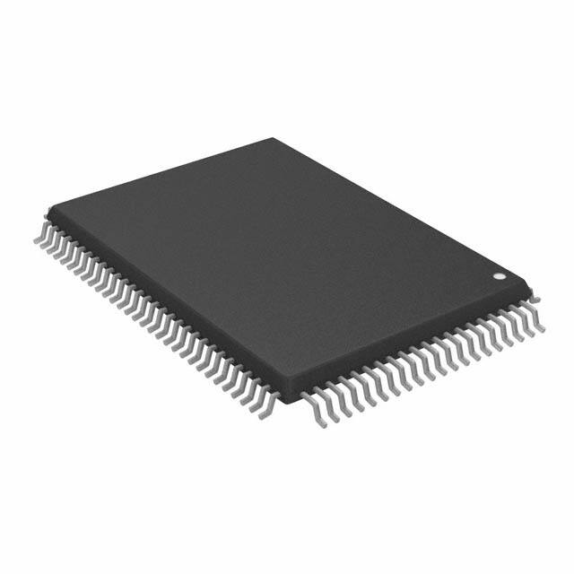
100-Lead MQFP
66/Tray
-G denotes a lead (Pb)-free / RoHS compliant package
Absolute Maximum Ratings
Parameter
Value
VPP, High voltage supply
275V
V+, Low voltage positive supply
7.0V
V-, Low voltage negative supply
-7.0V
HVOUT, Output voltage
0V to 275V
VIN, Analog input signal
0V to 5.0V
Storage temperature range
100
1
(top view)
Product Marking
Top Marking
-65°C to 150°C
Maximum junction temperature
100-Lead MQFP
H V 254FG
LLLLLLLLLL
YYWW
CCCCCCCC AAA
150°C
Absolute Maximum Ratings are those values beyond which damage to the
device may occur. Functional operation under these conditions is not implied.
Continuous operation of the device at the absolute rating level may affect
device reliability. All voltages are referenced to device ground.
YY = Year Sealed
WW = Week Sealed
L = Lot Number
C = Country of Origin
A = Assembler ID
= “Green” Packaging
Package may or may not include the following marks: Si or
100-Lead MQFP
Typical Thermal Resistance
Package
θja
100-Lead MQFP
39OC/W
Operating Conditions
Sym
Parameter
Min
Typ
Max
Units
Conditions
VPP
High voltage positive supply
50
-
275
V
---
V+
Low voltage positive supply
4.75
5.00
5.25
V
---
V-
Low voltage negative supply
-4.75
-5.00
-5.25
V
---
IPP
VPP supply current
1.0
-
2.5
mA
VPP = 275V. All inputs set at 140mV.
Typically 45µA per channel.
I+
V+ supply current
-
-
1.0
mA
V+ = 5.25V
I-
V- supply current
-
-
-3.0
mA
V- = -5.25V
TA
Ambient temperature range
-10
-
70
°C
---
TJ
Operating temperature range
-10
-
125
°C
---
Doc.# DSFP-HV254
C070813
2
Supertex inc.
www.supertex.com
�HV254
Electrical Characteristics (over operating conditions, unless otherwise specified)
High Voltage Amplifier Output
Sym
Parameter
Min
Typ
Max
Units
Conditions
HVOUT
HVOUT voltage swing
7.0
-
250
V
VPP = 275V, Load = 125MΩ//100pF
VIN
Input voltage range
0.14
-
V+
V
--VPP = 275V, 30mV input offset
HVOS
HVOUT DC offset
-
±1.50
±1.52
V
SR
HVOUT slew rate
3.0
-
-
V/µs
VPP = 275V, load = 125MΩ//100pF
RFB
Feedback impedence
8.0
12
-
MΩ
---
AV
Closed loop gain
47.5
50.0
52.5
V/V
---
HVOUT -3dB channel bandwidth
5.0
-
-
KHz
VPP = 275V
HVOUT capacitive load
0
-
100
pF
---
Stability (max drift)
-
-
500
mV
Measured at HVOUT
Min
Typ
Max
Units
BW
CLOAD
Temperature Diode
Sym
Parameter
Conditions
PIV
Peak inverse voltage
-
-
5.0
V
cathode to anode
VF
Forward diode drop
-
-
0.8
V
IF = 100µA, anode to cathode
IF
Forward diode current
-
-
100
µA
anode to cathode
TC
VF temperature coefficient
-
-2.2
-
mV/°C
anode to cathode
Power Up/Down Sequence
Acceptable Power Up Sequences
The HV254 can be powered up with any of the following
sequences listed below.
1) VPP 2) V- 3) V+ 4) Inputs and Anode
or
1) V- 2) V+ 3) VPP 4) Inputs and Anode
External Diode Protection
The device can be damaged due to improper power up/down
sequence. To prevent damage, please follow the acceptable
power up/down sequences and add two external diodes as
shown in the diagram below. The first diode is a high voltage
diode across VPP and V+ where the anode of the diode is
connected to V+ and the cathode of the diode is connected
to VPP. Any low current high voltage diode such as a
1N4004 will be adequate. The second diode is a schottky
diode across V- and DGND where the anode of the schottky
diode is connected to V- and the cathode is connected to
DGND. Any low current schottky diode such as a 1N5817
will be adequate.
V+
Acceptable Power Down Sequences
The HV254 can be powered down with any of the following
sequences listed below.
1) Inputs and Anode 2) V+ 3) V- 4) VPP
or
1) Inputs and Anode 2) VPP 3) V+ 4) V-
VPP
1N4004 or similar
V-
PGND
1N5817 or similar
Doc.# DSFP-HV254
C070813
3
Supertex inc.
www.supertex.com
�HV254
HV254 Block Diagram
VPP
V+
+
Anode
HVOUT0
-
Cathode
VVIN0
49R
R
V+
VPP
+
VIN1
HVOUT1
V49R
R
V+
VPP
+
VIN31
HVOUT31
PGND
49R
R
V-
Doc.# DSFP-HV254
C070813
4
Supertex inc.
www.supertex.com
�HV254
Pad Configuration (not drawn to scale)
PGND
HVOUT31
VIN31
HVOUT30
VIN30
HVOUT29
VIN29
HVOUT28
VIN28
HVOUT27
VIN27
HVOUT26
VIN26
HVOUT25
VIN25
HVOUT24
VIN24
HVOUT23
VIN23
HVOUT22
VIN22
HVOUT21
VIN21
HVOUT20
VIN20
HVOUT19
VIN19
HVOUT18
VIN18
HVOUT17
VIN17
HVOUT16
VIN16
HVOUT15
VIN15
HVOUT14
VIN14
HVOUT13
VIN13
HVOUT12
VIN12
HVOUT11
VIN11
HVOUT10
VIN10
HVOUT9
VIN9
HVOUT8
VIN8
HVOUT7
VIN7
HVOUT6
VIN6
HVOUT5
VIN5
HVOUT4
VIN4
HVOUT3
VIN3
HVOUT2
VIN2
HVOUT1
VIN1
HVOUT0
Doc.# DSFP-HV254
C070813
5
PGND
V+
V+
Anode
Cathode
V-
V-
VPP
VPP
VIN0
Supertex inc.
www.supertex.com
�HV254
Pad Coordinates
Chip size: 4800μm x 11180μm
Center of die is (0,0)
Pad Name
X (μm)
Y (μm)
Pad Name
X (μm)
Y (μm)
Pad Name
X (μm)
Y (μm)
HVOUT31
-1447.5
5244.0
HVOUT5
-1447.5
-3011.0
VIN11
2156.5
-1271.0
HVOUT30
-1447.5
4926.5
HVOUT4
-1447.5
-3328.5
VIN12
2156.5
-957.0
HVOUT29
-1447.5
4609.0
HVOUT3
-1447.5
-3646.0
VIN13
2156.5
-643.0
HVOUT28
-1447.5
4291.5
HVOUT2
-1447.5
-3963.5
VIN14
2156.5
-329.0
HVOUT27
-1447.5
3974.0
HVOUT1
-1447.5
-4281.0
VIN15
2156.5
-15.0
HVOUT26
-1447.5
3656.5
HVOUT0
-1447.5
-4598.5
VIN16
2156.5
299.0
HVOUT25
-1447.5
3339.0
VPP
-2057.0
-4985.0
VIN17
2156.5
613.0
HVOUT24
-1447.5
3021.5
VPP
-1897.0
-4985.0
VIN18
2156.5
927.0
HVOUT23
-1447.5
2704.0
V-
1030.5
-5018.0
VIN19
2156.5
1241.0
HVOUT22
-1447.5
2386.5
V-
1190.5
-5018.0
VIN20
2156.5
1555.0
HVOUT21
-1447.5
2069.0
ANODE
1350.5
-5018.0
VIN21
2156.5
1869.0
HVOUT20
-1447.5
1751.5
CATHODE
1550.5
-5018.0
VIN22
2156.5
2183.0
HVOUT19
-1447.5
1434.0
V+
1710.5
-5018.0
VIN23
2156.5
2497.0
HVOUT18
-1447.5
1116.5
V+
1870.5
-5018.0
VIN24
2156.5
2811.0
HVOUT17
-1447.5
799.0
PGND
2034.5
-5018.0
VIN25
2156.5
3125.0
HVOUT16
-1447.5
481.5
VIN0
2156.5
-4725.0
VIN26
2156.5
3439.0
HVOUT15
-1447.5
164.0
VIN1
2156.5
-4411.0
VIN27
2156.5
3753.0
HVOUT14
-1447.5
-153.5
VIN2
2156.5
-4097.0
VIN28
2156.5
4067.0
HVOUT13
-1447.5
-471.0
VIN3
2156.5
-3783.0
VIN29
2156.5
4381.0
HVOUT12
-1447.5
-788.5
VIN4
2156.5
-3469.0
VIN30
2156.5
4695.0
HVOUT11
-1447.5
-1106.0
VIN5
2156.5
-3155.0
VIN31
2156.5
5009.0
HVOUT10
-1447.5
-1423.5
VIN6
2156.5
-2841.0
PGND
2156.5
5315.5
HVOUT9
-1447.5
-1741.0
VIN7
2156.5
-2527.0
HVOUT8
-1447.5
-2058.5
VIN8
2156.5
-2213.0
HVOUT7
-1447.5
-2376.0
VIN9
2156.5
-1899.0
HVOUT6
-1447.5
-2693.5
VIN10
2156.5
-1585.0
Notes:
1.
2.
3.
4.
The two PGND pads are not electrically connected.
The two VPP pads, V+ pads, and V- pads are electrically connected.
Backside potential is VPP. Leave floating or connect to VPP.
Anode and Cathode are connected to the P and N terminals (respectively) of a silicon diode which can be used to measure temperature.
Doc.# DSFP-HV254
C070813
6
Supertex inc.
www.supertex.com
�HV254
Pin Description
Pin #
Function
1
HVOUT29
2
HVOUT28
3
HVOUT27
4
HVOUT26
5
HVOUT25
6
HVOUT24
7
HVOUT23
8
HVOUT22
9
HVOUT21
10
HVOUT20
11
HVOUT19
12
HVOUT18
13
HVOUT17
14
HVOUT16
15
HVOUT15
16
HVOUT14
17
HVOUT13
18
HVOUT12
19
HVOUT11
20
HVOUT10
21
HVOUT09
22
HVOUT08
23
HVOUT07
24
HVOUT06
25
HVOUT05
26
HVOUT04
27
HVOUT03
28
HVOUT02
29
HVOUT01
30
HVOUT0
Description
Amplifier outputs.
31
32
33
NC
No connect.
34
35
Doc.# DSFP-HV254
C070813
7
Supertex inc.
www.supertex.com
�HV254
Pin Description (cont.)
Pin #
36
Function
Description
VPP
High voltage positive supply.
38
NC
No connect.
39
IBIAS
40
NC
No connect.
V-
Low voltage negative supply.
37
41
42
43
ANODE
44
CATHODE
45
For internal testing only. Leave floating.
Anode side of of a low voltage silicon diode that can be used to monitor die
temperature.
Cathode side of of a low voltage silicon diode that can be used to monitor die
temperature.
V+
Low voltage positive supply.
47
NC
No connect.
48
PGND
49
VIN0
50
VIN1
51
VIN2
52
VIN3
53
VIN4
54
VIN5
55
VIN6
56
VIN7
57
VIN8
58
VIN9
59
VIN10
60
VIN11
61
VIN12
62
VIN13
63
VIN14
64
VIN15
65
VIN16
66
VIN17
67
VIN18
46
Doc.# DSFP-HV254
C070813
Power ground. Two PGND pads. Need to be externally connected.
Amplifier inputs.
8
Supertex inc.
www.supertex.com
�HV254
Pin Description (cont.)
Pin #
Function
68
VIN19
69
VIN20
70
VIN21
71
VIN22
72
VIN23
73
VIN24
74
VIN25
75
VIN26
76
VIN27
77
VIN28
78
VIN29
79
VIN30
80
VIN31
81
PGND
Description
Amplifier inputs.
Power ground. Two PGND pads. Need to be externally connected.
82
83
84
85
86
87
88
89
90
NC
No connect.
91
92
93
94
95
96
97
98
99
HVOUT31
100
HVOUT30
Doc.# DSFP-HV254
C070813
Amplifier outputs.
9
Supertex inc.
www.supertex.com
�HV254
100-Lead MQFP Package Outline (FG)
20.00x14.00mm body, 3.15mm height (max), 0.65mm pitch, 3.20mm footprint
D
D1
E
E1
Note 1
(Index Area
E1/4 x D1/4)
100
1
e
b
Top View
θ1
View B
A A2
L2 Gauge
Plane
Seating
Plane
A1
L
L1
Side View
Seating
Plane
θ
View B
Note:
1. A Pin 1 identifier must be located in the index area indicated. The Pin 1 identifier can be: a molded mark/identifier; an embedded metal marker; or
a printed indicator.
Symbol
A
MIN
Dimension
NOM
(mm)
MAX
A1
A2
b
2.50* 0.00 2.50 0.22
3.15
-
2.70
-
0.25 2.90 0.40
D
D1
E
E1
22.95*
19.80*
16.95*
13.80*
23.20
20.00
17.20
14.00
23.45*
20.20*
17.45*
14.20*
e
L
0.73
L1
L2
0.65
1.60 0.25
0.88
BSC
REF BSC
1.03
θ
θ1
0O
5O
-
-
7
16O
O
JEDEC Registration MS-022, Variation GC-2, Issue B, Dec. 1996.
* This dimension is not specified in the JEDEC drawing.
Drawings are not to scale.
Supertex Doc. #: DSPD-100MQFPFG, Version F041309.
(The package drawing(s) in this data sheet may not reflect the most current specifications. For the latest package outline
information go to http://www.supertex.com/packaging.html.)
Supertex inc. does not recommend the use of its products in life support applications, and will not knowingly sell them for use in such applications unless it receives
an adequate “product liability indemnification insurance agreement.” Supertex inc. does not assume responsibility for use of devices described, and limits its liability
to the replacement of the devices determined defective due to workmanship. No responsibility is assumed for possible omissions and inaccuracies. Circuitry and
specifications are subject to change without notice. For the latest product specifications refer to the Supertex inc. (website: http//www.supertex.com)
Supertex inc.
©2013 Supertex inc. All rights reserved. Unauthorized use or reproduction is prohibited.
Doc.# DSFP-HV254
C070813
10
1235 Bordeaux Drive, Sunnyvale, CA 94089
Tel: 408-222-8888
www.supertex.com
�
很抱歉,暂时无法提供与“HV254FG-G”相匹配的价格&库存,您可以联系我们找货
免费人工找货