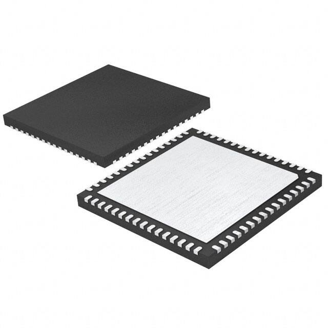
HV2621/HV2721/HV2722
300V, Low-Charge Injection, 16-Channel,
High-Voltage Analog Switch
Features
General Description
•
•
•
•
•
•
•
•
•
•
•
The HV2621/HV2721/HV2722 devices are 300V,
low-charge injection, 16-channel, high-voltage analog
switches. These devices are designed for use in
applications
requiring
high-voltage
switching
controlled by low-voltage control signals, such as
medical ultrasound imaging, piezoelectric transducer
drivers. HV2621/HV2721 are almost identical to
HV2601/2701 but have larger signal range. If the
VPP/VNN = ±150V, HV2621/HV2721/HV2722 can pass
the analog signal up to ±135V.
The HV2721 has integrated bleed resistors on both
sides of the switches. HV2722 has integrated bleed
resistors on one side, SWxA only. HV2621 has no
bleed resistors. The bleed resistor eliminates voltage
build-up on capacitive loads such as piezoelectric
transducers.
Input data are shifted into a 16-bit shift register that
can then be retained in a 16-bit latch. To change all the
switch state at the same time, the latch enable bar
should be left high until all bits are clocked in. The
input data are clocked in at the rising edge of the
clock. After all bits are clocked in to the shift register, a
negative pulse of the latch enable bar changes all the
switch ON/OFF states defined by input data at the
same time. Using the HVCMOS technology, these
devices combine 300V high-voltage bilateral DMOS
switches and low-power CMOS logic to provide
efficient control of high-voltage analog signals.
These devices are suitable for various combinations of
high-voltage supplies, e.g., VPP/VNN: +60V/-240V,
+150V/-150V, and +260V/-40V.
300V,16-Channel High-Voltage Analog Switch
3.3V or 5.0V CMOS Input Logic Level
33 MHz Data Shift Clock Frequency
Very Low Quiescent Current (10 µA)
Low Parasitic Capacitance
DC to 50 MHz Analog Small-Signal Frequency
-60 dB Typical Off Isolation at 5.0 MHz
Excellent Noise Immunity
Cascadable Serial Data Register with Latches
Flexible Operating Supply Voltage
Integrated Bleed Resistors on the Outputs (both
sides for HV2721, one side only for HV2722)
Applications
• Medical Ultrasound Imaging
• Nondestructive Testing (NDT) Metal Flaw
Detection
• Multi-Layer Printed Circuit Board (PCB) Tester
• Piezoelectric Transducer Drivers
• Inkjet Printer Head
• Optical MEMS Module
Package Types
64
HV2621/HV2721/HV2722
9x9x1.0mm QFN
(TOP VIEW)
1
2019 Microchip Technology Inc.
DS20006082A-page 1
�HV2621/HV2721/HV2722
Block Diagram
Latches
CLK
Level
Shifter
Output
Switches
Bleed
Resistors
D
LE
CLR
SW0A
D
LE
CLR
SW1A
D
LE
CLR
SW2A
D
LE
CLR
SW14A
D
LE
CLR
SW15A
SW0B
SW1B
SW2B
16-Bit
Shift
Register
DIN
DOUT
VDD
GND
LE CLR
SW14B
SW15B
VNN VPP
RGND
HV2721 has bleed resistors at SWxA and SWxB
HV2722 has bleed resistors at SWxA only
DS20006082A-page 2
2019 Microchip Technology Inc.
�HV2621/HV2721/HV2722
1.0
ELECTRICAL CHARACTERISTICS
Absolute Maximum Ratings †
Logic Supply Voltage (VDD).......................................................................................................................... -0.5V to 6.5V
Differential Supply Voltage (VPP-VNN).......................................................................................................................330V
Positive Supply Voltage (VPP) .............................................................................................................-0.5V to VNN+300V
Negative Supply Voltage (VNN) ................................................................................................................. -300V to +0.5V
Logic Input Voltage (VIN).....................................................................................................................-0.5V to VDD +0.3V
Analog Signal Range (VSIG)............................................................................................................................ VNN to VPP
Peak Analog Signal Current/Channel (IPK) ...................................................................................................................3A
† Notice: Stresses above those listed under “Maximum Ratings” may cause permanent damage to the device. This is
a stress rating only and functional operation of the device at those or any other conditions above those indicated in the
operational sections of this specification is not intended. Exposure to maximum rating conditions for extended periods
may affect device reliability.
RECOMMENDED OPERATING CONDITIONS (NOTES 1, 2, 3)
Parameter
Sym.
Min.
Typ.
Max.
Units
VDD
3
—
5.5
V
VPP-VNN
60
—
300
V
Positive Supply Voltage
VPP
60
—
260
V
Negative Supply Voltage
VNN
-240
—
0
V
High-Level Input Voltage
VIH
0.9VDD
—
VDD
V
Logic Supply Voltage
Differential Supply Voltage
Low-Level Input Voltage
Analog Signal Voltage Peak-to-Peak
Note 1:
2:
3:
VIL
0
—
0.1VDD
V
VSIG
VNN+15
—
VPP-15
V
Conditions
Recommended power up sequence is VDD, VPP and VNN. Power down is in reverse order.
VSIG must be VNN ≤ VSIG ≤ VPP or floating during power up/down transition.
Rise and fall times of power supplies, VDD, VPP and VNN should be greater than 1.0 ms.
DC ELECTRICAL CHARACTERISTICS
Unless otherwise specified, VPP = +150V, VNN = -150V, VDD = 5.0V, TA = 25°C. Boldface specifications apply over
the full operating temperature range.
Parameter
Small Signal Switch On-Resistance
Sym.
RONS
Min.
Typ.
Max.
Units
Conditions/Comments
—
26
48
Ω
ISIG = 5 mA
—
22
32
Ω
ISIG = 150 mA
—
22
30
Ω
ISIG = 5 mA
—
18
27
Ω
ISIG = 150 mA
—
20
30
Ω
ISIG = 5 mA
—
16
27
Ω
ISIG = 150 mA
VPP = +60V,
VNN = -240V
VPP = +150V,
VNN = -150V
VPP = +260V,
VNN = -40V
Small Signal Switch On-Resistance
Matching
∆RONS
—
5
20
%
ISIG = 5 mA, VPP = +150V,
VNN = -150V
Large Signal Switch On-Resistance
RONL
—
17
—
Ω
VSIG = VPP-15V, ISIG =1A
Value of Output Bleed Resistor
(HV2721/HV2722 Only)
RINT
30
50
70
kΩ
Output switch to RGND,
IRINT = 0.5 mA
Switch Off Leakage per Switch
ISOL
—
1
15
μA
VSIG = VPP-15V, VNN+15V.
See Figure 3-1
—
1
10
mV
RLOAD = 35 kΩ (HV2621), 70 kΩ
(HV2722), No load (HV2721), see
Figure 3-2
DC Offset Switch Off
DC Offset Switch On
2019 Microchip Technology Inc.
VOS
—
1
10
DS20006082A-page 3
�HV2621/HV2721/HV2722
DC ELECTRICAL CHARACTERISTICS (CONTINUED)
Unless otherwise specified, VPP = +150V, VNN = -150V, VDD = 5.0V, TA = 25°C. Boldface specifications apply over
the full operating temperature range.
Parameter
Sym.
Min.
Typ.
Max.
Units
Quiescent VPP Supply Current
IPPQ
—
10
50
μA
Quiescent VNN Supply Current
INNQ
—
10
50
μA
Quiescent VPP Supply Current
IPPQ
—
10
50
μA
Quiescent VNN Supply Current
INNQ
—
10
50
μA
Switch Output Peak Current
ISW
2.0
3.0
—
A
Output Switching Frequency
fSW
—
—
50
kHz
Duty cycle = 50% (Note 1)
—
—
3
mA
VPP = +60V,
VNN = -240V
—
—
4
mA
VPP = +150V,
VNN = -150V
—
—
—
6
mA
VPP = +260V,
VNN = -40V
—
—
3
mA
VPP = +60V,
VNN = -240V
—
—
4
mA
VPP = +150V,
VNN = -150V
—
—
—
6
mA
VPP = +260V,
VNN = -40V
IDD
—
—
4
mA
fCLK = 5 MHz, fDIN= 2.5 MHz
IDDQ
—
—
10
μA
All logic inputs are static
Average VPP Supply Current
Average VNN Supply Current
Average VDD Supply Current
Quiescent VDD Supply Current
IPP
INN
Conditions/Comments
All switches off
All switches on, ISW = 5.0 mA
VSIG duty cycle