HV9150
High-Voltage Output Hysteretic-Mode Step-Up DC/DC Controller
Features
General Description
• 6V to 500V Wide Output Voltage Range
• 2.7V Low Input Voltage
• 5W Maximum Output Power with External
MOSFET Driver
• Built-in Charge Pump Converter for the Gate
Driver
• Programmable Switching Frequency from 40 kHz
to 400 kHz
• Four Programmable Duty Cycles from 50% to
87.5%
• FB Return Ground Switch for Power-Saving
Applications
• Built-In Delay Timer for Internal Protection
• Non-Isolated DC/DC Converter
The HV9150 is a high output voltage Hysteretic mode
step-up DC/DC controller that has a built-in charge
pump converter and a linear regulator for a wide range
of input voltage. The Charge Pump Converter mode is
ideal for battery-powered applications. The internal
converter can provide a minimum of 5V gate driver
output voltage (at VIN = 2.7V) to the external N-channel
MOSFET. The range of 2.7V to 4.5V input supply
voltage is ideal for battery-powered applications, such
as portable electronic equipment. The internal linear
regulator is selected when a higher supply voltage rail
is available in the system.
Applications
In addition, a built-in timer is available to protect the
internal circuit and help dissipate the energy from the
external high-voltage storage capacitor. This device is
designed for systems requiring high-voltage and
low-current applications such as MEMS devices.
A feedback return ground path switch is also integrated
into the device to minimize the quiescent current during
the controller shutdown. This feature provides power
savings for energy-critical applications.
• Portable Electronic Equipment
• MEMS
• Printers
Package Type
CCP2+
CCP2-
CCP1+
CCP1-
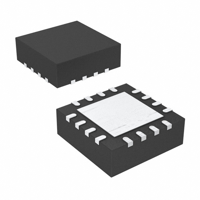
16-lead QFN
(Top View)
16
VLL
1
VDD
GND
GATE
EN
FB_RTN
CT
EXT_REF
FREQ_ADJ
FB
VCONTROL
CP_EN
Pads are at the bottom of the package. Center heat slug is at ground potential. See Table 3-1 for pin information.
2017-2019 Microchip Technology Inc.
DS20005689B-page 1
�HV9150
Functional Block Diagram
VDD
CCP1+/-
CCP2+/-
VLL
CP
Mode
3x Charge Pump
Converter
LDO
Mode
VLL
VDD
LDO
VLL
CP_EN
VDD
VCONTROL
(Duty Cycle Adj)
GATE
OSC
VLL
FREQ_ADJ
VLL
VREF
-
+
Hysteretic Mode
Controller
EXT_REF
FB
FP_RTN
EN
Delay
CT
DS20005689B-page 2
GND
2017-2019 Microchip Technology Inc.
�HV9150
Typical Application Circuits
VDD
0.22μF
CCP1± CCP2±
0.22μF 0.22μF
VIN
2.7 - 4.5V
1.0μF
VLL
CP
Mode
L
LDO
Mode
VDD
3x Charge Pump
Converter
LDO
CP_EN
VLL
VOUT
6.0 - 500V
VDD
VCONTROL
GATE
OSC
VLL
VLL
FREQ_ADJ
VREF
- +
RFREQ
EXT_REF
FB
R2
FB_RTN
0V/3.3V
R1
EN
Delay
CT
GND
Charge Pump (CP) Mode
VDD
CCP1± CCP2±
CP
Mode
3x Charge Pump
Converter
VIN
5.0 - 12V
1.0μF
VLL
L
LDO
Mode
VDD
LDO
CP_EN
VLL
VOUT
15 - 500V
VDD
GATE
VCONTROL
OSC
VLL
VLL
FREQ_ADJ
VREF
- +
RFREQ
EXT_REF
FB
R2
FB_RTN
0V/3.3V
EN
R1
Delay
CT
GND
Linear Regulator (LDO) Mode
2017-2019 Microchip Technology Inc.
DS20005689B-page 3
�HV9150
1.0
ELECTRICAL CHARACTERISTICS
Absolute Maximum Ratings†
Input Voltage Supply, VLL ........................................................................................................................... –0.5V to +5V
Charge Pump Output Voltage, VDD ....................................................................................................... –0.5V to +13.6V
Logic Input Levels ............................................................................................................................. –0.5V to VLL +0.5V
Operating Ambient Temperature, TA ................................................................................................... –25°C to +125°C
Storage Temperature, TS...................................................................................................................... –65°C to +150°C
Continuous Power Dissipation (On a 3 x 4-inch FR4 PCB at TA= 25°C):
16-lead QFN .......................................................................................................................................... 3000 mW
† Notice: Stresses above those listed under “Absolute Maximum Ratings” may cause permanent damage to the
device. This is a stress rating only, and functional operation of the device at those or any other conditions above those
indicated in the operational sections of this specification is not intended. Exposure to maximum rating conditions for
extended periods may affect device reliability.
RECOMMENDED OPERATING CONDITIONS
Parameter
Sym.
Min.
Typ.
Max.
Unit
Input Voltage (CP Mode)
VLL
2.7
—
4.5
V
High-level Input Voltage
VIH
0.8 VLL
—
VLL
V
Low-level Input Voltage
VIL
0
—
0.2 VLL
V
Conditions
DC ELECTRICAL CHARACTERISTICS
Electrical Specifications: Over recommended operating supply voltages and temperatures; unless otherwise noted,
TJ = 25°C.
Parameter
Sym.
Min.
Typ.
Max.
Unit
ILLQ(off)
—
—
2
μA
—
—
1.5
—
—
4
—
—
1
—
—
2.5
Conditions
POWER SUPPLY
Quiescent VLL Supply Current
(EN = ‘0’)
VLL Supply Current
(EN = ‘1’)
GATE = NC
GATE = 300 pF
ILL(on)
mA
fOSC = 100 kHz, VLL = 4.5V
mA
fOSC = 100 kHz, VDD = 12.6V
VDD Supply Current GATE = NC
(EN = ‘1’)
GATE = 300 pF
IDD(on)
Quiescent VDD Supply Current
(EN = ‘0’)
IDDQ(off)
—
—
2
μA
High-level Logic Input Current
IIH
—
—
1
μA
VIH = VLL
Low-level Logic Input Current
IIL
—
—
–1
μA
VIL = 0V
10.2
—
12.3
Gate Driver Output
Voltage
VLL = 4.5V
GATE = NC
VLL = 2.7V
GATE = NC
Linear Regulator Output Voltage
DS20005689B-page 4
GATE
VLL(LDO)
V
5
—
6.9
3
—
3.6
V
2017-2019 Microchip Technology Inc.
�HV9150
AC ELECTRICAL CHARACTERISTICS
Electrical Specifications: Over recommended operating supply voltages and temperatures; unless otherwise noted
TJ = 25°C.
Parameter
Sym.
Min.
Typ.
Max.
Unit
1.22
1.25
1.28
1.2
1.25
1.3
—
—
1
μA
0
—
VLL–1.4
V
0
—
0.12
V
0.5
—
VLL–1.4
V
—
—
500
Ω
—
—
13.5
V
Conditions
FEEDBACK (FB)
Internal Feedback Reference
Voltage
Accuracy
VREF
Range
Input Bias Current
IBIAS
Range
External
Reference
Voltage
Trigger INT
Reference
EXT_REF
Trigger EXT
Reference
On-resistance, RDS
Breakdown Voltage, BV
FB_RTN
V
TA = –25 to 85°C
EXT_REF is selected.
During EN positive triggering
IO= 2 mA
GATE DRIVER OUTPUT (GATE)
Rise Time
tr
—
—
36
ns
Fall Time
tf
—
—
12
ns
—
—
45
—
—
30
—
—
15
—
—
12
—
½ fOSC
—
Pull-up
Resistance
VDD = 5V
Pull-down
Resistance
VDD = 5V
RUP
VDD = 12V
RDOWN
VDD = 12V
Oscillator Frequency
fGATE
Ω
Ω
CL = 300 pF, VDD = 12V
IO = 20 mA
IO = 50 mA
IO = 20 mA
IO = 50 mA
kHz
CHARGE PUMP CONVERTER
Charge Pump Output Voltage
Oscillator
Frequency
VDD
Accuracy
fOSC
Range
Oscillator Frequency Tolerance
∆f
Accuracy
Duty Cycle
12.6
170
195
220
40
—
400
V
kHz
RFREQ = 270 kΩ, VLL= 3.3V
Over RFREQ range
—
15
—
%
50 kHz ≤ fOSC ≤ 250 kHz
86
87.5
90
%
RFREQ = 270 kΩ
—
0
—
%
0 < VCNTL ≤ 0.18 VLL
50
—
%
0.22 VLL < VCNTL ≤ 0.38 VLL
—
62.5
—
%
0.42 VLL < VCNTL ≤ 0.58 VLL
—
75
—
%
0.62 VLL < VCNTL ≤ 0.78 VLL
—
87.5
—
%
0.82 VLL < VCNTL ≤ VLL
VCONTROL
0
—
VLL
V
See Table 4-2.
RFREQ
120k
—
1.2M
Ω
—
—
20
—
—
20
Frequency Adjustment Resistor
Maximum Charge
Pump Output
Resistance
3 VLL–1.8
—
DC
Range
Duty Cycle Adjustment
5
2.7V ≤ VLL ≤ 4.5V
CCP1 = 220 nF
CCP2 = 220 nF
CCP3 = 220 nF
Pull-up
Pull-down
2017-2019 Microchip Technology Inc.
RCP
Ω
VLL = 2.7V, IO = 10 mA
DS20005689B-page 5
�HV9150
AC ELECTRICAL CHARACTERISTICS (CONTINUED)
Electrical Specifications: Over recommended operating supply voltages and temperatures; unless otherwise noted
TJ = 25°C.
Parameter
Sym.
Output Ripple at VDD
Min.
Typ.
Max.
Unit
Conditions
VRIPPLE
—
—
100
mV
2.7V ≤ VLL ≤ 4.5V
fOSC = 200 kHz
CCP1 = 220 nF
CCP2 = 220 nF
CCP3 = 220 nF
CGATE = 300 pF
BW = 20 MHz
tDELAY
—
240
—
ms
CT = 1 μF
DELAY TIMER
Shutdown Delay Timer
TEMPERATURE SPECIFICATIONS
Parameter
Sym.
Min.
Typ.
Max.
Unit
Operating Ambient Temperature
TA
–25
—
+125
°C
Storage Temperature
TS
–65
—
+150
°C
—
33
—
°C/W
Conditions
TEMPERATURE RANGE
PACKAGE THERMAL RESISTANCE
JA
16-lead QFN
100
87.5% Duty Cycle
87.5% Duty Cycle
90
82%
80
78%
Percentage of VLL
60
62%
58%
62.5% Duty Cycle
62.5% Duty Cycle
50
40
75% Duty Cycle
75% Duty Cycle
70
42%
38%
50% Duty Cycle
50% Duty Cycle
30
22%
20
10
0
FIGURE 1-1:
DS20005689B-page 6
18%
0% Duty Cycle
0% Duty Cycle
VCONTROL from Max to Min
VCONTROL from Min to Max
Duty Cycle Selection Hysteresis at VCONTROL Pin at 25°C.
2017-2019 Microchip Technology Inc.
�HV9150
Timing Waveforms
XQWV"*GZVaTGH+
XQWV"*KPVaTGH+
XQWV
2X
XKJ
GP
XKN
Initial power up
FIGURE 1-2:
Enabling to use the External Voltage Reference.
XQWV
2X
tDELAY
HDaTVP
2X
XKJ
GP
FIGURE 1-3:
XKN
Delay Time at FB_RTN.
VIN = 4.5V
VIN = 2.7V
FIGURE 1-4:
VCP Noise.
2017-2019 Microchip Technology Inc.
DS20005689B-page 7
�HV9150
2.0
TYPICAL PERFORMANCE CURVES
Note:
The graphs and tables provided following this note are a statistical summary based on a limited number of
samples and are provided for informational purposes only. The performance characteristics listed herein
are not tested or guaranteed. In some graphs or tables, the data presented may be outside the specified
operating range (e.g. outside specified power supply range) and therefore outside the warranted range.
35
12.0
Charge Pump Output Voltage VDD (V)
30
Rise time tr, VDD = 5V
(LDO mode)
25
11.0
CL = 100 pF
CL = 220 pF
CL = 330 pF
10.0
Rise time tr, VDD = 11V
(CP mode)
Time (ns)
20
15
Fall time tf, VDD = 5V
(LDO mode)
10
Fall time tf, VDD = 11V
(CP mode)
5
0
9.0
8.0
7.0
6.0
0
50
100
150
200
250
300
350
2.5
3.0
3.5
Load Capacitance (pF)
4.5
5.0
FIGURE 2-4:
Charge Pump Output
Voltage vs. Input Voltage at 25°C.
FIGURE 2-1:
Gate Driver Rise Time (tr)
and Fall Time (tf) vs. Load Capacitance at
25°C.
(VIN = 3.3V at 25OC)
1000
4.0
Input Voltage VLL (V)
(fGATE = 100 kHz, CCP1 = CCP2 = 0.22 µF, CVDD = 1.0 µF)
12
VLL = 4.5V
Output Voltage VDD (V)
Frequency (kHz)
11
100
10
9
VLL = 3.6V
8
VLL = 3.3V
7
6
10
10
100
1000
5
RFREQ (kΩ)
0
50
100
150
200
250
300
350
Load Capacitance (pF)
fGATE vs. RFREQ.
FIGURE 2-2:
VLL = 2.7V
FIGURE 2-5:
Charge Pump Output
Voltage vs. Load Capacitance at 25°C.
(Gate output load capacitance = 330 pF, RFREQ = 255 kΩ @ 25OC)
100
101
CP mode
Frequency (kHz)
Capacitance (µF)
100
10
1
99
LDO mode
98
97
96
0.1
10
100
1000
Delay (ms)
FIGURE 2-3:
CT Capacitor Value vs.
Delay Time at 25°C.
DS20005689B-page 8
10000
2
3
4
5
6
7
8
9
10
11
12
13
14
VLL Input Voltage (V)
FIGURE 2-6:
Gate Driver Switching
Frequency vs. VLL Input Voltage.
2017-2019 Microchip Technology Inc.
�HV9150
3.0
PIN DESCRIPTION
The details of the pins of HV9150 16-lead QFN are
listed in Table 3-1. Refer to Package Type for the pin
locations.
TABLE 3-1:
PIN FUNCTION TABLE
Pin Number
Pin Name
1
VLL
Input supply voltage
2
GND
Ground connection
3
EN
4
CP_EN
5
VCONTROL
Duty cycle adjustment voltage control input
6
FREQ_ADJ
Frequency adjustment
7
EXT_REF
8
CT
Timing capacitor
9
FB
Feedback input voltage
10
FB_RTN
11
GATE
Gate control output
12
VDD
Charge pump output voltage
13
CCP2+
Charge pump storage capacitor #2 plus terminal
14
CCP2–
Charge pump storage capacitor #2 minus terminal
15
CCP1+
Charge pump storage capacitor #1 plus terminal
16
CCP1–
Charge pump storage capacitor #1 minus terminal
Center Pad
Description
Enable
Charge pump/LDO enable input
External reference voltage input
Feedback return
Substrate connection (at ground potential)
2017-2019 Microchip Technology Inc.
DS20005689B-page 9
�HV9150
4.0
FUNCTIONAL DESCRIPTION
Follow the steps in Table 4-1 to power up and power
down the HV9150.
TABLE 4-1:
POWER-UP AND POWER-DOWN SEQUENCE
Power-up
Step
1
2
3
Power-down
Description
Step
Connect ground.
Apply VIN.
Set all inputs to a known state.
4.1
1
2
3
Hysteretic Mode Controller
4.2
A Hysteretic mode controller consists of an oscillator, a
voltage reference, a comparator and a driver. Both the
internal oscillator and the duty cycle of the gate driver
are running at a fixed rate.
As this device is designed for a step-up conversion, a
pulse train is used to control the switch of a classical
switching boost converter. The pulse train is gated by
the output of the comparator, which compares the
feedback of the output voltage with the voltage
reference.
If the output voltage reaches the target voltage, the
comparator will turn off the pulse train. When the output
voltage drops below the target voltage, the comparator
will pass the pulse train to the switch and start the
inductor charging cycle. The advantage of this
Hysteretic mode controller is its stability and simple
operation. The diagram in Figure 4-1 shows a
Hysteretic Mode controller and a classical boost
converter.
XKP
XQWV
J{uvgtgvke"Oqfg
Eqpvtqnngt
FIGURE 4-1:
A Hysteretic Mode
Controller and a Classical Boost Converter.
DS20005689B-page 10
Description
Remove all inputs.
Remove VIN.
Disconnect ground.
Internal Oscillator
This device has an internal oscillator which generates
the reference clock for the Hysteretic mode controller.
The controller is running at half of the frequency of the
internal oscillator. This oscillator is powered by the VLL
power supply pin. The frequency of the oscillator is set
by the external resistor RFREQ, and this frequency is
inversely proportional to the value of RFREQ. Its
characteristic is shown in Figure 2-2, fGATE vs. RFREQ
diagram, where fGATE = 1/2 fOSC. See Equation 4-1.
EQUATION 4-1:
1
f OSC = ----------------------------------4 R FREQ C
Where: C = 4.75 pF
4.3
Voltage Reference (VREF)
The voltage reference is used by the comparator to
compare it with the feedback voltage and the boost
converter output. This device provides the options of
using either its internal voltage reference or an external
voltage reference.
The internal voltage reference provides a stable 1.25V
with a tolerance of ±2.5%. With the use of ±1%
tolerance feedback resistors, the output can be
achieved with a tolerance of ±4.5%. In order to use the
internal voltage reference, the EXT_REF pin must be
connected to ground.
If the output voltage of the boost converter is required
to have high precision and tight tolerance, the external
voltage reference can be used to achieve that purpose.
The external reference voltage must be between 0.5V
and VLL–1.4V and connected to the EXT_REF pin. A
single low-to-high transition must be presented at the
EN pin to trigger the device to select an external
voltage reference. If no enable control signal is
available in the application, this signal can be easily
mimicked by a simple RC circuit. See Figure 4-2.
2017-2019 Microchip Technology Inc.
�HV9150
4.6
VIN
EXT_REF
GND
EXT_REF
Internal
FIGURE 4-2:
Reference.
4.4
Voltage
Reference
GND
External
Voltage Connection
Gate Driver (Gate)
The MOSFET gate driver of this controller is especially
designed to drive the gate of the external MOSFET up
to 12V. A high pulse voltage will help minimize the
on-resistance of the external MOSFET transistor. A
lower on-resistance improves the overall efficiency and
heat dissipation.
This gate driver is powered by the supply voltage VDD
which can be generated by either the internal charge
pump converter (CP mode) or the external power
supply (LDO mode), depending on the available
voltage supply rail of the application. See Typical
Application Circuits.
4.5
Charge Pump Converter
(CP Mode)
A 3X charge pump converter is integrated into this
device to provide a 5V to 12V rail for the gate driver.
(See Figure 4-3.) It can be activated by setting CP_EN
to ground. A 3.3V supply is more common and easily
available for digital logic systems. However, this
voltage level is less desirable for driving a high-voltage
MOSFET to obtain a lower on-resistance, which
improves efficiency.
To reduce the number of supply rails used in the
system, an internal two-stage charge pump converter
is added, which can boost the 3.3V supply voltage to
8V. Compared to a 3.3V gate driver, an 8V gate driver
output will substantially improve the on-resistance of
the external MOSFET.
The charge pump input can operate with an input
voltage from 2.7V to 4.5V. Its input and output are
connected to the VLL and VDD pins, respectively.
XNN
XFF
Linear Regulator (LDO Mode)
In some applications, efficiency may be a key factor,
and higher voltage rails such as 5V, 6V, 9V or 12V may
be available in the system. The internal charge pump
converter cannot operate with these voltage levels
because of the maximum output voltage limit of the
charge pump converter. At the same time, these
voltage levels are high enough to provide adequate
supply for the gate driver.
Under this circumstance, an internal linear regulator is
used to replace the charge pump converter. This linear
regulator input can accept voltage from 5V to 12V and
generate a 3.3V output to supply the internal circuit.
This linear regulator can be activated by setting CP_EN
to VLL.
In a scenario when the device is operating in LDO
mode and in Shutdown state (EN = ‘0’), the voltage at
VLL is undefined. To wake up the controller device, a
voltage above 2.7V has to be presented at the enable
pin (EN).
4.7
FB Ground Return Switch
(FB_RTN)
Any DC/DC controller requires feedback from the
output to monitor its operation so that it can regulate its
output accordingly. A simple resistor network is used in
conjunction with a feedback ground switch as a
feedback path. The purpose of this feedback ground
switch is to save power consumed by the feedback
resistor network when the controller is disabled. This
function is quite useful for power saving, especially for
battery-operated applications.
4.8
Shutdown Timer and Timing
Capacitor (CT)
A shutdown timer is also integrated into the controller
for safety purposes. When the controller shuts down
from its normal operation, the converter’s initial output
is still at its high level. If the feedback ground return
switch is disabled at the same time, a current path is
created from the output via the feedback resistor and
the internal protection clamping diode at the FB pin.
(See Figure 4-4.) Depending upon the value of the FB
resistor, this momentarily conducting current can be
high enough to damage this clamping diode. To avoid
this potential problem, a timer is added to the disable
function to keep the feedback ground switch to on
position for a short period of time. This on-time duration
is controlled by an external capacitor CT. The larger the
capacitor value is, the longer the on-time is. Its
characteristic is shown in Figure 2-3.
QUE
FIGURE 4-3:
Converter.
A 3X Charge Pump
2017-2019 Microchip Technology Inc.
DS20005689B-page 11
�HV9150
4.10
VOUT
R2
FB
Internal
Protection
Diode
R1
FB_RTN
0V/3.3V
EN
Delay
CT
Duty Cycle Control (VCONTROL)
The input voltage at the VCONTROL pin manages the
duty cycle of the internal oscillator output to the gate
driver. All internal comparators are powered by the VLL
supply and all their input threshold voltages are
referenced to VLL voltage. A voltage divider formed by
the two external resistors shown in Figure 4-6 can be
adjusted accordingly to select the desired duty cycle of
the pulse signal to the gate driver. See Table 4-2.
GND
TABLE 4-2:
FIGURE 4-4:
FB Pin.
4.9
VCONTROL
Internal Protection Diode at
The controller enable pin (EN), serves two main
purposes. The most obvious function is to turn on and
off the controller, and the other function is to act as a
trigger to activate the device to accept external voltage
reference.
For any applications requiring a highly precise voltage
reference, an external voltage reference should be
used. To activate the device to accept the external
voltage reference, a low-to-high transition has to
appear at the EN pin while the voltage at the EXT_REF
pin is above 0.5V.
0.22 VLL to 0.38 VLL
50%
62.5%
0.62 VLL to 0.78 VLL
87.5%
VLL
VLL
VCONTROL
EN
+
-
Duty Cycle 87.5%
+
-
Duty Cycle 75.0%
+
-
Duty Cycle 62.5%
+
-
Duty Cycle 50.0%
GND
Simple RC Circuit for EN
FIGURE 4-6:
DS20005689B-page 12
75%
0.82 VLL to 1 VLL
R
C
0%
0.42 VLL to 0.58 VLL
If the system lacks enable function control, an RC
circuit can be used to mimic this function to allow the
external voltage reference. Refer to Figure 4-5.
FIGURE 4-5:
Pin.
Duty Cycle
0 VLL to 0.18 VLL
Hysteretic Controller Enable
3.3V (min)
DUTY CYCLE SELECTION
Duty Cycle Control Circuit.
2017-2019 Microchip Technology Inc.
�HV9150
4.11
Design Procedure
There are several parameters that a user needs to
consider for the DC/DC converter design. The input
voltage, output voltage and output power requirement
are usually defined at the beginning. The other
parameters that may be included are: operating
frequency, inductor value, duty cycle and the
on-resistance of the MOSFET. There is some degree of
flexibility in deciding the values of these parameters.
The following provides the user a general design
approach:
4.11.1
STEP 1
Since this DC/DC controller device is operating in a
Discontinuous Conduction mode, determine the
inductance and the switching frequency with
Equation 4-2.
EQUATION 4-2:
Given:
D = Duty cycle
R = Load resistance of the high voltage output
Vi = Minimum input voltage
Vo = Output voltage
Unknown:
L = Inductance
fGATE = Driver switching frequency
Where:
2
Vi
4D
V o = ----- 1 + 1 + ----------
2
K
2 L f GATE
K = -------------------------------R
The maximum duty cycle can be computed with
Equation 4-3.
EQUATION 4-3:
V
D MAX = 1 – ------i
Vo
4.11.2
STEP 2
The standard inductor is usually sold in an incremental
inductance value, for example, 10 µH, 22 µH, 33 µH or
47 µH. The user can choose the inductance based on
the size of the inductor, the peak current, the maximum
operating frequency and the DC resistance. After the
value of L is decided, the gate driver switching
frequency can be computed. The required RFREQ
resistance can be found in the fGATE vs. RFREQ
diagram. (See Figure 2-2.) Next, the user may check
the peak current of the inductor with Equation 4-4. The
saturation current of the inductor must be larger than
IPEAK.
EQUATION 4-4:
Vi D
I PEAK = ----------------------L f GATE
4.11.3
STEP 3
The most important factors in determining the
MOSFET are the breakdown voltage, the current
capability, the on-resistance, the minimum VGS
threshold voltage and the input capacitance.
The HV9150 gate driver is designed to drive a
maximum of 300 pF capacitive load. Therefore, the
maximum input capacitance of the external MOSFET
should be less than 300 pF. The minimum breakdown
voltage must be larger than the required DC/DC
converter output voltage. If the breakdown voltage is
too low, the output will never reach the required voltage
output. A MOSFET with high on-resistance will limit the
peak current charging the inductor. The user can use a
simple RL charging circuit equation to determine its
final charging current. See Equation 4-5.
EQUATION 4-5:
R ON
Vi
D
I L = ---------- 1 – exp – -------------- ----------
R ON
L
f GATE
It is recommended that the calculated value of IL is
within 95% of the IPEAK calculated in Equation 4-4. An
on-resistance of less than 1Ω is usually a good starting
point.
If the final circuit is short on the output current
capability, the user can do any or all of the following to
boost the output:
Then, the user can select any duty cycle less than
DMAX. Choosing the largest possible setting is highly
recommended.
1. Increase the duty cycle.
2. Decrease the fGATE.
3. Use a MOSFET with lower on-resistance.
To compensate for the limited efficiency, the user can
add the efficiency factor into the load resistance R. With
the above equation, the product of L and fGATE is
determined. The product will also limit the design.
2017-2019 Microchip Technology Inc.
DS20005689B-page 13
�HV9150
NOTES:
DS20005689B-page 14
2017-2019 Microchip Technology Inc.
�HV9150
5.0
PACKAGE MARKING INFORMATION
5.1
Packaging Information
16-lead QFN
XXXXX
XYWW
NNN
Legend: XX...X
Y
YY
WW
NNN
e3
*
Note:
Example
H15
0724
485
Product Code or Customer-specific information
Year code (last digit of calendar year)
Year code (last 2 digits of calendar year)
Week code (week of January 1 is week ‘01’)
Alphanumeric traceability code
Pb-free JEDEC® designator for Matte Tin (Sn)
This package is Pb-free. The Pb-free JEDEC designator ( e3 )
can be found on the outer packaging for this package.
In the event the full Microchip part number cannot be marked on one line, it will
be carried over to the next line, thus limiting the number of available
characters for product code or customer-specific information. Package may or
not include the corporate logo.
2017-2019 Microchip Technology Inc.
DS20005689B-page 15
�HV9150
Note: For the most current package drawings, see the Microchip Packaging Specification at www.microchip.com/packaging.
DS20005689B-page 16
2017-2019 Microchip Technology Inc.
�HV9150
APPENDIX A:
REVISION HISTORY
Revision B (March 2019)
• Updated AC Electrical Characteristics table.
Revision A (February 2017)
• Converted Supertex Doc# DSFP-HV9150 to
Microchip DS20005689B
• Changed the quantity of the 16-lead QFN K6
package from 3000/Reel to 3300/Reel
• Made minor text changes throughout the document
2017-2019 Microchip Technology Inc.
DS20005689B-page 17
�HV9150
PRODUCT IDENTIFICATION SYSTEM
To order or obtain information, e.g., on pricing or delivery, contact your local Microchip representative or sales office.
PART NO.
Device
XX
-
Package
Options
X
-
Environmental
X
Media Type
Device:
HV9150
=
High-Voltage Output Hysteretic-Mode
Step-Up DC/DC Controller
Package:
K6
=
16-lead VQFN
Environmental:
G
=
Lead (Pb)-free/RoHS-compliant Package
Media Type:
(blank)
=
3300/Reel for a K6 Package
DS20005689B-page 18
Example:
a) HV9150K6-G:
High-Voltage Output HystereticMode Step-Up DC/DC Controller,
16-lead VQFN Package,
3300/Reel
2017-2019 Microchip Technology Inc.
�Note the following details of the code protection feature on Microchip devices:
•
Microchip products meet the specification contained in their particular Microchip Data Sheet.
•
Microchip believes that its family of products is one of the most secure families of its kind on the market today, when used in the
intended manner and under normal conditions.
•
There are dishonest and possibly illegal methods used to breach the code protection feature. All of these methods, to our
knowledge, require using the Microchip products in a manner outside the operating specifications contained in Microchip’s Data
Sheets. Most likely, the person doing so is engaged in theft of intellectual property.
•
Microchip is willing to work with the customer who is concerned about the integrity of their code.
•
Neither Microchip nor any other semiconductor manufacturer can guarantee the security of their code. Code protection does not
mean that we are guaranteeing the product as “unbreakable.”
Code protection is constantly evolving. We at Microchip are committed to continuously improving the code protection features of our
products. Attempts to break Microchip’s code protection feature may be a violation of the Digital Millennium Copyright Act. If such acts
allow unauthorized access to your software or other copyrighted work, you may have a right to sue for relief under that Act.
Information contained in this publication regarding device
applications and the like is provided only for your convenience
and may be superseded by updates. It is your responsibility to
ensure that your application meets with your specifications.
MICROCHIP MAKES NO REPRESENTATIONS OR
WARRANTIES OF ANY KIND WHETHER EXPRESS OR
IMPLIED, WRITTEN OR ORAL, STATUTORY OR
OTHERWISE, RELATED TO THE INFORMATION,
INCLUDING BUT NOT LIMITED TO ITS CONDITION,
QUALITY, PERFORMANCE, MERCHANTABILITY OR
FITNESS FOR PURPOSE. Microchip disclaims all liability
arising from this information and its use. Use of Microchip
devices in life support and/or safety applications is entirely at
the buyer’s risk, and the buyer agrees to defend, indemnify and
hold harmless Microchip from any and all damages, claims,
suits, or expenses resulting from such use. No licenses are
conveyed, implicitly or otherwise, under any Microchip
intellectual property rights unless otherwise stated.
Microchip received ISO/TS-16949:2009 certification for its worldwide
headquarters, design and wafer fabrication facilities in Chandler and
Tempe, Arizona; Gresham, Oregon and design centers in California
and India. The Company’s quality system processes and procedures
are for its PIC® MCUs and dsPIC® DSCs, KEELOQ® code hopping
devices, Serial EEPROMs, microperipherals, nonvolatile memory and
analog products. In addition, Microchip’s quality system for the design
and manufacture of development systems is ISO 9001:2000 certified.
QUALITY MANAGEMENT SYSTEM
CERTIFIED BY DNV
== ISO/TS 16949 ==
2017-2019 Microchip Technology Inc.
Trademarks
The Microchip name and logo, the Microchip logo, AnyRate, AVR,
AVR logo, AVR Freaks, BitCloud, chipKIT, chipKIT logo,
CryptoMemory, CryptoRF, dsPIC, FlashFlex, flexPWR, Heldo,
JukeBlox, KeeLoq, Kleer, LANCheck, LINK MD, maXStylus,
maXTouch, MediaLB, megaAVR, MOST, MOST logo, MPLAB,
OptoLyzer, PIC, picoPower, PICSTART, PIC32 logo, Prochip
Designer, QTouch, SAM-BA, SpyNIC, SST, SST Logo,
SuperFlash, tinyAVR, UNI/O, and XMEGA are registered
trademarks of Microchip Technology Incorporated in the U.S.A.
and other countries.
ClockWorks, The Embedded Control Solutions Company,
EtherSynch, Hyper Speed Control, HyperLight Load, IntelliMOS,
mTouch, Precision Edge, and Quiet-Wire are registered
trademarks of Microchip Technology Incorporated in the U.S.A.
Adjacent Key Suppression, AKS, Analog-for-the-Digital Age, Any
Capacitor, AnyIn, AnyOut, BodyCom, CodeGuard,
CryptoAuthentication, CryptoAutomotive, CryptoCompanion,
CryptoController, dsPICDEM, dsPICDEM.net, Dynamic Average
Matching, DAM, ECAN, EtherGREEN, In-Circuit Serial
Programming, ICSP, INICnet, Inter-Chip Connectivity,
JitterBlocker, KleerNet, KleerNet logo, memBrain, Mindi, MiWi,
motorBench, MPASM, MPF, MPLAB Certified logo, MPLIB,
MPLINK, MultiTRAK, NetDetach, Omniscient Code Generation,
PICDEM, PICDEM.net, PICkit, PICtail, PowerSmart, PureSilicon,
QMatrix, REAL ICE, Ripple Blocker, SAM-ICE, Serial Quad I/O,
SMART-I.S., SQI, SuperSwitcher, SuperSwitcher II, Total
Endurance, TSHARC, USBCheck, VariSense, ViewSpan,
WiperLock, Wireless DNA, and ZENA are trademarks of
Microchip Technology Incorporated in the U.S.A. and other
countries.
SQTP is a service mark of Microchip Technology Incorporated in
the U.S.A.
Silicon Storage Technology is a registered trademark of Microchip
Technology Inc. in other countries.
GestIC is a registered trademark of Microchip Technology
Germany II GmbH & Co. KG, a subsidiary of Microchip
Technology Inc., in other countries.
All other trademarks mentioned herein are property of their
respective companies.
© 2019, Microchip Technology Incorporated, All Rights
Reserved.
ISBN: 978-1-5224-4311-7
DS20005689B-page 19
�Worldwide Sales and Service
AMERICAS
ASIA/PACIFIC
ASIA/PACIFIC
EUROPE
Corporate Office
2355 West Chandler Blvd.
Chandler, AZ 85224-6199
Tel: 480-792-7200
Fax: 480-792-7277
Technical Support:
http://www.microchip.com/
support
Web Address:
www.microchip.com
Australia - Sydney
Tel: 61-2-9868-6733
India - Bangalore
Tel: 91-80-3090-4444
China - Beijing
Tel: 86-10-8569-7000
India - New Delhi
Tel: 91-11-4160-8631
Austria - Wels
Tel: 43-7242-2244-39
Fax: 43-7242-2244-393
China - Chengdu
Tel: 86-28-8665-5511
India - Pune
Tel: 91-20-4121-0141
Denmark - Copenhagen
Tel: 45-4450-2828
Fax: 45-4485-2829
China - Chongqing
Tel: 86-23-8980-9588
Japan - Osaka
Tel: 81-6-6152-7160
Finland - Espoo
Tel: 358-9-4520-820
China - Dongguan
Tel: 86-769-8702-9880
Japan - Tokyo
Tel: 81-3-6880- 3770
China - Guangzhou
Tel: 86-20-8755-8029
Korea - Daegu
Tel: 82-53-744-4301
France - Paris
Tel: 33-1-69-53-63-20
Fax: 33-1-69-30-90-79
China - Hangzhou
Tel: 86-571-8792-8115
Korea - Seoul
Tel: 82-2-554-7200
China - Hong Kong SAR
Tel: 852-2943-5100
Malaysia - Kuala Lumpur
Tel: 60-3-7651-7906
China - Nanjing
Tel: 86-25-8473-2460
Malaysia - Penang
Tel: 60-4-227-8870
China - Qingdao
Tel: 86-532-8502-7355
Philippines - Manila
Tel: 63-2-634-9065
China - Shanghai
Tel: 86-21-3326-8000
Singapore
Tel: 65-6334-8870
China - Shenyang
Tel: 86-24-2334-2829
Taiwan - Hsin Chu
Tel: 886-3-577-8366
China - Shenzhen
Tel: 86-755-8864-2200
Taiwan - Kaohsiung
Tel: 886-7-213-7830
Israel - Ra’anana
Tel: 972-9-744-7705
China - Suzhou
Tel: 86-186-6233-1526
Taiwan - Taipei
Tel: 886-2-2508-8600
China - Wuhan
Tel: 86-27-5980-5300
Thailand - Bangkok
Tel: 66-2-694-1351
Italy - Milan
Tel: 39-0331-742611
Fax: 39-0331-466781
China - Xian
Tel: 86-29-8833-7252
Vietnam - Ho Chi Minh
Tel: 84-28-5448-2100
Atlanta
Duluth, GA
Tel: 678-957-9614
Fax: 678-957-1455
Austin, TX
Tel: 512-257-3370
Boston
Westborough, MA
Tel: 774-760-0087
Fax: 774-760-0088
Chicago
Itasca, IL
Tel: 630-285-0071
Fax: 630-285-0075
Dallas
Addison, TX
Tel: 972-818-7423
Fax: 972-818-2924
Detroit
Novi, MI
Tel: 248-848-4000
Houston, TX
Tel: 281-894-5983
Indianapolis
Noblesville, IN
Tel: 317-773-8323
Fax: 317-773-5453
Tel: 317-536-2380
Los Angeles
Mission Viejo, CA
Tel: 949-462-9523
Fax: 949-462-9608
Tel: 951-273-7800
Raleigh, NC
Tel: 919-844-7510
New York, NY
Tel: 631-435-6000
San Jose, CA
Tel: 408-735-9110
Tel: 408-436-4270
Canada - Toronto
Tel: 905-695-1980
Fax: 905-695-2078
DS20005689B-page 20
China - Xiamen
Tel: 86-592-2388138
China - Zhuhai
Tel: 86-756-3210040
Germany - Garching
Tel: 49-8931-9700
Germany - Haan
Tel: 49-2129-3766400
Germany - Heilbronn
Tel: 49-7131-67-3636
Germany - Karlsruhe
Tel: 49-721-625370
Germany - Munich
Tel: 49-89-627-144-0
Fax: 49-89-627-144-44
Germany - Rosenheim
Tel: 49-8031-354-560
Italy - Padova
Tel: 39-049-7625286
Netherlands - Drunen
Tel: 31-416-690399
Fax: 31-416-690340
Norway - Trondheim
Tel: 47-7288-4388
Poland - Warsaw
Tel: 48-22-3325737
Romania - Bucharest
Tel: 40-21-407-87-50
Spain - Madrid
Tel: 34-91-708-08-90
Fax: 34-91-708-08-91
Sweden - Gothenberg
Tel: 46-31-704-60-40
Sweden - Stockholm
Tel: 46-8-5090-4654
UK - Wokingham
Tel: 44-118-921-5800
Fax: 44-118-921-5820
2019 Microchip Technology Inc.
08/15/18
�


 工商网监
湘ICP备2023018690号
工商网监
湘ICP备2023018690号
