HV9989
Three-Channel CCM/DCM Boost LED Driver
with Sub-Microsecond PWM Dimming
Features
Description
• Three out-of-phase constant-current boost
converters
• Current loop closed, with sub-microsecond PWMdimming pulses, supports PWM dimming >20 kHz
• Internal 40V linear regulator
• External clock input
• External individual reference inputs
• Individual PWM dimming inputs
• Programmable slope compensation
• +0.2A/-0.4A gate drivers
• Independent short circuit protection with hiccup
for each channel
• Latching output open-circuit protection
HV9989 is a three-channel peak current mode PWM
controller designed to drive single switch converters in
a constant-output current mode. It can be used for driving either RGB LEDs or multiple channels of white
LEDs.
Applications
• LCD panel back-lighting
HV9989 features a proprietary PWM-dimming control
algorithm that achieves a dimming pulse of a few hundred nanoseconds from a Continuous-Conduction
Mode (CCM) or Discontinuous-Conduction Mode
(DCM) boost converter, while maintaining the instantaneous LED constant current determined by the external
reference voltage input. This feature permits a dimming
frequency outside of the audible range, and can also
yield a wide dimming ratio in excess of 10,000:1 at low
dimming frequency. Each of the three channels features individual PWM-dimming and reference voltage
inputs.
The switching frequencies of the three converters are
controlled by an external clock signal, such that the
channels operate at a switching frequency of 1/12th the
external clock frequency, and are positioned 120° outof-phase to reduce the input current ripple.
HV9989 provides a full protection feature set, including
output-short and open-circuit protection, for each individual channel that is independent from the other channels.
HV9989 is powered by a built-in 40V linear regulator.
2014 Microchip Technology Inc.
DS20005296B-page 1
�HV9989
TO OUR VALUED CUSTOMERS
It is our intention to provide our valued customers with the best documentation possible to ensure successful use of your Microchip
products. To this end, we will continue to improve our publications to better suit your needs. Our publications will be refined and
enhanced as new volumes and updates are introduced.
If you have any questions or comments regarding this publication, please contact the Marketing Communications Department via
E-mail at docerrors@microchip.com. We welcome your feedback.
Most Current Data Sheet
To obtain the most up-to-date version of this data sheet, please register at our Worldwide Web site at:
http://www.microchip.com
You can determine the version of a data sheet by examining its literature number found on the bottom outside corner of any page.
The last character of the literature number is the version number, (e.g., DS30000000A is version A of document DS30000000).
Errata
An errata sheet, describing minor operational differences from the data sheet and recommended workarounds, may exist for current
devices. As device/documentation issues become known to us, we will publish an errata sheet. The errata will specify the revision
of silicon and revision of document to which it applies.
To determine if an errata sheet exists for a particular device, please check with one of the following:
• Microchip’s Worldwide Web site; http://www.microchip.com
• Your local Microchip sales office (see last page)
When contacting a sales office, please specify which device, revision of silicon and data sheet (include literature number) you are
using.
Customer Notification System
Register on our web site at www.microchip.com to receive the most current information on all of our products.
DS20005296B-page 2
2014 Microchip Technology Inc.
�HV9989
40
VDD1
GATE3
GND3
VDD2
GND2
GATE2
FLT2
CS2
FDBK2
GND1
GATE1
Pin Diagram
31
30
1
VDD3
FLT1
FLT3
CS1
CS3
COMP3
COMP1
FDBK3
FDBK1
GND
REF1
REF3
OVP1
OVP3
VIN
CLK
VDD
FLG
10
21
VIN_SNS
PWMD3
PWMD2
PWMD1
SC
SKIP
OVP2
REF2
20
COMP2
GND
11
NC
EN
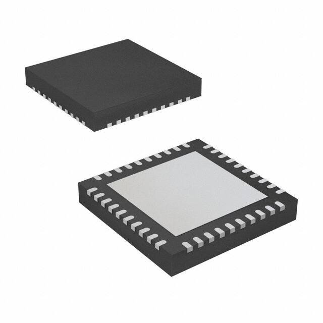
40-Lead QFN
Typical Application Circuit
VIN
GATE1
VIN_SNS
CS1
FLG
GND1
VDD
OVP1
VDD1
FLT1
VDD2
FDBK1
VDD3
PWMD1
GATE2
PWMD2
CS2
PWMD3
REF1
HV9989
REF2
GND2
OVP2
FLT2
REF3
FDBK2
EN
CLK
GATE3
GND
CS3
COMP1
GND3
OVP3
COMP2
FLT3
COMP3
SKIP
2014 Microchip Technology Inc.
SC
FDBK3
DS20005296B-page 3
�HV9989
1.0
ELECTRICAL
CHARACTERISTICS
ABSOLUTE MAXIMUM RATINGS †
VIN to GND ........................................................ -0.5V to +45V
VDD to GND, VDD 1-3 to GND ..........................--0.3V to +10V
All other pins to GND ......................... ....-0.3V to (VDD + 0.3V)
Operating temperature ....................................-40°C to +85°C
Storage temperature .....................................-65°C to +150°C
Continuous power dissipation (TA = +25°C).............4000 mW
† Notice: Stresses above those listed under “Absolute Maximum Ratings” may cause permanent damage to the device.
This is a stress rating only and functional operation of the
device at those or any other conditions, above those indicated in the operational listings of this specification, is not
implied. Exposure to maximum rating conditions for extended
periods may affect device reliability.
1.1
ELECTRICAL SPECIFICATIONS
TABLE 1-1:
Symbol
ELECTRICAL CHARACTERISTICS (SHEET 1 OF 3)1
Parameter
Note
Min
Typ
Max
Units Conditions
Input
VINDC
Input DC supply voltage
1
10
—
40
V
IINSD
Shut-down mode supply
current
1
—
—
500
μA
—
—
—
4.5
mA
1
7.0
—
8.1
V
Supply current
IIN
DC input voltage
EN = 0.8V
EN ≥ 2.0V; PWMD1 = PWMD2
= PWMD3 = GND
Internal Regulator
Internally regulated voltage
VDD
Load regulation
∆ VDD
—
—
—
80
mV
UVLO
VDD under voltage lockout
threshold
—
5.9
—
6.4
V
UVLOHYST
VDD under voltage hysteresis
—
-
500
-
mV
VIN= 11V; EN = GND;
External IDD = 30mA
VIN= 11V; EN = GND;
External IDD(A) = 10mA,
IDD(B) = 30mA
∆ VDD = VDD(A) - VDD(B)
VDD falling
VDD rising
PWM Dimming (PWMD1, PWMD2 and PWMD3)
VPWMD(lo) PWMD input low voltage
1
—
—
0.8
V
—
VPWMD(hi) PWMD input high voltage
1
2.0
—
—
V
—
RPWMD
PWMD pull down resistor
—
80
—
160
kΩ
Td
Delay time to PWMD latch
2
50
—
150
ns
—
DMAX inhibit delay
2
—
400
—
ns
—
TDP
Note 1:
2:
VPWMD = 5.0V
Applies over the full operating ambient temperature range of 0°C < TA < +85°C.
For design guidance only.
DS20005296B-page 4
2014 Microchip Technology Inc.
�HV9989
TABLE 1-1:
Symbol
ELECTRICAL CHARACTERISTICS (CONTINUED) (SHEET 2 OF 3)1
Parameter
Note
Min
Typ
Max
Units Conditions
Gate short circuit current,
sourcing
2
0.2
—
—
A
Gate sinking current
2
0.4
—
—
A
Gate (GATE1, GATE2 and GATE3)
ISOURCE
ISINK
VGATE = 0V
VGATE = VDD
TRISE
Gate output rise time
—
—
50
85
ns
CGATE = 1.0nF
TFALL
Gate output fall time
—
—
25
45
ns
CGATE = 1.0nF
DMAX
Maximum duty cycle
2
—
91
—
%
1
4.7
—
5.4
V
1
210
—
460
ns
—
Over-voltage Protection (OVP1, OVP2 and OVP3)
VOVP,rising Over-voltage rising trip point
OVP rising
Current Sense (CS1, CS2 and CS3)
TBLANK
Leading edge blanking
Delay to GATE
TDELAY
—
—
—
250
ns
—
50mV overdrive to the current
sense comparator
Slope Compensation (SC)
CSC(EFF)
∆VSC
Effective capacitance
2
0.9
1.0
1.1
nF
VDD-to-SC voltage drop
1
1.25
—
3.25
V
1.0
—
MHz
—
RSC = 120kΩ
Internal Transconductance Opamp (Gm1, Gm2 and Gm3)
GB
Gain bandwidth product
2
—
AV
Open loop DC gain
—
65
—
—
dB
COMP-to-CS divider ratio
2
—
1/12
—
—
KCOMP
VCM
75pF capacitance at COMP pin
Output open
—
Input common-mode range
2
-0.3
—
3.0
V
—
VO
Output voltage range
2
0.7
—
6.75
V
—
Gm
Transconductance
—
500
—
700
μA/V
—
VOFFSET
Input offset voltage
—
-5.0
—
5.0
mV
—
Input bias current
2
—
0.5
1.0
nA
IBIAS
TR
Recovery delay
—
FDBK = 0V, REF = 0.5V,
PWMD rising
2
—
120
—
ns
Oscillator frequency
—
—
500
—
kHz
KSW
Oscillator divider ratio
2
—
12
—
-
—
Phi1
GATE1-GATE2 phase delay
2
—
120
—
°
—
Phi1
GATE1-GATE3 phase delay
2
—
240
—
°
—
Oscillator (CLOCK)
fOSC1
FCLOCK = 6.0MHz
Oscillator (CLOCK)
TOFF
CLOCK low time
2
50
—
—
ns
—
TON
CLOCK high time
2
50
—
—
ns
—
VCLOCK,HI CLOCK input high
1
2.0
—
—
V
—
VCLOCK,L CLOCK input low
O
1
—
—
0.8
V
—
Note 1:
2:
Applies over the full operating ambient temperature range of 0°C < TA < +85°C.
For design guidance only.
2014 Microchip Technology Inc.
DS20005296B-page 5
�HV9989
ELECTRICAL CHARACTERISTICS (CONTINUED) (SHEET 3 OF 3)1
TABLE 1-1:
Symbol
Parameter
Note
Min
Typ
Max
Units Conditions
TRISE,FAU Fault output rise time
LT
—
—
—
300
ns
TFALL,FAU Fault output fall time
LT
—
—
—
200
ns
1
400
—
800
ns
—
—
Disconnect Driver (FLT1, FLT2 and FLT3)
330 pF capacitor at FLTx pin
330 pF capacitor at FLTx pin
Short Circuit Protection (all three channels)
TBLANK,S Blanking time
C
GSC
Gain for short circuit
comparator
—
1.9
2.0
2.1
—
Vomin
Minimum current limit
threshold
2
0.15
—
—
V
TOFF
Propagation time for short
circuit detection
—
—
—
250
ns
—
—
10
—
μA
—
2
—
4.0
—
V
—
REF = GND
FDBK = 2 • REF + 0.1V
HICCUP timer
Current source at SKIP pin
IHC,SOUR
used for hiccup mode proCE
tection
∆VCAP
SKIP voltage swing
Low output detection (OVP1, OVP2, OVP3, VIN_SNS, FLG)
VOVP_OS_ OVP offset voltage
F
1
-25
—
25
mV
VOVP_OS_ OVP offset voltage
R
—
40
—
70
mV
VFLG(LOW FLG low voltage
)
—
0
—
0.4
V
2
-0.3
—
5.0
V
VIN_CM
Note 1:
2:
Input common-mode range
OVP falling
OVP rising
I(FLG) = 1.0mA
—
Applies over the full operating ambient temperature range of 0°C < TA < +85°C.
For design guidance only.
1
TABLE 1-2:
THERMAL RESISTANCE
DS20005296B-page 6
Package
θja
40-Lead QFN
24°C/W
2014 Microchip Technology Inc.
�HV9989
2.0
PIN DESCRIPTION
The descriptions of the pins are listed in Table 2-1.
TABLE 2-1:
Pin #
PIN DESCRIPTION (SHEET 1 OF 2)
Name
Description
VDD1
Power supply pin for channel 1. It can either be connected to the VDD pin or supplied
with an external power supply. It must be bypassed with a low ESR capacitor to their
respective GND1 (at least 0.1 μF). All VDD pins (VDD, VDD1-3) must be connected
together externally.
2
FLT1
Drives external disconnect switches. The disconnect switches are used to protect the
LEDs in case of fault conditions, and also help to provide excellent PWM dimming
response by disconnecting and reconnecting the LEDs from the output capacitor during
PWM dimming.
3
CS1
Senses the source current of the external power FET used with channel 1. It includes a
built-in 210 ns (min) blanking timer.
4
COMP1
Stable closed loop control can be accomplished by connecting a compensation network
between the COMP pin and its GND.
5
FDBK1
Provides output current feedback for channel 1 by using a current sense resistor.
6
REF1
The voltage at this pin sets the output current level for channel 1. Recommended voltage
range for this pin is 0V-1.25V.
7
OVP1
Provides the over voltage protection for the converter. When the voltage at this pin
exceeds 5V, channel 1 of the HV9989 is turned off. The fault is reset by re-enabling the
IC using the EN pin.
8
VIN
Input of the internal 40V linear regulator.
9
VDD
Output of the linear regulator. It maintains a regulated 7.75V as long as the voltage of the VIN
pin is between 10 and 40V. It must be bypassed with a low ESR capacitor to GND (at least 0.1
μF). This pin can be used as a power supply for the three channels.
10
EN
When the pin is pulled below 0.8V, the IC goes into a standby mode and draws minimal current.
11
GND
12
COMP2
Stable closed loop control can be accomplished by connecting a compensation network
between the COMP pin and its GND.
13
REF2
The voltage at this pin sets the output current level for channel 2. Recommended voltage
range for this pin is 0-1.25V.
14
OVP2
Provides the over voltage protection for the converter. When the voltage at this pin
exceeds 5V, channel 2 of the HV9989 is turned off. The fault is reset by re-enabling the
IC using the EN pin.
15
SKIP
Programs the hiccup timer for short circuit fault on any of the three channels. A capacitor
to GND programs the hiccup time.
16
SC
17
PWMD1
Used to PWM dim channel 1.
18
PWMD2
Used to PWM dim channel 2.
19
PWMD3
Used to PWM dim channel 3.
20
NC
21
VIN_SNS
22
FLG
Open-drain logic output reporting a high-impedance state in the case of any of the OVP
1-3 voltages falling below the VIN_SNS voltage. A hysteresis is added at VIN_SNS to
avoid oscillation.
23
CLK
Clock input for the HV9989. The input to the CLK pin should be a TTL compatible square
wave signal. The three channels will switch at 1/12th the switching frequency of the signal applied at the CLK pin.
1
Ground connection for the common circuitry in the HV9989.
Sets the current to program slope compensation voltage ramp at the three CS inputs.
Connect a resistor to GND.
No connection.
When voltage at this pin exceeds any of the voltages at OVP 1-3, the high-impedance
state is issued at the FLG output.
2014 Microchip Technology Inc.
DS20005296B-page 7
�HV9989
TABLE 2-1:
PIN DESCRIPTION (CONTINUED) (SHEET 2 OF 2)
Pin #
Name
Description
24
OVP3
Provides the over voltage protection for the converter. When the voltage at this pin
exceeds 5V, channel 3 of the HV9989 is turned off. The fault is reset by re-enabling the
IC using the EN pin.
25
REF3
The voltage at this pin sets the output current level for channel 3. Recommended voltage
range for this pin is 0V-1.25V.
26
FDBK3
Provides output current feedback for channel 3 by using a current sense resistor.
27
COMP3
Stable closed loop control can be accomplished by connecting a compensation network
between the COMP pin and its GND.
28
CS3
Used to sense the source current of the external power FET used with channel 3. It
includes a built-in 210 ns (min) blanking timer.
FLT3
Used to drive external disconnect switches. The disconnect switches are used to protect
the LEDs in case of fault conditions and also help to provide excellent PWM dimming
response by disconnecting and reconnecting the LEDs from the output capacitor during
PWM dimming.
30
VDD3
Power supply pin for channel 3. It can either be connected to the VDD pin or supplied
with an external power supply. It must be bypassed with a low ESR capacitor to their
respective GND3 (at least 0.1 μF). All VDD pins (VDD, VDD1-3) must be connected
together externally.
31
GATE3
Output gate driver for the external N-channel power MOSFET.
32
GND3
Ground return for channel 3. It is recommended that all the GNDs of the IC be connected
together in a STAR connection at the input GND terminal to ensure best performance.
33
VDD2
Power supply pin for channel 2. It can either be connected to the VDD pin or supplied
with an external power supply. It must be bypassed with a low ESR capacitor to their
respective GND2 (at least 0.1 μF). All VDD pins (VDD, VDD1-3) must be connected
together externally.
34
GND2
Ground return for channel 2. It is recommended that all the GNDs of the IC be connected
together in a STAR connection at the input GND terminal to ensure best performance.
35
GATE2
Output gate driver for the external N-channel power MOSFET.
29
36
FLT2
Used to drive external disconnect switches. The disconnect switches are used to protect
the LEDs in case of fault conditions and also help to provide excellent PWM dimming
response by disconnecting and reconnecting the LEDs from the output capacitor during
PWM dimming.
37
CS2
Used to sense the source current of the external power FET used with channel 2. It
includes a built-in 210 ns (min) blanking timer.
38
FDBK2
Provides output current feedback for channel 2 by using a current sense resistor.
39
GND1
Ground return for channel 1. It is recommended that all the GNDs of the IC be connected
together in a STAR connection at the input GND terminal to ensure best performance.
40
GATE1
Output gate driver for the external N-channel power MOSFET.
DS20005296B-page 8
2014 Microchip Technology Inc.
�HV9989
3.0
FUNCTIONAL DESCRIPTION
3.1
Power Topology
HV9989 is a three-channel, switch-mode converter,
LED driver designed to control a continuous conduction
mode boost or SEPIC device in a constant frequency
mode. The IC includes an internal linear regulator,
which operates from 10 to 40V input voltages. This
device can also be powered directly using the VDD
pins and bypassing the internal linear regulator.
HV9989 includes features typically required in LED
drivers such as open LED protection, output short circuit protection, linear and PWM dimming, programmable input current limiting and accurate control of the
LED current. A high current gate drive output enables
the controller to be used in high power converters.
HV9989 is ideally suited for back-light applications
using either RGB or multi-channel white LED
configurations.
3.2
Power Supply to the IC (VIN, VDD,
VDD1-3)
The HV9989 can be powered directly from its VIN pin
that takes a voltage up to 40V. When a voltage is
applied at the VIN pin, the HV9989 tries to maintain a
constant 7.75V (typ) at the VDD pin. The regulator also
has a built in under-voltage lockout which shuts off the
IC if the voltage at the VDD pin falls below the UVLO
threshold. By connecting this VDD pin to the individual
VDD pins of the three channels, the internal regulator
can be used to power all three channels in the IC.
In case the internal regulator is not utilized, an external
power supply (7-9V) can be used to power the IC. In
this case, the power supply is directly connected to the
VDD pins and the VIN pin is left unconnected.
All four VDD pins must be bypassed by a low ESR
capacitor (≥0.1 µF) to provide a low impedance path for
the high frequency current of the output gate driver.
These capacitors must be referenced to the individual
grounds for proper noise rejection. Also, in all cases,
the four VDD pins must be connected together
externally.
The input current drawn from the external power supply
(or VIN pin) is a sum of the 4 mA current drawn by the
all the internal circuitry (for all three channels) and the
current drawn by the gate drivers (which in turn
depends on the switching frequency and the gate
charge of the external FET).
I IN =
4mA + Q G1 + Q G2 + Q G3 f s
2014 Microchip Technology Inc.
In the preceding equation, fS is the switching frequency
of the converters and QG1-3 are the gate charges of the
external FETs (which can be obtained from the FET
data sheets).
The EN pin is a TTL-compatible input used to disable
the IC. Pulling the EN pin to GND will shut down the IC
and reduce the quiescent current drawn by the IC to be
lower than 500 μA. If the enable function is not
required, the EN pin can be connected to VDD.
3.3
Clock Input (CLK)
The switching frequency of the converters are set by
using a TTL-compatible square wave input at the CLK
pin. The switching frequencies of the three converters
will be 1/12th the frequency of the external clock.
3.4
Current Sense (CS1-3)
The current sense input is used to sense the source
current of the switching FET. The CS input of the
HV9989 includes a built-in 100 ns (minimum) blanking
time to prevent spurious turn off due to the initial current
spike when the FET turns on.
The IC includes an internal resistor divider network,
which steps down the voltage at the COMP pins by a
factor of 12 (including the internal diode drop). This
stepped-down voltage is given to one of the
comparators as the current reference.
It is recommended that the sense resistor RCS be chosen so as to provide about 250 mV current sense signal.
3.5
Slope Compensation
For continuous conduction mode converters operating in
the Constant Frequency mode, slope compensation
becomes necessary to ensure stability of the peak current mode controller, if the operating duty cycle is greater
than 0.5. Choosing a slope compensation which is one
half of the down slope of the inductor current ensures
that the converter will be stable for all duty cycles.
Slope compensation in the HV9989 can be programmed by a single resistor at SC input common for
all three channels. Assuming a down slope of DS (A/
ms) for the inductor current, the SC resistor can be
computed as:
2 VDD – V SC
11V
R SC = ------------------------------------------------------------- ----------------------------------------------6
DS 10 R CS C SC EFF DS R CS C SC EFF
where RCS is the current sense resistor at the CSX
inputs.
DS20005296B-page 9
�HV9989
3.6
Control of the LED Current
The LED currents in the HV9989 are controlled in a
closed-loop manner. The current references which set
the three LED currents are provided at the REF pins
(REF1-3). This reference voltage is compared to the
FDBK voltages (FDBK1-3) which sense the LED currents in the three channels using current sense resistors.
The
HV9989
includes
three
1MHz
transconductance amplifiers with tri-state outputs,
which are used to close the feedback loops and provide
accurate current control. The compensation networks
are connected at the COMP pins (COMP1-3).
The outputs of the op amps are buffered and connected
to the current sense comparators using 12:1 dividers.
The buffer helps to prevent the integrator capacitor from
discharging during the PWM dimming state.
The outputs of the op amps are controlled by the signal
applied to the PWMD pins (PWMD1-3). When PWMD
is high, the output of the op amp is connected to the
COMP pin. When PWMD is low, the output is left open.
This enables the integrating capacitor to hold the
charge when the PWMD signal has turned off the gate
drive. When the IC is enabled, the voltage on the integrating capacitor will force the converter into steady
state almost instantaneously.
3.7
PWM Dimming
PWM dimming in HV9989 can be accomplished using
a TTL-compatible square wave source at the PWMD13 pins.
HV9989 has an enhanced PWM dimming capability,
which allows PWM dimming to widths less than one
switching cycle with no drop in the LED current.
The enhanced PWM dimming performance of the
HV9989 can be best explained by considering typical
boost converter circuits without this functionality. When
the PWM dimming pulse becomes very small (less than
one switching cycle for a DCM design or less than a few
switching cycles for a CCM design), the boost converter is turned off before the input current can reach its
steady state value. This causes the input power to
drop, which is manifested in the output as a drop in the
LED current (Figure 3-1 and Figure 3-2 for a CCM
design).
FIGURE 3-1:
Due to the offset voltage of the short circuit comparator,
as well as the non-linearity of the X2 gain stage, pulling
the REF pin very close to GND would cause the internal short circuit comparator to trigger and shut down
the IC. To overcome this, the output of the gain stage is
limited to 125mV (minimum), allowing the REF pin to
be pulled all the way to 0V without triggering the short
circuit comparator.
This control IC is a peak current mode controller; therefore, pulling the REF pin to zero will
not cause the LED current to go to zero. The
converter will still be operating at its minimum
on-time causing a very small current to flow
through the LEDs. To get zero LED current,
the PWMD input has to be pulled to GND.
DS20005296B-page 10
PWM DIMMING WITH
DIMMING ON-TIME FAR
GREATER THAN ONE
SWITCHING TIME PERIOD
PWMD
Linear Dimming
Linear dimming can be accomplished in the HV9989 by
varying the voltages at the REF pins. Note that since
the HV9989 is a peak current mode controller, it has a
minimum on-time for the GATE outputs. This minimum
on-time will prevent the converters from completely
turning off even when the REF pins are pulled to GND.
Thus, linear dimming cannot accomplish true zero LED
current. To get zero LED current, PWM dimming has to
be used. Note that different signals can be connected
to the three REF pins if desired, and they need not be
connected together.
Note:
3.8
IO(SS)
ILED
IINDUCTOR
FIGURE 3-2:
IO(SS)
PWM DIMMING WITH
DIMMING ON-TIME
EQUAL TO ONE
SWITCHING TIME PERIOD
PWMD
IO(SS)
ILED
IINDUCTOR
IL(SS)
In the above figures, IO(SS) and IL(SS) refer to the
steady state values (PWMD = 100%) for the output current and inductor current respectively. As can be seen,
the inductor current does not rise enough to trip the CS
comparator. This causes the closed loop amplifier to
lose control of the LED current and COMP rails to VDD.
2014 Microchip Technology Inc.
�HV9989
In the HV9989, however, this problem is overcome by
keeping the boost converter ON, even though PWMD
has gone to zero to ensure enough power is delivered
to the output.
capacitor should be large enough so that it can absorb
the inductor energy without a significant change of the
voltage across it. If the capacitor voltage change is significant, it would cause a turn-on spike in the inductor
current when PWMD goes high.
Thus, the amplifier still has control over the LED current
and the LED current will be in regulation as shown in
Figure 3-3.
3.9
FIGURE 3-3:
During the Power-on Reset (POR) state upon startup,
both GATE and FLT outputs are disabled. The COMP
pins and the SKIP pin are pulled to GND.
PWM DIMMING WITH
DIMMING ON-TIME EQUAL
TO ONE SWITCHING TIME
PERIOD WITH HV9989
When an output over-current condition is detected in
any individual channel, the corresponding GATE and
FLT outputs are disabled, and the corresponding
COMP output is pulled to GND. The remaining channel
GATE, FLT and COMP outputs are not affected. The
SKIP pin is pulled to GND. If pulling FLT low clears the
over-current condition in the faulty channel, and once
the voltage at the SKIP pin falls below 1.0V, the capacitor at the SKIP pin is released and is charged slowly by
a 10 μA current source. Once the capacitor is charged
to 5.0V, the COMP pins are released and GATE and
FLT pins are allowed to turn on. If the hiccup time is
long enough, it will ensure that the compensation networks are all completely discharged and that the
converters start at minimum duty cycle.
PWMD
IO(SS)
ILED
IL(SS)
IINDUCTOR
SKIP Timer Logic
Note that the GATE output is not limited by its maximum duty cycle, DMAX, past the PWMD signal trailing
edge. The gate is kept on until the corresponding CS
reference is met by IINDUCTOR.
When the PWM signal is high, the GATE and FLT pins
are enabled and the output of the transconductance op
amp is connected to the external compensation network. Thus, the internal amplifier controls the output
current. When the PWMD signal goes low, the output of
the transconductance amplifier is disconnected from
the compensation network. Thus, the integrating
capacitor maintains the voltage across it. The FLT pin
goes low, turning off the disconnect switch. However,
the boost FET is kept running.
If, during the charging phase of the SKIP output, an
over-current condition is detected in another channel,
the SKIP pin is pulled to GND again, and the ramp
starts over. All faulty channels make an attempt to
recover at the same time when the FLT capacitor is
charged to 5.0V. Operation of other “good” channel(s)
is not affected by the SKIP pin status.
The hiccup timing capacitor can be programmed as:
10A t HICCUP
C RAMP = --------------------------------------4V
Note that disconnecting the LED load during PWM dimming causes the energy stored in the inductor to be
dumped into the output capacitor. The chosen filter
FIGURE 3-4:
DEEP PWM DIMMING PERFORMANCE: LED CURRENT MAINTAINED IN REGULATION
6.5µs
Dimming Input
400ns
Inductor Current
LED Current
2014 Microchip Technology Inc.
DS20005296B-page 11
�HV9989
3.10
Short Circuit Protection
When a short circuit condition is detected (output current becomes higher than twice the steady state current), the GATE and FLT outputs are pulled low. As
soon as the disconnect FET is turned off, the output
current goes to zero and the short circuit condition disappears. At this time, the hiccup timer is started. Once
the timing is complete, the converter attempts to
restart. If the fault condition still persists, the converter
shuts down and goes through the cycle again. If the
fault condition is cleared (due to a momentary output
short) the converter will start regulating the output current normally. This allows the LED driver to recover
from accidental shorts without having to reset the IC.
During short circuit conditions, there are two conditions
that determine the hiccup time.
The first condition is the time required to discharge the
compensation capacitors. Assuming a pole-zero R-C
network at the COMP pin (series combination of RZ
and CZ in parallel with CC),
t COMP n = 3 R Zn C Zn
3.11
False Triggering of the Short
Circuit Comparator During PWM
Dimming
During PWM dimming, the parasitic capacitance of the
LED string causes a spike in the output current when
the disconnect FET is turned on. If this spike is
detected by the short circuit comparator, it will cause
the IC to falsely detect an over current condition and
shut down.
In the HV9989, to prevent these false triggers, there is
a built-in 500 ns blanking network for the short circuit
comparator. This blanking network is activated when
the PWMD input goes high. Thus, the short circuit comparator will not see the spike in the LED current during
the PWM dimming turn-on transition. Once the blanking timer is complete, the short circuit comparator will
start monitoring the output current. Thus, the total delay
time for detecting a short circuit will depend on the condition of the PWMD input.
If the output short circuit exists before the PWM-dimming signal goes high, the total detection time will be:
t DETECT1 = tBLANK + t DELAY 950ns max
where n refers to the channel number.
If the compensation networks are only type 1 (single
capacitor), then:
If the short circuit occurs when the PWM dimming signal is already high, the time to detect will be:
tCOMP n = 3 300 C Cn
t = t 250ns max
Thus, the maximum compensation time required can
be computed as:
tCOMP max = max t COMP1 ,t COMP2 ,tCOMP3
The second condition is the time required for the inductors to completely discharge following a short circuit.
This time can be computed as:
t ind n = --- L n COn
4
where L and CO are the input inductor and output
capacitor of each power stage.
Thus, the maximum time required to discharge the
inductors can be computed as:
t IND MAX = max t IND1 ,t IND2 ,t IND3
The hiccup time is then chosen as:
t HICCUP = max tCOMP MAX ,tIND MAX
DS20005296B-page 12
3.12
Over-voltage Protection
The HV9989 provides latching over-voltage protection.
When the load is disconnected in a boost converter, the
output voltage rises as the output capacitor starts
charging. When the output voltage reaches the OVP
rising threshold, the HV9989 detects an over-voltage
condition and turns off the converter. The converter is
turned back on only when the EN pin is toggled.
In most designs, the lower threshold voltage of the
over-voltage protection when the converter will be
turned on will be more than the LED string voltage.
Thus, when the LED load is reconnected to the output
of the converter, the voltage differential between the
actual output voltage and the LED string voltage will
cause a spike in the output current when the FLT signal
goes high. This causes a short circuit to be detected
and the HV9989 will go into short circuit protection.
This behavior continues until the output voltage
becomes lower than the LED string voltage, at which
point no fault will be detected and normal operation of
the circuit will commence.
2014 Microchip Technology Inc.
�HV9989
3.13
Input-Output Voltage Comparator
VIN_SNS. The FLG output recovers into the lowimpedance state when the faulty OVP input voltage
becomes greater than VIN_SNS by a 55mV hysteresis.
The HV9989 includes a circuit for detecting any of the
three boost converter output voltages falling below the
input voltage. The input voltage is monitored at the
VIN_SNS input using a resistor divider having the
same ratio as the OVP1-3 resistor dividers. An opendrain FLG output reports a high impedance state when
the voltage at either of the OVP1-3 inputs falls below
FIGURE 3-5:
A pull-up resistor should be added at FLG. The FLG
output can sink up to 1.0mA.
TIMER CIRCUIT
POR
SCDA
SCDB
SCDC
0.1V
S
+
Fault
R
-
5.0V
SKIP
Q
10µA
+
-
DIS
Fault
FCA
2014 Microchip Technology Inc.
DS20005296B-page 13
�HV9989
FIGURE 3-6:
INTERNAL BLOCK DIAGRAM
EN
VIN
Bandgap
CLK
VDD
REF
0
120
240
1/12
Linear
Regulator
CLKA
CLKB
CLKC
UVLO
VDD2
POR
AGND
PWMDA
CLKA
S
Q
R
Q
S
GATE1
Q
R
FCA
OVA
Q
CLKA
FG2
RC = 50ns
I(SC)*k
FG3
Blanking
+
-
Td
PWMD1
PWMDA
FLT1
PWMDA
OVA
FCA
PGND1
MAXDUTYA
DMAX
Logic A
1
PWMDA
R
SCDA
+
S
Q
R
Q
FDBK1
2
+
IN
-
REF1
11R
-
Blanking
-
FG1
+
REF
1
1
1
+
PWMDA
COMP1
POR
OVA
DIS
MAXDUTYB
PWMDB
Td
PWMDB_dly
1
PWMDB_dly
CLKB
S
Q
R
Q
PWMDB
PWMD2
S
GATE2
Q
R
FCB
OVB
Q
CLKB
I(SC)*k
PWMDB
OVB
FCB
FLT2
-
REF
Blanking
-
CLKB
PGND2
S
Q
R
Q
2
CLKB
PWMDB
FG2
2
MAXDUTYB
DMAX
Logic B
2
PWMDB
R
REF2
11R
+
1
POR
OVB
SCDB
-
Blanking
-
Timer
FDBK2
2
+
FCA
SKIP
CS2
CLKB
CLKB
+
RC = 50ns
+
+
IN
OVP2
CS1
CLKA
CLKA
CLKA
PWMDA_dly
CLKA
PWMDA
OVP1
VDD3
MAXDUTYA
PWMDA_dly
FG1
FLG
VDD1
PWMDB
FCB
COMP2
FCC
DIS
MAXDUTYC
2
PWMDC
PWMDC_dly
I(SC)
Current
Mirror
SC
CLKC
S
Q
R
Q
GATE3
Q
S
R
FCC
OVC
Q
CLKC
RC = 50ns
I(SC)*k
Blanking
+
Td
PWMDC_dly
PWMD3
CLKC
3
MAXDUTYC
DMAX
Logic C
3
R
S
POR
R
+
REF
11R
Q
Q
REF3
+
-
1
SCDC
IN
+
3
PWMDC
PWMDC
OVC
FCC
OVP3
CS3
PGND3
CLKC
CLKC
PWMDC
PWMDC
FLT3
CLKC
+
-
FDBK3
2
Blanking
FG3
PWMDC
COMP3
DIS
OVC
3
VIN_SNS
DS20005296B-page 14
2014 Microchip Technology Inc.
�HV9989
4.0
PACKAGING INFORMATION
4.1
Package Marking Information
40-Lead QFN
XXXXXXX
XXXXXXXX
XXXXXX e3
YYWWNNN
Legend: XX...X
Y
YY
WW
NNN
e3
*
Note:
Example
HV9989 e3
YYWWNNN
Product Code or Customer-specific information
Year code (last digit of calendar year)
Year code (last 2 digits of calendar year)
Week code (week of January 1 is week ‘01’)
Alphanumeric traceability code
Pb-free JEDEC designator for Matte Tin (Sn)
This package is Pb-free. The Pb-free JEDEC designator ( e3 )
can be found on the outer packaging for this package.
In the event the full Microchip part number cannot be marked on one line, it will
be carried over to the next line, thus limiting the number of available
characters for customer-specific information.
2014 Microchip Technology Inc.
DS20005296B-page 15
�HV9989
40 Lead QFN
D
40
D2
40
1
1
Note 1
(Index Area
D/2 x E/2)
Note 1
(Index Area
D/2 x E/2)
e
E
E2
b
View B
Top View
Bottom View
Note 3
θ
L
A3
A
Seating
Plane
L1
Note 2
A1
Side View
View B
Notes:
1: A Pin 1 identifier must be located in the index area indicated. The Pin 1 identifier can be: a molded mark/
identifier; an embedded metal marker; or a printed indicator.
2: Depending on the method of manufacturing, a maximum of 0.15mm pullback (L1) may be present.
3: The inner tip of the lead may be either rounded or square.
4: For the most current package drawings, please see the Microchip Packaging Specification located at
http://www.microchip.com/packaging
Symbol
Dimension
(mm)
A
A1
A3
b
D
D2
E
E2
e
MIN
0.80
0.00
0.20
0.18
5.85*
1.05
5.85*
1.05
0.50
NOM
0.90
0.02
0.25
6.00
-
6.00
-
MAX
1.00
0.05
REF
0.30
6.15*
4.45
6.15*
4.45
BSC
L
L1
θO
0.30†
0.00
0
0.40†
-
-
0.50†
0.15
14
JEDEC Registration MO-220, Variation VJJD-6, Issue K, June 2006.
* This dimension is not specified in the JEDEC drawing.
† This dimension differs from the JEDEC drawing.
Drawings not to scale.
DS20005296B-page 16
2014 Microchip Technology Inc.
�HV9989
APPENDIX A:
REVISION HISTORY
Revision A (May 2014)
• Original Release of this Document.
Revision B (September 2014)
• Updated template to the Microchip template
• Updated the package marking information
2014 Microchip Technology Inc.
DS20005296B-page 17
�HV9989
THE MICROCHIP WEB SITE
CUSTOMER SUPPORT
Microchip provides online support via our WWW site at
www.microchip.com. This web site is used as a means
to make files and information easily available to
customers. Accessible by using your favorite Internet
browser, the web site contains the following
information:
Users of Microchip products can receive assistance
through several channels:
• Product Support – Data sheets and errata,
application notes and sample programs, design
resources, user’s guides and hardware support
documents, latest software releases and archived
software
• General Technical Support – Frequently Asked
Questions (FAQ), technical support requests,
online discussion groups, Microchip consultant
program member listing
• Business of Microchip – Product selector and
ordering guides, latest Microchip press releases,
listing of seminars and events, listings of
Microchip sales offices, distributors and factory
representatives
•
•
•
•
Distributor or Representative
Local Sales Office
Field Application Engineer (FAE)
Technical Support
Customers
should
contact
their
distributor,
representative or Field Application Engineer (FAE) for
support. Local sales offices are also available to help
customers. A listing of sales offices and locations is
included in the back of this document.
Technical support is available through the web site
at: http://microchip.com/support
CUSTOMER CHANGE NOTIFICATION
SERVICE
Microchip’s customer notification service helps keep
customers current on Microchip products. Subscribers
will receive e-mail notification whenever there are
changes, updates, revisions or errata related to a
specified product family or development tool of interest.
To register, access the Microchip web site at
www.microchip.com. Under “Support”, click on
“Customer Change Notification” and follow the
registration instructions.
DS20005296B-page 18
2014 Microchip Technology Inc.
�HV9989
PRODUCT IDENTIFICATION SYSTEM
To order or obtain information, e.g., on pricing or delivery, refer to the factory or the listed sales office.
PART NO.
Device
XX
X
Package Environmental
Options
X
Reel
Device:
HV9989 = Three-channel CCM/DCM Boost LED Driver
with Sub-microsecond PWM dimming
Package:
K6
= 40-lead (6x6) QFN
Environmental
G
= Lead (Pb)-free/ROHS-compliant package
Reel:
Examples:
a)
HV9989K6-G:
40-lead QFN package,
490/Tray.
b)
HV9989K6-G-M935:
40-lead QFN package,
2000/Reel.
(nothing) = Tray
M935
= Reel
2014 Microchip Technology Inc.
DS20005296B-page 19
�HV9989
DS20005296B-page 20
2014 Microchip Technology Inc.
�Note the following details of the code protection feature on Microchip devices:
•
Microchip products meet the specification contained in their particular Microchip Data Sheet.
•
Microchip believes that its family of products is one of the most secure families of its kind on the market today, when used in the
intended manner and under normal conditions.
•
There are dishonest and possibly illegal methods used to breach the code protection feature. All of these methods, to our
knowledge, require using the Microchip products in a manner outside the operating specifications contained in Microchip’s Data
Sheets. Most likely, the person doing so is engaged in theft of intellectual property.
•
Microchip is willing to work with the customer who is concerned about the integrity of their code.
•
Neither Microchip nor any other semiconductor manufacturer can guarantee the security of their code. Code protection does not
mean that we are guaranteeing the product as “unbreakable.”
Code protection is constantly evolving. We at Microchip are committed to continuously improving the code protection features of our
products. Attempts to break Microchip’s code protection feature may be a violation of the Digital Millennium Copyright Act. If such acts
allow unauthorized access to your software or other copyrighted work, you may have a right to sue for relief under that Act.
Information contained in this publication regarding device
applications and the like is provided only for your convenience
and may be superseded by updates. It is your responsibility to
ensure that your application meets with your specifications.
MICROCHIP MAKES NO REPRESENTATIONS OR
WARRANTIES OF ANY KIND WHETHER EXPRESS OR
IMPLIED, WRITTEN OR ORAL, STATUTORY OR
OTHERWISE, RELATED TO THE INFORMATION,
INCLUDING BUT NOT LIMITED TO ITS CONDITION,
QUALITY, PERFORMANCE, MERCHANTABILITY OR
FITNESS FOR PURPOSE. Microchip disclaims all liability
arising from this information and its use. Use of Microchip
devices in life support and/or safety applications is entirely at
the buyer’s risk, and the buyer agrees to defend, indemnify and
hold harmless Microchip from any and all damages, claims,
suits, or expenses resulting from such use. No licenses are
conveyed, implicitly or otherwise, under any Microchip
intellectual property rights.
Trademarks
The Microchip name and logo, the Microchip logo, dsPIC,
FlashFlex, flexPWR, JukeBlox, KEELOQ, KEELOQ logo, Kleer,
LANCheck, MediaLB, MOST, MOST logo, MPLAB,
OptoLyzer, PIC, PICSTART, PIC32 logo, RightTouch, SpyNIC,
SST, SST Logo, SuperFlash and UNI/O are registered
trademarks of Microchip Technology Incorporated in the
U.S.A. and other countries.
The Embedded Control Solutions Company and mTouch are
registered trademarks of Microchip Technology Incorporated
in the U.S.A.
Analog-for-the-Digital Age, BodyCom, chipKIT, chipKIT logo,
CodeGuard, dsPICDEM, dsPICDEM.net, ECAN, In-Circuit
Serial Programming, ICSP, Inter-Chip Connectivity, KleerNet,
KleerNet logo, MiWi, MPASM, MPF, MPLAB Certified logo,
MPLIB, MPLINK, MultiTRAK, NetDetach, Omniscient Code
Generation, PICDEM, PICDEM.net, PICkit, PICtail,
RightTouch logo, REAL ICE, SQI, Serial Quad I/O, Total
Endurance, TSHARC, USBCheck, VariSense, ViewSpan,
WiperLock, Wireless DNA, and ZENA are trademarks of
Microchip Technology Incorporated in the U.S.A. and other
countries.
SQTP is a service mark of Microchip Technology Incorporated
in the U.S.A.
Silicon Storage Technology is a registered trademark of
Microchip Technology Inc. in other countries.
GestIC is a registered trademarks of Microchip Technology
Germany II GmbH & Co. KG, a subsidiary of Microchip
Technology Inc., in other countries.
All other trademarks mentioned herein are property of their
respective companies.
© 2014, Microchip Technology Incorporated, Printed in the
U.S.A., All Rights Reserved.
ISBN: 978-1-63276-579-6
QUALITY MANAGEMENT SYSTEM
CERTIFIED BY DNV
== ISO/TS 16949 ==
2014 Microchip Technology Inc.
Microchip received ISO/TS-16949:2009 certification for its worldwide
headquarters, design and wafer fabrication facilities in Chandler and
Tempe, Arizona; Gresham, Oregon and design centers in California
and India. The Company’s quality system processes and procedures
are for its PIC® MCUs and dsPIC® DSCs, KEELOQ® code hopping
devices, Serial EEPROMs, microperipherals, nonvolatile memory and
analog products. In addition, Microchip’s quality system for the design
and manufacture of development systems is ISO 9001:2000 certified.
DS20005296B-page 21
�Worldwide Sales and Service
AMERICAS
ASIA/PACIFIC
ASIA/PACIFIC
EUROPE
Corporate Office
2355 West Chandler Blvd.
Chandler, AZ 85224-6199
Tel: 480-792-7200
Fax: 480-792-7277
Technical Support:
http://www.microchip.com/
support
Web Address:
www.microchip.com
Asia Pacific Office
Suites 3707-14, 37th Floor
Tower 6, The Gateway
Harbour City, Kowloon
Hong Kong
Tel: 852-2943-5100
Fax: 852-2401-3431
India - Bangalore
Tel: 91-80-3090-4444
Fax: 91-80-3090-4123
Austria - Wels
Tel: 43-7242-2244-39
Fax: 43-7242-2244-393
Denmark - Copenhagen
Tel: 45-4450-2828
Fax: 45-4485-2829
Atlanta
Duluth, GA
Tel: 678-957-9614
Fax: 678-957-1455
Austin, TX
Tel: 512-257-3370
Boston
Westborough, MA
Tel: 774-760-0087
Fax: 774-760-0088
Chicago
Itasca, IL
Tel: 630-285-0071
Fax: 630-285-0075
Cleveland
Independence, OH
Tel: 216-447-0464
Fax: 216-447-0643
Dallas
Addison, TX
Tel: 972-818-7423
Fax: 972-818-2924
Detroit
Novi, MI
Tel: 248-848-4000
Houston, TX
Tel: 281-894-5983
Indianapolis
Noblesville, IN
Tel: 317-773-8323
Fax: 317-773-5453
Los Angeles
Mission Viejo, CA
Tel: 949-462-9523
Fax: 949-462-9608
New York, NY
Tel: 631-435-6000
San Jose, CA
Tel: 408-735-9110
Canada - Toronto
Tel: 905-673-0699
Fax: 905-673-6509
DS20005296B-page 22
Australia - Sydney
Tel: 61-2-9868-6733
Fax: 61-2-9868-6755
China - Beijing
Tel: 86-10-8569-7000
Fax: 86-10-8528-2104
China - Chengdu
Tel: 86-28-8665-5511
Fax: 86-28-8665-7889
China - Chongqing
Tel: 86-23-8980-9588
Fax: 86-23-8980-9500
China - Hangzhou
Tel: 86-571-8792-8115
Fax: 86-571-8792-8116
China - Hong Kong SAR
Tel: 852-2943-5100
Fax: 852-2401-3431
China - Nanjing
Tel: 86-25-8473-2460
Fax: 86-25-8473-2470
China - Qingdao
Tel: 86-532-8502-7355
Fax: 86-532-8502-7205
China - Shanghai
Tel: 86-21-5407-5533
Fax: 86-21-5407-5066
China - Shenyang
Tel: 86-24-2334-2829
Fax: 86-24-2334-2393
China - Shenzhen
Tel: 86-755-8864-2200
Fax: 86-755-8203-1760
China - Wuhan
Tel: 86-27-5980-5300
Fax: 86-27-5980-5118
China - Xian
Tel: 86-29-8833-7252
Fax: 86-29-8833-7256
India - New Delhi
Tel: 91-11-4160-8631
Fax: 91-11-4160-8632
India - Pune
Tel: 91-20-3019-1500
Japan - Osaka
Tel: 81-6-6152-7160
Fax: 81-6-6152-9310
Japan - Tokyo
Tel: 81-3-6880- 3770
Fax: 81-3-6880-3771
Korea - Daegu
Tel: 82-53-744-4301
Fax: 82-53-744-4302
Korea - Seoul
Tel: 82-2-554-7200
Fax: 82-2-558-5932 or
82-2-558-5934
France - Paris
Tel: 33-1-69-53-63-20
Fax: 33-1-69-30-90-79
Germany - Dusseldorf
Tel: 49-2129-3766400
Germany - Munich
Tel: 49-89-627-144-0
Fax: 49-89-627-144-44
Germany - Pforzheim
Tel: 49-7231-424750
Italy - Milan
Tel: 39-0331-742611
Fax: 39-0331-466781
Italy - Venice
Tel: 39-049-7625286
Malaysia - Kuala Lumpur
Tel: 60-3-6201-9857
Fax: 60-3-6201-9859
Netherlands - Drunen
Tel: 31-416-690399
Fax: 31-416-690340
Malaysia - Penang
Tel: 60-4-227-8870
Fax: 60-4-227-4068
Poland - Warsaw
Tel: 48-22-3325737
Philippines - Manila
Tel: 63-2-634-9065
Fax: 63-2-634-9069
Singapore
Tel: 65-6334-8870
Fax: 65-6334-8850
Taiwan - Hsin Chu
Tel: 886-3-5778-366
Fax: 886-3-5770-955
Spain - Madrid
Tel: 34-91-708-08-90
Fax: 34-91-708-08-91
Sweden - Stockholm
Tel: 46-8-5090-4654
UK - Wokingham
Tel: 44-118-921-5800
Fax: 44-118-921-5820
Taiwan - Kaohsiung
Tel: 886-7-213-7830
Taiwan - Taipei
Tel: 886-2-2508-8600
Fax: 886-2-2508-0102
Thailand - Bangkok
Tel: 66-2-694-1351
Fax: 66-2-694-1350
China - Xiamen
Tel: 86-592-2388138
Fax: 86-592-2388130
China - Zhuhai
Tel: 86-756-3210040
Fax: 86-756-3210049
03/25/14
2014 Microchip Technology Inc.
�


 工商网监
湘ICP备2023018690号
工商网监
湘ICP备2023018690号
