0
登录后你可以
  • 下载海量资料
  • 学习在线课程
  • 观看技术视频
  • 写文章/发帖/加入社区
会员中心
创作中心
发布
  • 发文章

  • 发资料

  • 发帖

  • 提问

  • 发视频

创作活动
JAN1N3017DUR-1/TR

JAN1N3017DUR-1/TR

  • 厂商:

    ACTEL(微芯科技)

  • 封装:

    DO213AB

  • 描述:

    VOLTAGE REGULATOR

  • 详情介绍
  • 数据手册
  • 价格&库存
JAN1N3017DUR-1/TR 数据手册
1N3016BUR-1 – 1N3045BUR-1 Available on commercial versions Qualified Levels: JAN, JANTX, and JANTXV 1 Watt Surface Mount Zener Diodes Qualified per MIL-PRF-19500/115 DESCRIPTION This surface mountable Zener diode series is similar to the 1N3016B-1 through 1N3045B-1 JEDEC registration in the DO-13 package except that it meets the surface mount DO-213AB outline. It is an ideal selection for applications of high density and low parasitic requirements. Due to its glass hermetic seal qualities and metallurgically enhanced internal construction, it is also well suited for high-reliability applications where it is available in JAN, JANTX, and JANTXV military qualifications. Lower voltages are also available in the 1N3821AUR-1 through 1N3828AUR-1 series (3.3 V to 7.5 V) in the same package (see separate data sheet). DO-213AB (MELF, LL41) Package Important: For the latest information, visit our website http://www.microsemi.com. FEATURES • • Leadless surface mount equivalents to the JEDEC registered 1N3016 through 1N3045 number series. Zener voltage range: 6.8 volts to 110 volts. • Hermetically sealed, double plug glass construction. • • • Metallurgically bonded. Voltage tolerances of 5%, 2%, and 1% available. JAN, JANTX, and JANTXV qualifications also available per MIL-PRF-19500/115. Also available in: DO-41 package (glass axial-leaded) 1N3016B-1 – 1N3045B-1 (See part nomenclature for all available options.) • RoHS compliant versions available (commercial grade only). APPLICATIONS / BENEFITS • • • • • • • • Regulates voltage over a broad operating current and temperature range. Wide selection from 6.8 to 110 V. Low reverse (leakage) currents. Leadless package for surface mounting. Ideal for high-density situations. Metallurgically enhanced internal contact design for greater reliability and lower thermal resistance. Non-sensitive to ESD. Inherently radiation hard as described in Microsemi “MicroNote 050”. MAXIMUM RATINGS Parameters/Test Conditions Junction and Storage Temperature Thermal Resistance Junction-to-End Cap (1) DC Power Dissipation Forward Voltage @ 200 mA Solder Temperature @ 10 s Symbol Value Unit T J and T STG R ӨJEC PD VF T SP -55 to +175 50 1.0 1.2 260 ºC ºC/W W V o C Notes: 1. Derate linearly starting at T EC 125 ºC to zero at 175 ºC (see Figure1). MSC – Lawrence 6 Lake Street, Lawrence, MA 01841 Tel: 1-800-446-1158 or (978) 620-2600 Fax: (978) 689-0803 MSC – Ireland Gort Road Business Park, Ennis, Co. Clare, Ireland Tel: +353 (0) 65 6840044 Fax: +353 (0) 65 6822298 Website: www.microsemi.com T4-LDS-0285-1, Rev. 1 (4/22/13) ©2013 Microsemi Corporation Page 1 of 5 1N3016BUR-1 – 1N3045BUR-1 MECHANICAL and PACKAGING • • • • • • • • CASE: Hermetically sealed glass MELF package. TERMINALS: Tin/lead or RoHS compliant matte-tin finished copper clad steel available (commercial grade only). Solderable per MIL-STD-750, method 2026. MARKING: Cathode band. POLARITY: Diode to be operated with the banded end positive with respect to the opposite end for Zener regulation. MOUNTING SURFACE SELECTION: The Axial Coefficient of Expansion (COE) of this device is approximately +6PPM/°C. The COE of the Mounting Surface System should be selected to provide a suitable match with this device. TAPE & REEL optional: Standard per EIA-481-1-A with 12 mm tape. Consult factory for quantities. WEIGHT: Approximately 0.05 grams. See Package Dimensions on last page. PART NOMENCLATURE JAN 1N3016 B UR -1 e3 Reliability Level JAN = JAN level JANTX = JANTX level JANTXV = JANTXV level Blank = Commercial RoHS Compliance e3 = RoHS compliant (available on commercial grade only) Blank = non-RoHS compliant Metallurgically Bonded JEDEC type number (See Electrical Characteristics table) Surface Mount MELF Package Zener Voltage Tolerance B = 5% C = 2% D = 1% SYMBOLS & DEFINITIONS Definition Symbol IR I Z , I ZT , I ZK I ZM VF VR VZ Z ZT or Z ZK Reverse Current: The maximum reverse (leakage) current that will flow at the specified voltage and temperature. Regulator Current: The dc regulator current (I Z ), at a specified test point (I ZT ), near breakdown knee (I ZK ). Maximum Regulator (Zener) Current: The maximum rated dc current for the specified power rating. Maximum Forward Voltage: The maximum forward voltage the device will exhibit at a specified current. Reverse Voltage: The reverse voltage dc value, no alternating component. Zener Voltage: The Zener voltage the device will exhibit at a specified current (I Z ) in its breakdown region. Dynamic Impedance: The small signal impedance of the diode when biased to operate in its breakdown region at a specified rms current modulation (typically 10% of I ZT or I ZK ) and superimposed on I ZT or I ZK respectively. T4-LDS-0285-1, Rev. 1 (4/22/13) ©2013 Microsemi Corporation Page 2 of 5 1N3016BUR-1 – 1N3045BUR-1 *ELECTRICAL CHARACTERISTICS @ 25 °C JEDEC TYPE NUMBER 1N3016BUR-1 1N3017BUR-1 1N3018BUR-1 1N3019BUR-1 1N3020BUR-1 1N3021BUR-1 1N3022BUR-1 1N3023BUR-1 1N3024BUR-1 1N3025BUR-1 1N3026BUR-1 1N3027BUR-1 1N3028BUR-1 1N3029BUR-1 1N3030BUR-1 1N3031BUR-1 1N3032BUR-1 1N3033BUR-1 1N3034BUR-1 1N3035BUR-1 1N3036BUR-1 1N3037BUR-1 1N3038BUR-1 1N3039BUR-1 1N3040BUR-1 1N3041BUR-1 1N3042BUR-1 1N3043BUR-1 1N3044BUR-1 1N3045BUR-1 NOMINAL ZENER VOLTAGE V Z @ I ZT (Note 1) Volts 6.8 7.5 8.2 9.1 10 11 12 13 15 16 18 20 22 24 27 30 33 36 39 43 47 51 56 62 68 75 82 91 100 110 ZENER TEST CURRENT *JEDEC Registered Data. NOTES: 1. I ZT mA 37 34 31 28 25 23 21 19 17 15.5 14 12.5 11.5 10.5 9.5 8.5 7.5 7.0 6.5 6.0 5.5 5.0 4.5 4.0 3.7 3.3 3.0 2.8 2.5 2.3 MAXIMUM ZENER IMPEDANCE (Note 3) Z ZT @ I ZT Ohms 3.5 4.0 4.5 6 7 8 9 10 14 16 20 22 23 25 35 40 45 50 60 70 80 95 110 125 150 175 200 250 350 450 Z ZK @ I ZK Ohms mA 700 1.0 700 .5 700 .5 700 .5 700 .25 700 .25 700 .25 700 .25 700 .25 700 .25 750 .25 750 .25 750 .25 750 .25 750 .25 1000 .25 1000 .25 1000 .25 1000 .25 1500 .25 1500 .25 1500 .25 2000 .25 2000 .25 2000 .25 2000 .25 3000 .25 3000 .25 3000 .25 4000 .25 MAXIMUM ZENER CURRENT I ZM (Note 3) mA 140 125 115 105 95 85 80 74 63 60 52 47 43 40 34 31 28 26 23 21 19 18 17 15 14 12 11 10 9.0 8.3 MAXIMUM REVERSE LEAKAGE CURRENT† IR @ VR µA Volts 150 5.2 100 5.7 50 6.2 25 6.9 25 7.6 10 8.4 10 9.1 10 9.9 10 11.4 10 12.2 10 13.7 10 15.2 10 16.7 10 18.2 10 20.6 10 22.8 10 25.1 10 27.4 10 29.7 10 32.7 10 35.8 10 38.8 10 42.6 10 47.1 10 51.7 10 56.0 10 62.2 10 69.2 10 76.0 10 83.6 MAXIMUM TEMP. COEFF. OF ZENER VOLTAGE α VZ %/oC 0.061 0.065 0.070 0.073 0.076 0.078 0.081 0.085 0.088 0.089 0.091 0.092 0.093 0.094 0.096 0.098 0.099 0.100 0.101 0.102 0.102 0.103 0.103 0.104 0.104 0.105 0.106 0.108 0.11 0.11 †Not JEDEC Data. Zener voltage (V Z ) is measured with junction in thermal equilibrium with still air at a temperature of 25 oC. The test currents (I ZT ) at nominal voltages provide a constant 0.25 watts. 2. The Zener impedance is derived when a 60 cycle ac current having an rms value equal to 10% of the dc Zener current (I ZT or I ZK ) is superimposed on I ZT or I ZK . Zener impedance is measured at 2 points to ensure a sharp knee on the breakdown curve and to eliminate unstable units. See MicroNote 202 for variation in dynamic impedance with different Zener currents. 3. These values of I ZM may often be exceeded in the case of individual diodes. The values shown are calculated for a unit at the high voltage end of its tolerance range. Allowance has also been made for the rise in Zener voltage above V ZT that results from Zener impedance and the increase in junction temperature as a unit approaches thermal equilibrium at a dissipation of 1 watt. The I ZM values shown for +/- 5% tolerance units may be used with little error for +/- 10% tolerance units, but should be reduced by 7% to include a +/- 20% tolerance unit near the high voltage end of its tolerance range. T4-LDS-0285-1, Rev. 1 (4/22/13) ©2013 Microsemi Corporation Page 3 of 5 1N3016BUR-1 – 1N3045BUR-1 DC Operation Maximum Rating (W) GRAPHS T EC (ºC) (End Cap) FIGURE 1 Temperature-Power Derating Curve T4-LDS-0285-1, Rev. 1 (4/22/13) ©2013 Microsemi Corporation Page 4 of 5 1N3016BUR-1 – 1N3045BUR-1 PACKAGE DIMENSIONS Symbol BD BL ECT S Dimensions Inch Millimeters Min Max Min Max 0.094 0.105 2.39 2.67 0.189 0.205 4.80 5.21 0.014 0.022 0.360 0.560 0.001 min 0.03 min NOTES: 1. Dimensions are in inches. Millimeters are given for general information only. 2. Gap not controlled, shape of body and gap not controlled. 3. In accordance with ASME Y14.5M, diameters are equivalent to Φx symbology. PAD LAYOUT Ltr A B C T4-LDS-0285-1, Rev. 1 (4/22/13) ©2013 Microsemi Corporation Inch 0.276 0.070 0.110 mm 7.00 1.8 2.8 Page 5 of 5
JAN1N3017DUR-1/TR AI解析
物料型号:1N3016BUR-1至1N3045BUR-1

器件简介: - 这系列Zener二极管与1N3016B-1至1N3045B-1的JEDEC注册型号相似,但符合表面安装DO-213AB外形。 - 适用于高密度和低寄生要求的应用。 - 玻璃密封和内部结构的冶金增强,适合高可靠性应用。

引脚分配: - 
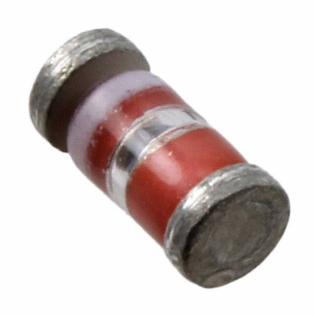
无引脚表面安装,符合DO-213AB(MELF, LL41)封装。

参数特性: - Zener电压范围:6.8伏至110伏。 - 热阻:50°C/W。 - 最大直流功耗:1.0瓦。 - 正向电压@200毫安:1.2伏。

功能详解: - 调节电压,适用于广泛的操作电流和温度范围。 - 低反向(漏)电流。 - 非敏感于静电放电。 - 固有的辐射硬度。

应用信息: - 用于电压调节,特别是在高密度情况下。

封装信息: - 采用MELF(最大外径)封装,具有无铅或RoHS兼容的锡/铅或哑光锡完成的铜包钢端子。 - 标记:阴极带。 - 极性:二极管带带端为正,用于齐纳调节。

电气特性: - 提供了详细的电气特性表,包括标称齐纳电压、齐纳测试电流、最大齐纳阻抗、最大齐纳电流、最大反向漏电流和最大温度系数。

图表: - 提供了温度-功率降额曲线图。

封装尺寸: - 提供了详细的封装尺寸和焊盘布局。
*介绍内容由AI识别生成
JAN1N3017DUR-1/TR 价格&库存

很抱歉,暂时无法提供与“JAN1N3017DUR-1/TR”相匹配的价格&库存,您可以联系我们找货

免费人工找货