0
登录后你可以
  • 下载海量资料
  • 学习在线课程
  • 观看技术视频
  • 写文章/发帖/加入社区
会员中心
创作中心
发布
  • 发文章

  • 发资料

  • 发帖

  • 提问

  • 发视频

创作活动
JAN1N4484D

JAN1N4484D

  • 厂商:

    ACTEL(微芯科技)

  • 封装:

    DO-41

  • 描述:

    DIODE ZENER 62V 1.5W DO41

  • 详情介绍
  • 数据手册
  • 价格&库存
JAN1N4484D 数据手册
1N4460 – 1N4496 and 1N6485 – 1N6491 Available on commercial versions VOIDLESS HERMETICALLY SEALED 1.5 WATT GLASS ZENER DIODES Qualified per MIL-PRF-19500/406 Qualified Levels: JAN, JANTX, JANTXV and JANS DESCRIPTION This Zener voltage regulator series is military qualified to MIL-PRF-19500/406 and is ideal for high-reliability applications where a failure cannot be tolerated. These industry-recognized 1.5 watt Zener voltage regulators are hermetically sealed with void-less glass construction using an internal metallurgical bond. It includes Zener selections from 3.3 to 200 volts in standard 5% tolerance. 1% and 2% tolerance versions are also available. Microsemi also offers numerous other Zener products to meet higher and lower power ratings in both thru-hole and surface mount packages. Important: For the latest information, visit our website http://www.microsemi.com. FEATURES • • • • • • • Popular JEDEC registered series. Void-less hermetically sealed glass package. Triple-layer passivation. Extremely robust construction. Internal “Category 1” metallurgical bonds for 1N4462 thru 1N4496 and “Category III” for 1N6485 thru 1N6491 as well as 1N4460 and 1N4461. JAN, JANTX, JANTXV and JANS qualifications are available per MIL-PRF-19500/406. RoHS compliant versions available (commercial grade only). DO-41 Package Also available in: D-5A MELF Package (surface mount) 1N4460US – 1N4496US and 1N6485US – 1N6491US APPLICATIONS / BENEFITS • • • • • • • Regulates voltage over a broad operating current and temperature range. Extensive selection from 3.3 to 200 V. Standard voltage tolerances are plus/minus 5% with no suffix. Tighter tolerances available in plus or minus 2% or 1%. Flexible axial-lead mounting terminals. Non-sensitive to ESD per MIL-STD-750 method 1020. Inherently radiation hard as described in Microsemi MicroNote 050. o MAXIMUM RATINGS @ T A = 25 C unless otherwise specified Parameters/Test Conditions Junction and Storage Temperature Steady State Power Dissipation @ T L = +112 ºC L = .375 inch (9.53 mm) Thermal Resistance Junction-to-Lead @ .375 inch (9.52 mm) from body 1N4462 – 1N4496 Thermal Impedance @ 10 ms 1N6485 – 1N6491 1N4460 – 1N4461 Forward Voltage @ 200 mA @ 1.0 A Solder Temperature @ 10 s Symbol Value T J & T STG PD -65 to +175 1.5 R ӨJL 42 Z ӨJX Figure 3 Figure 4 Figure 4 1.0 1.5 260 VF T SP Unit o C W o C/W ºC/W V o C MSC – Lawrence 6 Lake Street, Lawrence, MA 01841 Tel: 1-800-446-1158 or (978) 620-2600 Fax: (978) 689-0803 MSC – Ireland Gort Road Business Park, Ennis, Co. Clare, Ireland Tel: +353 (0) 65 6840044 Fax: +353 (0) 65 6822298 Website: www.microsemi.com T4-LDS-0183, Rev. 3 (120901) ©2012 Microsemi Corporation Page 1 of 6 1N4460 – 1N4496 and 1N6485 – 1N6491 MECHANICAL and PACKAGING • • • • • • • CASE: Hermetically sealed voidless hard glass with tungsten slugs. TERMINALS: Tin/lead (Sn/Pb) or RoHS compliant matte/tin (commercial grade only) over copper. MARKING: Body coated in blue with part number. POLARITY: Cathode indicated by band. TAPE & REEL option: Standard per EIA-296. Consult factory for quantities. WEIGHT: 340 milligrams. See Package Dimensions on last page. PART NOMENCLATURE JAN 1N4460 C (e3) Reliability Level JAN = JAN Level JANTX = JANTX Level JANTXV = JANTXV Level JANS = JANS Level Blank = Commercial RoHS Compliance e3 = RoHS compliant (available on commercial grade only) Blank = non-RoHS compliant Tolerance Level Blank = 5 % C=2% D = 1% JEDEC type number (See Electrical Characteristics table) SYMBOLS & DEFINITIONS Definition Symbol VZ I Z , I ZT , I ZK Z ZT or Z ZK VF IR I ZM I ZSM Zener Voltage: The Zener voltage the device will exhibit at a specified current (I Z ) in its breakdown region. Regulator Current: The dc regulator current (I Z ), at a specified test point (I ZT ), near breakdown knee (I ZK ). Dynamic Impedance: The small signal impedance of the diode when biased to operate in its breakdown region at a specified rms current modulation (typically 10% of I ZT or I ZK ) and superimposed on I ZT or I ZK respectively. Maximum Forward Voltage: The maximum forward voltage the device will exhibit at a specified current. Maximum Reverse Current: The maximum reverse (leakage) current that will flow at the specified voltage and temperature. Maximum Regulator (Zener) Current: The maximum rated dc current for the specified power rating. Maximum Zener Surge Current: The non-repetitive peak value of Zener surge current at a specified wave form. T4-LDS-0183, Rev. 3 (120901) ©2012 Microsemi Corporation Page 2 of 6 1N4460 – 1N4496 and 1N6485 – 1N6491 ELECTRICAL CHARACTERISTICS @ 25 ºC Case temperature TYPE NOMINAL ZENER VOLTAGE VZ 1N4460 1N4461 1N4462 1N4463 1N4464 1N4465 1N4466 1N4467 1N4468 1N4469 1N4470 1N4471 1N4472 1N4473 1N4474 1N4475 1N4476 1N4477 1N4478 1N4479 1N4480 1N4481 1N4482 1N4483 1N4484 1N4485 1N4486 1N4487 1N4488 1N4489 1N4490 1N4491 1N4492 1N4493 1N4494 1N4495 1N4496 1N6485 1N6486 1N6487 1N6488 1N6489 1N6490 1N6491 Volts 6.2 6.8 7.5 8.2 9.1 10.0 11.0 12.0 13.0 15.0 16.0 18.0 20.0 22.0 24.0 27.0 30.0 33.0 36.0 39.0 43.0 47.0 51.0 56.0 62.0 68.0 75.0 82.0 91.0 100.0 110.0 120.0 130.0 150.0 160.0 180.0 200.0 3.3 3.6 3.9 4.3 4.7 5.1 5.6 NOTE: TEST MAXIMUM CURRENT DYNAMIC IMPEDANCE I ZT Z ZT @ I ZT mA 40.0 37.0 34.0 31.0 28.0 25.0 23.0 21.0 19.0 17.0 15.5 14.0 12.5 11.5 10.5 9.5 8.5 7.5 7.0 6.5 6.0 5.5 5.0 4.5 4.0 3.7 3.3 3.0 2.8 2.5 2.3 2.0 1.9 1.7 1.6 1.4 1.2 76.0 69.0 64.0 58.0 53.0 49.0 45.0 Ohms 4 2.5 2.5 3 4 5 6 7 8 9 10 11 12 14 16 18 20 25 27 30 40 50 60 70 80 100 130 160 200 250 300 400 500 700 1000 1300 1500 10 10 9 9 8 7 5 MAXIMUM KNEE IMPEDANCE Z ZK @ I ZK Ohms 200 200 400 400 500 500 550 550 550 600 600 650 650 650 700 700 750 800 850 900 950 1000 1100 1300 1500 1700 2000 2500 3000 3100 4000 4500 5000 6000 6500 7000 8000 400 400 400 400 500 500 600 mA 1.0 1.0 .5 .5 .5 .25 .25 .25 .25 .25 .25 .25 .25 .25 .25 .25 .25 .25 .25 .25 .25 .25 .25 .25 .25 .25 .25 .25 .25 .25 .25 .25 .25 .25 .25 .25 .25 1.0 1.0 1.0 1.0 1.0 1.0 1.0 MAXIMUM REVERSE CURRENT IR @ VR µA 10.0 5.0 1.0 .50 .30 .30 .30 .20 .05 .05 .05 .05 .05 .05 .05 .05 .05 .05 .05 .05 .05 .05 .05 .25 .25 .25 .25 .25 .25 .25 .25 .25 .25 .25 .25 .25 .25 50 50 35 5.0 4.0 1.0 0.5 Volts 3.72 4.08 4.50 4.92 5.46 8.00 8.80 9.60 10.4 12.0 12.8 14.4 16.0 17.6 19.2 21.6 24.0 26.4 28.8 31.2 34.4 37.6 40.8 44.8 49.6 54.4 60.0 65.6 72.8 80.0 88.0 96.0 104.0 120.0 128.0 144.0 160.0 1.0 1.0 1.0 1.0 1.0 1.0 2.0 MAXIMUM CONTINUOUS CURRENT I ZM (Note 1) mA 230 210 191 174 157 143 130 119 110 95 90 79 71 65 60 53 48 43 40 37 33 30 28 26 23 21 19 17 16 14 13 12 11 9.5 8.9 7.9 7.2 433 397 366 332 304 280 255 SURGE CURRENT @ 8.3 ms square wave I ZSM Amps 2.3 2.1 1.9 1.7 1.6 1.4 1.3 1.2 1.1 .95 .90 .79 .71 .65 .60 .53 .48 .43 .40 .37 .33 .30 .28 .26 .23 .21 .19 .17 .16 .14 .13 .12 .11 .095 .089 .079 .072 4.2 3.9 3.6 3.3 3.0 2.7 2.5 1. See “Maximum Ratings” for P D temperature conditions for leaded package where I ZM is applicable. T4-LDS-0183, Rev. 3 (120901) ©2012 Microsemi Corporation Page 3 of 6 1N4460 – 1N4496 and 1N6485 – 1N6491 ZENER VOLTAGE GRAPHS TEMPERATURE COEFFICIENT (%/°C) DC Operation Maximum Rating (W) FIGURE 1 Temperature Coefficient Characteristics T L (°C) (Leads) FIGURE 2 Temperature-Power Derating Curve T4-LDS-0183, Rev. 3 (120901) ©2012 Microsemi Corporation Page 4 of 6 1N4460 – 1N4496 and 1N6485 – 1N6491 ZθJX-(°C/W) GRAPHS (continued) t H (Heating time) ms ZθJX-(°C/W) FIGURE 3 Thermal Impedance Curve for 1N4462 through 1N4496 t H (Heating time) ms FIGURE 4 Thermal Impedance Curve for 1N6485 through 1N6491 and 1N4460 through 1N4461 T4-LDS-0183, Rev. 3 (120901) ©2012 Microsemi Corporation Page 5 of 6 1N4460 – 1N4496 and 1N6485 – 1N6491 PACKAGE DIMENSIONS NOTES: 1. Dimensions are in inches. 2. Millimeters are given for general information only. 3. Package contour optional with BD and length BL. Heat slugs, if any, shall be included within this cylinder length but shall not be subject to minimum limit of BD. 4. The specified lead diameters apply in the zone between .050 inch (1.27 mm) from the diode body and the end of the lead. 5. In accordance with ASME Y14.5M, diameters are equivalent to Φx symbology. T4-LDS-0183, Rev. 3 (120901) ©2012 Microsemi Corporation Ltr BD BL LD LL LU DIMENSIONS INCH MILLIMETERS Min Max Min Max .060 .085 1.52 2.16 .106 .160 2.69 4.06 .028 .032 0.71 0.81 .800 1.300 20.32 33.02 .050 1.27 Notes 3 3 4 Page 6 of 6
JAN1N4484D AI解析
物料型号:1N4460至1N4496和1N6485至1N6491

器件简介:这些齐纳二极管是军用级别,符合MIL-PRF-19500/406标准,适用于高可靠性应用,如不能容忍故障的情况。它们采用无空洞的玻璃封装和内部冶金键合,提供从3.3到200伏的齐纳电压选择。

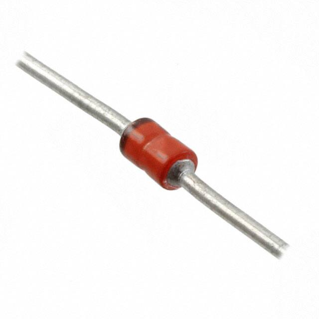
引脚分配:文档中没有明确说明引脚分配,但通常这类二极管会有阳极和阴极两个引脚。

参数特性: - 工作温度范围:-65°C 至 +175°C - 稳态功率耗散:1.5瓦特(在+112°C时) - 热阻:42°C/W(从结到引脚,0.375英寸长度) - 正向电压:在200mA和1.0A测试条件下分别为1.0V和1.5V - 焊接温度:260°C,持续10秒

功能详解:这些齐纳二极管能够在广泛的工作电流和温度范围内调节电压,具有从3.3V到200V的广泛电压选择,标准电压公差为±5%,也提供±2%或±1%的更严格公差版本。

应用信息:它们用于电压调节,具有广泛的电压选择和灵活的轴向引脚安装终端,对静电放电不敏感,并具有固有的辐射硬度。

封装信息:提供DO-41封装和D-5A MELF(表面贴装)封装。封装为真空密封的硬质玻璃,带有钨塞。标记为蓝色,型号号印在外壳上,阳极由带子指示。提供符合RoHS标准的版本(仅限商业等级)。

可靠性等级:包括JAN、JANTX、JANTXV和JANS等级,以及商业等级。

电气特性:在25°C下,提供了包括标称齐纳电压、测试电流、最大动态阻抗、最大膝部阻抗、最大反向电流、最大连续电流和8.3ms方波的浪涌电流等参数。

图表:提供了温度系数特性图、温度-功率降额曲线和热阻曲线。

包装尺寸:详细列出了封装的尺寸,包括直径、长度等。
*介绍内容由AI识别生成
JAN1N4484D 价格&库存

很抱歉,暂时无法提供与“JAN1N4484D”相匹配的价格&库存,您可以联系我们找货

免费人工找货