2N2944A – 2N2946A
PNP Silicon Small Signal Transistor
Available on
commercial
versions
Qualified per MIL-PRF-19500/382
Qualified Levels:
JAN, JANTX, and
JANTXV
DESCRIPTION
This 2N2944A through 2N2946A PNP silicon transistor device is military qualified up to a
JANTXV level for high-reliability applications. Microsemi also offers numerous other products
to meet higher and lower power voltage regulation applications.
Important: For the latest information, visit our website http://www.microsemi.com.
FEATURES
•
JEDEC registered 2N2944A thru 2N2946A series.
•
JAN, JANTX, and JANTXV qualifications per MIL-PRF-19500/382 available.
•
RoHS compliant versions available (commercial grade only).
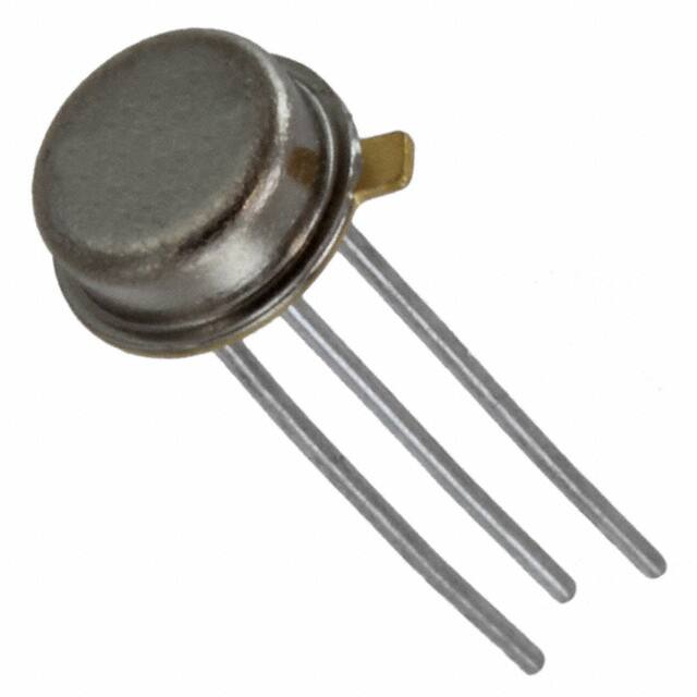
TO-46 (TO-206AB)
Package
APPLICATIONS / BENEFITS
•
•
Also available in:
Low profile metal can package.
ESD to Class 3 per MIL-STD-750, method 1020.
UB package
(surface mount)
2N2944AUB – 2N2946AUB
o
MAXIMUM RATINGS @ +25 C unless specified otherwise.
Parameters/Test Conditions
Junction and Storage Temperature
Thermal Resistance Junction-to-Ambient
Collector Current (dc)
Emitter to Base voltage (static),
collector open
2N2944A
2N2945A
2N2946A
Collector to Base voltage (static),
2N2944A
emitter open
2N2945A
2N2946A
Collector to Emitter voltage (static),
2N2944A
base open
2N2945A
2N2946A
Emitter to Collector voltage
2N2944A
2N2945A
2N2946A
o
(1)
Total Power Dissipation, all terminals @ T A = +25 C
o
Symbol
Value
T J and T STG
R ӨJA
IC
V EBO
-65 to +200
435
-100
-15
-25
-40
-15
-25
-40
-10
-20
-35
-10
-20
-35
400
V CBO
V CEO
V ECO
PT
o
Notes: 1. Derate linearly 2.30 mW / C above T A = +25 C.
Unit
o
o
C
C/W
mA
V
V
V
MSC – Lawrence
6 Lake Street,
Lawrence, MA 01841
Tel: 1-800-446-1158 or
(978) 620-2600
Fax: (978) 689-0803
V
mW
MSC – Ireland
Gort Road Business Park,
Ennis, Co. Clare, Ireland
Tel: +353 (0) 65 6840044
Fax: +353 (0) 65 6822298
Website:
www.microsemi.com
T4-LDS-0236, Rev. 1 (11960)
©2011 Microsemi Corporation
Page 1 of 5
�2N2944A – 2N2946A
MECHANICAL and PACKAGING
•
•
•
•
•
CASE: Nickel plated kovar, glass seals.
TERMINALS: Gold plating over nickel, solder dipped, kovar.
MARKING: Part number, date code, manufacturer’s ID.
WEIGHT: 0.234 grams.
See Package Dimensions on last page.
PART NOMENCLATURE
JAN
2N2944A (e3)
Reliability Level
JAN = JAN Level
JANTX = JANTX Level
JANTXV = JANTXV Level
Blank = Commercial
RoHS Compliance
e3 = RoHS Compliant (available
on commercial grade only)
Blank = non-RoHS Compliant
JEDEC type number
(see Electrical Characteristics
table)
SYMBOLS & DEFINITIONS
Definition
Symbol
IB
IE
V CB
V EB
V (BR)
Base current (dc).
Emitter current (dc).
Collector to base voltage (dc).
Emitter to base voltage (dc).
Minimum Breakdown Voltage: The minimum voltage the device will exhibit at a specified current.
T4-LDS-0236, Rev. 1 (11960)
©2011 Microsemi Corporation
Page 2 of 5
�2N2944A – 2N2946A
o
ELECTRICAL CHARACTERISTICS @ 25 C unless otherwise noted.
Characteristic
Symbol
Min.
Max.
Unit
OFF CHARACTERISTICS:
Collector-Emitter Breakdown Voltage
IC = -10 µA
2N2944A
2N2945A
2N2946A
V(BR)CEO
-10
-20
-35
V
2N2944A
2N2945A
2N2946A
V(BR)ECO
-10
-20
-35
V
Collector-Base Cutoff Current
VCB = -15 V
VCB = -25 V
VCB = -40 V
2N2944A
2N2945A
2N2946A
ICBO
10
10
10
µA
Emitter-Base Cutoff Current
VEB = -12 V
VEB = -20 V
VEB = -32 V
2N2944A
2N2945A
2N2946A
IEBO
2N2944A
2N2945A
2N2946A
Forward-Current Transfer Ratio (inverted connection)
2N2944A
IE = -200 µA, VEC = -0.5 V
2N2945A
2N2946A
Emitter-Collector Offset Voltage
IB = -200 µA, IE = 0
2N2944A
2N2945A
2N2946A
2N2944A
IB = -1.0 mA, IE = 0
2N2945A
2N2946A
2N2944A
IB = -2.0 mA, IE = 0
2N2945A
2N2946A
hFE
100
70
50
hFE(inv)
50
30
20
Emitter-Collector Breakdown Voltage
IE = -10 µA, I B = 0
-0.1
-0.2
-0.5
ηA
VEC(ofs)
-0.3
-0.5
-0.8
-0.6
-1.0
-2.0
-1.0
-1.6
-2.5
mV
2N2944A
2N2945A
2N2946A
2N2944A
2N2945A
2N2946A
rec(on)
10
12
14
4.0
6.0
8.0
2N2944A
2N2945A
2N2946A
|hfe|
ON CHARACTERISTICS: (1)
Forward-Current Transfer Ratio
IC = -1.0 mA, VCE = -0.5 V
DYNAMIC CHARACTERISTICS:
Emitter-Collector On-State Resistance
IB = -100 µA, IE = 0, Ie = 100 µA ac (rms)
f = 1.0 kHz
IB = -1.0 mA, IE = 0, Ie = 100 µA ac (rms)
f =1.0 kHz
Magnitude of Small-Signal Forward
Current Transfer Ratio
IC = -1.0 mA, VCE = -6.0V, f = 1.0 MHz
Output Capacitance
VCB = -6.0 V, IE = 0, 100 kHz ≤ f ≤ 1.0 MHz
Input Capacitance
VEB = -6.0 V, IC = 0, 100 kHz ≤ f ≤ 1.0 MHz
15
10
5.0
Ω
55
55
55
Cobo
10
pF
Cibo
6.0
pF
(1) Pulse Test: Pulse Width = 300 s, duty cycle 2.0%.
T4-LDS-0236, Rev. 1 (11960)
©2011 Microsemi Corporation
Page 3 of 5
�2N2944A – 2N2946A
Maximum DC Operation Rating (mW )
GRAPHS
o
T A ( C) Ambient Temperature
FIGURE 1 – Temperature-Power Derating Curve
T4-LDS-0236, Rev. 1 (11960)
©2011 Microsemi Corporation
Page 4 of 5
�2N2944A – 2N2946A
PACKAGE DIMENSIONS
Ltr.
CD
CH
HD
LC
LD
LL
LU
L1
L2
Q
TL
TW
r
α
Dimensions
Inches
Millimeters
Min
Max
Min
Max
.178
.195
4.52
4.95
.065
.085
1.65
2.16
.209
.230
5.31
5.84
.100 TP
2.54 TP
.016
.021
0.41
0.53
.500
1.750
12.70 44.45
.016
.019
0.41
0.48
.050
1.27
.250
6.35
.040
1.02
.028
.048
0.71
1.22
.036
.046
0.91
1.17
.010
0.25
45° TP
45° TP
Notes
5
6
6
6
6
3
8
4
9
5
NOTES:
1. Dimensions are in inches.
2. Millimeters are given for general information only.
3. Symbol TL is measured from HD maximum.
4. Details of outline in this zone are optional.
5. Leads at gauge plane .054 inch (1.37 mm) +.001 inch (0.03 mm) -.000 inch (0.00 mm) below seating plane shall be within
.007 inch (0.18 mm) radius of TP relative to tab. Device may be measured by direct methods or by gauge.
6. Symbol LU applies between L1 and L2. Dimension LD applies between L2 and LL minimum.
7. Lead number three is electrically connected to case.
8. Beyond r maximum, TW shall be held for a minimum length of .011 inch (0.28 mm).
9. Symbol r applied to both inside corners of tab.
10. In accordance with ASME Y14.5M, diameters are equivalent to Φx symbology.
11. Lead 1 is emitter, lead 2 is base, and lead 3 is collector.
T4-LDS-0236, Rev. 1 (11960)
©2011 Microsemi Corporation
Page 5 of 5
�