2N2904AL and 2N2905AL
Qualified Levels:
JAN, JANTX, JANTXV
and JANS
PNP SWITCHING SILICON
TRANSISTOR
Available on
commercial
versions
Qualified per MIL-PRF-19500/290
DESCRIPTION
This family of 2N2904AL and 2N2905AL switching transistors are military qualified up to the
JANS level for high-reliability applications. These devices are also available in a TO-39
package. Microsemi also offers numerous other transistor products to meet higher and lower
power ratings with various switching speed requirements in both through-hole and surfacemount packages.
Important: For the latest information, visit our website http://www.microsemi.com.
FEATURES
•
JEDEC registered 2N2904 through 2N2905 series.
•
JAN, JANTX, JANTXV, and JANS qualifications are available per MIL-PRF-19500/290.
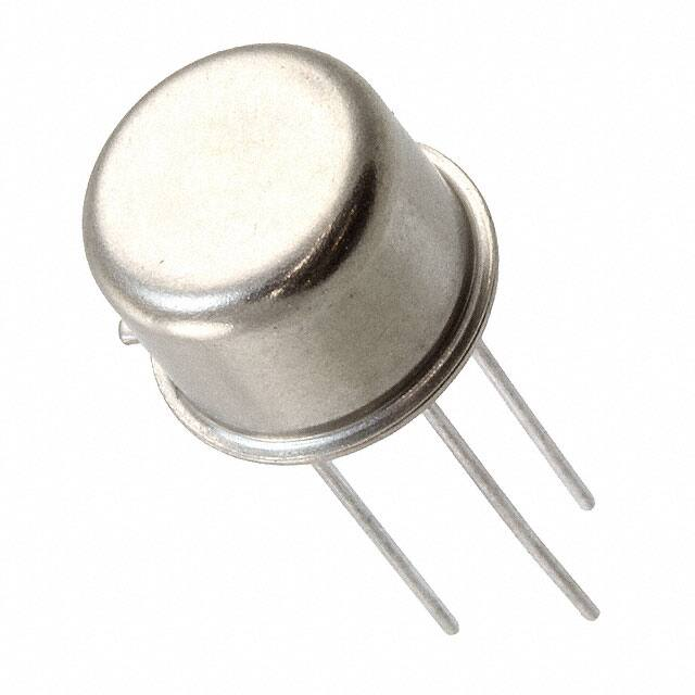
TO-5 Package
(See part nomenclature for all available options.)
•
RoHS compliant versions available (commercial grade only).
Also available in:
TO-39 (TO-205AD)
package
(long-leaded)
2N2904 & 2N2905A
APPLICATIONS / BENEFITS
•
•
General purpose transistors for high speed switching applications.
Military and other high-reliability applications.
MAXIMUM RATINGS
Parameters / Test Conditions
Symbol
Value
Unit
Collector-Emitter Voltage
VCEO
60
V
Collector-Base Voltage
VCBO
60
V
Emitter-Base Voltage
VEBO
5.0
V
Thermal Resistance Junction-to-Ambient
RӨJA
195
o
Thermal Resistance Junction-to-Case
RӨJC
50
o
IC
600
mA
PT
0.8
3.0
W
TJ and Tstg
-65 to +200
°C
Collector Current
Total Power Dissipation
(1)
@ TA = +25 °C
@ TC = +25 °C (2)
Operating & Storage Junction Temperature Range
Notes: 1. For derating, see figures 1 and 2.
2. For thermal impedance, see figures 3 and 4.
C/W
C/W
MSC – Lawrence
6 Lake Street,
Lawrence, MA 01841
Tel: 1-800-446-1158 or
(978) 620-2600
Fax: (978) 689-0803
MSC – Ireland
Gort Road Business Park,
Ennis, Co. Clare, Ireland
Tel: +353 (0) 65 6840044
Fax: +353 (0) 65 6822298
Website:
www.microsemi.com
T4-LDS-0186-1, Rev. 1 (121219)
©2012 Microsemi Corporation
Page 1 of 7
�2N2904AL and 2N2905AL
MECHANICAL and PACKAGING
•
•
•
•
•
•
CASE: Hermetically sealed, kovar base, nickel cap.
TERMINALS: Tin/lead plate or RoHS compliant matte/tin (commercial grade only) over nickel.
MARKING: Part number, date code, manufacturer’s ID.
POLARITY: PNP (see package outline).
WEIGHT: Approximately 1.14 grams.
See Package Dimensions on last page.
PART NOMENCLATURE
JAN
2N2904
A
L
(e3)
Reliability Level
JAN = JAN Level
JANTX = JANTX Level
JANTXV = JANTXV Level
JANS = JANS Level
Blank = Commercial
RoHS Compliance
e3 = RoHS compliant (available
on commercial grade only)
Blank = non-RoHS compliant
JEDEC type number
(see Electrical Characteristics
table)
Electrical Parameter Modifier
Symbol
Cobo
ICEO
ICEX
IEBO
hFE
VCEO
VCBO
VEBO
Long Leaded
SYMBOLS & DEFINITIONS
Definition
Common-base open-circuit output capacitance.
Collector cutoff current, base open.
Collector cutoff current, circuit between base and emitter.
Emitter cutoff current, collector open.
Common-emitter static forward current transfer ratio.
Collector-emitter voltage, base open.
Collector-emitter voltage, emitter open.
Emitter-base voltage, collector open.
T4-LDS-0186-1, Rev. 1 (121219)
©2012 Microsemi Corporation
Page 2 of 7
�2N2904AL and 2N2905AL
ELECTRICAL CHARACTERISTICS @ TA = +25 °C, unless otherwise noted
Parameters / Test Conditions
OFF CHARACTERISTICS
Collector-Emitter Breakdown Current
IC = 10 mA
Symbol
Min.
V(BR)CEO
60
Max.
Unit
V
Collector-Emitter Cutoff Voltage
VCE = 60 V
ICES
1.0
µA
Collector-Base Cutoff Current
VCB = 60 V
All Types
ICBO1
10
µA
VCB = 50 V
2N2904AL, 2N2905AL
ICBO2
10
nA
VCB = 50 V @ TA = +150 ºC 2N2904AL, 2N2905AL
ICBO3
10
µA
Collector-Base Cutoff Current
VCB = 50 V
ICBO
10
nA
10
µA
50
10
nA
µA
VCB = 60 V
Emitter-Base Cutoff Current
VEB = 3.5 V
VEB = 5.0 V
IEBO
ON CHARACTERISTICS (1)
Forward-Current Transfer Ratio
IC = 0.1 mA, VCE = 10 V
2N2904AL
2N2905AL
40
75
IC = 1.0 mA, VCE = 10 V
2N2904AL
2N2905AL
40
100
IC = 10 mA, VCE = 10 V
2N2904AL
2N2905AL
IC = 150 mA, VCE = 10 V
2N2904AL
2N2905AL
40
100
IC = 500 mA, VCE = 10 V
2N2904AL
2N2905AL
40
50
hFE
175
450
40
100
120
300
Collector-Emitter Saturation Voltage
IC = 150 mA, IB = 15 mA
IC = 500 mA, IB = 50 mA
VCE(sat)
0.4
1.6
V
Base-Emitter Saturation Voltage
IC = 150 mA, IB = 15 mA
IC = 500 mA, IB = 50 mA
VBE(sat)
1.3
2.6
V
(1) Pulse Test: Pulse Width = 300 µs, duty cycle ≤ 2.0%.
T4-LDS-0186-1, Rev. 1 (121219)
©2012 Microsemi Corporation
Page 3 of 7
�2N2904AL and 2N2905AL
ELECTRICAL CHARACTERISTICS @ TA = +25 °C, unless otherwise noted (continued)
DYNAMIC CHARACTERISTICS
Parameters / Test Conditions
Small-Signal Short-Circuit Forward-Current
Transfer Ratio
IC = 1.0 mA, VCE = 10 V, f = 1.0 kHz
Small-Signal Short-Circuit Forward-Current
Transfer Ratio
IC = 50 mA, VCE = 20 V, f = 100 MHz
Output Capacitance
VCB = 10 V, IE = 0, 100 kHz ≤ f ≤ 1.0MHz
Iutput Capacitance
VEB = 2.0 V, IC = 0, 100 kHz ≤ f ≤ 1.0MHz
Symbol
Min.
Max.
hfe
100
|hfe|
2.0
Cobo
8.0
Cibo
30
Unit
pF
pF
SWITCHING CHARACTERISTICS
Parameters / Test Conditions
Symbol
Turn-On Time
t
Turn-Off Time
t
T4-LDS-0186-1, Rev. 1 (121219)
Max.
Unit
on
45
ns
off
300
ns
©2012 Microsemi Corporation
Min.
Page 4 of 7
�2N2904AL and 2N2905AL
DC Operation Maximum Rating (W)
GRAPHS
Ta (°C) (Ambient)
DC Operation Maximum Rating (W)
FIGURE 1
Derating (RθJA) PCB
Tc (ºC) (Case)
FIGURE 2
Derating (RθJA) PCB
T4-LDS-0186-1, Rev. 1 (121219)
©2012 Microsemi Corporation
Page 5 of 7
�2N2904AL and 2N2905AL
Theta (oC/W)
GRAPHS (continued)
Time (s)
FIGURE 3
Theta (oC /W)
Thermal impedance graph (RθJA)
Time (s)
FIGURE 4
Thermal impedance graph (RθJA)
T4-LDS-0186-1, Rev. 1 (121219)
©2012 Microsemi Corporation
Page 6 of 7
�2N2904AL and 2N2905AL
PACKAGE DIMENSIONS
CD
CH
HD
LC
Dimensions
Millimeters
Min
Max
Min
Max
0.305
0.335
7.75
8.51
0.240
0.260
6.10
6.60
0.335
0.370
8.51
9.40
0.200 TP
5.08 TP
LD
0.016
0.021
0.41
0.53
7, 8
LL
LU
0.500
0.016
0.750
0.019
12.70
0.41
19.05
0.48
7, 8, 12
7, 8
1.27
7, 8
Symbol
Inch
L1
0.050
L2
0.250
6.35
P
Q
TL
TW
r
α
0.100
2.54
0.050
0.029
0.045
0.028
0.034
0.010
45° TP
1.27
0.74
1.14
0.71
0.86
0.25
45° TP
Note
6
7, 8
5
4
3
10
6
NOTES:
1.
2.
3.
4.
5.
6.
7.
8.
9.
10.
11.
12.
13.
Dimensions are in inches.
Millimeters are given for general information only.
Beyond r (radius) maximum, TW shall be held for a minimum length of .011 (0.28 mm).
Dimension TL measured from maximum HD.
Body contour optional within zone defined by HD, CD, and Q.
Leads at gauge plane .054 +.001 -.000 inch (1.37 +0.03 -0.00 mm) below seating plane shall be within .007 inch
(0.18 mm) radius of true position (TP) at maximum material condition (MMC) relative to tab at MMC.
Dimension LU applies between L1 and L2. Dimension LD applies between L2 and LL minimum. Diameter is
uncontrolled in L1 and beyond LL minimum.
All three leads.
The collector shall be internally connected to the case.
Dimension r (radius) applies to both inside corners of tab.
In accordance with ASME Y14.5M, diameters are equivalent to Φx symbology.
For “L” suffix devices, dimension LL is 1.50 (38.10 mm) minimum, 1.75 (44.45 mm) maximum.
Lead 1 = emitter, lead 2 = base, lead 3 = collector.
T4-LDS-0186-1, Rev. 1 (121219)
©2012 Microsemi Corporation
Page 7 of 7
�