TECHNICAL DATA SHEET
6 Lake Street, Lawrence, MA 01841
1-800-446-1158 / (978) 620-2600 / Fax: (978) 689-0803
Website: http://www.microsemi.com
NPN POWER SILICON TRANSISTOR
Qualified per MIL-PRF-19500/514
DEVICES
LEVELS
2N6274
2N6277
JAN
JANTX
JANTXV
ABSOLUTE MAXIMUM RATINGS (TC = +25°C unless otherwise noted)
Parameters / Test Condition
Symbol
2N6274
2N6277
Unit
Collector-Emitter Voltage
VCEO
100
150
Vdc
Collector-Base Voltage
VCBO
120
180
Vdc
Emitter-Base Voltage
VEBO
6.0
6.0
Vdc
Base Current
IB
20
20
Adc
Collector Current
IC
50
50
250
143
-65 to +200
Adc
@ TC = +25°C (1)
Total Power Dissipation
@ TC = +100°C (2)
Operating & Storage Temperature Range
PT
Tj , Tstg
W
°C
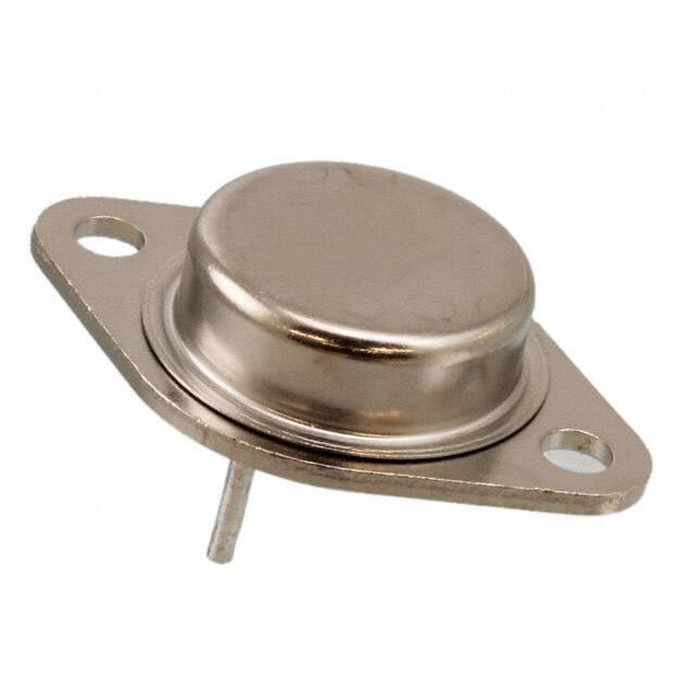
TO-3 (TO-204AE)
THERMAL CHARACTERISTICS
Parameters / Test Conditions
Thermal resistance, Junction-to-Case
Symbol
Max
Unit
RθJC
0.7
°C/W
Note: 1) Derate linearly 1.43 W/°C between TC = +25°C and TC = 200°C
ELECTRICAL CHARACTERISTICS (TA = +25°C, unless otherwise noted)
Parameters / Test Conditions
Symbol
Min.
Max.
Unit
2N6274
2N6277
V(BR)CEO
100
150
2N6274
2N6277
ICEO
50
50
µAdc
2N6274
2N6277
ICEX
10
10
µAdc
2N6274
2N6277
ICBO
10
10
µAdc
IEBO
100
µAdc
OFF CHARACTERTICS (1)
Collector-Emitter Breakdown Voltage
IC = 50mAdc
Collector-Emitter Cutoff Current
VCE = 50Vdc
VCE = 75Vdc
Collector-Emitter Cutoff Current
VCE = 120Vdc, VBE = -1.5Vdc
VCE = 180Vdc, VBE = -1.5Vdc
Collector-Base Cutoff Current
VCB = 120Vdc
VCB = 180Vdc
Emitter-Base Cutoff Current
VEB = 6.0Vdc
T4-LDS-0163 Rev. 1 (100546)
Vdc
Page 1 of 3
�TECHNICAL DATA SHEET
6 Lake Street, Lawrence, MA 01841
1-800-446-1158 / (978) 620-2600 / Fax: (978) 689-0803
Website: http://www.microsemi.com
ELECTRICAL CHARACTERISTICS (TA = +25°C, unless otherwise noted)
Parameters / Test Conditions
Symbol
Min.
Max.
hFE
50
30
10
120
Unit
(2)
ON CHARACTERISTICS
Forward-Current Transfer Ratio
IC = 1.0Adc, VCE = 4.0Vdc
IC = 20Adc, VCE = 4.0Vdc
IC = 50Adc, VCE = 4.0Vdc
Collector-Emitter Saturation Voltage
IC = 20Adc, IB = 2.0Adc
IC = 50Adc, IB = 10Adc
Base-Emitter Saturation Voltage
IC = 20Adc, IB = 2.0Adc
VCE(sat)
1.0
3.0
Vdc
VBE(sat)
1.8
Vdc
Min.
Max.
Unit
3.0
12
DYNAMIC CHARACTERISTICS
Parameters / Test Conditions
Magnitude of Common Emitter Small-Signal Short-Circuit, Forward
Current Transfer Ratio
IC = 1.0Adc, VCE = 10Vdc, f = 10MHz
Output Capacitance
VCB = 10Vdc, IE = 0, f = 1.0MHz
Symbol
|hfe|
Cobo
600
pF
Max.
Unit
SWITCHING CHARACTERISTICS
Parameters / Test Conditions
Symbol
Min.
Turn-On Time
VCC = 80Vdc; IC = 20Adc; IB = 2.0Adc
ton
0.5
μs
Turn-Off Time
VCC = 80Vdc ; IC = 20Adc; IB1 = -IB2 = 2.0Adc
toff
1.05
μs
SAFE OPERATING AREA
DC Tests
TC = +25°C, 1 Cycle, t = 1.0s
Test 1
VCE = 5.0Vdc, IC = 50Adc
All Types
Test 2
VCE = 8.6Vdc, IC = 165mAdc
All Types
Test 3
VCE = 80Vdc, IC = 29mAdc
2N6274
Test 4
VCE = 120Vdc, IC = 110mAdc
2N6277
(2) Pulse Test: Pulse Width = 300µs, Duty Cycle ≤ 2.0%
T4-LDS-0163 Rev. 1 (100546)
Page 2 of 3
�TECHNICAL DATA SHEET
6 Lake Street, Lawrence, MA 01841
1-800-446-1158 / (978) 620-2600 / Fax: (978) 689-0803
Website: http://www.microsemi.com
PACKAGE DIMENSIONS
Ltr
CD
CH
HR
HR1
HT
LD
LL
L1
MHD
MHS
PS
PS1
S1
Dimensions
Inches
Millimeters
Min
Max
Min
Max
.875
22.22
.250
.328
6.35
8.33
.495
.525
12.57
13.34
.131
.188
3.33
4.78
.060
.135
1.52
3.43
.057
.063
1.45
1.60
.312
.500
7.92
12.70
.050
1.27
.151
.161
3.84
4.09
1.177
1.197
29.90
30.40
.420
.440
10.67
11.18
.205
.225
5.21
5.72
.655
.675
16.64
17.15
Notes
3
6
5, 9
4, 5, 9
5, 9
7
5
NOTE:
1.
* 2.
3.
4.
*
*
5.
6.
7.
8.
9.
10.
11.
Dimensions are in inches.
Millimeters are given for general information only.
Body contour is optional within zone defined by CD.
These dimensions shall be measured at points .050 inch (1.27 mm) to .055 inch (1.40 mm) below seating plane. When
gauge is not used, measurement shall be made at seating plane.
Both terminals.
At both ends.
Two holes.
Terminal 1 is the emitter, terminal 2 is base. The collector shall be electrically connected to the case.
LD applies between L1 and LL. Lead diameter shall not exceed twice LD within L1.
In accordance with ASME Y14.5M, diameters are equivalent to φx symbology.
The seating plane of the header shall be flat within .001 inch (0.03 mm) concave to .004 inch (0.10 mm) convex inside a
.930 inch (23.62 mm) diameter circle on the center of the header and flat within .001 inch (0.03 mm) concave to .006 inch
(0.15 mm) convex overall.
* FIGURE 1. Physical dimensions (TO-3)
T4-LDS-0163 Rev. 1 (100546)
Page 3 of 3
�
很抱歉,暂时无法提供与“JANTX2N6274”相匹配的价格&库存,您可以联系我们找货
免费人工找货