物料型号:1N4460US至1N4496US和1N6485US至1N6491US
器件简介:这些齐纳二极管是军用级别,符合MIL-PRF-19500/406标准,适用于高可靠性应用,采用无空洞玻璃封装和内部冶金键合。提供从3.3伏到200伏的标准5%容差齐纳电压选择,也提供1%和2%容差版本。
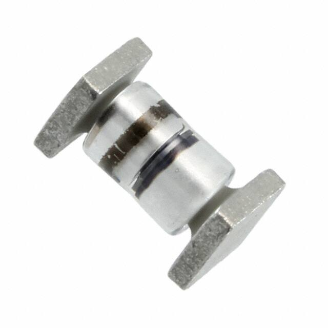
引脚分配:文档中未明确列出引脚分配,但提到了表面安装和MELF封装两种形式。
参数特性:
- 工作温度范围:-65°C至+175°C
- 稳态功率耗散:1.5瓦特
- 热阻(结到端盖):20°C/W
- 正向电压:在200mA和1.0A测试条件下分别为1.0V和1.5V
- 焊接温度:260°C,10秒
功能详解:这些齐纳二极管能够在广泛的工作电流和温度范围内调节电压,具有从3.3V到200V的广泛选择,并且对静电放电不敏感。
应用信息:适用于需要电压调节的场合,具有广泛的电压选择和标准电压容差。
封装信息:包括密封的无空洞硬玻璃封装,带有钨块。端子材料为锡/铅或符合RoHS标准的商业等级的铜上覆盖物。