KSZ8794CNX
Integrated 4-Port 10/100 Managed Ethernet
Switch with Gigabit RGMII/MII/RMII Interface
Target Applications
• Industrial Ethernet Applications that Employ IEEE
802.3-Compliant MACs. (Ethernet/IP, Profinet,
MODBUS TCP, etc.)
• VoIP Phone
• Set-Top/Game Box
• Automotive
• Industrial Control
• IPTV POF
• SOHO Residential Gateway with Full-Wire Speed
of Four LAN Ports
• Broadband Gateway/Firewall/VPN
• Integrated DSL/Cable Modem
• Wireless LAN Access Point + Gateway
• Standalone 10/100 Switch
• Networked Measurement and Control Systems
Features
• Management Capabilities
- The KSZ8794CNX Includes All the Functions
of a 10/100BASE-T/TX Switch System Which
Combines a Switch Engine, Frame Buffer
Management, Address Look-Up Table,
Queue Management, MIB Counters, Media
Access Controllers (MAC), and PHY Transceivers
- Non-Blocking Store-and-Forward Switch
Fabric Assures Fast Packet Delivery by Utilizing a 1024-Entries Forwarding Table
- Port Mirroring/Monitoring/Sniffing: Ingress
and/or Egress Traffic to Any Port
- MIB Counters for Fully Compliant Statistics
Gathering (36 Counters per Port)
- Support Hardware for Port-Based Flush and
Freeze Command in MIB Counter.
- Multiple Loopback of Remote PHY, and MAC
Modes Support for the Diagnostics
- Rapid Spanning Tree Support (RSTP) for
Topology Management and Ring/Linear
Recovery
• Robust PHY Ports
- Four Integrated IEEE 802.3/802.3u-Compliant Ethernet Transceivers Supporting
10BASE-T and 100BASE-TX
- IEEE 802.1az EEE Supported
2016-2020 Microchip Technology Inc.
- On-Chip Termination Resistors and Internal
Biasing for Differential Pairs to Reduce
Power
- HP Auto MDI/MDI-X Crossover Support Eliminates the Need to Differentiate Between
Straight or Crossover Cables in Applications
• MAC and GMAC Ports
- Three Internal Media Access Control (MAC1
to MAC3) Units and One Internal Gigabit
Media Access Control (GMAC4) Unit
- RGMII, MII, or RMII Interfaces Support for
the Port 4 GMAC4 with Uplink
- 2 KByte Jumbo Packet Support
- Tail Tagging Mode (One Byte Added Before
FCS) Support on Port 4 to Inform the Processor in which Ingress Port Receives the
Packet and its Priority
- Supports Reduced Media Independent Interface (RMII) with 50 MHz Reference Clock
Output
- Supports Media Independent Interface (MII)
in Either PHY Mode or MAC Mode on Port 4
- LinkMD® Cable Diagnostic Capabilities for
Determining Cable Opens, Shorts, and
Length
• Advanced Switch Capabilities
- Non-Blocking Store-and-Forward Switch
Fabric Assures Fast Packet Delivery by Utilizing a 1024-Entries Forwarding Table
- 64 KB Frame Buffer RAM
- IEEE 802.1q VLAN Support for up to 128
Active VLAN Groups (Full-Range 4096 of
VLAN IDs)
- IEEE 802.1p/Q Tag Insertion or Removal on
a Per Port Basis (Egress)
- VLAN ID Tag/Untag Options on Per Port
Basis
- Fully Compliant with IEEE 802.3/802.3u
Standards
- IEEE 802.3x Full-Duplex with Force-Mode
Option and Half-Duplex Back-Pressure Collision Flow Control
- IEEE 802.1w Rapid Spanning Tree Protocol
Support
- IGMP v1/v2/v3 Snooping for Multicast Packet
Filtering
DS00002134B-page 1
�KSZ8794CNX
- QoS/CoS Packets Prioritization Support:
802.1p, DiffServ-Based and Re-Mapping of
802.1p Priority Field Per Port Basis on Four
Priority Levels
- IPv4/IPv6 QoS Support
- IPv6 Multicast Listener Discovery (MLD)
Snooping
- Programmable Rate Limiting at the Ingress
and Egress Ports on a Per Port Basis
- Jitter-Free Per Packet Based Rate Limiting
Support
- Tail Tag Mode (1 byte Added before FCS)
Support on Port 4 to Inform the Processor
which Ingress Port Receives the Packet
- Broadcast Storm Protection with Percentage
Control (Global and Per Port Basis)
- 1K Entry Forwarding Table with 64 KB Frame
Buffer
- 4 Priority Queues with Dynamic Packet Mapping for IEEE 802.1P, IPv4 TOS (DIFFSERV), IPv6 Traffic Class, etc.
- Supports WoL Using AMD’s Magic Packet
- VLAN and Address Filtering
- Supports 802.1x Port-Based Security,
Authentication and MAC-Based Authentication via Access Control Lists (ACL)
- Provides Port-Based and Rule-Based ACLs
to Support Layer 2 MAC SA/DA Address,
Layer 3 IP Address and IP Mask, Layer 4
TCP/UDP Port Number, IP Protocol, TCP
Flag and Compensation for the Port Security
Filtering
- Ingress and Egress Rate Limit Based on Bit
per Second (bps) and Packet-Based Rate
Limiting (pps)
• Configuration Registers Access
- High-Speed SPI (4-Wire, up to 50 MHz) Interface to Access All Internal Registers
- MII Management (MIIM, MDC/MDIO 2-Wire)
Interface to Access All PHY Registers per
Clause 22.2.4.5 of the IEEE 802.3 Specification
- I/O Pin Strapping Facility to Set Certain Register Bits from I/O Pins During Reset Time
- Control Registers Configurable On-the-Fly
• Power and Power Management
- Full-Chip Software Power-Down (All Register
Values are Not Saved and Strap-In Value Will
Re-Strap After it Releases the Power-Down)
- Per-Port Software Power-Down
- Energy Detect Power-Down (EDPD), which
Disables the PHY Transceiver When Cables
are Removed
- Supports IEEE P802.3az Energy Efficient
Ethernet (EEE) to Reduce Power Consump-
2016-2020 Microchip Technology Inc.
tion in Transceivers in LPI State Even
Though Cables are Not Removed
- Dynamic Clock Tree Control to Reduce
Clocking in Areas that are Not in Use
- Low Power Consumption without Extra
Power Consumption on Transformers
- Voltages: Using External LDO Power Supplies
- Analog VDDAT 3.3V or 2.5V
- VDDIO Support 3.3V, 2.5V, and 1.8V
- Low 1.2V Voltage for Analog and Digital Core
Power
- WoL Support with Configurable Packet Control
• Additional Features
- Single 25 MHz ±50 ppm Reference Clock
Requirement
- Comprehensive Programmable Two-LED
Indicator Support for Link, Activity, Full-/HalfDuplex, and 10/100 Speed
• Packaging and Environmental
- Commercial Temperature Range: 0°C to
+70°C
- Industrial Temperature Range: –40°C to
+85°C
- Small Package Available in a Lead-Free,
RoHS-Compliant 64-Pin QFN
- 0.065 µm CMOS Technology for Lower
Power Consumption
DS00002134B-page 2
�KSZ8794CNX
TO OUR VALUED CUSTOMERS
It is our intention to provide our valued customers with the best documentation possible to ensure successful use of your Microchip
products. To this end, we will continue to improve our publications to better suit your needs. Our publications will be refined and
enhanced as new volumes and updates are introduced.
If you have any questions or comments regarding this publication, please contact the Marketing Communications Department via
E-mail at docerrors@microchip.com. We welcome your feedback.
Most Current Data Sheet
To obtain the most up-to-date version of this data sheet, please register at our Worldwide Web site at:
http://www.microchip.com
You can determine the version of a data sheet by examining its literature number found on the bottom outside corner of any page.
The last character of the literature number is the version number, (e.g., DS30000000A is version A of document DS30000000).
Errata
An errata sheet, describing minor operational differences from the data sheet and recommended workarounds, may exist for current devices. As device/documentation issues become known to us, we will publish an errata sheet. The errata will specify the
revision of silicon and revision of document to which it applies.
To determine if an errata sheet exists for a particular device, please check with one of the following:
• Microchip’s Worldwide Web site; http://www.microchip.com
• Your local Microchip sales office (see last page)
When contacting a sales office, please specify which device, revision of silicon and data sheet (include -literature number) you are
using.
Customer Notification System
Register on our web site at www.microchip.com to receive the most current information on all of our products.
2016-2020 Microchip Technology Inc.
DS00002134B-page 3
�KSZ8794CNX
Table of Contents
1.0 Introduction ..................................................................................................................................................................................... 5
2.0 Pin Description and Configuration ................................................................................................................................................... 6
3.0 Functional Description ................................................................................................................................................................... 12
4.0 Device Registers ........................................................................................................................................................................... 43
5.0 Operational Characteristics ......................................................................................................................................................... 106
6.0 Electrical Characteristics ............................................................................................................................................................. 107
7.0 Timing Diagrams .......................................................................................................................................................................... 109
8.0 Reset Circuit................................................................................................................................................................................. 117
9.0 Selection of Isolation Transformer ............................................................................................................................................... 118
10.0 Selection of Reference Crystal................................................................................................................................................... 118
11.0 Package Outlines ....................................................................................................................................................................... 119
Appendix A: Data Sheet Revision History ......................................................................................................................................... 120
The Microchip Web Site .................................................................................................................................................................... 121
Customer Change Notification Service ............................................................................................................................................. 121
Customer Support ............................................................................................................................................................................. 121
Product Identification System ............................................................................................................................................................ 122
DS00002134B-page 4
2016-2020 Microchip Technology Inc.
�KSZ8794CNX
1.0
INTRODUCTION
1.1
General Description
The KSZ8794CNX is a highly integrated, Layer 2-managed, four-port switch with numerous features designed to reduce
system cost. It is intended for cost-sensitive applications requiring three 10/100 Mbps copper ports and one 10/100/
1000 Mbps Gigabit uplink port. The KSZ8794CNX incorporates a small package outline, lowest power consumption with
internal biasing, and on-chip termination. Its extensive features set includes enhanced power management, programmable rate limiting and priority ratio, tagged and port-based VLAN, port-based security and ACL rule-based packet filtering technology, QoS priority with four queues, management interfaces, enhanced MIB counters, high-performance
memory bandwidth, and a shared memory-based switch fabric with non-blocking support. The KSZ8794CNX provides
support for multiple CPU data interfaces to effectively address both current and emerging fast Ethernet and Gigabit
Ethernet applications where the GMAC interface can be configured to any of RGMII, MII, and RMII modes. The
KSZ8794CNX is built on the latest industry-leading Ethernet analog and digital technology, with features designed to
offload host processing and streamline the overall design:
• Three integrated 10/100BASE-T/TX MAC/PHYs.
• One integrated 10/100/1000BASE-T/TX GMAC with selectable RGMII, MII, or RMII interfaces.
• Small 64-pin QFN package.
A robust assortment of power management features including Energy Efficient Ethernet (EEE), PME, and WoL have
been designed in to satisfy energy efficient environments.
All registers in the MAC and PHY units can be managed through the SPI interface. MIIM PHY registers can be accessed
through the MDC/MDIO interface.
FIGURE 1-1:
FUNCTIONAL BLOCK DIAGRAM
KSZ8794
10/100
MAC 1
AUTO MDI/MDIX
10/100
T/TX
EEE PHY2
10/100
MAC 2
AUTO MDI/MDIX
10/100
T/TX
EEE PHY3
10/100
MAC 3
10/100/1000
GMAC 4
SW4-RGMII/MII/RMII
MDC, MDI/O FOR MIIM
SPI
CONTROL REG SPI I/F
LED0 {3:1]
LED1 {3:1]
2016-2020 Microchip Technology Inc.
LED I/F
CONTROL
REGISTERS
LOOK UP ENGINE
FIFO, FLOW CONTROL, VLAN TAGGING, PRIORITY
AUTO MDI/MDIX
10/100
T/TX
EEE PHY1
QUEUE MANAGEMENT
BUFFER MANAGEMENT
FRAME BUFFER
MIB COUNTERS
DS00002134B-page 5
�KSZ8794CNX
2.0
PIN DESCRIPTION AND CONFIGURATION
64-QFN PIN ASSIGNMENT (TOP VIEW)
XO
XI
GNDA
ISET
VDDAT33
VDD12D
RST_N
GNDD
VDDIO
SPIS_N
SDA_MDIO
SCL_MDC
SPIQ
LED1_0
LED1_1
LED2_0
FIGURE 2-1:
64 63 62 61 60 59 58 57 56 55 54 53 52 51 50 49
VDD12A
VDDAT33
GNDA
RXP1
RXM1
TXP1
TXM1
RXP2
RXM2
TXP2
TXM2
VDDAT33
RXP3
RXM3
TXP3
TXM3
1
2
3
4
5
6
7
8
9
10
11
12
13
14
15
16
KSZ8794
(Top View)
64-pin QFN
48
47
46
45
44
43
42
41
40
39
38
37
36
35
34
33
LED2_1
PME
REFCLKO
COL4
CRS4
RXER4
RXDV4/CRSDV4/RXD4_CTL
RXD4_3
RXD4_2
VDDIO
GNDD
RXD4_1
RXD4_0
RXC4/GRXC4
TXC4/REFCLKI4/GTXC4
VDD12D
GNDA
INTR_N
LED3_1
LED3_0
VDD12D
GNDD
TXEN4
TXD4_0
TXD4_1
GNDD
VDDIO
TXD4_2
TXD4_3
TXER4
NC
GNDD
17 18 19 20 21 22 23 24 25 26 27 28 29 30 31 32
DS00002134B-page 6
2016-2020 Microchip Technology Inc.
�KSZ8794CNX
TABLE 2-1:
SIGNALS - KSZ8794CNX
Pin
Number
Pin
Name
Type
Note 2-1
Port
1
VDD12A
P
—
1.2V Core Power
2
VDDAT
P
—
3.3V or 2.5V Analog Power.
3
GNDA
GND
—
Analog Ground.
4
RXP1
I
1
Port 1 Physical Receive Signal + (Differential).
5
RXM1
I
1
Port 1 Physical Receive Signal - (Differential).
6
TXP1
O
1
Port 1 Physical Transmit Signal + (Differential).
7
TXM1
O
1
Port 1 Physical Transmit Signal - (Differential).
8
RXP2
I
2
Port 2 Physical Receive Signal + (Differential).
9
RXM2
I
2
Port 2 Physical Receive Signal - (Differential).
10
TXP2
O
2
Port 2 Physical Transmit Signal + (Differential).
11
TXM2
O
2
Port 2 Physical Transmit Signal - (Differential).
12
VDDAT
P
—
3.3V or 2.5V Analog Power.
13
RXP3
I
3
Port 3 Physical Receive Signal + (Differential).
14
RXM3
I
3
Port 3 Physical Receive Signal - (Differential).
15
TXP3
O
3
Port 3 Physical Transmit Signal + (Differential).
16
TXM3
O
3
Port 3 Physical Transmit Signal – (Differential).
17
GNDA
GND
—
Analog Ground.
18
INTR_N
Opu
—
Interrupt: Active-Low
This pin is an open-drain output pin.
Note: an external pull-up resistor is needed on this pin when it
is in use.
19
LED3_1
Ipu/O
3
Port 3 LED Indicator 1:
See Global Register 11 bits [5:4] for details.
Strap Option: Switch Port 4 GMAC4 interface mode select by
LED3[1:0]
00 = MII for SW4-MII
01 = RMII for SW4-RMII
10 = Reserved
11 = RGMII for SW4-RGMII (Default)
20
LED3_0
Ipu/O
3
Port 3 LED Indicator 0:
See Global Register 11 bits [5:4] for details.
Strap Option: See LED3_1.
21
VDD12D
P
—
1.2V Core Power.
22
GNDD
GND
—
Digital Ground.
23
TXEN4/
TXD4_CTL
Ipd
4
MII/RMII: Port 4 Switch transmit enable.
RGMII: Transmit data control.
24
TXD4_0
Ipd
4
RGMII/MII/RMII: Port 4 Switch transmit bit [0].
2016-2020 Microchip Technology Inc.
Description
DS00002134B-page 7
�KSZ8794CNX
TABLE 2-1:
SIGNALS - KSZ8794CNX (CONTINUED)
Pin
Number
Pin
Name
Type
Note 2-1
Port
25
TXD4_1
Ipd
4
RGMII/MII/RMII: Port 4 Switch transmit bit [1].
26
GNDD
GND
—
Digital Ground.
27
VDDIO
P
—
3.3V, 2.5V, or 1.8V digital VDD for digital I/O circuitry.
28
TXD4_2
Ipd
4
RGMII/MII: Port 4 Switch transmit bit [2].
RMII: No connection.
29
TXD4_3
Ipd
4
RGMII/MII: Port 4 Switch transmit bit [3].
RMII: No connection.
30
TXER4
Ipd
4
MII: Port 4 Switch transmit error.
RGMII/RMII: No connection.
31
NC
NC
—
No Connect.
32
GNDD
GND
—
Digital Ground.
33
VDD12D
P
—
1.2V Core Power.
34
TXC4/
REFCLKI4
/GTXC4
I/O
4
Port 4 Switch GMAC4 Clock Pin
MII: 2.5/25 MHz clock, PHY mode is output, MAC mode is input.
RMII: Input for receiving 50 MHz clock in normal mode
RGMII: Input 125 MHz clock with falling and rising edge to latch
data for the transmit.
35
RXC4/
GRXC4
I/O
4
Port 4 Switch GMAC4 Clock Pin
MII: 2.5/25 MHz clock, PHY mode is output, MAC mode is input.
RMII: Output 50 MHz reference clock for the receiving/transmit
in the clock mode.
RGMII: Output 125 MHz clock with falling and rising edge to
latch data for the receiving.
36
RXD4_0
Ipd/O
4
RGMII/MII/RMII: Port 4 Switch receive bit [0].
37
RXD4_1
Ipd/O
4
RGMII/MII/RMII: Port 4 Switch receive bit [1].
38
GNDD
GND
—
Digital Ground.
39
VDDIO
P
—
3.3V, 2.5V, or 1.8V digital VDD for digital I/O circuitry.
40
RXD4_2
Ipd/O
4
RGMII/MII: Port 4 Switch receive bit [2].
RMII: No connection.
41
RXD4_3
Ipd/O
4
RGMII/MII: Port 4 Switch receive bit [3].
RMII: No connection.
42
RXDV4/
CRSDV4
/RXD4_CTL
Ipd/O
4
MII: RXDV4 is for Port 4 Switch GMII/MII receive data valid.
RMII: CRSDV4 is for Port 4 RMII carrier sense/receive data
valid output.
RGMII: RXD4_CTL is for Port 4 RGMII receive data control
43
RXER
Ipd/O
4
MII: Port 4 Switch receives error.
RGMII/RMII: No connection.
44
CRS4
Ipd/O
4
MII: Port 4 Switch MII modes carrier sense.
RGMII/RMII: No connection.
DS00002134B-page 8
Description
2016-2020 Microchip Technology Inc.
�KSZ8794CNX
TABLE 2-1:
SIGNALS - KSZ8794CNX (CONTINUED)
Pin
Number
Pin
Name
Type
Note 2-1
Port
45
COL4
Ipd/O
4
MII: Port 4 Switch MII collision detects.
RGMII/RMII: No connection.
46
REFCLKO
Ipu/O
—
25 MHz Clock Output (Option)
Controlled by the strap pin LED2_0.
Default is enabled, it is better to disable it if it’s not being used.
47
PME_N
I/O
—
Power Management Event
This output signal indicates that a Wake On LAN event has
been detected as a result of a Wake-Up frame being detected.
The KSZ8794CNX is requesting the system to wake up from
low power mode. Its assertion polarity is programmable with the
default polarity to be active low.
48
LED2_1
Ipu/O
2
Port 2 LED Indicator 1
See Global Register 11 bits [5:4] for details.
Strap Option: Port 4 MII and RMII Modes Select
When Port 4 is MII mode:
PU = MAC mode.
PD = PHY mode.
When Port 4 is RMII mode:
PU = Clock mode in RMII, using 25 MHz OSC clock and provide
50 MHz RMII clock from pin RXC4.
PD = Normal mode in RMII, the TXC4/REFCLKI4 pin on the
Port 4 RMII will receive an external 50 MHz clock.
Note: Port 4 also can use either an internal or external clock in
RMII mode based on this strap pin or the setting of the Register
86 (0x56) bit [7].
49
LED2_0
Ipu/O
2
Port 2 LED Indicator 0
See Global Register 11 bits [5:4] for details.
Strap Option: REFCLKO Enable
PU = REFCLK_O (25 MHz) is enabled. (Default)
PD = REFCLK_O is disabled
Note: It is better to disable this 25 MHz clock if not providing an
extra 25 MHz clock for system.
50
LED1_1
Ipu/O
1
Port 1 LED Indicator 1.
See Global Register 11 bits [5:4] for details.
Strap Option: PLL Clock Source Select
PU = Still use 25 MHz clock from XI/XO pin even though it is in
Port 4 RMII normal mode.
PD = Use external clock from TXC4 in Port 4 RMII normal
mode.
Note: If received clock in Port 4 RMII normal mode has bigger
clock jitter, one can still select the 25 MHz Crystal/Oscillator as
switch’s clock source.
51
LED1_0
Ipu/O
1
Port 1 LED Indicator 0
See Global Register 11 bits [5:4] for details.
Strap Option: Speed Select in RGMII
PU = 1 Gbps in RGMII. (Default)
PD = 10/100 Mbps in RGMII.
Note: Programmable through internal registers also.
2016-2020 Microchip Technology Inc.
Description
DS00002134B-page 9
�KSZ8794CNX
TABLE 2-1:
SIGNALS - KSZ8794CNX (CONTINUED)
Pin
Number
Pin
Name
Type
Note 2-1
Port
52
SPIQ
Ipd/O
All
SPI Serial Data Output in SPI Client Mode
Strap Option: Serial Bus Configuration
PD = SPI client mode.
PU = MDC/MDIO mode.
Note: An external pull-up or pull-down resistor is required.
53
SCL_MDC
Ipu
All
Clock for SPI or MDC/MDIO Interfaces
Input clock up to 50 MHz in SPI client mode.
Input clock up to 25 MHz in MDC/MDIO for MIIM access.
54
SDA_MDIO
Ipu/O
All
Data Line for SPI or MDC/MDIO Interfaces
Serial data input in SPI client mode.
MDC/MDIO interface input/output data line.
55
SPIS_N
Ipu
All
SPI Interface Chip Select
When SPIS_N is high, the KSZ8794CNX is deselected and
SPIQ is held in the high impedance state. A high-to-low transition initiates the SPI data transfer. This pin is active-low.
56
VDDIO
P
—
3.3V, 2.5V, or 1.8V digital VDD for digital I/O circuitry.
57
GNDD
GND
—
Digital Ground.
58
RST_N
Ipu
—
Reset
This active-low signal resets the hardware in the device. See
the timing requirements in the Timing Diagram Section.
59
VDD12D
P
—
1.2V Core Power.
60
VDDAT
P
—
3.3V or 2.5V Analog Power.
61
ISET
—
—
Transmit Output Current Set
This pin configures the physical transmit output current.
It should be connected to GND through a 12.4 kΩ 1% resistor.
62
GNDA
GND
—
Analog Ground.
63
XI
I
—
Crystal Clock Input/Oscillator Input
When using a 25 MHz crystal, this input is connected to one end
of the crystal circuit. When using a 3.3V oscillator, this is the
input from the oscillator.
The crystal or oscillator should have a tolerance of ±50 ppm.
64
XO
O
—
Crystal Clock Output.
When using a 25 MHz crystal, this output is connected to one
end of the crystal circuit.
Note 2-1
Description
P = power supply; GND = ground; I = input; O = output
I/O = bi-directional
Ipu = Input w/internal pull-up.
Ipd = Input w/internal pull-down.
Ipd/O = Input w/internal pull-down during reset, output pin otherwise.
Ipu/O = Input w/internal pull-up during reset, output pin otherwise.
OTRI = Output tri-stated.
PU = Strap pin pull-up.
PD = Strap pin pull-down.
NC = No connect or tie-to-ground for this product.
DS00002134B-page 10
2016-2020 Microchip Technology Inc.
�KSZ8794CNX
The KSZ8794CNX can function as a managed switch and utilizes strap-in pins to configure the device for different
modes. The strap-in pins are configured by using external pull-up/down resistors to create a high or low state on the
pins which are sampled during the power-down reset or warm reset. The functions are described in following table.
TABLE 2-2:
Pin Number
19, 20
STRAP-IN OPTIONS - KSZ8794CNX
Pin Name
LED3[1,0]
Type
(Note 2-2)
Description
Ipu/O
Switch Port 4 GMAC4 Interface Mode Select
Strap Option:
00 = MII for SW4-MII
01 = RMII for SW4-RMII
10 = Reserved
11 = RGMII for SW4-RGMII (Default)
Port 4 MII and RMII Modes Select
Strap Option:
When Port 4 is MII mode:
PU = MAC mode.
PD = PHY mode.
When Port 4 is RMII mode:
PU = Clock mode in RMII, using 25 MHz OSC clock and provide
50 MHz RMII clock from pin RXC4.
PD = Normal mode in RMII, the TXC4/REFCLKI4 pin on the Port 4
RMII will receive an external 50 MHz clock
Note: Port 4 also can use either an internal or external clock in RMII
mode based on this strap pin or the setting of the Register 86 (0x56)
bit [7].
48
LED2_1
Ipu/O
49
LED2_0
Ipu/O
REFCLKO Enable
Strap Option:
PU = REFCLK_O (25 MHz) is enabled. (Default)
PD = REFCLK_O is disabled
50
LED1_1
Ipu/O
PLL Clock Source Select
Strap Option:
PU = Still use 25 MHz clock from XI/XO pin even though it is in Port
4 RMII normal mode.
PD = Use external clock from TXC4 in Port 4 RMII normal mode.
Note: If received clock in Port 4 RMII normal mode has bigger clock
jitter, one can still select the 25 MHz Crystal/Oscillator as switch’s
clock source.
51
LED1_0
Ipu/O
Port 4 Gigabit Select
Strap Option:
PU = 1 Gbps in RGMII. (Default)
PD = 10/100 Mbps in RGMII.
Note: Also programmable through internal register.
52
SPIQ
Ipd/O
Serial Bus Configuration
Strap Option:
PD = SPI client mode. (Default)
PU = MDC/MDIO mode.
Note: An external pull-up or pull-down resistor is required. If the
uplink port is used for RGMII interface, recommend using SPI mode
to have opportunity setting the register 86 (0x56) bits [4:3] for RGMII
v2.0. MDC/MDIO mode can’t set this feature.
Note 2-2
Ipd/O = Input w/internal pull-down during reset, output pin otherwise.
Ipu/O = Input w/internal pull-up during reset, output pin otherwise.
2016-2020 Microchip Technology Inc.
DS00002134B-page 11
�KSZ8794CNX
3.0
FUNCTIONAL DESCRIPTION
The KSZ8794CNX contains three 10/100 physical layer transceivers, three media access control (MAC) units, and one
Gigabit media access control (GMAC) units with an integrated Layer 2-managed switch. The device runs in two modes.
The first mode is as a three-port stand-alone switch. The second is as four-port switch with a fourth port that is provided
through a Gigabit media independent interface that supports RGMII, MII, and RMII. This is useful for implementing an
integrated broadband router.
The KSZ8794CNX has the flexibility to reside in a managed mode. In a managed mode, a host processor has complete
control of the KSZ8794CNX via the SPI bus or the MDC/MDIO interface.
On the media side, the KSZ8794CNX supports IEEE 802.3 10BASE-T, 100BASE-TX on all copper ports with Auto-MDI/
MDIX. The KSZ8794CNX can be used as a fully managed four-port switch or hooked up to a microprocessor via its
RGMII/MII/RMII interfaces to allow for integration into a variety of environments.
Physical signal transmission and reception are enhanced through the use of patented analog circuitry and DSP technology that makes the design more efficient and allows for reduced power consumption and smaller die size.
Major enhancements from the KSZ8864RMN to the KSZ8794CNX include high speed host interface options such as
the RGMII interfaces, power saving features such as IEEE 802.1az Energy Efficient Ethernet (EEE), MLD snooping,
Wake On LAN (WoL), port-based ACL filtering and port security, programmable QoS priority, and flexible rate limiting.
3.1
3.1.1
Physical Layer (PHY)
100BASE-TX TRANSMIT
The 100BASE-TX transmit function performs parallel-to-serial conversion, 4B/5B coding, scrambling, NRZ-to-NRZI conversion, and MLT3 encoding and transmission. The circuit starts with a parallel-to-serial conversion, which converts the
MII data from the MAC into a 125 MHz serial bit stream. The data and control stream is then converted into 4B/5B coding
followed by a scrambler. The serialized data is further converted from NRZ-to-NRZI format, and then transmitted in
MLT3 current output. The output current is set by an external 1% 12.4 kΩ resistor for the 1:1 transformer ratio. It has a
typical rise/fall time of 4 ns and complies with the ANSI TP-PMD standard regarding amplitude balance, overshoot, and
timing jitter. The wave-shaped 10BASE-T output is also incorporated into the 100BASE-TX transmitter.
3.1.2
100BASE-TX RECEIVE
The 100BASE-TX receiver function performs adaptive equalization, DC restoration, MLT3-to-NRZI conversion, data and
clock recovery, NRZI-to-NRZ conversion, descrambling, 4B/5B decoding, and serial-to-parallel conversion. The receiving side starts with the equalization filter to compensate for inter-symbol interference (ISI) over the twisted pair cable.
Since the amplitude loss and phase distortion is a function of the length of the cable, the equalizer has to adjust its characteristics to optimize the performance. In this design, the variable equalizer will make an initial estimation based on
comparisons of incoming signal strength against some known cable characteristics, then tunes itself for optimization.
This is an ongoing process and can self-adjust against environmental changes such as temperature variations.
The equalized signal then goes through a DC restoration and data conversion block. The DC restoration circuit is used
to compensate for the effect of baseline wander and improve the dynamic range. The differential data conversion circuit
converts the MLT3 format back to NRZI. The slicing threshold is also adaptive.
The clock recovery circuit extracts the 125 MHz clock from the edges of the NRZI signal. This recovered clock is then
used to convert the NRZI signal into the NRZ format. The signal is then sent through the descrambler followed by the
4B/5B decoder. Finally, the NRZ serial data is converted to the MII format and provided as the input data to the MAC.
3.1.3
PLL CLOCK SYNTHESIZER
The KSZ8794CNX generates 125 MHz, 83 MHz, 41 MHz, 25 MHz, and 10 MHz clocks for system timing. Internal clocks
are generated from an external 25 MHz crystal or oscillator.
3.1.4
SCRAMBLER/DE-SCRAMBLER (100BASE-TX ONLY)
The purpose of the scrambler is to spread the power spectrum of the signal in order to reduce EMI and baseline wander.
The data is scrambled through the use of an 11-bit wide linear feedback shift register (LFSR). This can generate a 2047bit non-repetitive sequence. The receiver will then descramble the incoming data stream with the same sequence at the
transmitter.
DS00002134B-page 12
2016-2020 Microchip Technology Inc.
�KSZ8794CNX
3.1.5
10BASE-T TRANSMIT
The 10BASE-T output driver is incorporated into the 100BASE-T driver to allow transmission with the same magnetics.
They are internally wave-shaped and pre-emphasized into outputs with a typical 2.3V amplitude. The harmonic contents
are at least 27 dB below the fundamental when driven by an all-ones Manchester-encoded signal.
3.1.6
10BASE-T RECEIVE
On the receive side, input buffers and level detecting squelch circuits are employed. A differential input receiver circuit
and a PLL perform the decoding function. The Manchester-encoded data stream is separated into a clock signal and
NRZ data. A squelch circuit rejects signals with levels less than 400 mV or with short pulse widths in order to prevent
noises at the RXP or RXM input from falsely triggering the decoder. When the input exceeds the squelch limit, the PLL
locks onto the incoming signal and the KSZ8794CNX decodes a data frame. The receiver clock is maintained active
during idle periods in between data reception.
3.1.7
MDI/MDI-X AUTO CROSSOVER
To eliminate the need for crossover cables between similar devices, the KSZ8794CNX supports HP Auto-MDI/MDI-X
and IEEE 802.3u standard MDI/MDI-X auto crossover. Note that HP Auto-MDI/MDI-X is the default.
The auto-sense function detects remote transmit and receive pairs and correctly assigns transmit and receive pairs for
the KSZ8794CNX device. This feature is extremely useful when end users are unaware of cable types, and also saves
on an additional uplink configuration connection. The auto-crossover feature can be disabled through the port control
registers, or MIIM PHY registers. The IEEE 802.3u standard MDI and MDI-X definitions are illustrated in Table 3-1.
TABLE 3-1:
MDI/MDI-X PIN DEFINITIONS
MDI
3.1.7.1
MDI-X
RJ-45 Pins
Signals
RJ-45 Pins
Signals
1
2
TD+
1
RD+
TD–
2
RD–
3
6
RD+
3
TD+
RD–
6
TD–
Straight Cable
A straight cable connects an MDI device to an MDI-X device, or an MDI-X device to an MDI device. Figure 3-1 depicts
a typical straight cable connection between a NIC card (MDI) and a switch, or hub (MDI-X).
FIGURE 3-1:
TYPICAL STRAIGHT CABLE CONNECTION
2016-2020 Microchip Technology Inc.
DS00002134B-page 13
�KSZ8794CNX
3.1.7.2
Crossover Cable
A crossover cable connects an MDI device to another MDI device, or an MDI-X device to another MDI-X device. The
following diagram shows a typical crossover cable connection between two switches or hubs (two MDI-X devices).
FIGURE 3-2:
TYPICAL CROSSOVER CABLE CONNECTION
10/100 ETHERNET
MEDIA DEPENDENT INTERFACE
RECEIVE PAIR
TRANSMIT PAIR
1
2
CROSSOVER
CABLE
1
2
3
3
4
4
5
5
6
6
7
7
8
8
MODULAR CONNECTOR (RJ-45)
HUB
(REPEATER OR SWITCH)
3.1.8
10/100 ETHERNET
MEDIA DEPENDENT INTERFACE
RECEIVE PAIR
TRANSMIT PAIR
MODULAR CONNECTOR (RJ-45)
HUB
(REPEATER OR SWITCH)
AUTO-NEGOTIATION
The KSZ8794CnX conforms to the auto-negotiation protocol as described by the 802.3 committee. Auto-negotiation
allows unshielded twisted pair (UTP) link partners to select the highest common mode-of-operation. Link partners advertise their capabilities to each other and then compare their own capabilities with those they received from their link partners. The highest speed and duplex setting that is common to the two link partners is selected as the mode-of-operation.
Auto-negotiation is supported for the copper ports only.
The following list shows the speed and duplex operation mode (highest to lowest):
•
•
•
•
100BASE-TX, full-duplex
100BASE-TX, half-duplex
10BASE-T, full-duplex
10BASE-T, half-duplex
If auto-negotiation is not supported or the KSZ8794CNX link partner is forced to bypass auto-negotiation, the
KSZ8794CNX sets its operating mode by observing the signal at its receiver. This is known as parallel detection, and
allows the KSZ8794CNX to establish link by listening for a fixed-signal protocol in the absence of auto-negotiation
advertisement protocol. The auto-negotiation link up process is shown in Figure 3-3.
DS00002134B-page 14
2016-2020 Microchip Technology Inc.
�KSZ8794CNX
FIGURE 3-3:
3.1.9
AUTO-NEGOTIATION AND PARALLEL OPERATION
LINKMD® CABLE DIAGNOSTICS
The LinkMD feature utilizes time-domain reflectometry (TDR) to analyze the cabling plant for common cabling problems
such as open circuits, short circuits, and impedance mismatches.
LinkMD works by sending a pulse of known amplitude and duration down the MDI and MDI-X pairs and then analyzes
the shape of the reflected signal. Timing the pulse duration gives an indication of the distance to the cabling fault with
maximum distance of 200m and accuracy of ±2m. Internal circuitry displays the TDR information in a user-readable digital format.
Note: Cable diagnostics are only valid for copper connections only.
3.1.9.1
Access
LinkMD is initiated by accessing the PHY special control/status Registers {26, 42, 58} and the LinkMD result Registers
{27, 43, 59} for Ports 1, 2, and 3 respectively; and in conjunction with the Port Control 10 Register for Ports 1, 2, and 3
respectively to disable Auto-MDI/MDI-X.
Alternatively, the MIIM PHY Registers 0 and 1d can also be used for LinkMD access.
3.1.9.2
Usage
The following is a sample procedure for using LinkMD with Registers {26, 27, and 29} on Port 1:
1.
2.
3.
4.
Disable auto MDI/MDI-X by writing a ‘1’ to Register 29, Bit[2] to enable manual control over the differential pair
used to transmit the LinkMD pulse.
Start cable diagnostic test by writing a ‘1’ to Register 26, Bit[4]. This enable bit is self-clearing.
Wait (poll) for Register 26, Bit[4] to return a ‘0’, and indicating cable diagnostic test is completed.
Read cable diagnostic test results in Register 26, bits [6:5]. The results are as follows:
2016-2020 Microchip Technology Inc.
DS00002134B-page 15
�KSZ8794CNX
00 = normal condition (valid test)
01 = open condition detected in cable (valid test)
10 = short condition detected in cable (valid test)
11 = cable diagnostic test failed (invalid test)
The ‘11’ case, invalid test, occurs when the KSZ8794CNX is unable to shut down the link partner. In this instance, the
test is not run because it would be impossible for the KSZ8794CNX to determine if the detected signal is a reflection of
the signal generated or a signal from another source.
5.
Get distance to fault by concatenating Register 26, bit[0] and Register 27, bits [7:0]; and multiplying the result by
a constant of 0.4. The distance to the cable fault can be determined by the following formula:
D (distance to cable fault, expressed in meters) = 0.4 x (Register 26, Bit[0], Register 27, bits [7:0])
Concatenated value of Registers 26 Bit[0] and 27 bits [7:0] should be converted to decimal before multiplying by 0.4.
The constant (0.4) may be calibrated for different cabling conditions, including cables with a velocity of propagation that
varies significantly from the norm.
For Ports 2, 3, and for using the MIIM PHY registers, LinkMD usage is similar.
3.1.9.3
A LinkMD Example
The following is a sample procedure for using LinkMD on Ports 1, 2, and 3 with force MDI-X mode:
//Disable MDI/MDI-X and force to MDI-X mode
//’w’ is WRITE the register. ‘r’ is READ register below
w 1d 04
w 2d 04
w 3d 04
//Set Internal registers temporary by indirect registers, adjust for LinkMD
w 6e a0
w 6f 4d
w a0 08
//Enable LinkMD Testing with fault cable port 1, port 2 and port 3 by Port Register Control 8 bit [4]
w 1a 10
w 2a 10
w 3a 10
//Wait until Port Register Control 8 Bit[4] returns a ‘0’ (Self Clear)
//Diagnosis results
r 1a
r 1b
r 2a
r 2b
r 3a
r 3b
//For example on Port 1, the result analysis based on the values of the register 0x1a and 0x1b
//The register 0x1a Bits[6-5] are for the open or the short detection.
//The register 0x1a Bit[0] + the register 0x1b bits [7-0] = CDT_Fault_Count [8-0]
//The distance to fault is about 0.4 x (CDT_Fault_Count [8-0])
DS00002134B-page 16
2016-2020 Microchip Technology Inc.
�KSZ8794CNX
3.1.10
ON-CHIP TERMINATION AND INTERNAL BIASING
The KSZ8794CNX reduces the board cost and simplifies the board layout by using on-chip termination resistors for all
ports and RX/TX differential pairs without the external termination resistors. The combination of the on-chip termination
and the internal biasing will save more PCB spacing and power consumption, compared using external biasing and termination resistors for multiple ports’ switches, because the transformers don’t consume the power anymore. The center
taps of the transformer shouldn’t need to be tied to the analog power.
3.2
Media Access Controller (MAC) Operation
The KSZ8794CNX strictly abides by IEEE 802.3 standards to maximize compatibility.
3.2.1
INTER-PACKET GAP (IPG)
If a frame is successfully transmitted, the 96-bit time IPG is measured between the two consecutive MTXEN. If the current packet is experiencing collision, the 96-bit time IPG is measured from MCRS and the next MTXEN.
3.2.2
BACKOFF ALGORITHM
The KSZ8794CNX implements the IEEE Standard 802.3 binary exponential backoff algorithm, and optional “aggressive
mode” backoff. After 16 collisions, the packet will be optionally dropped, depending on the chip configuration in Register
3.
3.2.3
LATE COLLISION
If a transmit packet experiences collisions after 512-bit times of the transmission, the packet will be dropped.
3.2.4
ILLEGAL FRAMES
The KSZ8794CNX discards frames less than 64 bytes and can be programmed to accept frames up to 1536 bytes in
Register 4. For special applications, the KSZ8794CNX can also be programmed to accept frames up to 2K bytes in Register 3 Bit[6]. Because the KSZ8794CNX supports VLAN tags, the maximum sizing is adjusted when these tags are
present.
3.2.5
FLOW CONTROL
The KSZ8794CNX supports standard 802.3x flow control frames on both transmit and receive sides.
On the receive side, if the KSZ8794CNX receives a pause control frame, the KSZ8794CNX will not transmit the next
normal frame until the timer, specified in the pause control frame, expires. If another pause frame is received before the
current timer expires, the timer will be updated with the new value in the second pause frame. During this period (being
flow controlled), only flow-control packets from the KSZ8794CNX will be transmitted.
On the transmit side, the KSZ8794CNX has intelligent and efficient ways to determine when to invoke flow control. The
flow control is based on availability of the system resources, including available buffers, available transmit queues and
available receive queues.
The KSZ8794CNX flow controls a port that has just received a packet if the destination port resource is busy. The
KSZ8794CNX issues a flow control frame (XOFF), containing the maximum pause time defined in IEEE standard
802.3x. Once the resource is freed up, the KSZ8794CNX sends out the other flow control frame (XON) with zero pause
time to turn off the flow control (turn on transmission to the port). A hysteresis feature is also provided to prevent overactivation and deactivation of the flow control mechanism.
The KSZ8794CNX flow controls all ports if the receive queue becomes full.
3.2.6
HALF-DUPLEX BACK PRESSURE
The KSZ8794CNX also provides a half-duplex back pressure option (note that this is not in IEEE 802.3 standards). The
activation and deactivation conditions are the same as the ones given for full-duplex mode. If back pressure is required,
the KSZ8794CNX sends preambles to defer the other station's transmission (carrier sense deference). To avoid jabber
and excessive deference as defined in IEEE 802.3 standards, after a certain period of time, the KSZ8794CNX discontinues carrier sense but raises it quickly after it drops packets to inhibit other transmissions. This short silent time (no
carrier sense) is to prevent other stations from sending out packets and keeps other stations in a carrier sense-deferred
state. If the port has packets to send during a back pressure situation, the carrier sense-type back pressure is interrupted
and those packets are transmitted instead. If there are no more packets to send, carrier sense-type back pressure
becomes active again until switch resources are free. If a collision occurs, the binary exponential backoff algorithm is
2016-2020 Microchip Technology Inc.
DS00002134B-page 17
�KSZ8794CNX
skipped and carrier sense is generated immediately, reducing the chance of further colliding and maintaining carrier
sense to prevent reception of packets. To ensure no packet loss in 10BASE-T or 100BASE-TX half-duplex modes, the
user must enable the following:
• Aggressive backoff (Register 3, Bit[0])
• No excessive collision drop (Register 4, Bit[3])
• Back pressure (Register 4, Bit[5])
These bits are not set as the default because this is not the IEEE standard.
3.2.7
BROADCAST STORM PROTECTION
The KSZ8794CNX has an intelligent option to protect the switch system from receiving too many broadcast packets.
Broadcast packets are normally forwarded to all ports except the source port and thus use too many switch resources
(bandwidth and available space in transmit queues). The KSZ8794CNX has the option to include “multicast packets” for
storm control. The broadcast storm rate parameters are programmed globally and can be enabled or disabled on a per
port basis. The rate is based on a 50 ms (0.05s) interval for 100BT and a 500 ms (0.5s) interval for 10BT. At the beginning of each interval, the counter is cleared to zero and the rate limit mechanism starts to count the number of bytes
during the interval. The rate definition is described in Registers 6 and 7. The default setting for Registers 6 and 7 is 0x4A
(74 decimal). This is equal to a rate of 1%, calculated as follows:
148.80 frames/sec x 50 ms (0.05s)/interval x 1% = 74 frames/interval (approx.) = 0x4A
3.3
3.3.1
Switch Core
ADDRESS LOOK-UP
The internal look-up table stores MAC addresses and their associated information. It contains a 1K unicast address
table plus switching information. The KSZ8794CNX is guaranteed to learn 1K addresses and distinguishes itself from
a hash-based look-up table, which, depending on the operating environment and probabilities, may not guarantee the
absolute number of addresses it can learn.
3.3.2
LEARNING
The internal look-up engine updates its table with a new entry if the following conditions are met:
• The received packet’s source address (SA) does not exist in the look-up table.
• The received packet is good; the packet has no receiving errors and is of legal length.
The look-up engine inserts the qualified SA into the table, along with the port number and time stamp. If the table is full,
the last entry of the table is deleted first to make room for the new entry.
3.3.3
MIGRATION
The internal look-up engine also monitors whether a station is moved. If this occurs, it updates the table accordingly.
Migration happens when the following conditions are met:
• The received packet’s SA is in the table but the associated source port information is different.
• The received packet is good; the packet has no receiving errors and is of legal length.
The look-up engine will update the existing record in the table with the new source port information.
3.3.4
AGING
The look-up engine will update the time stamp information of a record whenever the corresponding SA appears. The
time stamp is used in the aging process. If a record is not updated for a period of time, the look-up engine will remove
the record from the table. The look-up engine constantly performs the aging process and will continuously remove aging
records. The aging period is 300s (±75s). This feature can be enabled or disabled through Register 3 Bit[2].
3.3.5
FORWARDING
The KSZ8794CNX will forward packets using an algorithm that is depicted in the following flowcharts. Figure 3-4 shows
stage one of the forwarding algorithm where the search engine looks up the VLAN ID, static table, and dynamic table
for the destination address, and comes up with “port to forward 1” (PTF1). PTF1 is then further modified by the spanning
tree, IGMP snooping, port mirroring, and port VLAN processes and authentication to come up with “port to forward 2”
(PTF2), as shown in Figure 3-4. The authentication and ACL have highest priority in the forwarding process; ACL result
will overwrite the result of the forwarding process. This is where the packet will be sent.
DS00002134B-page 18
2016-2020 Microchip Technology Inc.
�KSZ8794CNX
The KSZ8794CNX will not forward the following packets:
• Error packets. These include framing errors, frame check sequence (FCS) errors, alignment errors, and illegal
size packet errors.
• IEEE802.3x PAUSE frames. KSZ8794CNX intercepts these packets and performs full-duplex flow control accordingly.
• "Local" packets. Based on destination address (DA) lookup, if the destination port from the lookup table matches
the port from which the packet originated, the packet is defined as "local."
FIGURE 3-4:
DESTINATION ADDRESS LOOKUP AND RESOLUTION FLOW CHART
START
PTF 1
- SEARCH VLAN TABLE
- INGRESS VLAN FILTERING
- DISCARD NPVID CHECK
NO
VLAN ID
VALID?
PTF 1 = NULL
YES
GET PTF 1
FROM STATIC
ARRAY
FOUND
SEARCH
STATIC
ARRAY
- SEARCH BASED ON
DA OR DA + FID
FOUND
SEARCH
ADDRESS
LOOK-UP
TABLE
IGMP
PROCESS
PORT
MIRROR
PROCESS
NOT FOUND
GET PTF 1
FROM ADDRESS
TABLE
SPANNING
TREE
PROCESS
- SEARCH BASED ON
DA + FID
- CHECK RECEIVING PORT’S RECEIVE ENABLE BIT
- CHECK DESTINATION PORT’S TRANSMIT ENABLE BIT
- CHECK WHETHER PACKETS ARE SPECIAL (BPDU)
- APPLIED TO MAC (#1 TO #3)
- MAC #5 IS RESERVED FOR μC
- IGMP WILL BE FORWARDED TO PORT 4
- RX MIRROR
- TX MIRROR
- RX OR TX MIRROR
- RX AND TX MIRROR
PORT VLAN
MEMBERSHIP
CHECK
NOT FOUND
3.3.6
GET PTF 1 FROM
VLAN TABLE
PORT
AUTHENTICATION
AND ACL
PTF 1
PTF 2
SWITCHING ENGINE
The KSZ8794CNX features a high-performance switching engine to move data to and from the MAC’s packet buffers.
It operates in store and forward mode, while the efficient switching mechanism reduces overall latency. The
KSZ8794CNX has a 64 kB internal frame buffer. This resource is shared between all five ports. There are a total of 512
buffers available. Each buffer is sized at 128 bytes.
3.4
Power and Power Management
The KSZ8794CNX device requires 3.3V analog power. An external 1.2V LDO provides the necessary 1.2V to power the
analog and digital logic cores. The various I/Os can be operated at 1.8V, 2.5V, and 3.3V. Table 3-2 illustrates the various
voltage options and requirements of the device.
TABLE 3-2:
KSZ8794CNX VOLTAGE OPTIONS AND REQUIREMENTS
Power Signal
Name
Device Pin
VDDAT
2, 12, 60
3.3V or 2.5V input power to the analog blocks of transceiver in the
device.
VDDIO
27, 39, 56
Choice of 1.8V or 2.5V or 3.3V for the I/O circuits. These input power
pins power the I/O circuitry of the device.
2016-2020 Microchip Technology Inc.
Requirement
DS00002134B-page 19
�KSZ8794CNX
TABLE 3-2:
KSZ8794CNX VOLTAGE OPTIONS AND REQUIREMENTS (CONTINUED)
Power Signal
Name
Device Pin
VDD12A
1
VDD12D
21, 33, 59
Requirement
1.2V core power. Filtered 1.2V input voltage. These pins feed 1.2V to
power the internal analog and digital cores.
GNDA
3, 17, 62
Analog ground.
GNDD
22, 26, 32, 38, 57
Digital ground.
The KSZ8794CNX supports enhanced power management in a low power state, with energy detection to ensure low
power dissipation during device idle periods. There are multiple operation modes under the power management function
which are controlled by the Register 14 Bits[4:3] and the Port Control 10 Register Bit[3] as:
•
•
•
•
Register 14 Bits[4:3] = 00 Normal Operation Mode
Register 14 Bits[4:3] = 01 Energy Detect Mode
Register 14 Bits[4:3] = 10 Soft Power-Down Mode
Register 14 Bits[4:3] = 11 Reserved
The Port Control 10 Register 29, 45, 61 Bit[3] = 1 are for the port-based power-down mode. Table 3-3 indicates all internal function blocks’ status under four different power management operation modes.
TABLE 3-3:
INTERNAL FUNCTION BLOCK STATUS
Power Management Operation Modes
KSZ8794CNX Function
Blocks
Normal Mode
Energy Detect Mode
Soft Power-Down Mode
Internal PLL Clock
Enabled
Disabled
Disabled
TX/RX PHY
Enabled
Energy Detect at RX
Disabled
MAC
Enabled
Disabled
Disabled
Host Interface
Enabled
Disabled
Disabled
3.4.1
NORMAL OPERATION MODE
This is the default setting Bits[4:3] = 00 in Register 14 after chip power-up or hardware reset. When KSZ8794CNX is in
normal operation mode, all PLL clocks are running, PHY and MAC are on, and the host interface is ready for CPU read
or writes.
During normal operation mode, the host CPU can set the Bits [4:3] in Register 14 to change the current normal operation
mode to any one of the other three power management operation modes.
3.4.2
ENERGY DETECT MODE
Energy detect mode provides a mechanism to save more power than in the normal operation mode when the
KSZ8794CNX port is not connected to an active link partner. In this mode, the device will save more power when the
cables are unplugged. If the cable is not plugged in, the device can automatically enter a low power state: the energy
detect mode. In this mode, the device will keep transmitting 120 ns width pulses at a rate of 1 pulse per second. Once
activity resumes due to plugging a cable in or attempting by the far end to establish link, the device can automatically
power up to normal power state in energy detect mode.
Energy detect mode consists of two states, normal power state and low-power state. While in low power state, the
device reduces power consumption by disabling all circuitry except the energy-detect circuitry of the receiver. The
energy detect mode is entered by setting bits [4:3] = 01 in Register 14. When the KSZ8794CNX is in this mode, it will
monitor the cable energy. If there is no energy on the cable for a time longer than the pre-configured value at bits [7:0]
Go-Sleep time in Register 15, KSZ8794CNX will go into low power state. When KSZ8794CNX is in low power state, it
will keep monitoring the cable energy. Once the energy is detected from the cable, the device will enter normal power
state. When the device is at normal power state, it is able to transmit or receive packet from the cable.
3.4.3
SOFT POWER-DOWN MODE
The soft power-down mode is entered by setting bits [4:3] = 10 in Register 14. When KSZ8794CNX is in this mode, all
PLL clocks are disabled, also all of PHYs and the MACs are off. Any dummy host access will wake-up this device from
current soft power-down mode to normal operation mode and internal reset will be issued to make all internal registers
go to the default values.
DS00002134B-page 20
2016-2020 Microchip Technology Inc.
�KSZ8794CNX
3.4.4
PORT-BASED POWER-DOWN MODE
In addition, the KSZ8794CNX features a per-port power down mode. To save power, a PHY port that is not in use can
be powered down via the Port Control 10 Register Bit[3], or MIIM PHY Register 0 Bit[11].
3.4.5
ENERGY EFFICIENT ETHERNET (EEE)
Along with supporting different types of power saving modes (H/W power down, S/W power down, and energy detect
mode), the KSZ8794CNX extends the green function capability by supporting Energy Efficient Ethernet (EEE) features
defined in IEEE P802.3az, March 2010. Both 10BASE-T and 100BASE-TX EEE functions are supported in
KSZ8794CNX. In 100BASE-TX the EEE operation is asymmetric on the same link, which means one direction could be
at low-power idle (LPI) state, in the meanwhile, another direction could exist packet transfer activity. Different from other
type of power saving mode, EEE is able to maintain the link while power saving is achieved. Based on EEE specification,
the energy saving from EEE is done at PHY level. KSZ8794CNX reduces the power consumption not only at PHY level
but also at MAC and switch level by shutting down the unused clocks as much as possible when the device is at lowpower idle phase.
The KSZ8794CNX supports the 802.3az IEEE standard for both 10 Mbps and 100 Mbps interfaces. The EEE capability
combines Switch, MAC, and PHY to support operation in the LPI mode. When the LPI mode is enabled, systems on
both sides of the link can save power during periods of low link utilization.
EEE implementation provides a protocol to coordinate transitions to or from lower power consumption without changing
the link status and without dropping or corrupting frames. The transition time into and out of the lower power consumption is kept small enough to be transparent to upper layer protocols and applications. EEE specifies means to exchange
capabilities between link partners to determine whether EEE is supported and to select the best set of parameters common to both sides.
Besides supporting the 100BASE-TX PHY EEE, KSZ8794CNX also supports 10BASE-T with reduced transmit amplitude requirements for 10 Mbps mode to allow a reduction in power consumption.
FIGURE 3-5:
EEE TRANSMIT AND RECEIVE SIGNALING PATHS
TRANSMIT PATH
MAP LPI REQUEST TO
LPI MII PATTERN
ISSUE OR
TERMINATE LPI
REQUEST
MAC
SWITCH
PCS
(PHY LAYER)
IDLE/DATA
WAKEUP
QUIET/SLEEP
SLEEP/REFRESH
QUIET
SLEEP
IDLE
DATA
Quite QUIET
Idle
RECEIVE PATH
CONTROL/STATUS
SIGNALS
CLOCK CONTROL
STATUS REGISTER
TEST CONTROL
MAC
MAP LPI/P/ AND QUIET
STATE TO LPI MII
PATTERN
PCS
(PHY LAYER)
IDLE/DATA
WAKEUP
QUIET/SLEEP
SLEEP/REFRESH
QUIET
SLEEP
IDLE
DATA
2016-2020 Microchip Technology Inc.
Quite QUIET
Idle
LPI STATUS
SIGNALS
DS00002134B-page 21
�KSZ8794CNX
3.4.5.1
LPI Signaling
LPI signaling allows switch to indicate to the PHY, and to the link partner, that a break in the data stream is expected,
and switch can use this information to enter power-saving modes that require additional time to resume normal operation. LPI signaling also informs the switch when the link partner has sent such an indication. The definition of LPI signaling uses of the MAC for simplified full duplex operation (with carrier sense deferral). This provides full-duplex
operation but uses the carrier sense signal to defer transmission when the PHY is in the LPI mode.
The decision on when to signal LPI (LPI request) to the link partner is made by the switch and communicated to the PHY
through MAC MII interface. The switch is also informed when the link partner is signaling LPI, indication of LPI activation
(LPI indication) on the MAC interface. The conditions under which switch decides to send LPI, and what actions are
taken by switch when it receives LPI from the link partner, are specified in implementation section.
3.4.5.2
LPI Assertion
Without LPI assertion, the normal traffic transition continues on the MII interface. As soon as an LPI request is asserted,
the LPI assert function starts to transmit the “Assert LPI” encoding on the MII and stop the MAC from transmitting normal
traffic. Once the LPI request is de-asserted, the LPI assert function starts to transmit the normal inter-frame encoding
on the MII again. After a delay, the MAC is allowed to start transmitting again. This delay is provided to allow the link
partner to prepare for normal operation. Figure 3-6 illustrates the EEE LPI between two active data idles.
3.4.5.3
LPI Detection
In the absence of “Assert LPI” encoding on the receive MII, the LPI detect function maps the receive MII signals as normal conditions. At the start of LPI, indicated by the transition from normal inter-frame encoding to the “Assert LPI” encoding on the receive MII, the LPI detect function continues to indicate idle on interface, and asserts LP_IDLE indication.
At the end of LPI, indicated by the transition from the “Assert LPI” encoding to any other encoding on the receive MII,
LP_IDLE indication is de-asserted and the normal decoding operation resumes.
3.4.5.4
PHY LPI Transmit Operation
When the PHY detects the start of “Assert LPI” encoding on the MII, the PHY signals sleep to its link partner to indicate
that the local transmitter is entering LPI mode. The EEE capability requires the PHY transmitter to go quiet after sleep
is signaled. LPI requests are passed from one end of the link to the other and system energy savings can be achieved
even if the PHY link does not go into a low power mode.
The transmit function of the local PHY is periodically enabled in order to transmit refresh signals that are used by the
link partner to update adaptive filters and timing circuits. This maintains link integrity. This quiet-refresh cycle continues
until the reception of the normal inter-frame encoding on the MII. The transmit function in the PHY communicates this
to the link partner by sending a wake signal for a predefined period of time. The PHY then enters the normal operating
state. No data frames are lost or corrupted during the transition to or from the LPI mode.
In 100BT/full-duplex EEE operation, refresh transmissions are used to maintain link and quiet periods are used for the
power saving. Approximately, every 20 ms to 22 ms, a refresh of 200 µs to 220 µs is sent to the link partner. The refresh
transmission and quiet periods are shown in Figure 3-6.
DS00002134B-page 22
2016-2020 Microchip Technology Inc.
�KSZ8794CNX
FIGURE 3-6:
TRAFFIC ACTIVITY AND EEE LPI OPERATIONS
LOW POWER
ACTIVE
DATA/
IDLE
IDLE
Tr
QUIET
WAKE
Tq
QUIET
REFRESH
REFRESH
SLEEP
DATA/
IDLE
Ts
QUIET
ACTIVE
Tw_PHY
Tw_SYSTEM
Ts = THE PERIOD OF TIME THAT THE PHY TRANSMITS THE SLEEP SIGNAL BEFORE TURNING ALL TRANSMITTERS OFF, 200 ≤ Ts ≤ 220 USED IN 100BASE-TX.
Tq = THE PERIOD OF TIME THAT THE PHY REMAINS QUIET BEFORE SENDING THE REFRESH SIGNAL, 20_000 ≤ Tq ≤ 22_000 USED IN 100BASE-TX.
Tr = DURATION OF THE REFRESH SIGNAL, 200 ≤ Tr ≤ 220 USED IN 100BASE-TX.
3.4.5.5
PHY LPI Receive Operation
On receive, entering the LPI mode is triggered by the reception of a sleep signal from the link partner, which indicates
that the link partner is about to enter the LPI mode. After sending the sleep signal, the link partner ceases transmission.
When the receiver detects the sleep signal, the local PHY indicates “Assert LPI” on the MII and the local receiver can
disable some functionality to reduce power consumption. The link partner periodically transmits refresh signals that are
used by the local PHY. This quiet-refresh cycle continues until the link partner initiates transition back to normal mode
by transmitting the wake signal for a predetermined period of time controlled by the LPI assert function. This allows the
local receiver to prepare for normal operation and transition from the “Assert LPI” encoding to the normal inter-frame
encoding on the MII. After a system specified recovery time, the link supports the nominal operational data rate.
3.4.5.6
Negotiation with EEE Capability
The EEE capability shall be advertised during the Auto-Negotiation stage. Auto-Negotiation provides a linked device
with the capability to detect the abilities supported by the device at the other end of the link, determine common abilities,
and configure for joint operation. Auto-Negotiation is performed at power up or reset, on command from management,
due to link failure, or due to user intervention.
During Auto-Negotiation, both link partners indicate their EEE capabilities. EEE is supported only if during Auto-Negotiation both the local device and link partner advertise the EEE capability for the resolved PHY type. If EEE is not supported, all EEE functionality is disabled and the LPI client does not assert LPI. If EEE is supported by both link partners
for the negotiated PHY type, then the EEE function can be used independently in either direction.
3.4.6
WAKE-ON-LAN (WOL)
Wake-on-LAN (WoL) allows a computer to be turned on or woken up by a network message. The message is usually
sent by a program executed on another computer on the same local area network. Wake-up frame events are used to
wake the system whenever meaningful data is presented to the system over the network. Examples of meaningful data
include the reception of a Magic Packet™, a management request from a remote administrator, or simply network traffic
directly targeted to the local system. The KSZ8794CNX can be programmed to notify the host of the wake-up frame
detection with the assertion of the interrupt signal (INTR_N) or assertion of the power management event signal (PME).
The PME control is by PME indirect registers.
KSZ8794CNX MAC supports the detection of the following wake-up events:
• Detection of energy signal over a pre-configured value: Port PME Control Status Register Bit[0] in PME indirect
registers.
• Detection of a link-up in the network link state: Port PME Control Status Register Bit[1] in the PME indirect registers.
• Receipt of a Magic Packet: Port PME Control Status Register Bit[2] in the PME indirect registers.
2016-2020 Microchip Technology Inc.
DS00002134B-page 23
�KSZ8794CNX
There are also other types of wake-up events that are not listed here as manufacturers may choose to implement these
in their own ways.
3.4.6.1
Direction of Energy
The energy is detected from the cable and is continuously presented for a time longer than pre-configured value, especially when this energy change may impact the level at which the system should re-enter to the normal power state.
3.4.6.2
Direction of Link-Up
Link status wake events are useful to indicate a linkup in the network’s connectivity status.
3.4.6.3
Magic Packet
The Magic Packet is a broadcast frame containing anywhere within its payload 6 bytes of all 1s (FF FF FF FF FF FF)
followed by sixteen repetitions of the target computer's 48-bit DA MAC address. Since the magic packet is only scanned
for the above string, and not actually parsed by a full protocol stack, it may be sent as any network- and transport-layer
protocol.
Magic Packet technology is used to remotely wake up a sleeping or powered off PC on a LAN. This is accomplished by
sending a specific packet of information, called a Magic Packet frame, to a node on the network. When a PC capable
of receiving the specific frame goes to sleep, it enables the Magic Packet RX mode in the LAN controller, and when the
LAN controller receives a Magic Packet frame, it will alert the system to wake up. Once the KSZ8794CNX has been
enabled for Magic Packet Detection in Port PME Control Mask Register Bit[2] in the PME indirect register, it scans all
incoming frames addressed to the node for a specific data sequence, which indicates to the controller this is a Magic
Packet frame.
A Magic Packet frame must also meet the basic requirements for the LAN technology chosen, such as source address
(SA), destination address (DA), which may be the receiving station’s IEEE MAC address, or a multicast or broadcast
address and CRC. The specific sequence consists of 16 duplications of the MAC address of this node, with no breaks
or interruptions. This sequence can be located anywhere within the packet, but must be preceded by a synchronization
stream. The synchronization stream is defined as 6 bytes of 0xFF. The device will also accept a broadcast frame, as
long as the 16 duplications of the IEEE address match the address of the machine to be awakened.
Example of Magic Packet:
If the IEEE address for a particular node on a network is 11h 22h, 33h, 44h, 55h, 66h, the LAN controller would be scanning for the data sequence (assuming an Ethernet frame):
DA - SA - TYPE - FF FF FF FF FF FF - 11 22 33 44 55 66 -11 22 33 44 55 66-11 22 33 44 55 66 - 11 22 33 44 55 66 11 22 33 44 55 66 - 11 22 33 44 55 66 - 11 22 33 44 55 66 - 11 22 33 44 55 66 - 11 22 33 44 55 66 -11 22 33 44 55 66
- 11 22 33 44 55 66 - 11 22 33 44 55 66 - 11 22 33 44 55 66 - 11 22 3344 55 66 - 11 22 33 44 55 66 - 11 22 33 44 55 66
-MISC-CRC.
There are no further restrictions on a Magic Packet frame. For instance, the sequence could be in a TCP/IP packet or
an IPX packet. The frame may be bridged or routed across the network without affecting its ability to wake-up a node
at the frame’s destination. If the scans do not find the specific sequence shown above, it discards the frame and takes
no further action. If the KSZ8794CNX detects the data sequence, however, it then alerts the PC’s power management
circuitry (assert the PME pin) to wake-up the system.
3.4.7
INTERRUPT (INT_N/PME_N)
INT_N is an interrupt signal that is used to inform the external controller that there has been a status update in the
KSZ8794CNX interrupt status register. Bits [3:0] of Register 125 are the interrupt mask control bits to enable and disable
the conditions for asserting the INT_N signal. Bits [3:0] of Register 124 are the interrupt status bits to indicate which
interrupt conditions have occurred. The interrupt status bits are cleared after reading those bits in the Register 124.
PME_N is an optional PME interrupt signal that is used to inform the external controller that there has been a status
update in the KSZ8794CNX interrupt status register. Bits [4] of Register 125 are the PME mask control bits to enable
and disable the conditions for asserting the PME_N signal. Bits [4] of Register 124 are the PME interrupt status bits to
indicate which PME interrupt conditions have occurred. The PME interrupt status Bit[4] is cleared after reading this bit
of the Register 124.
Additionally, the interrupt pins of INT_N and PME_N eliminate the need for the processor to poll the switch for status
change.
DS00002134B-page 24
2016-2020 Microchip Technology Inc.
�KSZ8794CNX
3.5
Interfaces
The KSZ8794CNX device incorporates a number of interfaces to enable it to be designed into a standard network environment as well as a vendor unique environment. The available interfaces are summarized in Table 3-4. The detail of
each usage in this table is provided in the sections that follow.
TABLE 3-4:
Interface
AVAILABLE INTERFACES
Registers
Accessed
Type
Usage
SPI
Configuration and
Register Access
[As Client Serial Bus] - External CPU or controller can R/W all
internal registers thru this interface.
All
MIIM
Configuration and
Register Access
MDC/MDIO capable CPU or controllers can R/W 4 PHYs registers.
PHYs Only
MII
Data Flow
Interface to the Port 4 GMAC using the standard MII timing.
N/A
RGMII
Data Flow
Interface to the Port 4 GMAC using the faster reduced RGMII
timing.
N/A
RMII
Data Flow
Interface to the Port 4 GMAC using the faster reduced MII
timing.
N/A
3.5.1
CONFIGURATION INTERFACE
3.5.1.1
SPI Client Serial Bus Configuration
The KSZ8794CNX can also act as an SPI client device. Through the SPI, the entire feature set can be enabled, including “VLAN,” “IGMP snooping,” “MIB counters,” etc. The external SPI host device can access any registers randomly in
the data sheet shown. The SPI mode can configure all the desired settings including indirect registers and tables.
KSZ8794 default is in the ‘start switch’ mode with the register 1 bit [0] =’1’, to disable the switch, write a "0" to Register
1 bit [0].
Two standard SPI commands are supported (00000011 for “READ DATA,” and 00000010 for “WRITE DATA”). To speed
configuration time, the KSZ8794CNX also supports multiple reads or writes. After a byte is written to or read from the
KSZ8794CNX, the internal address counter automatically increments if the SPI client select signal (SPIS_N) continues
to be driven low. If SPIS_N is kept low after the first byte is read, the next byte at the next address will be shifted out on
SPIQ. If SPIS_N is kept low after the first byte is written, bits on the host out client input (SPID) line will be written to the
next address. Asserting SPIS_N high terminates a read or write operation. This means that the SPIS_N signal must be
asserted high and then low again before issuing another command and address. The address counter wraps back to
zero once it reaches the highest address. Therefore the entire register set can be written to or read from by issuing a
single command and address.
The KSZ8794CNX is able to support SPI bus up to a maximum of 50 MHz. A high-performance SPI host is recommended to prevent internal counter overflow.
To use the KSZ8794CNX SPI:
1.
2.
3.
4.
At the board level, connect the KSZ8794CNX pins as detailed in Table 3-5.
Configure the serial communication to SPI client mode by pulling down pin SPIQ with a pull-down resistor.
Write configuration data to registers using a typical SPI write data cycle as shown in Figure 3-7 or SPI multiple
write as shown in Figure 3-8. Note that data input on SDA is registered on the rising edge of SCL clock.
Registers can be read and the configuration can be verified with a typical SPI read data cycle as shown in
Figure 3-7 or a multiple read as shown in Figure 3-8. Note that read data is registered out of SPIQ on the falling
edge of SCL clock.
TABLE 3-5:
SPI CONNECTIONS
KSZ8794CNX Signal Name
SPIS_N (S_CS)
SCL (S_CLK)
Microprocessor Signal Description
SPI Client Select
SPI Clock
SDA (S_DI)
Host Output. Client Input.
SPIQ (S_DO)
Host Input. Client Output.
2016-2020 Microchip Technology Inc.
DS00002134B-page 25
�KSZ8794CNX
FIGURE 3-7:
SPI ACCESS TIMING
S_CS
S_CS
S_CLK
S_CLK
S_DI
S_DI
0
1
0
A11 A10
A9
A7
A8
A6
A5
A4
A3
A2
A1
A0
TR
D7
D6
D5
D4
D3
D2
D1
D0
D2
D1
D0
S_DO
S_DO
Write
WRITE
Command
COMMAND
WRITE
Write
Data
DATA
WRITE
Write
Address
ADDRESS
A) SPI Write Cycle
A) SPI WRITE CYCLE
S_CS
S_CS
S_CLK
S_CLK
S_DI
S_DI
S_DO
S_DO
0
1
1
A11 A10
A9
A7
A8
A6
A5
A4
A3
A2
A1
A0
TR
D7
Read
READ
Command
COMMAND
D6
D5
D4
D3
READ
Read
Data
DATA
ReadREAD
Address
ADDRESS
B)B)
SPI
Read
Cycle
SPI
READ
CYCLE
FIGURE 3-8:
SPI MULTIPLE ACCESS TIMING
S_CS
S_CS
S_CLK
S_DI
S_DI
0
1
0
A11 A10
A9
A8
A7
A6
S_DO
S_DO
A5
A4
A3
A2
A1
A0
TR
D7
D6
D5
WRITE
Write
Address
ADDRESS
Write
WRITE
Command
COMMAND
D4
D3
D2
D1
D0
D2
D1
D0
D2
D1
D0
D2
D1
D0
WRITE
Write
Byte 1
BYTE 1
S_CS
S_CS
S_CLK
S_DI
S_DI
D7
D6
D5
D4
D3
D2
D1
D0
D7
WRITE
Write
Byte 2
BYTE 2
D6
D5
D4
D3
WRITE
Write
Byte N
BYTE N
A) SPI Multiple Write Cycle
A) SPI MULTIPLE WRITE CYCLE
S_CS
S_CS
S_CLK
S_DI
S_DI
0
1
1
A11 A10
A9
A8
A7
A6
A5
A4
A3
A2
A1
A0
S_DO
S_DO
TR
D7
Read
READ
Command
COMMAND
D6
D5
ReadREAD
Address
ADDRESS
D4
D3
ReadREAD
Byte 1
BYTE 1
S_CS
S_CS
S_CLK
S_CLK
S_DO
S_DO
D7
D6
D5
D4
D3
Read
Byte 2
READ
BYTE 2
DS00002134B-page 26
D2
D1
D0
D7
B) SPI Multiple Read Cycle
B) SPI MULTIPLE READ CYCLE
D6
D5
D4
D3
Read
Byte N
READ
BYTE N
2016-2020 Microchip Technology Inc.
�KSZ8794CNX
3.5.1.2
MII Management Interface (MIIM)
The KSZ8794CNX supports the standard IEEE 802.3 MII management interface, also known as the management data
input/output (MDIO) interface. This interface allows upper-layer devices to monitor and control the states of the
KSZ8794CNX. An external device with MDC/MDIO capability is used to read the PHY status or configure the PHY settings. Further details on the MIIM interface are found in the IEEE 802.3u Specification.
The MIIM interface consists of the following:
• A physical connection that incorporates the data line MDIO and the clock line MDC.
• A specific protocol that operates across the aforementioned physical connection that allows an external controller
to communicate with the KSZ8794CNX device.
• Access to a set of eight 16-bit registers, consisting of 8 standard MIIM Registers [0:5h], 1d and 1f MIIM registers
per port.
The MIIM interface MDC/MDIO can operate up to a maximum clock speed of 25 MHz MDC clock.
Table 3-6 depicts the MII management interface frame format.
TABLE 3-6:
MII MANAGEMENT INTERFACE FRAME FORMAT
Preamble
Start of
Frame
Read/
Write
OP Code
PHY
Address
Bits[4:0]
REG
Address
Bits[4:0]
TA
Read
32 1s
01
10
AAAAA
RRRRR
Z0
DDDDDDDD_DDDDDDDD
Z
Write
32 1s
01
01
AAAAA
RRRRR
10
DDDDDDDD_DDDDDDDD
Z
Data Bits[15:0]
Idle
The MIIM interface does not have access to all the configuration registers in the KSZ8794CNX. It can only access the
standard MIIM register (see the MIIM Registers section). The SPI interface, on the other hand, can be used to access
all registers with the entire KSZ8794CNX feature set.
3.5.2
SWITCH PORT 4 GMAC INTERFACE
The KSZ8794CNX GMAC4 interface supports the MII/RGMII/RMII four interfaces protocols and shares one set of input/
output signals. The purpose of this interface is to provide a simple, inexpensive, and easy-to implement interconnection
between the GMAC/MAC sub layer and a GPHY/PHY. Data on these interfaces are framed using the IEEE Ethernet
standard. As such it consists of a preamble, start of frame delimiter, Ethernet headers, protocol-specific data and a cyclic
redundancy check (CRC) checksum.
Transmit and receive signals for MII/RGMII/RMII interfaces shown in Table 3-7.
TABLE 3-7:
SIGNALS OF RGMII/MII/RMII
Direction Type
RGMII
MII
RMII
Input (Output)
GTXC
TXC
REFCLKI
Input
—
TXER
—
Input
TXD_CTL
TXEN
TXEN
3.5.2.1
Input (Output)
—
COL
—
Input
TXD[3:0]
TXD[3:0]
TXD[1:0]
Input (Output)
GRXC
RXC
RXC
Output
—
RXER
RXER
Output
RXD_CTL
RXDV
CRS_DV
Input (Output)
—
CRS
—
Output
RXD[3:0]
RXD[3:0]
RXD[1:0]
Standard Media Independent Interface (MII)
The MII is capable of supporting 10/100 Mbps operation. Data and delimiters are synchronous to clock references. It
provides independent four transmit and receive data paths and uses signal levels, two media status signals are provided. The CRS indicates the presence of carrier, and the COL indicates the occurrence of a collision. Both half- and
full-duplex operations are provided by the MII.
2016-2020 Microchip Technology Inc.
DS00002134B-page 27
�KSZ8794CNX
3.5.2.2
Reduced Media Independent Interface (RMII)
The reduced media independent interface (RMII) specifies a low pin count media independent interface (MII). The
KSZ8794CNX supports the RMII interface on the Port 4 GMAC4 and provides the following key characteristics:
• Supports 10 Mbps and 100 Mbps data rates.
• Uses a single 50 MHz clock reference (provided internally or externally): in internal mode, the chip provides a reference clock from the RXC to the opposite clock input pin for RMII interface. In external mode, the chip receives
50 MHz reference clock from an external oscillator or opposite RMII interface.
• Provides independent 2-bit wide (bi-bit) transmit and receive data paths.
3.5.2.3
Reduced Gigabit Media Independent Interface (RGMII)
RGMII is intended to be an alternative to the IEEE802.3u MII and the IEEE802.3z RGMII. The principle objective is to
reduce the number of pins required to interconnect the GMAC and the GPHY in a cost effective and technology independent manner. In order to accomplish this objective, the data paths and all associated control signals will be reduced
and control signals will be multiplexed together and both edges of the clock will be used. For Gigabit operation, the
clocks will operate at 125 MHz with the rising edge and falling edge to latch the data.
3.5.2.4
Port 4 GMAC4 SW4-RGMII Interface
Table 3-8 shows the RGMII reduced connections when connection to an external GMAC or GPHY.
TABLE 3-8:
PORT 4 SW4-RGMII CONNECTION
KSZ8794CNX SW4-RGMII Connection
—
External GMAC/GPHY
SW4-RGMII Signals
Type
Description
MRX_CTL
TXD4_CTL
Input
Transmit Control
MRXD[3:0]
TXD4[3:0]
Input
Transmit Data Bit[3:0]
MRX_CLK
GTX4_CLK
Input
Transmit Clock
MTX_CTL
RXD4_CTL
Output
Receive Control
MTXD[3:0]
RXD4[3:0]
Output
Receive Data Bit[3:0]
MGTX_CLK
GRXC4
Output
Receive Clock
The RGMII interface operates at up to a 1000 Mbps speed rate. Additional transmit and receive signals control the different direction of the data transfer. This RGMII interface supports RGMII Rev 2.0 with adjustable ingress clock and
egress clock delay by the Register 86 (0x56).
For a correct RGMII configuration with the connection partner, Register 86 (0x56) bits [4:3] needs to be setup correctly.
The configuration table is shown below.
TABLE 3-9:
PORT 4 SW4-RGMII CLOCK DELAY CONFIGURATION WITH CONNECTION
PARTNER
Register 86 Bits[4:3]
Configuration
Bit[4:3] = 11 Mode
Bit[4:3] = 10 Mode
Bit[4:3] = 01 Mode
Register 86 (0x56)
RGMII Clock Delay/
Slew Configuration
Connection Partner
RGMII Clock
Configuration
(Note 3-1)
Ingress Clock Input
Bit[4] = 1
Delay
No Delay
Egress Clock Output
Bit[3] = 1
Delay
No Delay
Ingress Clock Input
Bit[4] = 1
Delay
No Delay
Egress Clock Output
Bit[3] = 0
No Delay
Delay
Ingress Clock Input
Bit[4] = 0 (default)
No Delay
Delay
Egress Clock Output
Bit[3] = 1 (default)
Delay
No Delay
Ingress Clock Input
Bit[4] = 0
No Delay
Delay
Egress Clock Output
Bit[3] = 0
No Delay
A processor, an external GPHY, or back-to-back connection.
Delay
Bit[4:3] = 00 Mode
Note 3-1
RGMII Clock Mode
(Receive &
Transmit)
For example, two KSZ8794 devices are the back to back connection, if one device set bit [4:3] =’11’, another one should
set bit [4:3] = ‘00’. If one device set bit [4:3] =’01’, another one should set bit [4:3] = ‘01’ too.
DS00002134B-page 28
2016-2020 Microchip Technology Inc.
�KSZ8794CNX
The RGMII mode is configured by the strap-in pin LED3 [1:0] =’11’ (default) or Register 86 (0x56) bits [1:0] = ‘11’
(default). The speed choice is by the strap-in pin LED1_0 or Register 86 (0x56) bit [6], the default speed is 1 Gbps with
bit [6] = 1’, set bit [6] = ‘0’ is for 10/100 Mbps speed in RGMII mode. KSZ8794CNX provides Register 86 Bits [4:3] with
the adjustable clock delay and Register 164 Bits [6:4] with the adjustable drive strength for best RGMII timing on board
level in 1 Gbps mode.
3.5.2.5
Port 4 GMAC4 SW4-MII Interface
Table 3-10 shows two connection methods.
1.
2.
The first is an external MAC connecting in SW4-MII PHY mode.
The second is an external PHY connecting in SW4-MII MAC mode.
The MAC mode or PHY mode setting is determined by the strap pin LED2_1.
TABLE 3-10:
PORT 4 SW4-MII CONNECTION
MAC-to-MAC Connection
KSZ8794CNX SW4-MII PHY Mode
MAC-to-PHY Connection
KSZ8794CNX SW4-MII MAC Mode
Description
External MAC
KSZ8794CNX
SW4-MII
Signals
Type
MTXEN
TXEN4
Input
Transmit
Enable
External PHY
KSZ8794CNX
SW4-MII
Signals
Type
MTXEN
RXDV4
Output
MTXER
TXER4
Input
Transmit Error
MTXER
RXER4
Output
MTXD[3:0]
TXD4[3:0]
Input
Transmit Data
Bit[3:0]
MTXD[3:0]
RXD4[3:0]
Output
MTXC
TXC4
Output
Transmit Clock
MTXC
RXC4
Input
MCOL
COL4
Output
Collision
Detection
MCOL
COL4
Input
MCRS
CRS4
Output
Carrier Sense
MCRS
CRS4
Input
MRXDV
RXDV4
Output
Receive Data
Valid
MRXDV
TXEN4
Input
MRXER
RXER4
Output
Receive Error
MRXER
TXER4
Input
MRXD[3:0]
RXD4[3:0]
Output
Receive Data
Bit[3:0]
MRXD[3:0]
TXD4[3:0]
Input
MRXC
RXC4
Output
Receive Clock
MRXC
TXC4
Input
The MII interface operates in either MAC mode or PHY mode. These interfaces are nibble-wide data interfaces, so they
run at one-quarter the network bit rate (not encoded). Additional signals on the transmit side indicate when data is valid
or when an error occurs during transmission. Likewise, the receive side has indicators that convey when the data is valid
and without physical layer errors. For half-duplex operation, there is a COL signal that indicates a collision has occurred
during transmission.
Note: Normally MRXER would indicate a receive error coming from the physical layer device. MTXER would indicate a
transmit error from the MAC device. These signals are not appropriate for this configuration. For PHY mode operation
with an external MAC, if the device interfacing with the KSZ8794CNX has an MRXER pin, it can be tied low. For MAC
mode operation with an external PHY, if the device interfacing with the KSZ8794CNX has an MTXER pin, it can be tied
low.
3.5.2.6
Port 4 GMAC4 SW4-RMII Interface
The RMII specifies a low pin count MII. The KSZ8794CNX supports RMII interface on Port 4 and provides the following
key characteristics:
• Supports 10 Mbps and 100 Mbps data rates.
• Uses a single 50 MHz clock reference (provided internally or externally): In internal mode, the chip provides a reference clock from the RXC4 pin to the opposite clock input pin for RMII interface when Port 4 RMII is set to clock
mode.
• In external mode, the chip receives 50 MHz reference clock on the TXC4/REFCLKI4 pin from an external oscillator or opposite RMII interface when the device is set to normal mode.
2016-2020 Microchip Technology Inc.
DS00002134B-page 29
�KSZ8794CNX
• Provides independent 2-bit wide (bi-bit) transmit and receive data paths.
For the details of SW4-RMII (Port 4 GMAC4 RMII) signal connection, see Table 3-11.
When the device is strapped to normal mode, the reference clock comes from the TXC4/REFCLKI4 pin and will be used
as the device’s clock source. The strap pin LED1_1 can select the device’s clock source either from the TXC4/REFCLKI4 pin or from an external 25 MHz crystal/oscillator clock on the XI/XO pin.
In internal mode, when using an internal 50 MHz clock as SW4-RMII reference clock, the KSZ8794CNX port 4 should
be set to clock mode by the strap pin LED2_1 or the port Register 86 bit[7]. The clock mode of the KSZ8794CNX device
will provide the 50 MHz reference clock to the port 4 RMII interface.
In external mode, when using an external 50 MHz clock source as SW4-RMII reference clock, the KSZ8794CNX port 4
should be set to normal mode by the strap pin LED2_1 or the port Register 86 bit[7]. The normal mode of the
KSZ8794CNX device will start to work when it receives the 50 MHz reference clock on the TXC4/REFCLKI4 pin from
an external 50 MHz clock source.
TABLE 3-11:
PORT 4 SW4-RMII CONNECTION
SW4-RMII MAC-to-MAC Connection
(Use either RMII Clock Mode or
Normal Mode to MCU MAC)
External MAC
SW4-RMII
Signals
Signal Type
REF_CLKI
RXC4
Output 50 MHz
in Clock Mode
CRS_DV
RXDV4/
CRSDV4
—
—
Description
SW4-RMII MAC-to-PHY Connection
(Use either RMII Clock Mode or
Normal Mode to External PHY)
External PHY
SW4-RMII
Signals
Signal Type
Reference
Clock
50 MHz
REFCLKI4
Input 50 MHz
in Normal
Mode
Output
Carrier Sense/
Receive Data
Valid
CRS_DV
TXEN4
Input
—
Receive Error
RXER
TXER4
Input
RXD[1:0]
TXD4[1:0]
Input
RXD[1:0]
RXD4[1:0]
Output
Receive Data
Bit[1:0]
TX_EN
TXEN4
Input
Transmit Data
Enable
TX_EN
RXDV4/
CRSDV4
Output
TXD[1:0]
TXD4[1:0]
Input
Transmit Data
Bit[1:0]
TXD[1:0]
RXD4[1:0]
Output
Input 50 MHz
Reference
Output 50 MHz
REF_CLKI
RXC4
in Normal
Clock
in Clock Mode
Mode
MAC/PHY mode in RMII is different than MAC/PHY mode in MII. There is no strap pin and register configuration request
in RMI. Follow the signals connection in Table 3-11.
50 MHz
3.6
3.6.1
REFCLKI4
Advanced Functionality
QOS PRIORITY SUPPORT
The KSZ8794CNX provides quality-of-service (QoS) for applications such as VoIP and video conferencing. The
KSZ8794CNX offers one, two, or four priority queues per port by setting the Port Control 13 Registers Bit[1] and the Port
Control 0 Registers Bit[0], the 1/2/4 queues split as follows:
• [Port Control 9 Registers Bit[1], Control 0 Bit[0]] = 00 Single output queue as default.
• [Port Control 9 Registers Bit[1], Control 0 Bit[0]] = 01 Egress port can be split into two priority transmit queues.
• [Port Control 9 Registers Bit[1], Control 0 Bit[0]] = 10 Egress port can be split into four priority transmit queues.
The four priority transmit queue is a new feature in the KSZ8794CNX. Queue 3 is the highest priority queue and queue
0 is the lowest priority queue. The Port Control 9 Registers Bit[1] and the Port Control 0 Registers Bit[0] are used to
enable split transmit queues for Ports 1, 2, 3, and 4, respectively. If a Port's transmit queue is not split, high priority and
low priority packets have equal priority in the transmit queue.
DS00002134B-page 30
2016-2020 Microchip Technology Inc.
�KSZ8794CNX
There is an additional option to either always deliver high priority packets first or to use programmable weighted fair
queuing for the four priority queue scale by the Port Control 14, 15, 16 and 17 Registers (default values are 8, 4, 2, 1
by their bits [6:0]).
Register 130 Bit[7:6] Prio_2Q[1:0] is used when the 2-Queue configuration is selected. These bits are used to map the
2-bit result of IEEE 802.1p from the Registers 128, 129, or TOS/DiffServ mapping from Registers 144-159 (for 4
Queues) into 2-Queue mode with priority high or low.
Please see the descriptions of Register 130 bits [7:6] for detail.
3.6.1.1
Port-Based Priority
With port-based priority, each ingress port is individually classified as a priority 0-3 receiving port. All packets received
at the priority 3 receiving port are marked as high-priority and are sent to the high-priority transmit queue if the corresponding transmit queue is split. The Port Control 0 Registers bits [4:3] is used to enable port-based priority for ports 1,
2, 3, and 4, respectively.
3.6.1.2
802.1p-Based Priority
For 802.1p-based priority, the KSZ8794CNX examines the ingress (incoming) packets to determine whether they are
tagged. If tagged, the 3-bit priority field in the VLAN tag is retrieved and compared against the “priority mapping” value,
as specified by the Registers 128 and 129, both Register 128 and 129 can map 3-bit priority field of 0-7 value to 2-bit
result of 0-3 priority levels. The “priority mapping” value is programmable.
Figure 3-9 illustrates how the 802.1p priority field is embedded in the 802.1Q VLAN tag.
FIGURE 3-9:
BYTES
802.1P PRIORITY FIELD FORMAT
8
6
6
2
2
PREAMBLE
DA
SA
VPID
TCI
16
BITS
802.1Q VLAN TAG
TAGGED PACKET TYPE
(78100 FOR ETHERNET)
3
802.1P
2
LENGTH
1
CFI
LLC
46-1500
4
DATA
FCS
12
VLAN ID
The 802.1p-based priority is enabled by Bit[5] of the Port Control 0 Registers for ports 1, 2, 3, and 4, respectively.
The KSZ8794CNX provides the option to insert or remove the priority tagged frame's header at each individual egress
port. This header, consisting of the two-byte VLAN Protocol ID (VPID) and the two-byte tag control information field
(TCI), is also referred to as the IEEE 802.1Q VLAN tag.
Tag insertion is enabled by bit[2] of the Port Control 0 Registers and the Port Control 8 Registers to select which source
port (ingress port) PVID can be inserted on the egress port for ports 1, 2, 3, and 4, respectively. At the egress port,
untagged packets are tagged with the ingress port’s default tag. The default tags are programmed in the port control 3
and control 4 Registers for ports 1, 2, 3, and 4, respectively. The KSZ8794CNX will not add tags to already tagged packets.
Tag removal is enabled by Bit[1] of the Port Control 0 Registers for Ports 1, 2, 3, and 4, respectively. At the egress port,
tagged packets will have their 802.1Q VLAN tags removed. The KSZ8794CNX will not modify untagged packets.
The CRC is recalculated for both tag insertion and tag removal.
802.1p priority field re-mapping is a QoS feature that allows the KSZ8794CNX to set the “User Priority Ceiling” at any
ingress port by the Port Control 2 Register Bit[7]. If the ingress packet’s priority field has a higher priority value than the
default tag’s priority field of the ingress port, the packet’s priority field is replaced with the default tag’s priority field.
2016-2020 Microchip Technology Inc.
DS00002134B-page 31
�KSZ8794CNX
3.6.1.3
DiffServ-Based Priority
DiffServ-based priority uses the ToS registers (Registers 144 to 159) in the “Advanced Control Registers” section. The
ToS priority control registers implement a fully decoded, 128-bit differentiated services code point (DSCP) register to
determine packet priority from the 6-bit ToS field in the IP header. When the most significant six bits of the ToS field are
fully decoded, 64 code points for DSCP result. These are compared with the corresponding bits in the DSCP register to
determine priority.
3.6.2
SPANNING TREE SUPPORT
Port 4 is the designated port for spanning tree support.
The other ports (Port 1 - Port 3) can be configured in one of the five spanning tree states via the “transmit enable,”
“receive enable,” and “learning disable” register settings in Registers 18, 34, and 50 for Ports 1, 2, and 3, respectively.
The following description shows the port setting and software actions taken for each of the five spanning tree states.
The KSZ8794CNX supports common spanning tree (CST). To support spanning tree, the host port (Port 4) is the designated port for the processor. The other ports can be configured in one of the five spanning tree states via “transmit
enable”, “receive enable” and “learning disable” register settings in: Port Control 2 Registers. Table 3-12 shows the port
setting and software actions taken for each of the five spanning tree states.
TABLE 3-12:
PORT SETTING AND SOFTWARE ACTIONS FOR SPANNING TREE
Disable State
The port should not
forward or receive
any packets. Learning is disabled.
Blocking State
Only packets to the
processor are forwarded. Learning is
disabled.
Listening State
Only packets to and
from the processor
are forwarded.
Learning is disabled.
Learning State
Only packets to and
from the processor
are forwarded.
Learning is enabled.
Forwarding State
Packets are forwarded and received
normally. Learning is
enabled.
DS00002134B-page 32
Port Setting
Software Action
"Transmit enable = 0, The processor should not send any packets to the port. The switch
Receive enable = 0, may still send specific packets to the processor (packets that match
Learning disable = 1." some entries in the static table with “overriding bit” set) and the processor should discard those packets. Note: processor is connected to
Port 4 via MII interface. Address learning is disabled on the port in this
state.
Port Setting
Software Action
"Transmit enable = 0, The processor should not send any packets to the port(s) in this state.
Receive enable = 0, The processor should program the static MAC table with the entries
Learning disable = 1" that it needs to receive (e.g., BPDU packets). The “overriding” bit
should also be set so that the switch will forward those specific packets to the processor. Address learning is disabled on the port in this
state.
Port Setting
Software Action
"Transmit enable = 0, The processor should program the static MAC table with the entries
Receive enable = 0, that it needs to receive (e.g. BPDU packets). The “overriding” bit
Learning disable = 1. should be set so that the switch will forward those specific packets to
the processor. The processor may send packets to the port(s) in this
state (see “Tail Tagging Mode” section for details). Address learning is
disabled on the port in this state.
Port Setting
Software Action
“Transmit enable = 0, The processor should program the static MAC table with the entries
Receive enable = 0, that it needs to receive (e.g., BPDU packets). The “overriding” bit
Learning disable = 0.” should be set so that the switch will forward those specific packets to
the processor. The processor may send packets to the port(s) in this
state (see “Tail Tagging Mode” section for details). Address learning is
enabled on the port in this state.
Port Setting
Software Action
“Transmit enable = 1, The processor should program the static MAC table with the entries
Receive enable = 1, that it needs to receive (e.g., BPDU packets). The “overriding” bit
Learning disable = 0.” should be set so that the switch will forward those specific packets to
the processor. The processor may send packets to the port(s) in this
state (see “Tail Tagging Mode” section for details). Address learning is
enabled on the port in this state.
2016-2020 Microchip Technology Inc.
�KSZ8794CNX
3.6.3
RAPID SPANNING TREE SUPPORT
There are three operational states of the discarding, learning, and forwarding assigned to each port for RSTP. Discarding ports do not participate in the active topology and do not learn MAC addresses. Ports in the learning states learn
MAC addresses, but do not forward user traffic. Ports in the forwarding states fully participate in both data forwarding
and MAC learning. RSTP uses only one type of BPDU called RSTP BPDUs. They are similar to STP configuration
BPDUs with the exception of a type field set to “version 2” for RSTP and “version 0” for STP, and flag field carrying additional information.
TABLE 3-13:
PORT SETTING AND SOFTWARE ACTIONS FOR RAPID SPANNING TREE
Disable State
The state includes
three states of the
disable, blocking and
listening of STP.
Learning State
Only packets to and
from the processor
are forwarded.
Learning is enabled.
Forwarding State
Packets are forwarded and received
normally. Learning is
enabled.
3.6.4
Port Setting
Software Action
"Transmit enable = 0, The processor should not send any packets to the port. The switch
Receive enable = 0, may still send specific packets to the processor (packets that match
Learning disable = 1." some entries in the static table with “overriding bit” set) and the processor should discard those packets. When disable the port’s learning
capability (learning disable = ’1’), set the Register 2 Bit[5] and Bit[4]
will flush rapidly with the port-related entries in the dynamic MAC
table and static MAC table. Note: processor is connected to Port 4 via
MII interface. Address learning is disabled on the port in this state.
Port Setting
Software Action
“Transmit enable = 0, The processor should program the static MAC table with the entries
Receive enable = 0, that it needs to receive (e.g., BPDU packets). The “overriding” bit
Learning disable = 0.” should be set so that the switch will forward those specific packets to
the processor. The processor may send packets to the port(s) in this
state (see “Tail Tagging Mode” section for details). Address learning is
enabled on the Port in this state.
Port Setting
Software Action
“Transmit enable = 1, The processor should program the static MAC table with the entries
Receive enable = 1, that it needs to receive (e.g., BPDU packets). The “overriding” bit
Learning disable = 0.” should be set so that the switch will forward those specific packets to
the processor. The processor may send packets to the port(s) in this
state (see “Tail Tagging Mode” section for details). Address learning is
enabled on the port in this state.
TAIL TAGGING MODE
The tail tag is only seen and used by the Port 5 interface, which should be connected to a processor by the SW4-GMII,
RGMII, MII, or RMII interfaces. One byte tail tagging is used to indicate the source/destination port on Port 4. Only bits
[3:0] are used for the destination in the tail tagging byte. Other bits are not used. The tail tag feature is enabled by setting
Register 12 Bit[1].
FIGURE 3-10:
TAIL TAG FRAME FORMAT
2016-2020 Microchip Technology Inc.
DS00002134B-page 33
�KSZ8794CNX
TABLE 3-14:
TAIL TAG RULES
Ingress to Port 4 (Host to KSZ8794CNX)
Bits[3:0]
Destination
0,0,0,0
Reserved
0,0,0,1
Port 1 (Direct forward to Port 1)
0,0,1,0
Port 2 (Direct forward to Port 2)
0,1,0,0
Port 3 (Direct forward to Port 3)
1,0,0,0
Reserved
1,1,1,1
Port 1, 2, and 3 (direct forward to Port 1, 2, 3)
Bits[7:4]
—
0,0,0,0
Queue 0 is used at destination port
0,0,0,1
Queue 1 is used at destination port
0,0,1,0
Queue 2 is used at destination port
0,0,1,1
Queue 3 is used at destination port
0,1,x,x
Anyhow send packets to specified port in Bits[3:0]
1,x,x,x
Bits[6:0] will be ignored as normal (address look-up)
Egress from Port 4 (KSZ8794CNX to Host)
3.6.5
Bits[1:0]
Source
0,0
Port 1 (Packets from Port 1)
0,1
Port 2 (Packets from Port 2)
1,0
Port 3 (Packets from Port 3)
1,1
Reserved
IGMP SUPPORT
There are two components involved with the support of the Internet group management protocol (IGMP) in Layer 2. The
first part is IGMP snooping, the second part is this IGMP packet which is sent back to the subscribed port. Those components are as follows.
3.6.5.1
IGMP Snooping
The KSZ8794CNX traps IGMP packets and forwards them only to the processor (Port 4 SW4-RGMII/MII/RMII). The
IGMP packets are identified as IP packets (either Ethernet IP packets, or IEEE 802.3 SNAP IP packets) with IP version
= 0x4 and protocol version number = 0x2. Set Register 5 Bit[6] to ‘1’ to enable IGMP snooping.
3.6.5.2
IGMP Send Back to the Subscribed Port
Once the host responds to the received IGMP packet, the host should know the original IGMP ingress port and send
back the IGMP packet to this port only, to avoid this IGMP packet being broadcast to all ports which will downgrade the
performance.
With the tail tag mode enabled, the host will know the port which IGMP packet has been received from tail tag bits [1:0]
and can send back the response IGMP packet to this subscribed port by setting bits [3:0] in the tail tag. Enable tail tag
mode by setting Register 12 Bit[1].
3.6.6
IPV6 MLD SNOOPING
The KSZ8794CNX traps IPv6 multicast listener discovery (MLD) packets and forwards them only to the processor
(Port 4). MLD snooping is controlled by Register 164 Bit[2] (MLD snooping enable) and Register 164 Bit[3] (MLD option).
With MLD snooping enabled, the KSZ8794CNX traps packets that meet all of the following conditions:
• IPv6 multicast packets
• Hop count limit = 1
• IPv6 next header = 1 or 58 (or = 0 with hop-by-hop next header = 1 or 58) If the MLD option bit is set to “1”, the
KSZ8794CNX traps packets with the following additional condition:
- IPv6 next header = 43, 44, 50, 51, or 60 (or = 0 with hop-by-hop next header = 43, 44, 50, 51, or 60)
DS00002134B-page 34
2016-2020 Microchip Technology Inc.
�KSZ8794CNX
For MLD snooping, tail tag mode also needs to be enabled, so that the processor knows which port the MLD packet was
received on. This is achieved by setting Register 12 Bit[1].
3.6.7
PORT MIRRORING SUPPORT
The KSZ8794CNX supports “port mirror” as described in the following:
3.6.7.1
“Receive Only” Mirror on a Port
All the packets received on the port will be mirrored on the sniffer port. For example, Port 1 is programmed to be “RX
sniff,” and Port 4 is programmed to be the “sniffer port”. A packet, received on Port 1, is destined to Port 3 after the
internal look-up. The KSZ8794CNX will forward the packet to both Port 3 and Port 4. KSZ8794CNX can optionally forward even “bad” received packets to Port 3.
3.6.7.2
“Transmit Only” Mirror on a Port
All the packets transmitted on the port will be mirrored on the Sniffer Port. For example, Port 1 is programmed to be “TX
sniff,” and Port 4 is programmed to be the “sniffer port”. A packet, received on any of the Ports, is destined to Port 1 after
the internal look-up. The KSZ8794CNX will forward the packet to both Ports 1 and 4.
3.6.7.3
“Receive and Transmit” Mirror on Two Ports
All the packets received on Port A and transmitted on Port B will be mirrored on the sniffer port. To turn on the “AND”
feature, set Register 5 bit[0] to Bit[1]. For example, Port 1 is programmed to be “RX sniff,” Port 2 is programmed to be
“TX sniff,” and Port 4 is programmed to be the “sniffer port”. A packet, received on Port 1, is destined to Port 3 after the
internal look-up. The KSZ8794CNX will forward the packet to Port 4 only because it does not meet the “AND” condition.
A packet, received on Port 1, is destined to Port 2 after the internal look-up. The KSZ8794CNX will forward the packet
to both Port 2 and Port 4 because it does meet the “AND” condition.
Multiple ports can be selected to be “RX sniffed” or “TX sniffed.” Any port can be selected to be the “sniffer port.” All
these per port features can be selected through the Port Control 1 Register.
3.6.8
VLAN SUPPORT
The KSZ8794CNX supports 128 active VLANs and 4096 possible VIDs specified in IEEE 802.1q. The KSZ8794CNX
provides a 128-entry VLAN table, which correspond to 4096 possible VIDs and converts to FID (7 bits) for address lookup max 128 active VLANs. If a non-tagged or null-VID-tagged packet is received, then the ingress port VID is used for
look-up when 802.1q is enabled by the global Register 5 control 3 Bit[7]. In the VLAN mode, the look-up process starts
from VLAN table look-up to determine whether the VID is valid. If the VID is not valid, the packet will then be dropped
and its address will not be learned. If the VID is valid, FID is retrieved for further look-up by the static MAC table or
dynamic MAC table. FID+DA is used to determine the destination port.
Table 3-15 describes the different actions in different situations of DA and FID+DA in the static MAC table and dynamic
MAC table after the VLAN table finishes a look-up action. FID+SA is used for learning purposes. Table 3-16 also
describes learning in the dynamic MAC table when the VLAN table has done a look-up in the static MAC table without
a valid entry.
TABLE 3-15:
FID+DA LOOK-UP IN VLAN MODE
DA Found in
Static MAC
Table?
Use FID Flag?
FID Match?
No
Don’t Care
Don’t Care
No
Broadcast to the membership ports
defined in the VLAN Table Bits[11:7].
No
Don’t Care
Don’t Care
Yes
Send to the destination port defined in
the Dynamic MAC Address Table
Bits[58:56].
Yes
0
Don’t Care
Don’t Care
Send to the destination port(s) defined
in the Static MAC Address Table
Bits[52:48].
Yes
1
No
No
2016-2020 Microchip Technology Inc.
FID+DA Found in
Dynamic MAC Action
Table?
Broadcast to the membership ports
defined in the VLAN Table Bits[11:7].
DS00002134B-page 35
�KSZ8794CNX
TABLE 3-15:
FID+DA LOOK-UP IN VLAN MODE (CONTINUED)
DA Found in
Static MAC
Table?
Use FID Flag?
FID Match?
Yes
1
No
Yes
Send to the destination port defined in
the Dynamic MAC Address Table
Bits[58:56].
Yes
1
Yes
Don’t Care
Send to the destination port(s) defined
in the Static MAC Address Table
bits[52:48].
TABLE 3-16:
FID+DA Found in
Dynamic MAC Action
Table?
FID+SA LOOK-UP IN VLAN MODE
FID+SA Found in Dynamic MAC
Action
Table?
No
The FID+SA will be learned into the dynamic table.
Yes
Time stamp will be updated.
Advanced VLAN features are also supported in KSZ8794CNX, such as “VLAN ingress filtering” and “discard non PVID”
defined in bits [6:5] of the Port Control 2 Register. These features can be controlled on a per port basis.
3.6.9
RATE LIMITING SUPPORT
The KSZ8794CNX provides a fine resolution hardware rate limiting based on both bps (bit per second) and pps (packet
per second).
For bps, the rate step is 64 Kbps when the rate limit is less than 1 Mbps rate for 100BT or 10BT, and 640 Kbps for 1000.
The rate step is 1 Mbps when the rate limit is more than 1 Mbps rate for 100BT or 10BT, 10 Mbps for 1000.
For pps, the rate step is 128 pps (besides the 1st one which is 64 pps) when the rate limit is less than 1Mbps rate for
100BT or 10BT, and 1280 pps (except the 1st one of 640 pps) for 1000. The rate step is 1Mbps when the rate limit is
more than 1.92 Kpps rate for 100BT or 10BT, 19.2 Kpps for 1000 (refer to Table 3-17).
The pps limiting is bounded by the bps rate for each pps setting. The mapping is shown in the 2nd column of Table 3-17.
TABLE 3-17:
Item
10/100/1000 MBPS RATE SELECTION FOR THE RATE LIMIT
Bps Bound
of pps
(Egress Only)
10 Mbps
100 Mbps
1000 Mbps
7d’0
7d’0
19.2 Kpps
10 Mbps
19.2 Kpps
100 Mbps
1.92 Mpps
1000 Mbps
7d’1 7d’10
7d’3, 6, (8x)10
1.92 Kpps
x code
1Mbps
x code
1.92 Kpps
x code
1Mbps
x code
19.2 Kpps
x code
10 Mbps
x code
7d’11 7d’100
7d’11 - 7d’100
—
10 Mbps
1.92 Kpps
x code
1Mbps
x code
19.2 Kpps
x code
10 Mbps
x code
7d’101
7d’102
64 pps
64 Kbps
64 pps
64 Kbps
640 pps
640 Kbps
7d’102
7d’104
128 pps
128 Kbps
128 pps
128 Kbps
1280 pps
1280 Kbps
7d’103
7d’108
256 pps
192 Kbps
256 pps
192 Kbps
2560 pps
1920 Kbps
7d’104
7d’112
384 pps
256 Kbps
384 pps
256 Kbps
3840 pps
2560 Kbps
7d’105
7d’001
512 pps
320 Kbps
512 pps
320 Kbps
5120 pps
3200 Kbps
7d’106
7d’001
640 pps
384 Kbps
640 pps
384 Kbps
6400 pps
3840 Kbps
7d’107
7d’001
768 pps
448 Kbps
768 pps
448 Kbps
7680 pps
4480 Kbps
7d’108
7d’002
896 pps
512 Kbps
896 pps
512 Kbps
8960 pps
5120 Kbps
7d’109
7d’002
1024 pps
576 Kbps
1024 pps
576 Kbps
10240 pps
5760 Kbps
7d’110
7d’002
1152 pps
640 Kbps
1152 pps
640 Kbps
11520 pps
6400 Kbps
7d’111
7d’002
1280 pps
704 Kbps
1280 pps
704 Kbps
12800 pps
7040 Kbps
7d’112
7d’002
1408 pps
768 Kbps
1408 pps
768 Kbps
14080 pps
7680 Kbps
7d’113
7d’003
1536 pps
832 Kbps
1536 pps
832 Kbps
15360 pps
8320 Kbps
DS00002134B-page 36
2016-2020 Microchip Technology Inc.
�KSZ8794CNX
TABLE 3-17:
10/100/1000 MBPS RATE SELECTION FOR THE RATE LIMIT (CONTINUED)
Item
Bps Bound
of pps
(Egress Only)
7d’114
7d’003
1664 pps
896 Kbps
1664 pps
896 Kbps
16640 pps
8960 Kbps
7d’115
7d’003
1792 pps
969 Kbps
1792 pps
969 Kbps
17920 pps
9690 Kbps
10 Mbps
100 Mbps
1000 Mbps
The rate limit is independently on the “receive side” and on the “transmit side” on a per port basis. For 10BASE-T, a rate
setting above 10 Mbps means the rate is not limited.
On the receive side, the data receive rate for each priority at each port can be limited by setting up ingress rate control
registers. On the transmit side, the data transmit rate for each queue at each port can be limited by setting up egress
rate control registers. For bps mode, the size of each frame has options to include minimum interframe gap (IFG) or
preamble byte, in addition to the data field (from packet DA to FCS).
3.6.9.1
Ingress Rate Limit
For ingress rate limiting, KSZ8794CNX provides options to selectively choose frames from all types; multicast, broadcast, and flooded unicast frames via bits [3:2] of the port rate limit control register. The KSZ8794CNX counts the data
rate from those selected type of frames. Packets are dropped at the ingress port when the data rate exceeds the specified rate limit or the flow control takes effect without packet dropped when the ingress rate limit flow control is enabled
by the Port Rate Limit Control Register Bit[4]. The ingress rate limiting supports the port-based, 802.1p and DiffServbased priorities. The port-based priority is fixed priority 0-3 selection by bits [4:3] of the Port Control 0 register. The
802.1p and DiffServ-based priority can be mapped to priority 0-3 by default of the Register 128 and 129. In the ingress
rate limit, set Register 135 Global Control 19 Bit[3] to enable queue-based rate limit if using 2-queue or 4-queue mode.
All related ingress ports and egress port should be split to two-queue or four-queue mode by the Port Control 9 and
Control 0 registers. The 4-queue mode will use Q0-Q3 for priority 0-3 by bits [6:0] of the Port Register Ingress Limit Control 1-4. The 2-queue mode will use Q0-Q1 for priority 0-1 by bits [6:0] of the port ingress limit control 1-2 registers. The
priority levels in the packets of the 802.1p and DiffServ can be programmed to priority 0-3 via the Register 128 and 129
for a re-mapping.
3.6.9.2
Egress Rate Limit
For egress rate limiting, the leaky bucket algorithm is applied to each output priority queue for shaping output traffic.
Interframe gap is stretched on a per frame base to generate smooth, non-burst egress traffic. The throughput of each
output priority queue is limited by the egress rate specified by the data rate selection table followed the egress rate limit
control registers.
If any egress queue receives more traffic than the specified egress rate throughput, packets may be accumulated in the
output queue and packet memory. After the memory of the queue or the port is used up, packet dropping or flow control
will be triggered. As a result of congestion, the actual egress rate may be dominated by flow control/dropping at the
ingress end, and may be therefore slightly less than the specified egress rate. The egress rate limiting supports the portbased, 802.1p and DiffServ-based priorities, the port-based priority is fixed priority 0-3 selection by bits [4:3] of the Port
Control 0 register. The 802.1p and DiffServ-based priority can be mapped to priority 0-3 by default of the Register 128
and 129. In the egress rate limit, set Register 135 Global Control 19 Bit[3] for queue-based rate limit to be enabled if
using two-queue or four-queue mode. All related ingress ports and egress port should be split to 2-queue or 4-queue
mode by the Port Control 9 and Control 0 Registers. The 4-queue mode will use Q0-Q3 for priority 0-3 by bits [6:0] of
the Port Egress Limit Control 1-4 register. The 2-queue mode will use Q0-Q1 for priority 0-1 by bits [6:0] of the Port
Egress Rate Limit Control 1-2 register. The priority levels in the packets of the 802.1p and DiffServ can be programmed
to priority 0-3 by Register 128 and 129 for a re-mapping.
When the egress rate is limited, just use one queue per port for the egress port rate limit. The priority packets will be
based upon the data rate selection table (see Table 3-17). If the egress rate limit uses more than one queue per port for
the egress port rate limit, then the highest priority packets will be based upon the data rate selection table for the rate
limit exact number. Other lower priority packet rates will be limited based upon 8:4:2:1 (default) priority ratio, which is
based on the highest priority rate. The transmit queue priority ratio is programmable.
To reduce congestion, it is good practice to make sure the egress bandwidth exceeds the ingress bandwidth.
2016-2020 Microchip Technology Inc.
DS00002134B-page 37
�KSZ8794CNX
3.6.9.3
Transmit Queue Ratio Programming
In transmit queues 0-3 of the egress port, the default priority ratio is 8:4:2:1. The priority ratio can be programmed by
the Port Control 10, 11, 12, and 13 registers. When the transmit rate exceeds the ratio limit in the transmit queue, the
transmit rate will be limited by the transmit queue 0-3 ratio of the Port Control 10, 11, 12, and 13 registers. The highest
priority queue will not be limited. Other lower priority queues will be limited based on the transmit queue ratio.
3.6.10
VLAN AND ADDRESS FILTERING
To prevent certain kinds of packets that could degrade the quality of the switch in applications such as voice over internet
protocol (VoIP), the switch provides the mechanism to filter and map the packets with the following MAC addresses and
VLAN IDs.
•
•
•
•
•
Self-address packets
Unknown unicast packets
Unknown multicast packets
Unknown VID packets
Unknown IP multicast packets
The packets sourced from switch itself can be filtered out by enabling self-address filtering via the Global Control 18
Register Bit[6]. The self-address filtering will filter packets on the egress port; self MAC address is assigned in the Register 104-109 MAC Address Registers 0-5.
The unknown unicast packet filtering can be enabled by the Global Control Register 15 Bit[5] and Bits[4:0] specify the
port map for forwarding.
The unknown multicast packet filtering can be enabled by the Global Control Register 16 Bit[5] and forwarding port map
is specified in Bits[4:0].
The unknown VID packet filtering can be enabled by Global Control Register 17 Bit[5] with forwarding port map specified
in Bits[4:0].
The unknown IP multicast packet filtering can be enable by Global Control Register 18 Bit[5] with forwarding port map
specified in Bits[4:0].
Those filtering above are global based.
3.6.11
802.1X PORT-BASED SECURITY
IEEE 802.1x is a port-based authentication protocol. EAPOL is the protocol normally used by the authentication process
as an uncontrolled port. By receiving and extracting special EAPOL frames, the microprocessor (CPU) can control
whether the ingress and egress ports should forward packets or not. If a user port wants service from another port
(authenticator), it must get approved by the authenticator. The KSZ8794CNX detects EAPOL frames by checking the
destination address of the frame. The destination addresses should be either a multicast address as defined in IEEE
802.1x (01-80-C2-00-00-03) or an address used in the programmable reserved multicast address domain with offset 00-03. Once EAPOL frames are detected, the frames are forwarded to the CPU so it can send the frames to the authenticator server. Eventually, the CPU determines whether the requestor is qualified or not based on its MAC_Source
addresses, and frames are either accepted or dropped.
When the KSZ8794CNX is configured as an authenticator, the ports of the switch must then be configured for authorization. In an authenticator-initiated port authorization, a client is powered up or plugs into the port, and the authenticator
port sends an extensible authentication protocol (EAP) PDU to the supplicant requesting the identification of the supplicant. At this point in the process, the port on the switch is connected from a physical standpoint; however, the 802.1X
process has not authorized the port and no frames are passed from the port on the supplicant into the switching fabric.
If the PC attached to the switch did not understand the EAP PDU that it was receiving from the switch, it would not be
able to send an ID and the port would remain unauthorized. In this state, the port would never pass any user traffic and
would be as good as disabled. If the client PC is running the 802.1X EAP, it would respond to the request with its configured ID. This could be a user name/password combination or a certificate.
After the switch, the authenticator receives the ID from the PC (the supplicant). The KSZ8794CNX then passes the ID
information to an authentication server (RADIUS server) that can verify the identification information. The RADIUS
server responds to the switch with either a success or failure message. If the response is a success, the port will then
be authorized and user traffic will be allowed to pass through the port like any switch port connected to an access device.
If the response is a failure, the port will remain unauthorized and, therefore, unused. If there is no response from the
server, the port will also remain unauthorized and will not pass any traffic.
DS00002134B-page 38
2016-2020 Microchip Technology Inc.
�KSZ8794CNX
3.6.11.1
Authentication Register and Programming Model
The port authentication control registers define the control of port-based authentication. The per-port authentication can
be programmed in these registers. KSZ8794CNX provides three modes for implementing the IEEE 802.1x feature. Each
mode can be selected by setting the appropriate bits in the port authentication registers.
When mode control bits AUTHENCIATION_MODE = 00 (pass mode), forced-authorization is enabled and a port is
always authorized and does not require any messages from either the supplicant or the authentication server. This is
typically the case when connecting to another switch, a router, or a server, and also when connecting to clients that do
not support 802.1X. When ACL is enabled, all the packets are passed if they miss ACL rules, otherwise, ACL actions
apply.
The block mode (when AUTHENCIATION_MODE = 01) is the standard port-based authentication mode. A port in this
mode sends EAP packets to the supplicant and will not become authorized unless it receives a positive response from
the authentication server. Traffic is blocked before authentication to all of the incoming packets, upon authentication,
software will switch to pass mode to allow all the incoming packets. In this mode, the source address of incoming packets is not checked. Including the EAP address, the forwarding map of the entire reserved multicast addresses need to
be configured to be allowed to be forwarded before and after authentication in lookup table. When ACL is enabled, packets except ACL hit are blocked.
The third mode is trap mode (when AUTHENTICATION_MODE = 11'b). In this mode, all the packets are sent to CPU
port. If ACL is enabled, the missed packets would be forwarded to the CPU rather than dropped. All these per port features can be selected through the Port Control 5 register, Bit[2] is used to enable ACL, Bits[1:0] is for the modes
selected.
3.6.12
ACL FILTERING
Access control lists (ACL) can be created to perform the protocol-independent Layer 2 MAC, Layer 3 IP, or Layer 4 TCP/
UDP ACL filtering that filters incoming Ethernet packets based on ACL rule table. The feature allows the switch to filter
customer traffic based on the source MAC address in the Ethernet header, the IP address in the IP header, and the port
number and protocol in the TCP header. This function can be performed through MAC table and ACL rule table. Besides
multicast filtering handled using entries in the static table, ACLs can be configured for all routed network protocols to
filter the packets of those protocols as the packets pass through the switch. ACLs can prevent certain traffic from entering or exiting a network.
3.6.12.1
Access Control Lists
The KSZ8794CNX offers a rule-based ACL rule table. The ACL rule table is an ordered list of access control entries.
Each entry specifies certain rules (a set of matching conditions and action rules) to permit or deny the packet access to
the switch fabric. The meaning of ‘permit’ or ‘deny’ depends on the context in which the ACL is used. When a packet is
received on an interface, the switch compares the fields in the packet against any applied ACLs to verify that the packet
has the permissions required to be forwarded, based on the conditions specified in the lists.
The filter tests the packets against the ACL entries one-by-one. Usually the first match determines whether the router
accepts or rejects packets. However, it is allowed to cascade the rules to form more robust and/or stringent requirements
for incoming packets. ACLs allow switch filter ingress traffic based on the source, destination MAC address and Ethernet
Type in the Layer 2 header, the source, and destination IP address in Layer 3 header, and port number, protocol in the
Layer 4 header of a packet.
Each list consists of three parts:
• Matching Field
• Action Field
• Processing Field
The matching field specifies the rules that each packet matches against and the action field specifies the action taken
if the test succeeds against the rules. Figure 3-11 shows the format of ACL and a description of the individual fields.
2016-2020 Microchip Technology Inc.
DS00002134B-page 39
�KSZ8794CNX
FIGURE 3-11:
ACL FORMAT
Matching Field
• MD [1:0]: MODE – There are three modes of operation defined in ACL.
- MD = 00 disables the current rule list. No action will be taken.
- MD = 01 is qualification rules for Layer 2 MAC header filtering.
- MD = 10 is used for Layer 3 IP address filtering.
- MD = 11 performs Layer 4 TCP port number/protocol filtering.
• ENB [1:0]: ENABLE
Enables different rules in the current list.
- When MD = 01
While ENB = 00, the 11 bits of the aggregated bit field from PM, P, RPE, RP, MM in the action field specify a
count value for packets matching the MAC address and TYPE in the matching fields.
The count unit is defined in MSB of FORWARD bit field; while = 0, µs will be used and while = 1, ms will apply.
The 2nd MSB of the FORWARD bit determines the algorithm used to generate an interrupt when the counter
terminates. When = 0, an 11-bit counter will be loaded with the count value from the ACL list and starts counting down every unit of time. An interrupt will be generated when it expires, i.e., the next qualified packet has
not been received within the period specified by the value.
When = 1, the counter is incremented on every matched packet received and an interrupt is generated while
terminal count reach the count value in the ACL list, the count resets thereafter.
When ENB = 01, the MAC TYPE bit field is used for test; when ENB = 10, the MAC address bit field is participating in test; when ENB = 11, both the MAC address and type are tested against these bit fields in the list.
DS00002134B-page 40
2016-2020 Microchip Technology Inc.
�KSZ8794CNX
•
•
•
•
•
•
•
•
•
•
•
- When MD = 10
If ENB = 01, the IP address and mask or IP protocol is enabled to be tested accordingly. If ENB = 10, source
and destination addresses are compared. The drop/forward decision is based on the EQ bit setting.
- When MD = 11
If ENB = 00, protocol comparison is enabled.
If ENB = 01, TCP address comparison is selected.
If ENB = 10, UDP address comparison is selected.
If ENB = 11, the sequence number of the TCP is compared.
S/D: Source or Destination Select
- When = 0, the destination address/port is used to compare; and when = 1, the source is chosen.
E/Q: Comparison Algorithm
- When = 0, a match if they are not equal. When = 1, a match if they are equal.
MAC Address [47:0]
- MAC source or destination address
TYPE [15:0]
- MAC ether type.
IP Address [31:0]
- IP source or destination address.
IP Mask [31:0]
- IP address mask for group address filtering.
MAX Port [15:0], MIN Port [15:0]/Sequence Number [31:0]
- The range of TCP port number or sequence number matching.
PC [1:0]: Port Comparison
- When = 00, the comparison is disabled; when = 01, matches either one of MAX or MIN; when = 10, a match if
the port number is in the range of MAX to MIN; and when = 11, a match if the port number is out of the range.
PRO [7:0]
- IP Protocol to be matched.
FME
- Flag Match Enable – When = 1, enable TCP FLAG matching. When = 0, disable TCP FLAG matching.
FLAG [5:0]
- TCP Flag to be matched.
Action Field
• PM [1:0]: Priority Mode
- When = 00, no priority is selected, the priority is determined by the QoS/Classification is used. When = 01, the
priority in P bit field is used if it is greater than QoS result. When = 10, the priority in P bit field is used if it is
smaller than QoS result. When = 11, the P bit field will replace the priority determined by QoS.
• P [2:0]
- Priority.
• RPE: Remark Priority Enable
- When = 0, no remarking is necessary. When = 1, the VLAN priority bits in the tagged packets are replaced by
RP bit field in the list.
• RP [2:0]
- Remarked priority.
• MM [1:0]: Map Mode
- When = 00, no forwarding remapping is necessary. When = 01, the forwarding map in FORWORD is OR’ed
with the Forwarding map from the look-up table. When = 10, the forwarding map in FORWORD is AND’ed
with the Forwarding map from the look-up table. When = 11, the forwarding map in FORWORD replaces the
forwarding map from the look-up table.
• FORWARD Bits[4:0]: Forwarding Port(s) - Each bit indicates the forwarding decision of one port.
Processing Field
• FRN Bits[3:0]: First Rule Number
- Assign which entry with its Action Field in 16 entries is used in the rule set.
2016-2020 Microchip Technology Inc.
DS00002134B-page 41
�KSZ8794CNX
• RULESET Bits[15:0]: Rule Set
- Group of rules to be qualified, there are 16 entries rule can be assigned to a rule set per port by the two ruleset registers. The rule table allows the rules to be cascaded. There are 16 entries in the RTB. Each entry can
be a rule on its own, or can be cascaded with other entries to form a rule set. The test result of incoming packets against rule set will be the AND’ed result of all the test result of incoming packets against the rules
included in this rule set. The action of the rule set will be the action of the first rule specified in FRN field. The
rule with higher priority will have lower index number. Or rule 0 is the highest priority rule and rule 15 is the
lowest priority. ACL rule table entry is disabled when mode bits are set to 2’b00.
A rule set (RULESET) is used to select the match results of different rules against incoming packets. These
selected match results will be AND’ed to determine whether the frame matches or not. The conditions of different rule sets having the same action will be OR’ed for comparison with frame fields, and the CPU will program the same action to those rule sets that are to be OR’ed together. For matched rule sets, different rule
sets having different actions will be arbitrated or chosen based upon the first rule number (FRN) of each rule
set. The rule table will be set up with the high priority rule at the top of the table or with the smaller index.
Regardless whether the matched rule sets have the same or different action, the hardware will always compare the first rule number of different rule sets to determine the final rule set and action.
3.6.12.2
DOS Attack Prevention via ACL
The ACL can provide certain detection/protection of the following denial of service (DoS) attack types based on rule
setting, which can be programmed to drop or not to drop each type of DoS packet respectively.
Example 1
When MD = 10, ENABLE = 10, setting EQ bit to 1 can determine the drop or forward packets with identical source and
destination IP addresses in IPv4/IPv6.
Example 2
When MD = 11, ENABLE = 01/10, setting EQ bit to 1 can determine the drop or forward packets with identical source
and destination TCP/UDP Ports in IPv4/IPv6.
Example 3
When MD = 11, ENABLE = 11, Sequence Number = 0, FME = 1, FMSK = 00101001, FLAG = xx1x1xx1, Setting the EQ
bit to 1 will drop/forward the all packets with a TCP sequence number equal to 0, and flag bit URG = 1, PSH = 1 and
FIN = 1.
Example 4
When MD = 11, ENABLE = 01, MAX Port = 1024, MIN Port = 0, FME = 1, FMSK = 00010010, FLAG = xxx0xx1x, Setting
the EQ bit to 1 will drop/forward the all packets with a TCP Port number ≤ 1024, and flag bit URB = 0, SYN = 1.
ACL related registers list as:
• The Register 110 (0x6E), the Register 111 (0x6F) and the ACL rule tables.
DS00002134B-page 42
2016-2020 Microchip Technology Inc.
�KSZ8794CNX
4.0
DEVICE REGISTERS
The KSZ8794CNX device has a rich set of registers available to manage the functionality of the device. Access to these
registers is via the MIIM or SPI interfaces. Figure 4-1 provides a global picture of accessibility via the various interfaces
and addressing ranges from the perspective of each interface.
FIGURE 4-1:
INTERFACE AND REGISTER MAPPING
MIIM REGISTERS
PHYAD 1, 2, 3
REGAD 0-5, 1D, 1F
PHY BLOCK
SWITCH CONFIG REGISTERS
00 - 0xFF
17h - 4Fh
00h - FFh
SPI
The registers within the linear 0x00-0xFF address space are all accessible via the SPI interface by a CPU attached to
that bus. The mapping of the various functions within that linear address space is summarized in Table 4-1.
TABLE 4-1:
MAPPING OF FUNCTIONAL AREAS WITHIN THE ADDRESS SPACE
Register
Locations
Device Area
0x00 - 0xFF
Switch Control and Configuration
0x6E - 0x6F
Indirect Control Registers
Registers used to indirectly address and access distinct
areas within the device.
- Management Information Base (MIB) Counters
- Static MAC Address Table
- Dynamic MAC Address Table
- VLAN Table
- PME Indirect Registers
- ACL Indirect Registers
- EEE Indirect Registers
0x70 - 0x78
Indirect Access Registers
Registers used to indirectly address and access four
distinct areas within the device.
- Management Information Base (MIB) Counters
- Static MAC Address Table
- Dynamic MAC Address Table
- VLAN Table
0xA0
Indirect Byte Access Registers
2016-2020 Microchip Technology Inc.
Description
Registers that control the overall functionality of the
Switch, MAC, and PHYs
This indirect byte register is used to access:
- PME Indirect Registers
- ACL Indirect Registers
- EEE Indirect Registers
DS00002134B-page 43
�KSZ8794CNX
TABLE 4-1:
MAPPING OF FUNCTIONAL AREAS WITHIN THE ADDRESS SPACE (CONTINUED)
Register
Locations
Device Area
0x17 - 0x4F
4.1
PHY1 to PHY4 MIIM Registers
Mapping to Those Port Registers’
Address Range
Description
The same PHY registers as specified in IEEE 802.3
specification.
Register Map
TABLE 4-2:
DIRECT REGISTERS
Address
Contents
0x00-0x01
Family ID, Chip ID, Revision ID, and start switch Registers
0x02-0x0D
Global Control Registers 0 – 11
0x0E-0x0F
Global Power-Down Management Control Registers
0x10-0x14
Port 1 Control Registers 0 – 4
0x15
Port 1 Authentication Control Register
0x16-0x18
Port 1 Reserved (Factory Test Registers)
0x19-0x1F
Port 1 Control/Status Registers
0x20-0x24
Port 2 Control Registers 0 – 4
0x25
Port 2 Authentication Control Register
0x26-0x28
Port 2 Reserved (Factory Test Registers)
0x29-0x2F
Port 2 Control/Status Registers
0x30-0x34
Port 3 Control Registers 0 – 4
0x35
0x36-0x38
Port 3 Authentication Control Register
Port 3 Registered (Factory Test Registers)
0x39-0x3F
Port 3 Control/Status Registers
0x40-0x44
Port 4 Control Registers 0 – 4
0x45
Port 4 Authentication Control Register
0x46-0x48
Port 4 Reserved (Factory Test Registers)
0x49-0x4F
Port 4 Control/Status Registers
0x50-0x54
Port 4 Control Registers 0 – 4
0x56-0x58
Port 4 Reserved (Factory Test Registers)
0x59-0x5F
Port 4 Control/Status Registers
0x60-0x67
Reserved (Factory Testing Registers)
0x68-0x6D
MAC Address Registers
0x6E-0x6F
Indirect Access Control Registers
0x70-0x78
Indirect Data Registers
0x79-0x7B
Reserved (Factory Testing Registers)
0x7C-0x7D
Global Interrupt and Mask Registers
0x7E-0x7F
Reserved (Factory Testing Registers)
0x80-0x87
Global Control Registers 12 – 19
0x88
Switch Self-Test Control Register
0x89-0x8F
QM Global Control Registers
0x90-0x9F
Global TOS Priority Control Registers 0 - 15
0xA0
Global Indirect Byte Register
0xA0-0xAF
Reserved (Factory Testing Registers)
0xB0-0xBE
Port 1 Control Registers
DS00002134B-page 44
2016-2020 Microchip Technology Inc.
�KSZ8794CNX
TABLE 4-2:
DIRECT REGISTERS (CONTINUED)
Address
Contents
0xBF
Reserved (Factory Testing Register): Transmit Queue Remap Base Register
0xC0-0xCE
Port 2 Control Registers
0xCF
Reserved (Factory Testing Register)
0xD0-0xDE
Port 3 Control Registers
0xDF
Reserved (Factory Testing Register)
0xE0-0xEE
Port 4 Control Registers
0xEF
Reserved (Factory Testing Register)
0xF0-0xFE
Port 4 Control Registers
0xFF
TABLE 4-3:
Address
Reserved (Factory Testing Register)
GLOBAL REGISTERS
Name
Description
Mode
Default
Chip family.
RO
0x87
0x6 = 8794
RO
0x6
Register 0 (0x00): Chip ID0
70
Family ID
Register 1 (0x01): Chip ID1/Start Switch
74
Chip ID
31
Revision ID
—
RO
0x0
0
Start Switch
1 = Start the switch function of the chip.
0 = Stop the switch function of the chip.
R/W
1
New Back-off algorithm designed for UNH
1 = Enable
0 = Disable
R/W
0
R/W
0
R/W
(SC)
0
Register 2 (0x02): Global Control 0
7
6
New Back-Off Enable
Global Soft Reset Enable Global Software Reset
1 = Enable to reset all FSM and data path (not configuration).
0 = Disable reset.
Note: This reset will stop to receive packets if it is
being in the traffic. All registers keep their configuration values.
5
Flush Dynamic MAC
Table
Flush the entire dynamic MAC table for RSTP. This
bit is self- clear (SC).
1 = Trigger the flush dynamic MAC table operation.
0 = Normal operation.
Note: All the entries associated with a port that has
its learning capability being turned off (learning disable) will be flushed. If you want to flush the entire
table, all ports learning capability must be turned
off.
2016-2020 Microchip Technology Inc.
DS00002134B-page 45
�KSZ8794CNX
TABLE 4-3:
GLOBAL REGISTERS (CONTINUED)
Address
Name
4
Flush Static MAC Table
Description
Mode
Default
Flush the matched entries in static MAC table for
RSTP
1 = Trigger the flush static MAC table operation.
0 = Normal operation.
R/W
(SC)
0
Note: The matched entry is defined as the entry in
the Forwarding ports field contains a single port
and MAC address with unicast. This port, in turn,
has its learning capability being turned off (learning
disable). Per port, multiple entries can be qualified
as matched entries.
3
Reserved
N/A Don’t change
RO
1
2
Reserved
N/A Don’t change
RO
1
1
UNH Mode
1 = The switch will drop packets with 0x8808 in the
T/L filed, or DA = 01-80-C2-00-00-01.
0 = The switch will drop packets qualified as “flow
control” packets.
R/W
0
0
Link Change Age
1 = Link change from “link” to “no link” will cause
fast aging ( 0xA0 holds the data.
31 - 2
RO
All ‘0’
1
PME Output 1= PME output pin is enabled.
Enable
0= PME output pin is disabled.
Reserved
—
R/W
0
0
PME Output 1= PME output pin is active-high.
Polarity
0= PME output pin is active-low.
R/W
0
Port PME Control Status Register
Reg. 110 (0x6E) Bits[7:5] =100 for PME, Reg. 110 Bits[3:0] = 0xn for the Indirect Port Register (n = 1, 2, 3).
Reg. 111 (0x6F) Bits[7:0] = Offset to access the Indirect Byte Register 0xA0.
Offset: 0x00 (Bits[31:24]), 0x01 (bits [23:16]), 0x02 (Bits[5:8]), 0x03 (Bits[7:0]).
Location: (100 PME) -> {0xn, offset} -> 0xA0 holds the data.
31 - 3
2
Reserved
—
Magic Packet 1 = Magic packet is detected at any port (write 1 to
Detect
clear).
0 = No magic packet is detected.
RO
All ‘0’
R/W
W1C
0
1
Link-Up
Detect
1 = Link up is detected at any port (write 1 to clear).
0 = No link-up is detected.
R/W
W1C
0
0
Energy
Detect
1 = Energy is detected at any port (write 1 to clear).
0 = No energy is detected.
R/W
W1C
0
Port PME Control Mask Register
Reg. 110 (0x6E) Bits[7:5]=100 for PME, Reg. 110 Bits[3:0] = 0xn for port (n = 1, 2, 3).
Reg. 111 (0x6F) Bits[7:0]= Offset to access the Indirect Byte Register 0xA0.
Offset: 0x04 (Bits[31:24]), 0x05 (Bits[23:16]), 0x06 (Bits[15:8]), 0x07 (Bits[7:0]).
Location: (100 PME) -> {0xn, offset} -> 0xA0 holds the data.
31 - 3
Reserved
—
2016-2020 Microchip Technology Inc.
RO
All ‘0’
DS00002134B-page 81
�KSZ8794CNX
TABLE 4-20:
Address
2
PME INDIRECT REGISTERS (CONTINUED)
Name
Description
Magic Packet 1 = The PME pin will be asserted when a magic
Detect
packet is detected at host QMU.
Enable
0 = The PME pin will not be asserted by the magic
packet detection.
Mode
Default
R/W
0
1
Link-Up
Detect
Enable
1 = The PME pin will be asserted when a link-up is
detected at any port.
0 = The PME pin will not be asserted by the link-up
detection.
R/W
0
0
Energy
Detect
Enable
1 = The PME pin will be asserted when energy on
line is detected at any port.
0 = The PME pin will not be asserted by the energy
detection.
R/W
0
Programming Examples
Read Operation
1.
Use the Indirect Access Control Register to select register to be read, to read Global PME Control Register.
Write 0x90 to the Register 110 (0x6E) // PME selected and read operation, and 4 MSBs of port number (Register
110 Bits[3:0]) = 0 for the Global PME Register.
2.
3.
Write 0x03 to the Register 111 (0x6F) // trigger the read operation for bits [7:0] of the Global PME Control Register.
Read the Indirect Byte Register 160 (0xA0) // Get the value of the Global PME Control Register.
Write Operation
1.
2.
3.
Write 0x80 to the Register 110 (0x6E) //PME selected and write operation, and 4 MSBs of Port number = 0 for
the Global PME Register.
Write 0x03 to the Register 111 (0x6F) // select write the bits [7:0] of the Global PME Control Address Register.
Write new value to the Indirect Byte Register 160 bits [7:0] (0xA0) //Write value to the Global PME Control Register of the Indirect PME Data Register by the assigned the indirect data register address.
DS00002134B-page 82
2016-2020 Microchip Technology Inc.
�KSZ8794CNX
4.8
4.8.1
ACL Rule Table and ACL Indirect Registers
ACL REGISTER AND PROGRAMMING MODEL
The ACL registers are accessible by the microcontroller through a serial interface. The per-port register set is accessed
through indirect addressing mechanism. The ACL entries are stored in the format shown in the following figure. Each
ACL rule list table can input up to 16 entries per port, with a total of five ACL rule list tables that can be set for four ports.
FIGURE 4-2:
ACL TABLE ACCESS
To update any port-based ACL registers, it is suggested to execute a read modify write sequence for each 128-bit (112
are used) entry addressed by the Indirect Address Register to ensure the integrity of control content. Minimum two indirect control writes and two indirect control reads are needed for each ACL entry read access (indirect data read shall
follow), and minimum one indirect control read and three indirect control writes are required for each ACL entry write
access. Each 112-bit port-based ACL word entry (ACL Word) is accomplished through a sequence of the Indirect
Access Control 0 Registers 110 (0x6E) accesses by specifying the Bits[3:0] 4-bit port number (Indirect address [11:8])
and 8-bit indirect register address (indirect address[7:0]) in the Indirect Access Control 1 Register 111 (0x6F). The
address numbers 0x00-0x0d are used to specify the byte location of each entry (see Figure 4-2), address 0x00 indicates
the byte 15 (MSB) of each 128-bit entry, address 0x01 indicates the byte 14 etc., bytes at address 0x0E and 0x0F are
reserved for the future. Address 0x10 and 0x11 hold bit-wise Byte Enable for each entry. Address 0x12 is used as control
and status register. The format of these registers is defined in the ACL Indirect Registers sub-section.
4.8.2
ACL INDIRECT REGISTERS
Table 4-21 is used to implement ACL mode selection and filtering on a per-port basis.
2016-2020 Microchip Technology Inc.
DS00002134B-page 83
�KSZ8794CNX
TABLE 4-21:
Address
ACL INDIRECT REGISTERS FOR 14 BYTE ACL RULES
Name
Description
Mode
Default
Port_ACL_0
ACL Port Register 0 (0x00)
Reg. 110 (0x6E) Bits[7:5] = 010 for ACL, Reg. 110 Bits[3:0] = 0xn for Ports 1, 2, 3, and 4.
Reg. 111 (0x6F) Bits[7:0] = Offset 0x00 to access the Indirect Byte Register 0xA0.
Location: (010 ACL) -> {0xn, offset} -> 0xA0 holds the data.
Processing Field
7-4
Reserved
—
RO
0x0
3-0
FRN[3:0]
First Rule Number
This is for the first rule number of the rule set.
There are total 16 entries per port in ACL rule table.
Each single rule can be set with other rule for a rule
set by the ACL port Register 12 (0x0c) and Register 13 (0x0d).
Regardless single rule or rule set, have to assign
an entry for using which Action Field by FRN[3:0].
R/W
0000
Port_ACL_1
ACL Port Register 1 (0x01)
Reg. 110 (0x6E) Bits[7:5] = 010 for ACL, Reg. 110 Bits[3:0] = 0xn for Ports 1, 2, 3, and 4.
Reg. 111 (0x6F) Bits[7:0] = Offset 0x01 to access the Indirect Byte Register 0xA0.
Location: (010 ACL) -> {0xn, offset} -> 0xA0 holds the data.
Matching Fields
7-6
Reserved
5-4
MD[1:0]
DS00002134B-page 84
—
RO
00
MODE
00 = Disable the current rule list, no action taken
01 = Qualify rules for Layer 2 MAC header filtering
10 = Is used for Layer 3 IP address filtering
11 = Performs Layer 4 TCP port number/protocol
filtering
R/W
00
2016-2020 Microchip Technology Inc.
�KSZ8794CNX
TABLE 4-21:
ACL INDIRECT REGISTERS FOR 14 BYTE ACL RULES (CONTINUED)
Address
Name
3-2
ENB[1:0]
Description
ENABLE
When MD=01:
00 = The 11 bits from PM, P, REP, MM in action
field specify a count value for packets matching
MAC Address and TYPE in matching field.
The count unit is defined in FORWARD field Bit[4];
Bit[4] = 0, µs will be used.
Bit[4] = 1, ms will apply.
The FORWARDED field Bit[3] determines the algorithm used to generate interrupt when counter terminated. Bit[3] = 0, an 11-bit counter will be loaded
with the count value from the list and start counting
down every unit time. An interrupt will be generated
when expires, i.e., next qualified packet has not
been received within the period specified by the
value.
Bit[3] = 1, the counter is incremented every
matched packet received and the interrupt is generated while terminal count reached, the count
resets thereafter.
Mode
Default
R/W
00
01 = MAC address bit field is participating in test.
10 = MAC TYPE bit field is used for test.
11 = Both MAC address and TYPE are tested
against these bit fields in the list.
When MD=10:
00 = Reserved.
01 = IP address and mask or IP protocol is enabled
to be tested accordingly.
10 = SA and DA are compared; the drop/forward
decision is based on the E/Q bit setting.
11 = Reserved
When MD=11:
00 = Protocol comparison is enabled.
01 = TCP/UDP address comparison is selected.
10 = It is same with ‘01’
11 = The sequence number of TCP is compared.
1
S_D
Source/Destination Address
0 = DA is used to compare.
1 = SA is used to compare
R/W
0
0
EQ
Compare Equal
0 = Match if they are not equal.
1 = Match if they are equal.
R/W
0
Port_ACL_2
ACL Port Register 2 (0x02)
Reg. 110 (0x6E) Bits[7:5] = 010 for ACL, Reg. 110 Bits[3:0] = 0xn for Ports 1, 2, 3, and 4.
Reg. 111 (0x6F) Bits[7:0] = Offset 0x02 to access the Indirect Byte Register 0xA0.
Location: (010 ACL) -> {0xn, offset} -> 0xA0 holds the data.
Matching Fields for Layer 2
7-0
MAC_ADDR MAC Address
[47:40]
2016-2020 Microchip Technology Inc.
R/W
00000000
DS00002134B-page 85
�KSZ8794CNX
TABLE 4-21:
Address
ACL INDIRECT REGISTERS FOR 14 BYTE ACL RULES (CONTINUED)
Name
Description
Mode
Default
Port_ACL_3
ACL Port Register 3 (0x03)
Reg. 110 (0x6E) Bits[7:5] = 010 for ACL, Reg. 110 Bits[3:0] = 0xn for Ports 1, 2, 3, and 4.
Reg. 111 (0x6F) Bits[7:0] = Offset 0x03 to access the Indirect Byte Register 0xA0.
Location: (010 ACL) -> {0xn, offset} -> 0xA0 holds the data.
Matching Fields for Layer 2
7-0
MAC_ADDR MAC Address
[39:32]
R/W
00000000
Port_ACL_4
ACL Port Register 4 (0x04)
Reg. 110 (0x6E) Bits[7:5] = 010 for ACL, Reg. 110 Bits[3:0] = 0xn for Ports 1, 2, 3, and 4.
Reg. 111 (0x6F) Bits[7:0] = Offset 0x04 to access the Indirect Byte Register 0xA0.
Location: (010 ACL) -> {0xn, offset} -> 0xA0 holds the data.
Matching Fields for Layer 2
7-0
MAC_ADDR MAC Address
[31:24]
R/W
00000000
Port_ACL_5
ACL Port Register 5 (0x05)
Reg. 110 (0x6E) Bits[7:5] = 010 for ACL, Reg. 110 Bits[3:0] = 0xn for Ports 1, 2, 3, and 4.
Reg. 111 (0x6F) Bits[7:0] = Offset 0x05 to access the Indirect Byte Register 0xA0.
Location: (010 ACL) -> {0xn, offset} -> 0xA0 holds the data.
Matching Fields for Layer 2
7-0
MAC_ADDR MAC Address
[23:16]
R/W
00000000
Port_ACL_6
ACL Port Register 6 (0x06)
Reg. 110 (0x6E) Bits[7:5] = 010 for ACL, Reg. 110 Bits[3:0] = 0xn for Ports 1, 2, 3, and 4.
Reg. 111 (0x6F) Bits[7:0] = Offset 0x06 to access the Indirect Byte Register 0xA0.
Location: (010 ACL) -> {0xn, offset} -> 0xA0 holds the data.
Matching Fields for Layer 2
7-0
MAC_ADDR MAC Address
[15:8]
R/W
00000000
Port_ACL_7
ACL Port Register 7 (0x07)
Reg. 110 (0x6E) Bits[7:5] = 010 for ACL, Reg. 110 Bits[3:0] = 0xn for Ports 1, 2, 3, and 4.
Reg. 111 (0x6F) Bits[7:0] = Offset 0x07 to access the Indirect Byte Register 0xA0.
Location: (010 ACL) -> {0xn, offset} -> 0xA0 holds the data.
Matching Fields for Layer 2
7-0
MAC_ADDR MAC Address
[7:0]
R/W
00000000
Port_ACL_8
ACL Port Register 8 (0x08)
Reg. 110 (0x6E) Bits[7:5] = 010 for ACL, Reg. 110 Bits[3:0] = 0xn for Ports 1, 2, 3, and 4.
Reg. 111 (0x6F) Bits[7:0] = Offset 0x08 to access the Indirect Byte Register 0xA0.
Location: (010 ACL) -> {0xn, offset} -> 0xA0 holds the data.
7-0
TYPE[15:8]
Ether Type
R/W
00000000
Port_ACL_9
ACL Port Register 9 (0x09)
Reg. 110 (0x6E) Bits[7:5] = 010 for ACL, Reg. 110 Bits[3:0] = 0xn for Ports 1, 2, 3, and 4.
Reg. 111 (0x6F) Bits[7:0] = Offset 0x09 to access the Indirect Byte Register 0xA0.
Location: (010 ACL) -> {0xn, offset} -> 0xA0 holds the data.
7-0
TYPE[7:0]
DS00002134B-page 86
TCP FLAG
R/W
00000000
2016-2020 Microchip Technology Inc.
�KSZ8794CNX
TABLE 4-21:
Address
ACL INDIRECT REGISTERS FOR 14 BYTE ACL RULES (CONTINUED)
Name
Description
Mode
Default
Note: Layer 2, Layer 3, and Layer 4 in matching field should be in different entries. Same layer should be in same
entry.
Port_ACL_A
ACL Port Register 10 (0x0A)
Reg. 110 (0x6E) Bits[7:5] = 010 for ACL, Reg. 110 Bits[3:0] = 0xn for Ports 1, 2, 3, and 4.
Reg. 111 (0x6F) Bits[7:0] = Offset 0x0A to access the Indirect Byte Register 0xA0.
Location: (010 ACL) -> {0xn, offset} -> 0xA0 holds the data.
Action Field
7-6
PM[1:0]
Priority Mode
00 = No priority is selected; the priority determined
by QoS/Classification is used in the tagged
packets.
01 = Priority in P [2:0] bits field is used if it is
greater than QoS result in the 3-bit priority field of
the tagged packets received.
10 = Priority in P [2:0] bits field is used if it is
smaller than QoS result in the 3-bit priority field of
the tagged packets received.
11 = P [2:0] bits field will replace the 3-bit priority
field of the tagged packets received.
R/W
00
5-3
P[2:0]
Priority
Note: The 3-bit priority value to be used depends
on PM [1:0] setting in Bits[7:6].
R/W
000
2
RPE
Remark Priority Enable
0 = No remarking is necessary.
1 = VLAN priority bits in the packets are replaced
by RP[2:1] bits field below in the list.
R/W
0
1-0
RP[2:1]
Remark Priority
00 = Priority 0
01 = Priority 1
10 = Priority 2
11 = Priority 3
R/W
00
Port_ACL_B
ACL Port Register 11 (0x0B)
Reg. 110 (0x6E) Bits[7:5] = 010 for ACL, Reg. 110 Bits[3:0] = 0xn for Ports 1, 2, 3, and 4.
Reg. 111 (0x6F) Bits[7:0] = Offset 0x0B to access the Indirect Byte Register 0xA0.
Location: (010 ACL) -> {0xn, offset} -> 0xA0 holds the data.
Action Field
7
RP[0]
6-5
MM[1:0]
Remark Priority
R/W
0
Map Mode
00 = No forwarding remapping is necessary. Don’t
use the forwarding map in FORWARD field; use
the forwarding map from the look-up table only.
01 = The forwarding map in FORWARD field is
OR’ed with the forwarding map from the look-up
table.
10 = The forwarding map in FORWARD field is
AND’ed with the forwarding map from the look-up
table.
11 = The forwarding map in FORWARD field
replaces the forwarding map from the look-up
table.
R/W
00
2016-2020 Microchip Technology Inc.
DS00002134B-page 87
�KSZ8794CNX
TABLE 4-21:
ACL INDIRECT REGISTERS FOR 14 BYTE ACL RULES (CONTINUED)
Address
Name
4-0
FORWARD
[4:0]
Description
Port Map
Each bit indicates forwarding decision of one port.
Bit[0] = Port 1
Bit[1] = Port 2
Bit[2] = Port 3
Bit[3] = Reserved
Bit[4] = Port 4
Mode
Default
R/W
—
When MD = 01 and ENB = 00,
Bit[4] is used as count unit:
0 = µs
1 = ms
Bit[3] is used to select count modes:
0 = count down in the 11-bit counter from an
assigned value in the Action field PM, P, RPE, RP,
and MM, an interrupt will be generated when
expired.
1 = count up in the 11-bit counter for every matched
packet received up to reach an assigned value in
the Action field PM, P, RPE, RP and MM, and then
an interrupt will be generated.
Note: See ENB field description for detail.
Port_ACL_C
ACL Port Register 12 (0x0C)
Reg. 110 (0x6E) Bits[7:5] = 010 for ACL, Reg. 110 Bits[3:0] = 0xn for Ports 1, 2, 3, and 4.
Reg. 111 (0x6F) Bits[7:0] = Offset 0x0C to access the Indirect Byte Register 0xA0.
Location: (010 ACL) -> {0xn, offset} -> 0xA0 holds the data.
Processing Field
7-0
RULESET
[15:8]
Rule Set
Each bit indicates this entry in bits 0 to 16, total 16
entries of the rule list can be assigned for the rule
set to be used in the rules cascade per port.
R/W
00000000
Port_ACL_D
ACL Port Register 13 (0x0D)
Reg. 110 (0x6E) Bits[7:5] = 010 for ACL, Reg. 110 Bits[3:0] = 0xn for Ports 1, 2, 3, and 4.
Reg. 111 (0x6F) Bits[7:0] = Offset 0x0D to access the Indirect Byte Register 0xA0.
Location: (010 ACL) -> {0xn, offset} -> 0xA0 holds the data.
Processing Field
7-0
TABLE 4-22:
Address
RULESET
[7:0]
Rule Set
Each bit indicates this entry in bits 0 to 16, total 16
entries of the rule list can be assigned for the rule
set to be used in the rules cascade per port.
R/W
00000000
Mode
Default
TEMPORAL STORAGE FOR 14 BYTES ACL RULES
Name
Description
Port_ACL_BYTE_ENB_MSB
ACL Port Register 14 (0x10)
Reg. 110 (0x6E) Bits[7:5] = 010 for ACL, Reg. 110 Bits[3:0] = 0xn for Ports 1, 2, 3, and 4.
Reg. 111 (0x6F) Bits[7:0] = Offset 0x10 to access the Indirect Byte Register 0xA0.
Location: (010 ACL) -> {0xn, offset} -> 0xA0 holds the data.
7-6
Reserved
DS00002134B-page 88
—
RO
00
2016-2020 Microchip Technology Inc.
�KSZ8794CNX
TABLE 4-22:
TEMPORAL STORAGE FOR 14 BYTES ACL RULES (CONTINUED)
Address
Name
5-0
BYTE_ENB
[13:8]
Description
Byte Enable in ACL table; 14-Byte per entry
Mode
Default
R/W
0
1 = Byte is selected for read/write
0 = Byte is not selected
Bit[0] of BYTE_ENB[13:0] is for byte address 0x0D
in ACL table entry,
Bit[1] of BYTE_ENB[13:0] is for byte address 0x0C
in ACL table entry, etc.
Bit[13] of BYTE_ENB[13:0] is for byte address
0x00 in ACL table entry.
Port_ACL_ BYTE_ENB_LSB
ACL Port Register 15 (0x11)
Reg. 110 (0x6E) Bits[7:5] = 010 for ACL, Reg. 110 Bits[3:0] = 0xn for Ports 1, 2, 3, and 4.
Reg. 111 (0x6F) Bits[7:0] = Offset 0x11 to access the Indirect Byte Register 0xA0.
Location: (010 ACL) -> {0xn, offset} -> 0xA0 holds the data.
7-0
BYTE_ENB
[7:0]
Byte Enable in ACL table; 14-Byte per entry
R/W
0x00
Mode
Default
1 = Byte is selected for read/write
0 = Byte is not selected
Bit[0] of BYTE_ENB[13:0] is for byte address 0x0D
in ACL table entry,
Bit[1] of BYTE_ENB[13:0] is for byte address 0x0C
in ACL table entry, etc.
Bit[13] of BYTE_ENB[13:0] is for byte address
0x00 in ACL table entry.
TABLE 4-23:
Address
ACL READ/WRITE CONTROL
Name
Description
Port_ACL_ACCESS_CONTROL1
ACL Port Register 16 (0x12)
Reg. 110 (0x6E) Bits[7:5] = 010 for ACL, Reg. 110 Bits[3:0] = 0xn for Ports 1, 2, 3, and 4.
Reg. 111 (0x6F) Bits[7:0] = Offset 0x12 to access the Indirect Byte Register 0xA0.
Location: (010 ACL) -> {0xn, offset} -> 0xA0 holds the data.
7
Reserved
—
RO
0
6
WRITE_
STATUS
Write Operation Status
RO
1
RO
1
R/W
0
1 = Write completed
0 = Write is in progress
5
READ_
STATUS
Read Operation Status
1 = Read completed
0 = Read is in progress
4
WRITE_
READ
Request Type
1 = Write
0 = Read
2016-2020 Microchip Technology Inc.
DS00002134B-page 89
�KSZ8794CNX
TABLE 4-23:
ACL READ/WRITE CONTROL (CONTINUED)
Address
3-0
Name
Description
ACL_ENTRY ACL Entry Address
_ADDRESS 0000 = Entry 0.
0001 = Entry 1.
…..
1111 = Entry 15.
Mode
Default
R/W
0000
Port_ACL_ ACCESS_CONTROL2
ACL Port Register 17 (0x13)
Reg. 110 (0x6E) Bits[7:5] = 010 for ACL, Reg. 110 Bits[3:0] = 0xn for Ports 1, 2, 3, and 4.
Reg. 111 (0x6F) Bits[7:0] = Offset 0x13 to access the Indirect Byte Register 0xA0.
Location: (010 ACL) -> {0xn, offset} -> 0xA0 holds the data.
7-1
Reserved
—
RO
0000000
0
Force DLR
Miss
1 = DLR filtering uses single ACL entry. DLR
packet matching the ACL entry will be considered
as MISS
0 = DLR filtering uses multiple ACL entries. DLR
packet matching the rule set for DLR packet will be
considered as HIT.
Note: DLR is defined as Device Level Redundancy.
R/W
0
The ACL registers can be programmed using the read/write examples following:
Examples:
Read Operation
Use the Indirect Access Control Register to select register to be read. To read Entry0 that is 1st entry of Port 1:
Write 0x41 to Register 110 (0x6E) // select ACL and write to Port 1 (Port 2, 3, and 4 are 0x42, 0x43, and 0x45)
Write 0x10 to Register 111 (0x6F) // trigger the write operation for Port 1 in the ACL Port Register 14 (Byte Enable
MSB register) address.
Write 0x3F into the Indirect Byte Register 160 (0xA0) for MSB of Byte Enable word.
Write 0x41 to Register 110 (0x6E) // select write to Port 1.
Write 0x11 to Register 111 (0x6F) // trigger the write operation for Port 1 in the ACL Port Register 15 (Byte Enable
LSB Register) address. (The above 2 may be part of burst).
Write 0xFF into the Indirect Byte Register 160 (0xA0) for LSB of Byte Enable word. (The above steps set Byte
Enable Register to select all bytes in ACL word from 0x00-0x0d in ACL table entry)
Write 0x41 to Register 110 (0x6E) // select ACL and write operations to Port 1.
Write 0x12 to Register 111 (0x6F) // Write ACL read/write control register address 0x12 to the indirect address in
Register 111 to trigger the read operation for Port 1 in the ACL Port Register 16 (ACL Access Control Register) to read
entry 0.
Write 0x00 into the Indirect Byte Register 160 (0xA0)//ACL Port Register 16 (0x12) Bit[4] = 0 to read ACL and
Bits[3:0] = 0x0 for entry 0. (The above steps set ACL control register to read ACL entry word 0).
Write 0x51 to Register 110 (0x6E) //select ACL and read to Port 1 (Port 2, 3, and 4 are 0x52, 0x53, and 0x55).
Write 0x12 to Register 111 (0x6F) //trigger the read operation for Port 1 in the ACL Port Register 16 (ACL Access
Control 1).
Read the Indirect Byte Register 160 (0xA0) to get data (if bit[5] is set, the read completes in the ACL port Register
16 [0x12] and goes to next step. Otherwise, repeat the above polling step).
Write 0x51 to Register 110 (0x6E) // select read to Port 1.
Write 0x00 to Register 111 (0x6F) // trigger the read/burst read operation(s) based on the Byte Enable Register setting by the Port 1 ACL access Register 0 (0x00). Read/Burst read the Indirect Byte Register 160 (0xA0) // to get data of
ACL entry word 0, write 0x00 to 0x0D indirect address and read Register 160 (0xA0) after each byte address write to
Register 111 (0x6F).
DS00002134B-page 90
2016-2020 Microchip Technology Inc.
�KSZ8794CNX
Write Operation
Use the Indirect Access Control Register to select register to be written. To write even byte number of 15th entry of Port
4:
Write 0x55 to Register 110 (0x6E) // select ACL and read to Port 4.
Write 0x12 to Register 111 (0x6F) // trigger the read operation for Port 4 ACL Access Control Register read.
Read the Indirect Byte Register 160 (0xA0) to get data (If Bit[6] is set, the previous write completes and go to next
step. Otherwise, repeat the above polling step).
Write 0x45 to Register 110 (0x6E) // select ACL and write to Port 4.
Write 0x00 to Register 111 (0x6F) //set offset address for Port 4 ACL Port Register 0.
Write/Burst write the Indirect Byte Register 160 (0xA0) for ACL Port Register 0, 1, 2, …,13 from 0x00 to 0x0D)
(Write or Burst write even bytes of Port 5 ACL access Registers 0, 1, …, 13 to holding buffer).
Write 0x45 to Register 110 (0x6E) // select ACL and write to Port 4.
Write 0x10 to Register 111 (0x6F) // trigger the write operation for Port 4 in the ACL Port Register 14 (Byte Enable
MSB register).
Write 0x15 into the Indirect Byte Register 160 (0xA0) for MSB of Byte Enable word to enable odd bytes address
0x01, 0x03 and 0x05.
Write 0x45 to Register 110 (0x6E) // select write to Port 4.
Write 0x11 to Register 111 (0x6F) // trigger the write operation for Port 4 in the ACL Port Register 15 (Byte Enable
LSB register).
Write 0x55 into the Indirect Byte Register 160 (0xA0) for LSB of Byte Enable word to enable odd bytes address
0x07, 0x09, 0x0B and 0x0D.
Write 0x45 to Register 110 (0x6E) // select write to Port 4.
Write 0x12 to Register 111 (0x6F) // write the port ACL access control register address (0x12) to the Indirect
Address Register 111 for setting the write operation to Port 4 in the ACL Port Register 16 to write entry 15 bytes 1, 3,
5…,13.
Write 0x1F into the Indirect Byte Register 160 (0xA0) // for the write operation to 15th entry in the ACL Port Register
16 (0x12) bit4=1 to write ACL, Bits[3:0] = 0xF to write entry 15.
The above steps set ACL Control Register to write ACL entry word 15 from holding buffer. The bit arrangement of the
example above assumes Layer 2 rule of MODE = 01 in ACL Port Register 1 (0x01), refer to ACL format for MODE = 10
and 11.
4.9
EEE Indirect Registers
The EEE function is for all copper ports only. The EEE registers are provided on global and per-port basis. These registers are read/write using indirect memory access as below: LPI means low power idle.
TABLE 4-24:
Address
EEE GLOBAL REGISTERS
Name
Description
Mode
Default
EEE Global Register 0
Global EEE QM Buffer Control Register
Reg. 110 (0x6E) Bits[7:5] = 001 for EEE, Reg. 110 Bits[3:0] = 0x0 for the indirect global register,
Reg. 111 (0x6F) Bits[7:0] = Offset to access the Indirect Byte Register 0xA0.
Offset: 0x30 (Bits[15:8]), 0x31 (Bits[7:0])
Location: (001 EEE) -> {0x0, offset} -> 0xA0 holds the data.
15 - 8
7
6-0
Reserved
—
LPI
1 = LPI request will be stopped if input traffic is
Terminated detected.
By Input Traf- 0 = LPI request won’t be stopped by input traffic.
fic Enable
Reserved
—
2016-2020 Microchip Technology Inc.
RO
0x40
R/W
0
RO
0x10
DS00002134B-page 91
�KSZ8794CNX
TABLE 4-24:
Address
EEE GLOBAL REGISTERS (CONTINUED)
Name
Description
Mode
Default
EEE Global Register 1
Global Empty TXQ to LPI Wait Time Control Register
Reg. 110 (0x6E) Bits[7:5] = 001 for EEE, Reg. 110 Bits[3:0] = 0x0 for the indirect global register,
Reg. 111 (0x6F) Bits[7:0] = Offset to access the Indirect Byte Register 0xA0.
Offset: 0x32 (Bits[15:8]), 0x33 (Bits[7:0])
Location: (001 EEE) -> {0x0, offset} -> 0xA0 holds the data.
15 - 0
Empty TXQ
to LPI Wait
Time
This register specifies the time that the LPI request
will be generated after a TXQ has been empty
exceeds this configured time. This is only valid
when EEE 100BT is enabled. This setting will apply
to all the ports. The unit is 1.3 ms. The default
value is 1.3s (range from 1.3 ms to 86 seconds)
R/W
0x10
EEE Global Register 2
Global EEE PCS DIAGNOSTIC Register
Reg. 110 (0x6E) Bits[7:5] = 001 for EEE, Reg. 110 Bits[3:0] = 0x0 for the indirect global register,
Reg. 111 (0x6F) Bits[7:0] = Offset to access the Indirect Byte Register 0xA0.
Offset: 0x34(Bits[15:8]), 0x35 (Bits[7:0])
Location: (001 EEE) -> {0x0, offset} -> 0xA0 holds the data.
15 - 12
Reserved
—
RO
0x6
11 - 8
Reserved
—
RO
0x8
7-4
Reserved
—
RO
0x0
3
Port 4 Next 1 = Enable next page exchange during Auto-NegoPage Enable tiation.
0 = Skip next page exchange during Auto-Negotiation.
R/W
1
2
Port 3 Next 1 = Enable next page exchange during Auto-NegoPage Enable tiation.
0 = Skip next page exchange during Auto-Negotiation.
R/W
1
1
Port 2 Next 1 = Enable next page exchange during Auto-NegoPage Enable tiation.
0 = Skip next page exchange during Auto-Negotiation.
R/W
1
0
Port 1 Next 1 = Enable next page exchange during Auto-NegoPage Enable tiation.
0 = Skip next page exchange during Auto-Negotiation.
R/W
1
EEE Global Register 3
Global EEE Minimum LPI cycles before back to Idle Control Register
Reg. 110 (0x6E) Bits[7:5] = 001 for EEE, Reg. 110 Bits[3:0] = 0x0 for the indirect global register,
Reg. 111 (0x6F) Bits[7:0] = Offset to access the Indirect Byte Register 0xA0.
Offset: 0x36 (Bits[15:8], 0x37 (Bits[7:0])
Location: (001 EEE) -> {0x0, offset} -> 0xA0 holds the data.
15 - 0
Reserved
DS00002134B-page 92
—
RO
0x0000
2016-2020 Microchip Technology Inc.
�KSZ8794CNX
TABLE 4-24:
Address
EEE GLOBAL REGISTERS (CONTINUED)
Name
Description
Mode
Default
EEE Global Register 4
Global EEE Wakeup Error Threshold Control Register
Reg. 110 (0x6E) Bits[7:5] = 001 for EEE, Reg. 110 Bits[3:0] = 0x0 for the indirect global register,
Reg. 111 (0x6F) Bits[7:0] = Offset to access the Indirect Byte Register 0xA0.
Offset: 0x38 (Bits[15:8]), 0x39 (Bits[7:0])
Location: (001 EEE) -> {0x0, offset} -> 0xA0 holds the data.
15 - 0
EEE Wakeup This value specifies the maximum time allowed for
Threshold PHY to wake up.
If wakeup time is longer than this, EEE wakeup
error count will be incremented.
Note: This is EEE standard, don’t change.
RO
0x0201
EEE Global Register 5
Global EEE PCS Diagnostic Control Register
Reg. 110 (0x6E) Bits[7:5] = 001 for EEE, Reg. 110 Bits[3:0] = 0x0 for the indirect global register,
Reg. 111 (0x6F) Bits[7:0] = Offset to access the Indirect Byte Register 0xA0.
Offset: 0x3A (Bits[15:8]), 0x3B (Bits[7:0])
Location: (001 EEE) -> {0x0, offset} -> 0xA0 holds the data.
15 - 0
Reserved
TABLE 4-25:
Address
—
RO
0x0001
Mode
Default
EEE PORT REGISTERS
Name
Description
EEE Port Register 0
Port Auto-Negotiation Expansion Status Register
Reg. 110 (0x6E) Bits[7:5] = 001 for EEE, Reg. 110 Bits[3:0] = 0xn, n = 1-4 for the Indirect Port Register,
Reg. 111 (0x6F) Bits[7:0] = Offset to access the Indirect Byte Register 0xA0.
Offset: 0x0C (Bits[15:8]), 0x0D (Bits[7:0])
Location: (001 EEE) -> {0xn, offset} -> 0xA0 holds the data.
15 - 7
6
Reserved
—
Receive Next 1 = Received Next Page storage location is speciPage Loca- fied by bits[6:5]
tion Able
0 = Received Next Page storage location is not
specified by bits[6:5]
RO
9h000
RO
1
5
Received
Next Page
Storage
Location
1 = Link Partner Next Pages are stored in MIIM
Register 8h (Additional next page)
0 = Link Partner Next Pages are stored in MIIM
Register 5h
RO
1
4
Parallel
Detection
Fault
1 = A fault has been detected via the Parallel
Detection function.
0 = A fault has not been detected via the Parallel
Detection function.
R/LH
0
RO
0
This bit is cleared after reading.
3
Link Partner 1 = Link Partner is Next Page abled
Next Page 0 = Link Partner is not Next Page abled
Able
2
Next Page
Able
1 = Local Device is Next Page abled
0 = Local Device is not Next Page abled
RO
1
1
Page
Received
1 = A New Page has been received
0 = A New Page has not been received
R/LH
0
2016-2020 Microchip Technology Inc.
DS00002134B-page 93
�KSZ8794CNX
TABLE 4-25:
Address
0
EEE PORT REGISTERS (CONTINUED)
Name
Description
Link Partner 1 = Link Partner is Auto-Negotiation abled
Auto-Negoti- 0 = Link Partner is not Auto-Negotiation abled
ation Able
Mode
Default
RO
0
EEE Port Register 1
Port Auto-Negotiation Next Page Transmit Register
Reg. 110 (0x6E) Bits[7:5] = 001 for EEE, Reg. 110 Bits[3:0] = 0xn, n = 1-3 for the Indirect Port Register,
Reg. 111 (0x6F) Bits[7:0] = Offset to access the Indirect Byte Register 0xA0.
Offset: 0x0E (Bits[15:8]), 0x0F (Bits[7:0])
Location: (001 EEE) -> {0xn, offset} -> 0xA0 holds the data.
This register doesn’t need to be set if EEE Port Register 5 Bit[7] = 1 default for Automatically perform EEE
capability
15
Next Page
Next Page (NP) is used by the Next Page function
to indicate whether or not this is the last Next Page
to be transmitted. NP shall be set as follows:
R/W
0
1 = Additional Next Page(s) will follow.
0 = Last page.
14
Reserved
—
RO
0
13
Message
Page
Message Page (MP) is used by the Next Page
function to differentiate a Message Page from an
Unformatted Page. MP shall be set as follows:
R/W
1
R/W
0
RO
0
R/W
1
1 = Message Page
0 = Unformatted Page
12
Acknowledge Acknowledge 2 (Ack2) is used by the Next Page
2
function to indicate that a device has the ability to
comply with the message. Ack2 shall be set as follows:
1 = Will comply with message.
0 = Cannot comply with message.
11
Toggle
Toggle (T) is used by the Arbitration function to
ensure synchronization with the Link Partner during
Next
Page exchange. This bit shall always take the
opposite value of the Toggle bit in the previously
exchanged
Link Codeword. The initial value of the Toggle bit in
the first Next Page transmitted is the inverse of
Bit[11]
in the base Link Codeword and, therefore, may
assume a value of logic one or zero. The Toggle bit
shall be set as follows:
1 = Previous value of the transmitted Link Codeword equal to logic zero.
0 = Previous value of the transmitted Link Codeword equal to logic one.
10 - 0
Message/
Message/Unformatted Code field Bits[10:0]
Unformatted
Code Field
DS00002134B-page 94
2016-2020 Microchip Technology Inc.
�KSZ8794CNX
TABLE 4-25:
Address
EEE PORT REGISTERS (CONTINUED)
Name
Description
Mode
Default
EEE Port Register 2
Port Auto-Negotiation Link Partner Next Page Receive Register
Reg. 110 (0x6E) Bits[7:5] = 001 for EEE, Reg. 110 Bits[3:0] = 0xn, n = 1-3 for the Indirect Port Register,
Reg. 111 (0x6F) Bits[7:0] = Offset to access the Indirect Byte Register 0xA0.
Offset: 0x10 (Bits[15:8]), 0x11 (Bits[7:0])
Location: (001 EEE) -> {0xn, offset} -> 0xA0 holds the data.
15
Next Page
Next Page (NP) is used by the Next Page function
to indicate whether or not this is the last Next Page
to be transmitted. NP shall be set as follows:
RO
0
RO
0
RO
0
RO
0
RO
0
RO
0
1 = Additional Next Page(s) will follow.
0 = Last page.
14
13
Acknowledge Acknowledge (Ack) is used by the Auto-Negotiation
function to indicate that a device has successfully
received its Link Partner’s Link Codeword. The
Acknowledge Bit is encoded in Bit D14 regardless
of the value of the Selector Field or Link Codeword
encoding. If no Next Page information is to be sent,
this bit shall be set to logic one in the Link Codeword after the reception of at least three consecutive and consistent FLP Bursts (ignoring the
Acknowledge bit value).
Message
Page
Message Page (MP) is used by the Next Page
function to differentiate a Message Page from an
Unformatted
Page. MP shall be set as follows:
1 = Message Page
0 = Unformatted Page
12
Acknowledge Acknowledge 2 (Ack2) is used by the Next Page
2
function to indicate that a device has the ability to
comply with the message. Ack2 shall be set as follows:
1 = Will comply with message.
0 = Cannot comply with message.
11
Toggle
Toggle (T) is used by the Arbitration function to
ensure synchronization with the Link Partner during
Next Page exchange. This bit shall always take the
opposite value of the Toggle bit in the previously
exchanged Link Codeword. The initial value of the
Toggle bit in the first Next Page transmitted is the
inverse of Bit[11] in the base Link Codeword and,
therefore, may assume a value of logic one or zero.
The Toggle bit shall be set as follows:
1 = Previous value of the transmitted Link Codeword equal to logic zero.
0 = Previous value of the transmitted Link Codeword equal to logic one.
10 - 0
Message/ Message/Unformatted Code field bits [10:0]
Unformatted
Code Field
2016-2020 Microchip Technology Inc.
DS00002134B-page 95
�KSZ8794CNX
TABLE 4-25:
Address
EEE PORT REGISTERS (CONTINUED)
Name
Description
Mode
Default
EEE Port Register 3
Link Partner EEE Capability Status and Local Device EEE Capability Advisement Register
Reg. 110 (0x6E) Bits[7:5] = 001 for EEE, Reg. 110 Bits[3:0] = 0xn, n = 1-3 for the Indirect Port Register,
Reg. 111 (0x6F) Bits[7:0] = Offset to access the Indirect Byte Register 0xA0.
Offset: 0x28 (Bits[15:8]), 0x29 (Bits[7:0])
Location: (001 EEE) -> {0xn, offset} -> 0xA0 holds the data.
15
Reserved
14
LP
10GBASEKR EEE
—
RO
0
1 = EEE is supported for 10GBASE-KR
0 = EEE is not supported for 10GBASE-KR
RO
0
Note: LP = Link Partner
13
LP
10GBASEKX4 EEE
1 = EEE is supported for 10GBASE-KX4
0 = EEE is not supported for 10GBASE-KX4
RO
0
12
LP
1000BASEKX EEE
1 = EEE is supported for 1000BASE-KX
0 = EEE is not supported for 1000BASE-KX
RO
0
11
1 = EEE is supported for 10GBASE-T
LP
10GBASE-T 0 = EEE is not supported for 10GBASE-T
EEE
RO
0
10
LP
1 = EEE is supported for 1000BASE-T
1000BASE-T 0 = EEE is not supported for 1000BASE-T
EEE
RO
0
9
LP
1 = EEE is supported for 100BASE-TX
100BASE-TX 0 = EEE is not supported for 100BASE-TX
EEE
RO
0
8-2
1
0
Reserved
—
Local
1 = EEE is supported for 100BASE-TX
100BASE-TX 0 = EEE is not supported for 100BASE-TX
EEE
Note: This is for local port to support EEE capability
Reserved
—
RO
7h’0
R/W
1
RO
0
EEE Port Register 4
Port EEE Wake Up Error Count Register
Reg. 110 (0x6E) Bits[7:5] = 001 for EEE, Reg. 110 Bits[3:0] = 0xn, n = 1-3 for the Indirect Port Register,
Reg. 111 (0x6F) Bits[7:0] = Offset to access the Indirect Byte Register 0xA0.
Offset: 0x2A (Bits[15:8]), 0x2B (Bits[7:0])
Location: (001 EEE) -> {0xn, offset} -> 0xA0 holds the data.
15 - 0
EEE Wakeup This count is incremented by one whenever a
Error
wakeup from LPI to Idle state is longer than the
Counter
Wake-Up error threshold time specified in EEE
Global Register 4. The default of Wake-Up error
threshold time is 20.5 µs. This register is readcleared.
DS00002134B-page 96
RO
0x0000
2016-2020 Microchip Technology Inc.
�KSZ8794CNX
TABLE 4-25:
Address
EEE PORT REGISTERS (CONTINUED)
Name
Description
Mode
Default
EEE Port Register 5
Port EEE Control Register
Reg. 110 (0x6E) Bits[7:5] = 001 for EEE, Reg. 110 Bits[3:0] = 0xn, n = 1-3 for the Indirect Port Register,
Reg. 111 (0x6F) Bits[7:0] = Offset to access the Indirect Byte Register 0xA0.
Offset: 0x2C (Bits[15:8]), 0x2D (bits[7:0])
Location: (001 EEE) -> {0xn, offset} -> 0xA0 holds the data.
15
10BT EEE
Disable
1 = 10BT EEE mode is disabled
0 = 10BT EEE mode is enabled
Note: 10BT EEE mode save power by reducing
signal amplitude only.
R/W
1
14 - 8
Reserved
—
RO
7h’0
7
H/W Based
EEE NP
Auto-Negotiation Enable
1 = H/W will automatically perform EEE capability
exchange with Link Partner through next page
exchange. EEE 100BT enable (Bit[0] of this register). Will be set by H/W if EEE capability is
matched.
0 = H/W-based EEE capability exchange is off.
EEE capability exchange is done by software.
R/W
1
6
H/W 100BT 1 = 100BT EEE is enabled by H/W-based np
EEE Enable exchange
Status
0 = 100BT EEE is disabled
R
0
R/RC
0
R
0
R/RC
0
R
0
R/W
0
R/W
0
5
TX LPI
Received
1 = Indicates that the transmit PCS has received
low power idle signaling one or more times since
the register was last read.
0 = Indicates that the PCS has not received low
power idle signaling.
This bit is cleared after reading.
4
TX LPI
Indication
1 = Indicates that the transmit PCS is currently
receiving low power idle signals.
0 = Indicates that the PCS is not currently receiving
low power idle signals.
3
RX LPI
Received
1 = Indicates that the receive PCS has received
low power idle signaling one or more times since
the register was last read.
0 = Indicates that the PCS has not received low
power idle signaling.
This bit is cleared after reading.
2
1
0
RX LPI
Indication
1 = Indicates that the receive PCS is currently
receiving low power idle signals.
0 = Indicates that the PCS is not currently receiving
low power idle signals.
EEE SW
1 = EEE is enabled through S/W setting Bit[0] of
Mode Enable this register.
0 = EEE is enabled through H/W Auto-Negotiation
EEE SW
100BT
Enable
1 = EEE 100BT is enabled
0 = EEE 100BT is disabled
Note: This bit could be set by S/W or H/W if H/Wbased EEE Next Page Auto-Negotiation enable is
on.
2016-2020 Microchip Technology Inc.
DS00002134B-page 97
�KSZ8794CNX
TABLE 4-25:
Address
EEE PORT REGISTERS (CONTINUED)
Name
Description
Mode
Default
EEE Port Register 6
Port EEE LPI Recovery Time Register
Reg. 110 (0x6E) Bits[7:5] = 001 for EEE, Reg. 110 Bits[3:0] = 0xn, n = 1-3 for the Indirect Port Register,
Reg. 111 (0x6F) Bits[7:0] = Offset to access the Indirect Byte Register 0xA0.
Offset: 0x2E (Bits[15:8]), 0x2F (Bits[7:0])
Location: (001 EEE) -> {0xn, offset} -> 0xA0 holds the data.
15 - 8
7-0
Reserved
—
LPI Recovery This register specifies the time that the MAC device
Counter
has to wait before it can start to send out packets.
This value should be the maximum of the LPI
recovery time between local device and remote
device. The unit is 640 ns.
The default is about 25 µs = 39 (0x27) × 640 ns
Note: This value can be adjusted if PHY recovery
time is less than the standard 20.5 µs for the packets to be sent out quickly from EEE LPI mode.
RO
1
R/W
0x27
Programming Examples:
Read Operation
1.
2.
3.
4.
Use the Indirect Access Control Register to select register to be read, to read the EEE Global Register 0 (Global
EEE QM Buffer Control Register).
Write 0x30 to the Register 110 (0x6E) // EEE selected and read operation, and 4 MSBs of port number = 0 for
the global register.
Write 0x30 to the Indirect Register 111 (0x6F) // trigger the read operation and ready to read the EEE Global Register 0 Bits[15:8].
Read the Indirect Byte Register 160 (0xA0) // Get the Bits[15:8] value of the EEE Global Register 0.
Write Operation
1.
2.
3.
Write 0x20 to Register 110 (0x6E) // EEE selected and write operation, 4 MSBs of port number = 0 is for global
register.
Write 0x31 to Register 111 (0x6F) // select the offset address, ready to write the EEE Global Register 0 Bits[7:0].
Write new value to the Indirect Byte Register 160 (0xA0) Bits[7:0].
4.10
Management Information Base (MIB) Counters
The MIB counters are provided on per port basis. These counters are read using indirect memory access as in Table 426.
TABLE 4-26:
Offset
PORT MIB COUNTER INDIRECT MEMORY OFFSETS
Counter Name
Description
0x0
RxHiPriorityByte
Rx hi-priority octet count including bad packets.
0x1
RxUndersizePkt
Rx undersize packets w/good CRC.
0x2
RxFragments
Rx fragment packets w/bad CRC, symbol errors or alignment errors.
0x3
RxOversize
Rx oversize packets w/good CRC (maximum: 1536 or 1522 bytes).
0x4
RxJabbers
Rx packets longer than 1522 bytes w/either CRC errors, alignment
errors, or symbol errors (depends on max packet size setting) or Rx
packets longer than 1916 bytes only.
0x5
RxSymbolError
Rx packets w/ invalid data symbol and legal preamble, packet size.
0x6
RxCRCerror
Rx packets within (64,1522) bytes w/an integral number of bytes and a
bad CRC (upper limit depends on max packet size setting).
0x7
RxAlignmentError
Rx packets within (64,1522) bytes w/a non-integral number of bytes
and a bad CRC (upper limit depends on max packet size setting).
DS00002134B-page 98
2016-2020 Microchip Technology Inc.
�KSZ8794CNX
TABLE 4-26:
Offset
PORT MIB COUNTER INDIRECT MEMORY OFFSETS (CONTINUED)
Counter Name
Description
0x8
RxControl8808Pkts
The number of MAC control frames received by a port with 88-08h in
EtherType field.
0x9
RxPausePkts
The number of PAUSE frames received by a port. PAUSE frame is
qualified with EtherType (88-08h), DA, control opcode (00-01), data
length (64 byte min), and a valid CRC.
0xA
RxBroadcast
Rx good broadcast packets (not including errored broadcast packets or
valid multicast packets).
0xB
RxMulticast
Rx good multicast packets (not including MAC control frames, errored
multicast packets or valid broadcast packets).
0xC
RxUnicast
Rx good unicast packets.
0xD
Rx64Octets
Total Rx packets (bad packets included) that were 64 octets in length.
0xE
Rx65to127Octets
Total Rx packets (bad packets included) that are between 65 and 127
octets in length.
0xF
Rx128to255Octets
Total Rx packets (bad packets included) that are between 128 and 255
octets in length.
0x10
Rx256to511Octets
Total Rx packets (bad packets included) that are between 256 and 511
octets in length.
0x11
Rx512to1023Octets
Total Rx packets (bad packets included) that are between 512 and
1023 octets in length.
0x12
Rx1024to1522Octets
Total Rx packets (bad packets included) that are between 1024 and
1522 octets in length.
0x13
Rx1523to2000Octets
Total Rx packets (bad packets included) that are between 1523 and
2000 octets in length.
0x14
Rx2001toMax-1Octets
Total Rx packets (bad packets included) that are between 2001 and
Max-1 octets in length (upper limit depends on max packet size –1).
0x15
TxHiPriorityByte
Tx hi-priority good octet count, including PAUSE packets.
0x16
TxLateCollision
The number of times a collision is detected later than 512 bit-times into
the Tx of a packet.
0x17
TxPausePkts
The number of PAUSE frames transmitted by a port.
0x18
TxBroadcastPkts
Tx good broadcast packets (not including errored broadcast or valid
multicast packets).
0x19
TxMulticastPkts
Tx good multicast packets (not including errored multicast packets or
valid broadcast packets).
0x1A
TxUnicastPkts
Tx good unicast packets.
0x1B
TxDeferred
Tx packets by a port for which the 1st Tx attempt is delayed due to the
busy medium.
0x1C
TxTotalCollision
Tx total collision, half-duplex only.
0x1D
TxExcessiveCollision
A count of frames for which Tx fails due to excessive collisions.
0x1E
TxSingleCollision
Successful Tx frames on a port for which Tx is inhibited by exactly one
collision.
0x1F
TxMultipleCollision
Successful Tx frames on a port for which Tx is inhibited by more than
one collision.
2016-2020 Microchip Technology Inc.
DS00002134B-page 99
�KSZ8794CNX
TABLE 4-27:
Address
FORMAT OF PER-PORT MIB COUNTER
Name
Description
Mode
Default
1 = Counter overflow.
0 = No Counter overflow.
RO
0
1 = Counter value is valid.
0 = Counter value is not valid.
RO
0
—
RO
All ‘0’
Counter Value
RO
0
For Port 2, the base is 0x20, same offset definition (0x20-0x3f)
For Port 3, the base is 0x40, same offset definition (0x40-0x5f)
For Reserved, the base is 0x60, same offset definition (0x60-0x7f)
For Port 4, the base is 0x80, same offset definition (0x80-0x9f)
38
Overflow
37
Count Valid
36 - 30
Reserved
29 - 0
Counter
Values
TABLE 4-28:
Offset
ALL PORT DROPPED PACKET MIB COUNTERS
Counter Name
Description
0x100
Port 1 Rx Total Bytes
Port 1 Rx total octet count, including bad packets.
0x101
Port 1 Tx Total Bytes
Port 1 Tx total good octet count, including PAUSE packets.
0x102
Port 1 Rx Drop Packets
Port 1 Rx packets dropped due to lack of resources.
0x103
Port 1 Tx Drop Packets
Port 1 Tx packets dropped due to lack of resources.
0x104
Port 2 Rx Total Bytes
Port 2 Rx total octet count, including bad packets.
0x105
Port 2 Tx Total Bytes
Port 2 Tx total good octet count, including PAUSE packets.
0x106
Port 2 Rx Drop Packets
Port 2 Rx packets dropped due to lack of resources.
0x107
Port 2 Tx Drop Packets
Port 2 Tx packets dropped due to lack of resources.
0x108
Port 3 Rx Total Bytes
Port 3 Rx total octet count, including bad packets.
0x109
Port 3 Tx Total Bytes
Port 3 Tx total good octet count, including PAUSE packets.
0x10A
Port 3 Rx Drop Packets
Port 3 Rx packets dropped due to lack of resources.
0x10B
Port 3 Tx Drop Packets
Port 3 Tx packets dropped due to lack of resources.
0x10C
Port 4 Rx Total Bytes
Port 4 Rx total octet count, including bad packets.
0x10D
Port 4 Tx Total Bytes
Port 4 Tx total good octet count, including PAUSE packets.
0x10E
Port 4 Rx Drop Packets
Port 4 Rx packets dropped due to lack of resources.
0x10F
Port 4 Tx Drop Packets
Port 4 Tx packets dropped due to lack of resources.
0x110
Reserved
Reserved
0x111
Reserved
Reserved
0x112
Reserved
Reserved
0x113
Reserved
Reserved
TABLE 4-29:
FORMAT OF PER-PORT RX/TX TOTAL BYTES MIB COUNTER
Address
Name
38
Overflow
37
Count Valid
36
Reserved
35 - 0
Counter
Values
DS00002134B-page 100
Description
Mode
Default
1 = Counter overflow.
0 = No Counter overflow.
RO
0
1 = Counter value is valid.
0 = Counter value is not valid.
RO
0
—
RO
0
Counter value
RO
0
2016-2020 Microchip Technology Inc.
�KSZ8794CNX
TABLE 4-30:
FORMAT OF ALL DROPPED PACKET MIB COUNTER
Address
Name
38
Overflow
37
Count Valid
36 - 16
Reserved
15 - 0
Counter
Values
Description
Mode
Default
1 = Counter overflow.
0 = No Counter overflow.
RO
0
1 = Counter value is valid.
0 = Counter value is not valid.
RO
0
—
RO
All ‘0’
Counter value
RO
0
Please note that all per-port MIB counters are Read-Clear.
The KSZ8794CNX provides a total of 36 MIB counters per port. These counters are used to monitor the port activity for
network management and maintenance. These MIB counters are read using indirect memory access, per the following
examples.
1.
MIB counter read (read Port 1 Rx64Octets counter)
Write to Register 110 with 0x1c (read MIB counters selected)
Write to Register 111 with 0xd (trigger the read operation)
Then:
Read Register 116 (counter value [39:32])
// If Bit [38] = 1, there was a counter overflow
Read Register 117 (counter value [31:24])
Read Register 118 (counter value [23:16])
Read Register 119 (counter value [15:8])
Read Register 120 (counter value [7:0])
2.
MIB counter read (read Port 2 Rx64Octets counter)
Write to Register 110 with 0x1c (read MIB counter selected)
Write to Register 111 with 0x2d (trigger the read operation)
Then:
Read Register 116 (counter value [39:32])
// If Bit[38] = 1, there was a counter overflow
Read Register 117 (counter value [31:24])
Read Register 118 (counter value [23:16])
Read Register 119 (counter value [15:8])
Read Register 120 (counter value [7:0])
3.
MIB counter read (read Port 1 TX drop packets)
Write to Register 110 with 0x1d
Write to Register 111 with 0x03
Then:
Read Register 116 (counter value [39:32])
// If Bit[38] = 1, there was a counter overflow
Read Register 119 (counter value [15:8])
Read Register 120 (counter value [7:0])
To read out all the counters, the best performance over the SPI bus is (160+3) × 8 × 20 = 26 µs, where there are 160
registers, 3 overhead, 8 clocks per access, at 50 MHz. In the heaviest condition, the byte counter will overflow in 2 minutes. It is recommended that the software read all the counters at least every 30 seconds. All port MIB counters are
designed as “read clear.”
2016-2020 Microchip Technology Inc.
DS00002134B-page 101
�KSZ8794CNX
4.11
MIIM Registers
All the registers defined in this section can be also accessed via the SPI interface.
Note that different mapping mechanisms are used for MIIM and SPI. The “PHYAD” defined in IEEE is assigned as “0x1”
for Port 1, “0x2” for Port 2, and “0x3” for Port 3. The “REGAD” supported are 0x0-0x5 (0h-5h), 0x1D (1dh), and 0x1F
(1fh).
TABLE 4-31:
Address
MIIM REGISTERS
Name
Description
Mode
Default
Register 0h: Basic Control
15
Soft Reset
1 = PHY soft reset.
0 = Normal operation.
R/W
(SC)
0
14
Loopback
1 = Perform MAC loopback, loopback path as follows:
Assume the loopback is at Port 1 MAC, Port 2 is
the monitor port.
Port 1 MAC Loopback (Port 1 Reg. 0,
Bit[14] = ‘1’
Start: RXP2/RXM2 (Port 2). Can also start from
Port 3, 4
Loopback: MAC/PHY interface of Port 1’s MAC
End: TXP2/TXM2 (Port 2). Can also end at Ports 3,
4 respectively
R/W
0
Setting address 0x3, 4 Reg. 0, Bit[14] = ‘1’ will perform MAC loopback on Ports 3, 4, respectively.
0 = Normal Operation.
13
Force 100
1 = 100 Mbps.
0 = 10 Mbps.
R/W
1
12
AN Enable
1 = Auto-Negotiation enabled.
0 = Auto-Negotiation disabled.
R/W
1
11
Power Down 1 = Power down.
0 = Normal operation.
R/W
0
10
PHY Isolate
1 = Electrical PHY isolation of PHY from Tx+/Tx-.
0 = Normal operation.
R/W
0
9
Restart AN
1 = Restart Auto-Negotiation.
0 = Normal operation.
R/W
0
8
Force Full
Duplex
1 = Full duplex.
0 = Half duplex.
R/W
1
7
Reserved
—
RO
0
6
Reserved
—
RO
0
5
Hp_mdix
1 = HP Auto-MDI/MDIX mode
0 = Microchip Auto-MDI/MDIX mode
R/W
1
4
Force MDI
1 = MDI mode when disable Auto-MDI/MDIX.
0 = MDIX mode when disable Auto-MDI/MDIX.
R/W
0
3
Disable Auto 1 = Disable Auto-MDI/MDIX.
MDI/MDI-X 0 = Enable Auto-MDI/MDIX.
R/W
0
2
Disable Far
End Fault
1 = Disable far end fault detection.
0 = Normal operation.
R/W
0
1
Disable
Transmit
1 = Disable transmit.
0 = Normal operation.
R/W
0
Disable LED 1 = Disable LED.
0 = Normal operation.
R/W
0
0
DS00002134B-page 102
2016-2020 Microchip Technology Inc.
�KSZ8794CNX
TABLE 4-31:
Address
MIIM REGISTERS (CONTINUED)
Name
Description
Mode
Default
Register 1h: Basic Status
15
T4 Capable
0 = Not 100 BASET4 capable.
RO
0
14
100 Full
Capable
1 = 100BASE-TX full-duplex capable.
0 = Not capable of 100BASE-TX full-duplex.
RO
1
13
100 Half
Capable
1 = 100BASE-TX half-duplex capable.
0 = Not 100BASE-TX half-duplex capable.
RO
1
12
10 Full
Capable
1 = 10BASE-T full-duplex capable.
0 = Not 10BASE-T full-duplex capable.
RO
1
11
10 Half
Capable
1 = 10BASE-T half-duplex capable.
0 = 10BASE-T half-duplex capable.
RO
1
10 - 7
Reserved
—
RO
0
Reserved
—
6
RO
0
5
AN Complete 1 = Auto-Negotiation complete.
0 = Auto-Negotiation not completed.
RO
0
4
Far End Fault 1 = Far end fault detected.
0 = No far end fault detected.
RO
0
3
AN Capable 1 = Auto-Negotiation capable.
0 = Not Auto-Negotiation capable.
RO
1
2
Link Status
1 = Link is up.
0 = Link is down.
RO
0
1
Reserved
—
RO
0
0
Extended
Capable
0 = Not extended register capable.
RO
0
High order PHYID bits.
RO
0x0022
Low order PHYID bits.
RO
0x1550
Register 2h: PHYID HIGH
15 - 0
Phyid High
Register 3h: PHYID LOW
15 - 0
Phyid Low
Register 4h: Advertisement Ability
15
Reserved
—
RO
0
14
Reserved
—
RO
0
13
Reserved
—
RO
0
12 - 11
Reserved
—
RO
01
10
Pause
1 = Advertise pause ability.
0 = Do not advertise pause ability.
R/W
1
—
9
R/W
0
8
Adv 100 Full 1 = Advertise 100 full-duplex ability.
0 = Do not advertise 100 full-duplex ability.
Reserved
R/W
1
7
Adv 100 Half 1 = Advertise 100 half-duplex ability.
0 = Do not advertise 100 half-duplex ability.
R/W
1
6
Adv 10 Full
1 = Advertise 10 full-duplex ability.
0 = Do not advertise 10 full-duplex ability.
R/W
1
5
Adv 10 Half
1 = Advertise 10 half-duplex ability.
0 = Do not advertise 10 half-duplex ability.
R/W
1
4-0
Selector
Field
[00001] = IEEE 802.3
RO
00001
Register 5h: Link Partner Ability
15
Reserved
—
RO
0
14
Reserved
—
RO
0
2016-2020 Microchip Technology Inc.
DS00002134B-page 103
�KSZ8794CNX
TABLE 4-31:
MIIM REGISTERS (CONTINUED)
Address
Name
13
Reserved
12 - 11
Reserved
10
Pause
9
Reserved
Description
—
Mode
Default
RO
0
—
RO
0
1 = Link partner flow control capable.
0 = Link partner not flow control capable.
RO
0
—
RO
0
8
Adv 100 Full 1 = Link partner 100BT full-duplex capable.
0 = Link partner not 100BT full-duplex capable.
RO
0
7
Adv 100 Half 1 = Link partner 100BT half-duplex capable.
0 = Link partner not 100BT half-duplex capable.
RO
0
6
Adv 10 Full
1 = Link partner 10BT full-duplex capable.
0 = Link partner not 10BT full-duplex capable.
RO
0
5
Adv 10 Half
1 = Link partner 10BT half-duplex capable.
0 = Link partner not 10BT half-duplex capable.
RO
0
4-0
Reserved
—
RO
00001
CDT_Enable 1 = Enable cable diagnostic. After CDT test has
completed, this bit will be self-cleared.
0 = Indicates cable diagnostic test (if enabled) has
completed and the status information is valid for
reading.
R/W
(SC)
0
CDT_Result 00 = Normal condition
01 = Open condition detected in cable
10 = Short condition detected in cable
11 = Cable diagnostic test has failed
RO
00
0
Register 1dh: LinkMD Control/Status
15
14 - 13
12
CDT 10M
Short
1 = Less than 10 meter short
RO
11 - 9
Reserved
—
RO
0
RO
000000000
8-0
CDT_Distance to the fault, approximately 0.4m × CDT_Fault_Count Fault_Count[8:0]
Register 1fh: PHY Special Control/Status
15 - 11
Reserved
—
RO
0000000000
10 - 8
Port
Operation
Mode
Indication
Indicate the current state of port operation mode:
000 = Reserved
001 = still in auto-negotiation
010 = 10BASE-T half duplex
011 = 100BASE-TX half duplex
100 = Reserved
101 = 10BASE-T full duplex
110 = 100BASE-TX full duplex
111 = PHY/MII isolate
RO
001
7-6
Reserved
—
RO
00
5
Polrvs
1 = Polarity is reversed
0 = Polarity is not reversed
RO
0
RO
0
4
MDI-X Status 1 = MDI
0 = MDI-X
3
Force_lnk
1 = Force link pass
0 = Normal operation
R/W
0
2
Pwrsave
1 = Enable power save
0 = Disable power save
R/W
0
DS00002134B-page 104
2016-2020 Microchip Technology Inc.
�KSZ8794CNX
TABLE 4-31:
MIIM REGISTERS (CONTINUED)
Address
Name
1
Remote
Loopback
0
Reserved
Description
Mode
Default
1 = Perform Remote loopback, loopback path as
follows:
Port 1 (PHY ID address 0x1 Reg. 1fh,
Bit[1] = ‘1’
Start: RXP1/RXM1 (Port 1)
Loopback: PMD/PMA of Port 1’s PHY
End: TXP1/TXM1 (Port 1)
Setting PHY ID address 0x2, 3, 4 Reg. 1fh, Bit[1] =
‘1’, will perform remote loopback on Ports 2, 3, 4.
0 = Normal Operation.
R/W
0
—
RO
0
2016-2020 Microchip Technology Inc.
DS00002134B-page 105
�KSZ8794CNX
5.0
OPERATIONAL CHARACTERISTICS
5.1
Absolute Maximum Ratings*
Supply Voltage
(VDD12A, VDD12D) ...................................................................................................................................... –0.5V to +1.8V
(VDDAT, VDDIO) .......................................................................................................................................... –0.5V to +4.0V
Input Voltage ............................................................................................................................................. –0.5V to +4.0V
Output Voltage .......................................................................................................................................... –0.5V to +4.0V
Lead Temperature (soldering, 10s) ....................................................................................................................... +260°C
Storage Temperature (TS) ...................................................................................................................... –55°C to +150°C
Maximum Junction Temperature (TJ) .................................................................................................................... +125°C
ESD Rating (HBM) .....................................................................................................................................................5 kV
*Exceeding the absolute maximum rating may damage the device. Stresses greater than the absolute maximum rating
may cause permanent damage to the device. Operation of the device at these or any other conditions above those specified in the operating sections of this specification is not implied. Maximum conditions for extended periods may affect
reliability.
5.2
Operating Ratings**
Supply Voltage
(VDD12A, VDD12D) .............................................................................................................................. +1.140V to +1.260V
(VDDAT @ 3.3V)................................................................................................................................. +3.135V to +3.465V
(VDDAT @ 2.5V)................................................................................................................................. +2.375V to +2.625V
(VDDIO @ 3.3V) ................................................................................................................................. +3.135V to +3.465V
(VDDIO @ 2.5V) ................................................................................................................................. +2.375V to +2.625V
(VDDIO @ 1.8V) ................................................................................................................................. +1.710V to +1.890V
Ambient Temperature (TA)
Commercial ..................................................................................................................................................0°C to +70°C
Industrial...................................................................................................................................................–40°C to +85°C
Package Thermal Resistance (ΘJA, Note 5-1) .............................................................................................. +31.96°C/W
Package Thermal Resistance (ΘJC, Note 5-1) .............................................................................................. +13.54°C/W
**The device is not guaranteed to function outside its operating ratings. Unused inputs must always be tied to an appropriate logic voltage level (GND or VDD).
Note 5-1
Note:
There is ePad under bottom of package. The thermal junction-to-ambient (ΘJA) and the thermal
junction-to-case (ΘJC) are under air velocity 0m/s.
Do not drive input signals without power supplied to the device.
DS00002134B-page 106
2016-2020 Microchip Technology Inc.
�KSZ8794CNX
6.0
ELECTRICAL CHARACTERISTICS
VIN = 1.2V/3.3V (typical); TA = +25°C. Specification is for packaged product only. There is no additional transformer consumption due to using on-chip termination technology with internal biasing for 10BASE-T and 100BASE-TX. The test
condition is in Port 4 RGMII mode (default). Measurements were taken with operating ratings.
TABLE 6-1:
ELECTRICAL CHARACTERISTICS
Parameters
Symbol
Min.
Typ.
Max.
Units
Note
100BASE-TX Operation - All Ports 100% Utilization
100BASE-TX (Transmitter)
3.3V Analog
IDX
—
107
—
100BASE-TX 1.2V
ID12
—
35
—
100BASE-TX (Digital I/O)
3.3V Digital
IDDIO
—
11
—
VDDIO
VDDAT
VDDAT
mA
VDD12A + VDD12D
10BASE-T Operation - All Ports 100% Utilization
10BASE-T (Transmitter)
3.3V Analog
IDX
—
110
—
10BASE-T 1.2V
ID12
—
29
—
10BASE-T (Digital I/O)
3.3V Digital
IDDIO
—
11
—
mA
VDD12A + VDD12D
VDDIO
Auto-Negotiation Mode
3.3V Analog
IDX
—
51
—
1.2V Analog/Digital
ID12
—
34
—
3.3V Digital I/O
IDDIO
—
11
—
VDDIO
Soft Power-Down Mode
3.3V
ISPDM1
—
0.23
—
VDDAT + VDDIO
Soft Power-Down Mode
1.2V
ISPDM2
—
0.17
—
VDD12A + VDD12D
Energy Detect Mode
(EDPD) 3.3V
IEDM1
—
20
—
Energy Detect Mode
(EDPD) 1.2V
IEDM2
—
27
—
VDD12A + VDD12D
100BT EEE Mode at Idle
3.3V
IEEE1
—
20
—
VDDAT + VDDIO
100BT EEE Mode at Idle
1.2V
IEEE2
—
27
—
VDD12A + VDD12D
2.0
—
—
VIH
1.8
—
—
1.3
—
—
—
—
0.8
—
—
0.7
—
—
0.5
IIN
—
—
10
2.4
—
—
VOH
2.0
—
—
1.5
—
—
VDDAT
mA
VDD12A + VDD12D
Power Management Mode
VDDAT + VDDIO
mA
CMOS Input
Input High Voltage
Input Low Voltage
Input Current (Excluding
Pull-Up/Pull-Down)
VIL
VDDIO = 3.3V
V
VDDIO = 2.5V
VDDIO = 1.8V
VDDIO = 3.3V
V
VDDIO = 2.5V
VDDIO = 1.8V
µA
VIN = GND ~ VDDIO
V
VDDIO = 2.5V
CMOS Outputs
Output High Voltage
2016-2020 Microchip Technology Inc.
VDDIO = 3.3V
VDDIO = 1.8V
DS00002134B-page 107
�KSZ8794CNX
TABLE 6-1:
ELECTRICAL CHARACTERISTICS (CONTINUED)
Parameters
Output Low Voltage
Output Tri-State Leakage
Symbol
VOL
IOZ
Min.
Typ.
Max.
—
—
0.4
—
—
0.4
—
—
0.3
—
—
10
Units
Note
VDDIO = 3.3V
V
VDDIO = 2.5V
VDDIO = 1.8V
µA
VIN = GND ~ VDDIO
100BASE-TX Transmit (measured differentially after 1:1 transformer)
Peak Differential Output
Voltage
VO
0.95
—
1.05
V
100Ω termination on the differential
output
Output Voltage Imbalance
VIMB
—
—
2
%
100Ω termination on the differential
output
3
—
5
Rise/Fall Time
Rise/Fall Time Imbalance
tr/tf
—
ns
0
—
0.5
—
—
—
±0.5
Overshoot
—
—
—
5
%
—
Output Jitters
—
0
0.75
1.4
ns
Peak-to-Peak
VSQ
300
400
585
mV
5 MHz square wave
Duty Cycle Distortion
—
ns
—
10BASE-T Receive
Squelch Threshold
10BASE-T Transmit (measured differentially after 1:1 transformer) VDDAT = 3.3V
Peak Differential Output
Voltage
VP
2.2
2.5
2.8
V
100Ω termination on the differential
output
Output Jitters
—
—
1.4
3.5
ns
Peak-to-Peak
Rise/Fall Times
—
—
28
30
ns
—
I/O Pin Internal Pull-Up and Pull-Down Resistance
I/O Pin Effective Pull-Up
Resistance
R1.8PU
75
95
135
VDDIO = 1.8V
I/O Pin Effective Pull-Down
Resistance
R1.8PD
53
68
120
VDDIO = 1.8V
I/O Pin Effective Pull-Up
Resistance
R2.5PU
46
60
93
I/O Pin Effective Pull-Down
Resistance
R2.5PD
46
59
103
VDDIO = 2.5V
I/O Pin Effective Pull-Up
Resistance
R3.3PU
35
45
65
VDDIO = 3.3V
I/O Pin Effective Pull-Down
Resistance
R3.3PD
37
46
74
VDDIO = 3.3V
DS00002134B-page 108
VDDIO = 2.5V
kΩ
2016-2020 Microchip Technology Inc.
�KSZ8794CNX
7.0
TIMING DIAGRAMS
FIGURE 7-1:
RGMII V2.0 SPECIFICATION
TXC WITH INTERNAL
DELAY ADDED
TXC (SOURCE OF DATA)
TXD[8:5][3:0]
TXD[7:4][3:0]
TX_CTL
TXD[3:0]
TXD[8:5]
TXD[7:4]
TXD[4]
TXEN
TXD[9]
TXERR
TSETUPT
THOLDT
THOLDR
TXC (AT RECEIVER)
TSETUPR
RXC WITH INTERNAL
DELAY ADDED
RXC (SOURCE OF DATA)
RXD[8:5][3:0]
RXD[7:4][3:0]
RX_CTL
RXD[3:0]
RXD[8:5]
RXD[7:4]
RXD[4]
RXDV
RXD[9]
RXERR
TSETUPT
THOLDT
THOLDR
RXC (AT RECEIVER)
TSETUPR
TABLE 7-1:
Symbol
RGMII TIMING PARAMETERS
Parameter
Min.
Typ.
Max.
Units
–500
0
500
ps
1
—
2.6
TskewT
Data to clock output skew (at transmitter) (Note 7-1)
TskewR
Data to clock input skew (at receiver) (Note 7-1)
TsetupT
Data to clock output setup (at transmitter – integrated delay)
1.0
2.0
—
TholdT
Clock to data output hold (at transmitter – integrated delay)
1.0
2.0
—
TsetupR
Data to clock input setup (at receiver – integrated delay)
0.8
2.0
—
TholdR
Clock to data input hold (at receiver – integrated delay)
0.8
2.0
—
Clock Cycle Duration (Note 7-2)
7.2
8.0
8.8
Duty_G
Tcyc
Duty Cycle for Gigabit
45
50
55
Duty_T
Duty Cycle for 10/100T
40
50
60
tr/tf
Rise/Fall Time (20-80%)
—
—
0.75
ns
%
ns
Note 7-1
RGMII v2.0 add Internal Delay (RGMII-ID) option to match the data to clock output/input skew for
RGMII transmit and receiving, see the register 86 bits[4:3] for detail.
Note 7-2
For 10 Mbps and 100 Mbps. Tcyc will scale to 400 ns ±40 ns and 40 ns ±4 ns.
2016-2020 Microchip Technology Inc.
DS00002134B-page 109
�KSZ8794CNX
FIGURE 7-2:
MAC MODE MII TIMING - DATA RECEIVED FROM MII
TS3
RECEIVE TIMING
TCYC3
X
TH3
X
MRXCLK
MTXEN
MTXER
MTXD[3:0]
FIGURE 7-3:
MAC MODE MII TIMING - DATA TRANSMITTED FROM MII
TRANSMIT TIMING
MTXCLK
TCYC3
TOV3
MRXDV
MRXD[3:0]
TABLE 7-2:
MAC MODE MII TIMING PARAMETERS
Symbol
Parameter
tcyc3
10BASE-T/100BASE-TX
Min.
Typ.
Max.
Clock Cycle
—
400/
40
—
2
—
—
ts3
Set-Up Time
th3
Hold Time
2
—
—
tov3
Output Valid
3
8
10
DS00002134B-page 110
Units
ns
2016-2020 Microchip Technology Inc.
�KSZ8794CNX
FIGURE 7-4:
PHY MODE MII TIMING - DATA RECEIVED FROM MII
TS4
RECEIVE TIMING
X
TCYC4
TH4
X
MRXCLK
MTXEN
MTXER
MTXD[3:0]
FIGURE 7-5:
PHY MODE MII TIMING - DATA TRANSMITTED FROM MII
TRANSMIT TIMING
TCYC4
TOV4
TABLE 7-3:
PHY MODE MII TIMING PARAMETERS
Symbol
Parameter
tcyc4
10BASET/100BASET
Min.
Typ.
Max.
Clock Cycle
—
400/40
—
ts4
Set-Up Time
10
—
—
th4
Hold Time
0
—
—
tov4
Output Valid
16
20
25
2016-2020 Microchip Technology Inc.
Units
ns
DS00002134B-page 111
�KSZ8794CNX
FIGURE 7-6:
RMII TIMING - DATA RECEIVED FROM RMII
TCYC
TRANSMIT TIMING
REFCLK
T1
T2
TX_EN
TXD[1:0]
FIGURE 7-7:
RMII TIMING - DATA TRANSMITTED FROM RMII
TCYC
RECEIVE TIMING
REFCLK
CRSDV
RXD[1:0]
TOD
TABLE 7-4:
RMII TIMING PARAMETERS
Symbol
Parameter
Min.
Typ.
tcyc
Clock Cycle
—
20
—
t1
Set-Up Time
4
—
—
t2
Hold Time
2
—
—
tod
Output Delay
3
—
10
DS00002134B-page 112
Max.
Units
ns
2016-2020 Microchip Technology Inc.
�KSZ8794CNX
FIGURE 7-8:
SPI INPUT TIMING
TSHSL
SPIS_N
TCHSL
TCHSH
TSLCH
TSHCH
SPIC
TCHCL
TDVCH
TCHDX
TCLCH
LSB
MSB
SPID
TDLDH
TDHDL
HIGH IMPEDANCE
SPIQ
TABLE 7-5:
Symbol
fC
SPI INPUT TIMING PARAMETERS
Parameter
Min.
Typ.
Max.
Units
Clock Frequency
—
—
50
MHz
tCHSL
SPIS_N Inactive Hold Time
2
—
—
tSLCH
SPIS_N Active Set-Up Time
4
—
—
tCHSH
SPIS_N Active Hold Time
2
—
—
tSHCH
SPIS_N Inactive Set-Up Time
4
—
—
tSHSL
SPIS_N Deselect Time
10
—
—
tDVCH
Data Input Set-Up Time
4
—
—
tCHDX
Data Input Hold Time
2
—
—
tCLCH
Clock Rise Time
—
—
1
tCHCL
Clock Fall Time
—
—
1
tDLDH
Data Input Rise Time
—
—
1
tDHDL
Data Input Fall Time
—
—
1
2016-2020 Microchip Technology Inc.
ns
µs
DS00002134B-page 113
�KSZ8794CNX
FIGURE 7-9:
AUTO-NEGOTIATION TIMING
FLP
BURST
FLP
BURST
TX+/TX–
tFLPW
tBTB
CLOCK
PULSE
DATA
PULSE
tPW
tPW
CLOCK
PULSE
DATA
PULSE
TX+/TX–
tCTD
tCTC
TABLE 7-6:
Symbol
AUTO-NEGOTIATION TIMING PARAMETERS
Min.
Typ.
Max.
FLP Burst to FLP Burst
8
16
24
FLP Burst Width
—
2
—
tPW
Clock/Data Pulse Width
—
100
—
tCTD
Clock Pulse to Data Pulse
55.5
64
69.5
tCTC
Clock Pulse to Clock Pulse
111
128
139
Number of Clock/Data Pulses per Burst
17
—
33
tBTB
tFLPW
—
Parameter
DS00002134B-page 114
Units
ms
ns
µs
—
2016-2020 Microchip Technology Inc.
�KSZ8794CNX
FIGURE 7-10:
MDC/MDIO TIMING
tP
MDC
tMD1
MDIO
(PHY INPUT)
tMD2
VALID
DATA
VALID
DATA
tMD3
MDIO
(PHY OUTPUT)
TABLE 7-7:
Symbol
VALID
DATA
MDC/MDIO TYPICAL TIMING PARAMETERS
Parameter
fC
Clock Frequency
tP
Min.
Typ.
Max.
Units
—
2.5
25
MHz
MDC Period
—
400
—
tMD1
MDIO (PHY Input) Set-Up to Rising Edge of MDC
10
—
—
tMD2
MDIO (PHY Input) Hold from Rising Edge of MDC
4
—
—
tMD3
MDIO (PHY Output) Delay from Rising Edge of MDC
5
—
—
2016-2020 Microchip Technology Inc.
ns
DS00002134B-page 115
�KSZ8794CNX
FIGURE 7-11:
POWER-DOWN/POWER-UP AND RESET TIMING
SUPPLY VOLTAGE
tVR
tSR
RST#
tCS
tCH
STRAP-IN VALUE
tRC
STRAP-IN/OUTPUT PIN
TABLE 7-8:
Symbol
RESET TIMING PARAMETERS
Parameter
Min.
Typ.
Max.
Units
ms
tSR
Stable Supply Voltages to Reset High
10
—
—
tCS
Configuration Set-Up Time
5
—
—
tCH
Configuration Hold Time
5
—
—
tRC
Reset to Strap-In Pin Output
6
—
—
tVR
3.3V Rise Time
200
—
—
DS00002134B-page 116
ns
µs
2016-2020 Microchip Technology Inc.
�KSZ8794CNX
8.0
RESET CIRCUIT
The following discrete reset circuit, shown in Figure 8-1, is recommended when powering up the KSZ8794 device. For
an application where the reset circuit signal comes from another device (e.g., CPU, FPGA, etc.), the reset circuit as
shown in Figure 8-2 is recommended.
FIGURE 8-1:
RECOMMENDED RESET CIRCUIT
VDDIO
D1: 1N4148
R
10Nȍ
D1
KS8794
RST
C
10μF
FIGURE 8-2:
RECOMMENDED CIRCUIT FOR INTERFACING WITH CPU/FPGA RESET
VDDIO
R
10Nȍ
D1
KS8794
CPU/FPGA
RST_OUT_n
RST
C
10μF
D2
D1: 1N4148
Figure 8-2 shows a reset circuit recommended for applications where reset is driven by another device (for example,
the CPU or an FPGA). The reset out RST_OUT_n from CPU/FPGA provides the warm reset after power up reset. D2
is required if using different VDDIO voltage between switch and CPU/FPGA. Diode D2 should be selected to provide
maximum 0.3V VF (Forward Voltage), for example, VISHAY BAT54, MSS1P2L. Alternatively, a level shifter device can
also be used. D2 is not required if switch and CPU/FPGA use same VDDIO voltage.
2016-2020 Microchip Technology Inc.
DS00002134B-page 117
�KSZ8794CNX
9.0
SELECTION OF ISOLATION TRANSFORMER
One simple 1:1 isolation transformer is needed at the line interface. An isolation transformer with integrated commonmode choke is recommended for exceeding FCC requirements at line side. Request to separate the center taps of RX/
TX at chip side. The IEEE 802.3u standard for 100BASE-TX assumes a transformer loss of 0.5 dB. For the transmit line
transformer, insertion loss of up to 1.3 dB can be compensated by increasing the line drive current by means of reducing
the ISET resistor value. Table 9-1 gives recommended transformer characteristics.
TABLE 9-1:
TRANSFORMER SELECTION CRITERIA
Characteristics
Value
Test Condition
1 CT : 1 CT
—
Open-Circuit Inductance (min.)
350 µH
100 mV, 100 kHz, 8 mA
Insertion Loss (max.)
1.1 dB
0.1 MHz to 100 MHz
1500 VRMS
—
Turns Ratio
HIPOT (min.)
Table 9-2 lists the transformer vendors that provide compatible magnetic parts for this device.
TABLE 9-2:
QUALIFIED MAGNETIC VENDORS
Vendors and Parts
Auto MDIX
Number
of Ports
Vendors and Parts
Auto MDIX
Number
of Ports
Pulse
H1164NL
Yes
4
Pulse
H1102
Yes
1
YCL
PH406082
Yes
4
Bel Fuse
S558-5999U7
Yes
1
TDK
TLA-6T718A
Yes
1
YCL
PT163020
Yes
1
LanKom
LF-H41S
Yes
1
Transpower
HB726
Yes
1
Datatronic
NT79075
Yes
1
Delta
LF8505
Yes
1
10.0
SELECTION OF REFERENCE CRYSTAL
Table 10-1 lists the typical reference crystal characteristics for this device.
TABLE 10-1:
TYPICAL REFERENCE CRYSTAL CHARACTERISTICS
Characteristics
Frequency
Frequency Tolerance (max.)
Load Capacitance (max.) (Note 10-1)
Series Resistance (max. ESR)
Note 10-1
Typical value varies per specific crystal specs.
DS00002134B-page 118
Value
25.00000 MHz
≤ ±50 ppm
27 pF
40Ω
2016-2020 Microchip Technology Inc.
�KSZ8794CNX
11.0
Note:
PACKAGE OUTLINES
For the most current package drawings, please see the Microchip Packaging Specification located at
http://www.microchip.com/packaging
FIGURE 11-1:
64-LEAD 8 MM X 8 MM QFN
2016-2020 Microchip Technology Inc.
DS00002134B-page 119
�KSZ8794CNX
APPENDIX A:
TABLE A-1:
DATA SHEET REVISION HISTORY
REVISION HISTORY
Revision
Section/Figure/Entry
—
DS00002134A (04-18-16)
DS00002134B (12-08-20)
DS00002134B-page 120
Correction
Converted Micrel data sheet KSZ8794CNX to Microchip DS00002134A. Minor text changes throughout.
Registers
Updated various port register descriptions.
RGMII Diagram
Updated images and associated table parameters.
Table 3-10
Updated header description.
Table 3-11
Updated header description.
Section 3.6.12.1 “Access
Control Lists”
Updated description of ENB behavior in Matching
Field sub-section.
Table 4-12
Updated descriptions for bits 6-4 and 2-0.
Global
Updated instances of master/slave to host/client,
respectively.
2016-2020 Microchip Technology Inc.
�KSZ8794CNX
THE MICROCHIP WEB SITE
Microchip provides online support via our WWW site at www.microchip.com. This web site is used as a means to make
files and information easily available to customers. Accessible by using your favorite Internet browser, the web site contains the following information:
• Product Support – Data sheets and errata, application notes and sample programs, design resources, user’s
guides and hardware support documents, latest software releases and archived software
• General Technical Support – Frequently Asked Questions (FAQ), technical support requests, online discussion
groups, Microchip consultant program member listing
• Business of Microchip – Product selector and ordering guides, latest Microchip press releases, listing of seminars and events, listings of Microchip sales offices, distributors and factory representatives
CUSTOMER CHANGE NOTIFICATION SERVICE
Microchip’s customer notification service helps keep customers current on Microchip products. Subscribers will receive
e-mail notification whenever there are changes, updates, revisions or errata related to a specified product family or
development tool of interest.
To register, access the Microchip web site at www.microchip.com. Under “Support”, click on “Customer Change Notification” and follow the registration instructions.
CUSTOMER SUPPORT
Users of Microchip products can receive assistance through several channels:
•
•
•
•
Distributor or Representative
Local Sales Office
Field Application Engineer (FAE)
Technical Support
Customers should contact their distributor, representative or field application engineer (FAE) for support. Local sales
offices are also available to help customers. A listing of sales offices and locations is included in the back of this document.
Technical support is available through the web site at: http://microchip.com/support
2016-2020 Microchip Technology Inc.
DS00002134B-page 121
�KSZ8794CNX
PRODUCT IDENTIFICATION SYSTEM
To order or obtain information, e.g., on pricing or delivery, refer to the factory or the listed sales office.
PART NO.
X
X
X
X
Device Interface Package Special Temperature
Attribute
X
Bond Wire
Device:
KSZ8794 - Integrated 4-Port 10/100 Managed Ethernet
Switch with Gigabit RGMII/MII/RMII Interface
Interface:
C = Configurable
Package:
N = 64-pin QFN
Special Attribute:
X = None
Temperature:
C = 0C to +70C (Commercial)
I = –40C to +85C (Industrial)
Bond Wire:
C = Copper
DS00002134B-page 122
Examples:
a)
b)
KSZ8794CNXCC
Configurable Interface
64-pin QFN
Commercial Temperature
Copper Wire Bonding
KSZ8794CNXIC
Configurable Interface
64-pin QFN
Industrial Temperature
Copper Wire Bonding
2016-2020 Microchip Technology Inc.
�Note the following details of the code protection feature on Microchip devices:
•
Microchip products meet the specifications contained in their particular Microchip Data Sheet.
•
Microchip believes that its family of products is secure when used in the intended manner and under normal conditions.
•
There are dishonest and possibly illegal methods being used in attempts to breach the code protection features of the Microchip
devices. We believe that these methods require using the Microchip products in a manner outside the operating specifications
contained in Microchip's Data Sheets. Attempts to breach these code protection features, most likely, cannot be accomplished
without violating Microchip's intellectual property rights.
•
Microchip is willing to work with any customer who is concerned about the integrity of its code.
•
Neither Microchip nor any other semiconductor manufacturer can guarantee the security of its code. Code protection does not
mean that we are guaranteeing the product is "unbreakable." Code protection is constantly evolving. We at Microchip are
committed to continuously improving the code protection features of our products. Attempts to break Microchip's code protection
feature may be a violation of the Digital Millennium Copyright Act. If such acts allow unauthorized access to your software or
other copyrighted work, you may have a right to sue for relief under that Act.
Information contained in this publication is provided for the sole purpose of designing with and using Microchip products. Information
regarding device applications and the like is provided only for your convenience and may be superseded by updates. It is your responsibility to ensure that your application meets with your specifications.
THIS INFORMATION IS PROVIDED BY MICROCHIP "AS IS". MICROCHIP MAKES NO REPRESENTATIONS OR WARRANTIES OF
ANY KIND WHETHER EXPRESS OR IMPLIED, WRITTEN OR ORAL, STATUTORY OR OTHERWISE, RELATED TO THE INFORMATION INCLUDING BUT NOT LIMITED TO ANY IMPLIED WARRANTIES OF NON-INFRINGEMENT, MERCHANTABILITY, AND FITNESS FOR A PARTICULAR PURPOSE OR WARRANTIES RELATED TO ITS CONDITION, QUALITY, OR PERFORMANCE.
IN NO EVENT WILL MICROCHIP BE LIABLE FOR ANY INDIRECT, SPECIAL, PUNITIVE, INCIDENTAL OR CONSEQUENTIAL LOSS,
DAMAGE, COST OR EXPENSE OF ANY KIND WHATSOEVER RELATED TO THE INFORMATION OR ITS USE, HOWEVER
CAUSED, EVEN IF MICROCHIP HAS BEEN ADVISED OF THE POSSIBILITY OR THE DAMAGES ARE FORESEEABLE. TO THE
FULLEST EXTENT ALLOWED BY LAW, MICROCHIP'S TOTAL LIABILITY ON ALL CLAIMS IN ANY WAY RELATED TO THE INFORMATION OR ITS USE WILL NOT EXCEED THE AMOUNT OF FEES, IF ANY, THAT YOU HAVE PAID DIRECTLY TO MICROCHIP FOR
THE INFORMATION. Use of Microchip devices in life support and/or safety applications is entirely at the buyer's risk, and the buyer agrees
to defend, indemnify and hold harmless Microchip from any and all damages, claims, suits, or expenses resulting from such use. No
licenses are conveyed, implicitly or otherwise, under any Microchip intellectual property rights unless otherwise stated.
Trademarks
The Microchip name and logo, the Microchip logo, Adaptec, AnyRate, AVR, AVR logo, AVR Freaks, BesTime, BitCloud, chipKIT, chipKIT logo,
CryptoMemory, CryptoRF, dsPIC, FlashFlex, flexPWR, HELDO, IGLOO, JukeBlox, KeeLoq, Kleer, LANCheck, LinkMD, maXStylus, maXTouch,
MediaLB, megaAVR, Microsemi, Microsemi logo, MOST, MOST logo, MPLAB, OptoLyzer, PackeTime, PIC, picoPower, PICSTART, PIC32 logo,
PolarFire, Prochip Designer, QTouch, SAM-BA, SenGenuity, SpyNIC, SST, SST Logo, SuperFlash, Symmetricom, SyncServer, Tachyon,
TimeSource, tinyAVR, UNI/O, Vectron, and XMEGA are registered trademarks of Microchip Technology Incorporated in the U.S.A. and other
countries.
AgileSwitch, APT, ClockWorks, The Embedded Control Solutions Company, EtherSynch, FlashTec, Hyper Speed Control, HyperLight Load,
IntelliMOS, Libero, motorBench, mTouch, Powermite 3, Precision Edge, ProASIC, ProASIC Plus, ProASIC Plus logo, Quiet-Wire, SmartFusion,
SyncWorld, Temux, TimeCesium, TimeHub, TimePictra, TimeProvider, WinPath, and ZL are registered trademarks of Microchip Technology
Incorporated in the U.S.A.
Adjacent Key Suppression, AKS, Analog-for-the-Digital Age, Any Capacitor, AnyIn, AnyOut, Augmented Switching, BlueSky, BodyCom,
CodeGuard, CryptoAuthentication, CryptoAutomotive, CryptoCompanion, CryptoController, dsPICDEM, dsPICDEM.net, Dynamic Average
Matching, DAM, ECAN, Espresso T1S, EtherGREEN, IdealBridge, In-Circuit Serial Programming, ICSP, INICnet, Intelligent Paralleling, Inter-Chip
Connectivity, JitterBlocker, maxCrypto, maxView, memBrain, Mindi, MiWi, MPASM, MPF, MPLAB Certified logo, MPLIB, MPLINK, MultiTRAK,
NetDetach, Omniscient Code Generation, PICDEM, PICDEM.net, PICkit, PICtail, PowerSmart, PureSilicon, QMatrix, REAL ICE, Ripple Blocker,
RTAX, RTG4, SAM-ICE, Serial Quad I/O, simpleMAP, SimpliPHY, SmartBuffer, SMART-I.S., storClad, SQI, SuperSwitcher, SuperSwitcher II,
Switchtec, SynchroPHY, Total Endurance, TSHARC, USBCheck, VariSense, VectorBlox, VeriPHY, ViewSpan, WiperLock, XpressConnect, and
ZENA are trademarks of Microchip Technology Incorporated in the U.S.A. and other countries.
SQTP is a service mark of Microchip Technology Incorporated in the U.S.A.
The Adaptec logo, Frequency on Demand, Silicon Storage Technology, and Symmcom are registered trademarks of Microchip Technology Inc. in
other countries.
GestIC is a registered trademark of Microchip Technology Germany II GmbH & Co. KG, a subsidiary of Microchip Technology Inc., in other
countries.
All other trademarks mentioned herein are property of their respective companies.
© 2016-2020, Microchip Technology Incorporated, All Rights Reserved.
ISBN: 978-1-5224-7314-5
For information regarding Microchip’s Quality Management Systems,
please visit www.microchip.com/quality.
2016-2020 Microchip Technology Inc.
DS00002134B-page 123
�Worldwide Sales and Service
AMERICAS
ASIA/PACIFIC
ASIA/PACIFIC
EUROPE
Corporate Office
2355 West Chandler Blvd.
Chandler, AZ 85224-6199
Tel: 480-792-7200
Fax: 480-792-7277
Technical Support:
http://www.microchip.com/
support
Web Address:
www.microchip.com
Australia - Sydney
Tel: 61-2-9868-6733
India - Bangalore
Tel: 91-80-3090-4444
China - Beijing
Tel: 86-10-8569-7000
India - New Delhi
Tel: 91-11-4160-8631
Austria - Wels
Tel: 43-7242-2244-39
Fax: 43-7242-2244-393
China - Chengdu
Tel: 86-28-8665-5511
India - Pune
Tel: 91-20-4121-0141
Denmark - Copenhagen
Tel: 45-4485-5910
Fax: 45-4485-2829
China - Chongqing
Tel: 86-23-8980-9588
Japan - Osaka
Tel: 81-6-6152-7160
Finland - Espoo
Tel: 358-9-4520-820
China - Dongguan
Tel: 86-769-8702-9880
Japan - Tokyo
Tel: 81-3-6880- 3770
China - Guangzhou
Tel: 86-20-8755-8029
Korea - Daegu
Tel: 82-53-744-4301
France - Paris
Tel: 33-1-69-53-63-20
Fax: 33-1-69-30-90-79
China - Hangzhou
Tel: 86-571-8792-8115
Korea - Seoul
Tel: 82-2-554-7200
China - Hong Kong SAR
Tel: 852-2943-5100
Malaysia - Kuala Lumpur
Tel: 60-3-7651-7906
China - Nanjing
Tel: 86-25-8473-2460
Malaysia - Penang
Tel: 60-4-227-8870
China - Qingdao
Tel: 86-532-8502-7355
Philippines - Manila
Tel: 63-2-634-9065
China - Shanghai
Tel: 86-21-3326-8000
Singapore
Tel: 65-6334-8870
China - Shenyang
Tel: 86-24-2334-2829
Taiwan - Hsin Chu
Tel: 886-3-577-8366
China - Shenzhen
Tel: 86-755-8864-2200
Taiwan - Kaohsiung
Tel: 886-7-213-7830
Israel - Ra’anana
Tel: 972-9-744-7705
China - Suzhou
Tel: 86-186-6233-1526
Taiwan - Taipei
Tel: 886-2-2508-8600
China - Wuhan
Tel: 86-27-5980-5300
Thailand - Bangkok
Tel: 66-2-694-1351
Italy - Milan
Tel: 39-0331-742611
Fax: 39-0331-466781
China - Xian
Tel: 86-29-8833-7252
Vietnam - Ho Chi Minh
Tel: 84-28-5448-2100
Atlanta
Duluth, GA
Tel: 678-957-9614
Fax: 678-957-1455
Austin, TX
Tel: 512-257-3370
Boston
Westborough, MA
Tel: 774-760-0087
Fax: 774-760-0088
Chicago
Itasca, IL
Tel: 630-285-0071
Fax: 630-285-0075
Dallas
Addison, TX
Tel: 972-818-7423
Fax: 972-818-2924
Detroit
Novi, MI
Tel: 248-848-4000
Houston, TX
Tel: 281-894-5983
Indianapolis
Noblesville, IN
Tel: 317-773-8323
Fax: 317-773-5453
Tel: 317-536-2380
Los Angeles
Mission Viejo, CA
Tel: 949-462-9523
Fax: 949-462-9608
Tel: 951-273-7800
Raleigh, NC
Tel: 919-844-7510
New York, NY
Tel: 631-435-6000
San Jose, CA
Tel: 408-735-9110
Tel: 408-436-4270
Canada - Toronto
Tel: 905-695-1980
Fax: 905-695-2078
DS00002134B-page 124
China - Xiamen
Tel: 86-592-2388138
China - Zhuhai
Tel: 86-756-3210040
Germany - Garching
Tel: 49-8931-9700
Germany - Haan
Tel: 49-2129-3766400
Germany - Heilbronn
Tel: 49-7131-72400
Germany - Karlsruhe
Tel: 49-721-625370
Germany - Munich
Tel: 49-89-627-144-0
Fax: 49-89-627-144-44
Germany - Rosenheim
Tel: 49-8031-354-560
Italy - Padova
Tel: 39-049-7625286
Netherlands - Drunen
Tel: 31-416-690399
Fax: 31-416-690340
Norway - Trondheim
Tel: 47-7288-4388
Poland - Warsaw
Tel: 48-22-3325737
Romania - Bucharest
Tel: 40-21-407-87-50
Spain - Madrid
Tel: 34-91-708-08-90
Fax: 34-91-708-08-91
Sweden - Gothenberg
Tel: 46-31-704-60-40
Sweden - Stockholm
Tel: 46-8-5090-4654
UK - Wokingham
Tel: 44-118-921-5800
Fax: 44-118-921-5820
2016-2020 Microchip Technology Inc.
02/28/20
�
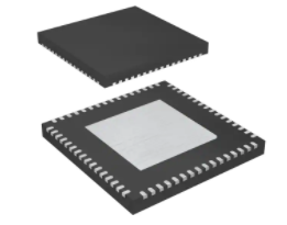


 工商网监
湘ICP备2023018690号
工商网监
湘ICP备2023018690号
