Le87271
Datasheet
xDSL CPE Line Driver
Preliminary
August, 2019
�xDSL CPE Line Driver
Contents
1 Revision History ............................................................................................................................. 1
1.1 Revision 3.0 ........................................................................................................................................ 1
1.2 Revision 2.0 ........................................................................................................................................ 1
1.3 Revision 1.0 ........................................................................................................................................ 1
2 Product Overview .......................................................................................................................... 2
2.1 Features .............................................................................................................................................. 2
2.2 Applications ........................................................................................................................................ 2
2.3 Block Diagram ..................................................................................................................................... 3
3 Pin Descriptions ............................................................................................................................. 4
3.1 Pin Description ................................................................................................................................... 5
4 Electrical Specifications .................................................................................................................. 6
4.1 Absolute Maximum Ratings ................................................................................................................ 6
4.1.1
Thermal Resistance ................................................................................................................................. 6
4.1.2
Package Assembly ................................................................................................................................... 6
4.1.3
Operating Ranges .................................................................................................................................... 7
4.2 Device Specifications .......................................................................................................................... 7
4.3 Operational States ............................................................................................................................ 10
4.3.1
TX States ................................................................................................................................................ 10
4.3.2
Power Down State ................................................................................................................................. 10
4.3.3
Thermal Shut-down ............................................................................................................................... 10
5 Applications ................................................................................................................................. 11
5.1 Typical Application Circuits ............................................................................................................... 11
5.1.1
IREF ........................................................................................................................................................ 12
5.1.2
Input Consideration ............................................................................................................................... 12
5.1.3
Output Driving Considerations .............................................................................................................. 12
5.1.4
Protection .............................................................................................................................................. 12
5.1.5
Power Supplies and Component Placement ......................................................................................... 12
6 Package Specifications ................................................................................................................. 13
6.1 Physical Dimension - 20-Pin Diagram ............................................................................................... 13
7 Ordering Information ................................................................................................................... 14
Microsemi Proprietary and Confidential. PS-0331435 Le87271 Datasheet Revision 3.0
�xDSL CPE Line Driver
1
Revision History
The revision history describes the changes that were implemented in the document. The changes are
listed by revision, starting with the most current publication.
1.1
Revision 3.0
Revision 3.0 of this document was published in August 2019. The following is a summary of the changes.
Features and applications of the Le87271 device were updated. For more information, see the
Product Overview (see page 2) section.
Section Output Driving Considerations (see page 12) was edited.
1.2
Revision 2.0
Moved from Advance to Preliminary.
1.3
Revision 1.0
Revision 1.0 was published in December 2018. Revision 1.0 was the first publication of this document.
Microsemi Proprietary and Confidential. PS-0331435 Le87271 Datasheet Revision 3.0
1
�xDSL CPE Line Driver
2
Product Overview
The Le87271 device is a single-channel differential amplifier designed to work in Customer Premise
Equipment (CPE) systems. It provides multiple bias levels to optimize power and performance. In
addition, the line driver features a power-down state, which forces low power. The control pins respond
to input levels that can be generated with a standard GPIO.
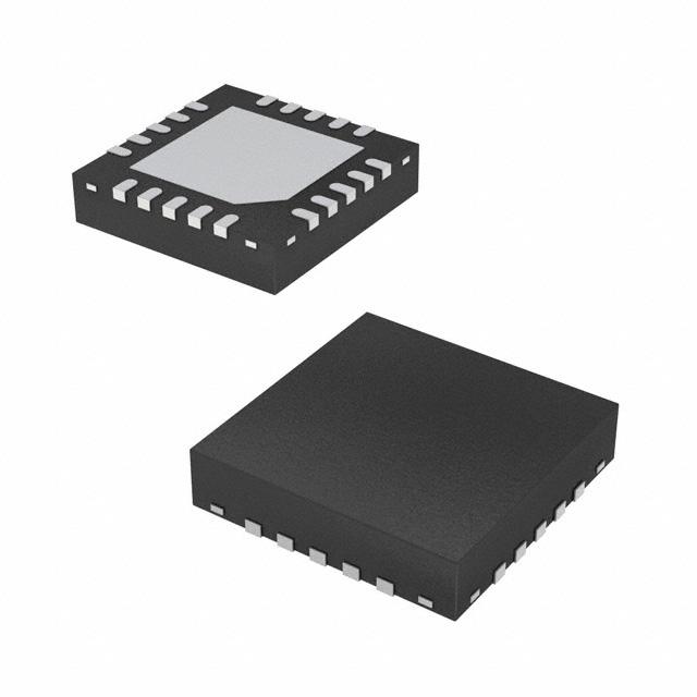
The Le87271 device is available in a 20-pin (4 mm x 4 mm) QFN package with an exposed pad for
enhanced thermal conductivity.
2.1
Features
The Le87271 device has the following important features:
High-power differential output
Delivers line power up to 14 dBm
Operates at 14 V ±10 %
Class AB amplifiers
Four biased up states for VDSL applications
Four biased up states for ADSL applications
Power down states
Thermal shutdown circuitry
Miniature 4 mm x 4 mm thermally enhanced package
RoHS compliant
2.2
Applications
The following applications use the Le87271 device.
CPE Line Driver for ADSL, ADSL2, and ADSL2+
CPE Line Driver for VDSL2, all profiles up to 17a, 30a, and 35b.
Microsemi Proprietary and Confidential. PS-0331435 Le87271 Datasheet Revision 3.0
2
�xDSL CPE Line Driver
2.3
Block Diagram
The following figure shows the Le87271 block diagram.
Figure 1 • Line Driver Block Diagram
Microsemi Proprietary and Confidential. PS-0331435 Le87271 Datasheet Revision 3.0
3
�xDSL CPE Line Driver
3
Pin Descriptions
The Le87271 device has 20 pins that are described in the following section.
The following figure shows the top-view of the Le87271 pin configuration.
Figure 2 • Pin Diagram
Note: The device incorporates an exposed die pad on the underside of its package. The pad acts as a
heat sink and must be connected to a copper plane through the thermal plane for proper heat
dissipation. It is internally connected to VSS, but on the board, it should be connected to ground.
Microsemi Proprietary and Confidential. PS-0331435 Le87271 Datasheet Revision 3.0
4
�xDSL CPE Line Driver
3.1
Pin Description
The following table lists the functional pin descriptions of the Le87271 device.
Table 1 • Pin Descriptions
Pin
Pin Name
Pin Type
1
NC
No connects, no internal connection
2
NC
No connects, no internal connection
3
C0
Input
Logic level inputs for state control
4
C1
Input
Logic level inputs for state control
5
C2
Input
Logic level inputs for state control
6
NC
No connects, no internal connection
7
IREF
Bias current reference
8
VDD
Power supply
9
VDD_N
Power supply
10
NC
No connects, no internal connection
11
OUT_N
12
NC
13
VSS
14
NC
15
OUT_P
16
NC
No connects, no internal connection
17
VDD_P
Power supply
18
VDD
Power supply
19
IN_P
Input
Line driver differential input
20
IN_N
Input
Line driver differential input
Output
Description
Line driver differential output
No connects, no internal connection
Ground
Ground
No connects, no internal connection
Output
Line driver differential output
Microsemi Proprietary and Confidential. PS-0331435 Le87271 Datasheet Revision 3.0
5
�xDSL CPE Line Driver
4
Electrical Specifications
The following section shows the electrical specifications of the Le87271 device.
4.1
Absolute Maximum Ratings
The following section shows the absolute maximum ratings, thermal resistance, and operating ranges of
the Le87271 device.
The following table lists the absolute maximum ratings of the Le87271 device.
Table 2 • Absolute Maximum Ratings
Names
Range
Unit
VDD with respect to VSS
–0.3 to 16
V
Control inputs with respect to VSS
–0.3 to 4
Junction temperature
–40 to 150
ESD immunity (Human Body Model)
JESD22 Class 2 complaint
ESD immunity (Charge Body Model)
JESD22 class IV compliant
°C
Continuous operation above 145 °C junction temperature may degrade the device reliability. The typical
TSD temperature is 170 °C, with 20 °C hysteresis.
4.1.1
Thermal Resistance
Thermal performance of a thermally enhanced package is assured through an optimized PCB layout. The
specified performance requires that the exposed thermal pad should be soldered to an equally sized
exposed copper surface, which, in turn, conducts heat through multiple vias to larger internal copper
planes.
The following table lists the simulation results of a device mounted on a 4-layer JEDEC PCB with 12
thermal vias in still air. These numbers are only for reference.
Table 3 • Thermal Resistance Specifications
4.1.2
Names
Value
Unit
Maximum device power dissipation, continuous - TA = 150 °C
1.37
W
Junction to ambient thermal resistance, θJA
47.5
°C/W
Junction-to-board thermal resistance, θJB
25.8
Junction-to-case bottom (exposed pad) thermal resistance, θJP
11.7
Junction-to-top characterization parameter, θJC
30.8
Package Assembly
Green package devices are assembled with enhanced, environmental-friendly lead-free, halogen-free,
and antimony-free materials. The leads possess a matte-tin plating, which is compatible with
conventional board assembly processes or newer lead-free board assembly processes.
Microsemi Proprietary and Confidential. PS-0331435 Le87271 Datasheet Revision 3.0
6
�xDSL CPE Line Driver
See IPC/JEDEC J-Std-020 for recommended peak soldering temperature and solder re-flow temperature
profile.
4.1.3
Operating Ranges
Microsemi guarantees the performance of this device over the –40 °C to 85 °C temperature range by
conducting electrical characterization and a single insertion production test coupled with periodic
sampling. These procedures comply with the Telcordia GR-357-CORE generic requirements for assuring
the reliability of components used in telecommunications equipment.
The following table lists the operating ranges used in this device.
Table 4 • Operating Ranges
4.2
Name
Unit
Minimum
Typical
Maximum
Supply voltage, VDD/VDD_P/VDD_N
V
12.6
14
15.4
Ambient temperature
°C
–40
25
85
Line impedance
Ω
80
100
150
Device Specifications
The following section shows the DC characteristics, AC characteristics, and recommended operating
conditions of the Le87271 device.
Typical values are characteristics of the Le87271 device and are the result of the engineering evaluation.
Minimum and maximum values apply across the operating temperature range and the entire supply
range does not vary unless otherwise specified.
Note: Typical values are for information purposes only and are not part of the testing requirement.
Typical Conditions: VDD = VDD_P = VDD_N = 14 V; RL = 50 Ω differential load; RREF = 75 KΩ; TA = 25 °C.
For more information, see the Basic Test Circuit (see page 9) figure.
The following table lists the electrical specifications. As VDD, VDD_P, and VDD_N are expected to be tied
together, IVDD represents the total current through these three pins, and PVDD represents the total
supply power.
Table 5 • Electrical Specifications
Symbol
Parameter Description
Condition
Min
Typ
Max
Unit
IVDD
Quiescent supply
ATX4
14.8
17.4
20.0
mA
ATX3
13.3
15.6
17.9
mA
ATX2
10.7
12.6
14.5
mA
ATX1
9.4
11.0
12.7
mA
Note
current
IVDD
Quiescent supply
current
IVDD
Quiescent supply
current
IVDD
Quiescent supply
current
Microsemi Proprietary and Confidential. PS-0331435 Le87271 Datasheet Revision 3.0
7
�xDSL CPE Line Driver
Symbol
Parameter Description
Condition
Min
Typ
Max
Unit
IVDD
Quiescent supply
VTX4
19.3
22.7
26.1
mA
VTX3
17.8
20.9
24.0
mA
VTX2
15.1
17.8
20.5
mA
VTX1
13.7
16.1
18.5
mA
600
mW
Note
current
IVDD
Quiescent supply
current
IVDD
Quiescent supply
current
IVDD
Quiescent supply
current
PVDD
Supply power
PLine = 13 dBm
VOUT
Output voltage
Between OUT_P/N
10.5
Vpkd
IOUT
Drive current
Through OUT_P/N
240
mApk
2
iN
Input-referred noise
VTX States
6
nV/rtHz
1
iN
Input-referred noise
ATX States
4
nV/rtHz
1
AV
Gain
8.20
V/V
BW
Bandwidth
–3 dB, ATX4 States
146
MHz
1
BW
Bandwidth
–3 dB, ATX3 States
140
MHz
1
BW
Bandwidth
–3 dB, ATX2 States
90
MHz
1
BW
Bandwidth
–3 dB, ATX1 States
72
MHz
1
BW
Bandwidth
–3 dB, VTX4 States
200
MHz
1
BW
Bandwidth
–3 dB, VTX3 States
190
MHz
1
BW
Bandwidth
–3 dB, VTX2 States
148
MHz
1
BW
Bandwidth
–3 dB, VTX1 States
137
MHz
1
AVF
Gain flatness
f < Signal BW
–0.3
dB
1, 3
MTPR
Missing tone power
VDSL, PAR = 6.8
64
dBc
1
dBc
1
7.88
8.03
0.3
1
ratio
MTPR
Power ratio
ADSL, PAR = 6.3
90
RI
Input impedance
Differential
12
RO
Output impedance
Differential
0
CMRR
Common mode
f < Signal BW
15
18
kΩ
1
Ω
1
dB
1, 3
dB
1, 3
35
rejection ratio
PSRR
Power supply rejection
f < Signal BW
50
Power down state
0.4
ratio
IVDD
Quiescent supply
0.6
0.8
mA
current
ON
Output noise
Power down state
0.9
nV/rtHz
1
680
Ω
1
(100 kHz–30 MHz)
RO
Output impedance
Power down state
(Differential)
VIH
Input high voltage
2.0
VIL
Input low voltage
VIM
Input middle voltage
C0
1.4
IIH
Input high current
VIH = 3 V, C0
15
V
0.8
V
1.5
1.6
V
50
85
µA
Microsemi Proprietary and Confidential. PS-0331435 Le87271 Datasheet Revision 3.0
8
�xDSL CPE Line Driver
Symbol
Parameter Description
Condition
Min
Typ
Max
Unit
IIH
Input high current
VIH = 3 V, C1, C2
60
120
180
µA
IIL
Input low current
VIL = 0 V, C0
–85
–50
–15
µA
IIL
Input low current
VIL = 0 V, C1, C2
–2
0
2
µA
Zin
Logic input impedance
25
Note
kΩ
Notes:
1. Not tested in production. Guaranteed by design and characterization.
2. For line impedance of 80 Ω.
3. Frequency range within signal bandwidth is 552 kHz for ADSL and 30 MHz for VDSL.
The following figure shows the basic test circuit of the Le87271 device.
Figure 3 • Basic Test Circuit
Microsemi Proprietary and Confidential. PS-0331435 Le87271 Datasheet Revision 3.0
9
�xDSL CPE Line Driver
4.3
Operational States
Operating state is controlled through three input pins: C0, C1, and C2. C1 and C2 are binary inputs with
internal pull-down resistors. C0 is a tri-state input with an internal resistor pulling to the middle (M)
logic value if the pin is not driven. If the inputs are not driven, the line driver by default changes into the
power down state.
The following table lists the operational state control of the Le87271 device.
Table 6 • Operational State Control
C2
C1
C0
State
Device State
H
H
M
ATX4
Low noise for ADSL
H
L
H
ATX3
Low noise for ADSL
H
H
L
ATX2
Low noise for ADSL
H
H
H
ATX1
Low noise for ADSL
L
H
M
VTX4
High speed for VDSL
L
L
H
VTX3
High speed for VDSL
L
H
L
VTX2
High speed for VDSL
L
H
H
VTX1
High speed for VDSL
X
L
L
Power down
Amplifiers off, high impedance outputs
X
L
M
Power down
Amplifiers off, high impedance outputs
X
X
X
Thermal
Amplifiers off, high impedance outputs
shut-down
4.3.1
TX States
In TX states, the amplifiers are fully active with gain from INx to OUTx. TX states provide four steps of
bias current to the amplifiers. This allows some selection of power versus linearity in the line driver
performance. The TX states are further identified as ADSL states (lower bias current, lower noise) or
VDSL states (higher bias current, higher bandwidth).
4.3.2
Power Down State
Line driver amplifiers are turned off, and there is no gain from INx to OUTx. The amplifier outputs are
high-impedance. The gain-setting resistors around the amplifiers remain in place and present a
differential impedance at the OUT_P/N.
4.3.3
Thermal Shut-down
Thermal shut-down (TSD) is activated at high silicon temperature. Amplifiers are turned off. There is
hysteresis in the TSD temperature threshold. After the silicon cools down below the threshold level, the
line driver returns to the operating state indicated by the control inputs.
Microsemi Proprietary and Confidential. PS-0331435 Le87271 Datasheet Revision 3.0
10
�xDSL CPE Line Driver
5
Applications
This section shows the applications that use the Le87271 device, and the block diagram describe the
functionalities.
5.1
Typical Application Circuits
The following figure shows the typical application circuit of the Le87271 device.
Figure 4 • Typical Application Circuit
The following table lists the resistors and capacitors with the tolerance values.
Table 7 • Application Circuit Names and Values
Names
Type
Value
Unit
Tolerance
Rating
RREF
Resistor
75.0
kΩ
1%
0402
RSP
Resistor
12.4
Ω
1%
0805
RSN
Resistor
12.4
Ω
1%
0805
CS1
Capacitor
1
µF
20%
X7R, 25 V
CS2
Capacitor
0.01
µF
20%
X7R, 25 V
D1
Diode Bridge
BAV99
D2
Diode Bridge
BAV99
CTXP
Capacitor
0.047
µF
20%
X7R, 25 V
CTXN
Capacitor
0.047
µF
20%
X7R, 25 V
Microsemi Proprietary and Confidential. PS-0331435 Le87271 Datasheet Revision 3.0
11
�xDSL CPE Line Driver
5.1.1
IREF
Connect RREF from IREF pin to ground. DC current through RREF provides reference bias current for the
device.
5.1.2
Input Consideration
The inductance of the trace from driving source to CTXP or CTXN should be less than 100 nH to avoid
any ringing or oscillation.
5.1.3
Output Driving Considerations
Inside the amplifier, there is no current limit mechanism. RSA and RSB in a few ohms enable to limit
current viewed by the line driver in case of large fault transients. If a DC current path exists between the
two outputs, DC current can flow through the outputs. With RSP and RSN resistors as shown in place,
however, any DC current will be trivial, and therefore, such DC blocking capacitor may not be needed.
5.1.4
Protection
The line driver has thermal shutdown protection. Amplifiers turn off and outputs appear as
high-impedance if the silicon temperature rises above the TSD temperature.
As shown in the Typical Application Circuit (see page 11) figure, diode bridges may be used at the
secondary side of the data transformer to clamp transients between the VDD and VSS rails. It is possible
that additional transient clamping devices are needed to protect on the line side of the data transformer
the isolation of the data transformer in the event of common mode faults.
5.1.5
Power Supplies and Component Placement
The power supply should be well bypassed with decoupling placed close to the Le87271 device.
Microsemi Proprietary and Confidential. PS-0331435 Le87271 Datasheet Revision 3.0
12
�xDSL CPE Line Driver
6
Package Specifications
This section shows the package information of the Le87271 device.
6.1
Physical Dimension - 20-Pin Diagram
The following figure shows the package drawing for the Le87271 device. The drawing contains the top,
bottom, and side views.
Figure 5 • Physical Dimension - 20 Pins
Note: Packages might have mold tooling markings on the surface. These markings have no impact on the
form, fit, or function of the device. Markings vary with the mold tool used during manufacturing.
Microsemi Proprietary and Confidential. PS-0331435 Le87271 Datasheet Revision 3.0
13
�xDSL CPE Line Driver
7
Ordering Information
The following table lists the ordering information of Le87271.
Part Order Number
Description
Packing System
Le87271EQC
20-pin, 4mm x 4mm QFN green package with an exposed pad
Tray
Le87271EQCT
20-pin, 4mm x 4mm QFN green package with an exposed pad
Tape and reel
Note: The green package is halogen free and meets the RoHS2 directive 2011/65/EU of the European
Council to minimize the environmental impact of electrical equipment.
Microsemi Proprietary and Confidential. PS-0331435 Le87271 Datasheet Revision 3.0
14
�xDSL CPE Line Driver
Microsemi makes no warranty, representation, or guarantee regarding the information contained herein or the suitability of its products and services
for any particular purpose, nor does Microsemi assume any liability whatsoever arising out of the application or use of any product or circuit. The
products sold hereunder and any other products sold by Microsemi have been subject to limited testing and should not be used in conjunction with
mission-critical equipment or applications. Any performance specifications are believed to be reliable but are not verified, and Buyer must conduct and
complete all performance and other testing of the products, alone and together with, or installed in, any end-products. Buyer shall not rely on any data
and performance specifications or parameters provided by Microsemi. It is the Buyer's responsibility to independently determine suitability of any
products and to test and verify the same. The information provided by Microsemi hereunder is provided "as is, where is" and with all faults, and the
entire risk associated with such information is entirely with the Buyer. Microsemi does not grant, explicitly or implicitly, to any party any patent rights,
licenses, or any other IP rights, whether with regard to such information itself or anything described by such information. Information provided in this
document is proprietary to Microsemi, and Microsemi reserves the right to make any changes to the information in this document or to any products
and services at any time without notice.
Microsemi Headquarters
One Enterprise, Aliso Viejo,
CA 92656 USA
Within the USA: +1 (800) 713-4113
Outside the USA: +1 (949) 380-6100
Sales: +1 (949) 380-6136
Fax: +1 (949) 215-4996
Email: sales.support@microsemi.com
www.microsemi.com
© 2019 Microsemi. All rights reserved. Microsemi and the Microsemi logo
are trademarks of Microsemi Corporation. All other trademarks and service
marks are the property of their respective owners.
Microsemi, a wholly owned subsidiary of Microchip Technology Inc. (Nasdaq: MCHP), offers a comprehensive portfolio of semiconductor and system
solutions for aerospace & defense, communications, data center and industrial markets. Products include high-performance and radiation-hardened
analog mixed-signal integrated circuits, FPGAs, SoCs and ASICs; power management products; timing and synchronization devices and precise time
solutions, setting the world's standard for time; voice processing devices; RF solutions; discrete components; enterprise storage and communication
solutions; security technologies and scalable anti-tamper products; Ethernet solutions; Power-over-Ethernet ICs and midspans; as well as custom design
capabilities and services. Microsemi is headquartered in Aliso Viejo, California, and has approximately 4,800 employees globally. Learn more at www.
microsemi.com.
PS-0331435
Microsemi Proprietary and Confidential. PS-0331435 Le87271 Datasheet Revision 3.0
15
�