LX7176A
4A Step-Down-Regulator
Production Datasheet
Description
Features
The LX7176A is a 4A step-down regulator with
integrated MOSFETs packaged in a space saving QFN12
2mm x 2mm for today’s mobile devices. It uses an ultra
fast, constant frequency hysteretic control method to
minimize external filter components while maintaining
excellent regulation. The LX7176A reference voltage is
0.6V.
0-4A Step-down Regulator
The LX7176A operates from 3V to 5.5V rails and outputs
0.6V to 100% of the input voltage.
Automatically switches to DCM switching
under light loads to improve efficiency
Cycle-by-cycle current limiting protects against overcurrent conditions. Hiccup mode provides protection for
heavy over-load or short-circuit faults.
Thermal
protection shuts down the regulator under overtemperature conditions. Over voltage conditions will
immediately shut off the output to protect against
permanent damage. The LX7176A automatically restarts
when all fault conditions are cleared. Internal soft start
circuitry limits start up inrush currents.
VIN
1
10
10µF
X5R
PVIN
SW
2, 11
0.47µH
FB
EN
6
NC
5
PGOOD
PGND
3, 12
AGND
4
PGOOD
Figure 1: Typical Application Diagram
Copyright © 2013
Rev. 1.2 09/21/15
Enable and Power Good Function
Internal soft-start
Cycle-by-Cycle Over Current Protection
Hiccup Mode protects against short circuit
faults
GND
R2
OUT
9
Input under voltage and over voltage
protection
7
LX7176A
500k
100% Duty Ratio Operation
Applications
22µF, X5R
R1
8
CCM switching at a constant 1.65MHz
VOUT
VIN
10µF
X5R
Hysteretic control offers best transient
response
RoHS Compliant
SW
GND
Operational Input Supply Voltage Range:
3V-5.5V (short durations to 6.5V.)
High Performance HDD
LCD TV
Notebook/Netbook
Server and Workstations
Video Cards
PoE Powered Devices Smart Phone
Microsemi
Analog Mixed Signal Group
One Enterprise Aliso Viejo, CA 92656 USA 1-800-713-4113, 1-949-380-6100, fax 1-949-215-4996
Page 1
�LX7176A
4A Step-Down-Regulator
Production Datasheet
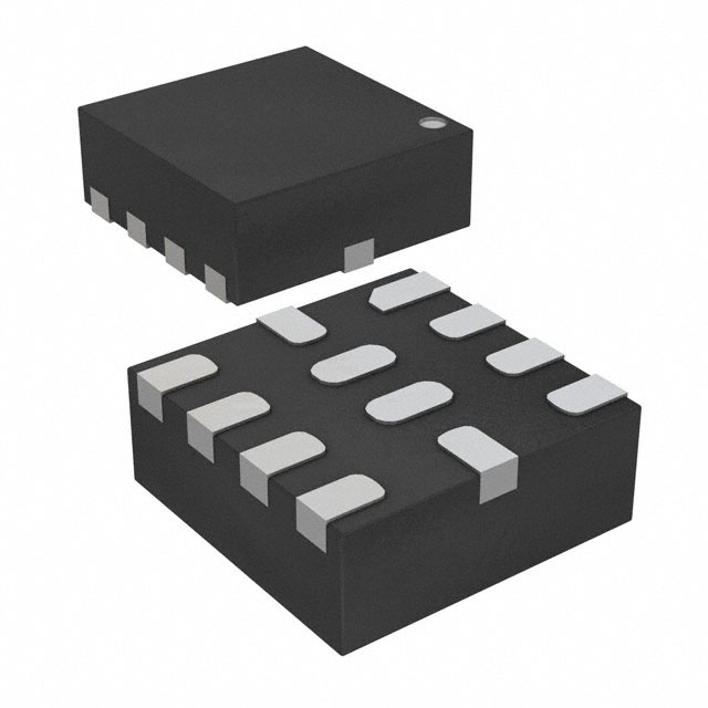
Pin Configuration and Pinout
• 76A
YWWL
• Pin 1 Indicator, YWWL = Year/Week/Lot Code
RoHS / Pb-free Matte Tin Pin Finish
Figure 2: Pinout
Ordering Information
Ambient
Temperature
Type
Package
Part Number
0°C to 85°C
RoHS compliant, Pb-free
QFN 2x2mm 12L
LX7176ACLQ
LX7176ACLQ-TR
Packaging
Type
Bulk
Tape and Reel
Thermal Properties
Thermal Resistance(θJA)
QFN 2x2mm 12L
Typ
30
Units
°C/W
Note: The JA number assumes no forced airflow. Junction Temperature is calculated using TJ = TA + (PD x JA). In particular,
θJA is a function of the PCB construction. The stated number above is for a four-layer board in accordance with JESD-51
(JEDEC).
Copyright © 2013
Rev. 1.2 09/21/15
Microsemi
Analog Mixed Signal Group
One Enterprise Aliso Viejo, CA 92656 USA 1-800-713-4113, 1-949-380-6100, fax 1-949-215-4996
Page 2
�LX7176A
4A Step-Down-Regulator
Production Datasheet
Pin Description
Pin Number
Pin Designator
1, 10
PVIN
2, 11
3, 12
4
SW
PGND
AGND
5
NC
6
OUT
7
FB
8
EN
9
PG
Copyright © 2013
Rev. 1.2 09/21/15
Description
Supply Voltage. Bypass PVIN to ground plane as close as possible to
the IC.
Switch Output. Drives the external L-C filter.
Power Ground. Connect to ground plane.
Analog Ground. Connect to ground plane.
No connect pin. Leave floating. Serves as SCL when accessing the
serial port.
Output Voltage Sense Pin – This pin monitors the output voltage.
Serves as SDA when accessing the serial port. Digital signals at this
pin will be capacitively coupled onto FB and disturb the output
voltage.
Feedback – Analog input, monitors the output voltage either directly
or through a resistor divider.
Enable – Digital input. Force high to enable the IC.
Power Good – Open drain digital output. Pulls low to indicate a fault
condition. Requires an external pull up resistor. Also used to
monitor selected internal signals.
Microsemi
Analog Mixed Signal Group
One Enterprise Aliso Viejo, CA 92656 USA 1-800-713-4113, 1-949-380-6100, fax 1-949-215-4996
Page 3
�LX7176A
4A Step-Down-Regulator
Production Datasheet
Block Diagram
Figure 3: Block Diagram
Copyright © 2013
Rev. 1.2 09/21/15
Microsemi
Analog Mixed Signal Group
One Enterprise Aliso Viejo, CA 92656 USA 1-800-713-4113, 1-949-380-6100, fax 1-949-215-4996
Page 4
�LX7176A
4A Step-Down-Regulator
Production Datasheet
Absolute Maximum Ratings
Performance is not necessarily guaranteed over this entire range. These are maximum stress ratings
only. Exceeding these ratings, even momentarily, can cause immediate damage, or negatively impact
long-term operating reliability.
Parameter
PVIN, EN, PG, OUT, FB, SW to PGND
AGND to PGND
SW to PGND (Shorter than 50ns)
Junction Temperature Range
Storage Temperature Range
Peak Lead Soldering Temperature (40s, reflow)
Min
-0.3
-0.3
-2
0
-65
Max
7
0.3
7
150
150
260 (+0, -5)
Units
V
V
V
°C
°C
°C
Operating Ratings
Performance is generally guaranteed over this range as further detailed below under Electrical
Characteristics.
Parameter
Input Voltage
Output Voltage
Output Current (VIN = 3V to 5V)
Ambient Temperature
Min
3.0
0.6
0
0
Max
5.5
5.5
4
85
Units
V
V
A
°C
Note: Corresponding Max Junction Temperature is 125°C
Copyright © 2013
Rev. 1.2 09/21/15
Microsemi
Analog Mixed Signal Group
One Enterprise Aliso Viejo, CA 92656 USA 1-800-713-4113, 1-949-380-6100, fax 1-949-215-4996
Page 5
�LX7176A
4A Step-Down-Regulator
Production Datasheet
Electrical Characteristics
Unless otherwise specified, the following specifications apply over the operating ambient temperature
of 0°C ≤ TA ≤ 85°C with the following test conditions: PVIN = 5V. Typical parameters refers to T J = 25°C.
VOUT = 0.9V. VOUT is disconnected from FB for open loop tests. Iload = 0,. EN=high, GBD specifications are
guaranteed by design and/or characterization and are not tested on a production basis.
Symbol
PVIN
IQPSM
ISLEEP
UVLORISING
UVLOHYST
OVPR
OVPF
VREF
VREF
TSS
THICCUP
VOUT
VOUT
Parameter
PSM Bias Current
Input Current at
Shutdown
Under Voltage
Rising Threshold
UVLO Hysteresis
Over Voltage
Rising Threshold
Over Voltage
Falling Threshold
VOUT Accuracy
FBIL
FBUV
RDISC
Load Regulation
FB Input Current
FB Under Voltage
Threshold
Output Discharge
Resistance
Min
Typ
Enable PSM
280
EN = low, TJ = 25°C
0.1
PVIN rising
PVIN falling
PVIN rising. Will also trigger on
DV/DT > 1V/µs
PVIN falling
Reference Voltage
VREF Slew Rate
Hiccup Time
Line Regulation
VOUTLR
Conditions
VOUT is set to 0.9V with 0.1%
feedback resistors. PVIN = 5V, ,
0°C to 85°C.
ILOAD = 0.1A
VIN from 3V to 5V, (in DCM)
VOUT = 0.9V. Note
ILOAD = 2.5A
1
(in CCM)
VOUT = 0.9V, IOUT = 0A to 4A .
Note 1
Max
µA
3
µA
2.8
V
0.2
V
6.1
V
5.5
5.85
V
0.594
0.6
3.75
1.2
0.606
V
mV/µs
ms
0.891
0.9
0.909
V
0.01
%/V
0.06
-0.06
%/A
1
VOUT below this threshold will
initiate a hiccup sequence.
EN = low
Units
80
80
314
µA
%VREF
500
Ω
SW
RDSON_H
Copyright © 2013
Rev. 1.2 09/21/15
High Side On
Resistance
46
Microsemi
Analog Mixed Signal Group
One Enterprise Aliso Viejo, CA 92656 USA 1-800-713-4113, 1-949-380-6100, fax 1-949-215-4996
mΩ
Page 6
�LX7176A
4A Step-Down-Regulator
Production Datasheet
Symbol
RDSON_L
IRATED
ICL
TSH
TH
Parameter
Low Side On
Resistance
Rated Output
Current
Current Limit
Thermal
Shutdown
Threshold¹
Thermal
Shutdown
Hysteresis¹
FSW
PWM Switching
Frequency
EN
VIH
VIL
IIN
PG
Input High
Input Low
Input Current
VPG90
VPG110
VPGHY
PGRDSON
PGILEAK
PGOOD VOUT
Lower Threshold
PGOOD VOUT
Upper Threshold
Hysteresis
PGOOD Pull-down
Resistance
PGOOD Leakage
Current
Conditions
Min
Typ
Max
21
PVIN = 3V to 5V. Note 1
Peak inductor current. PVIN = 3V
to 5V . Note 1
mΩ
4
6.3
Units
A
7.4
9
A
Note 1
150
°C
Note 1
20
°C
VOUT / VIN ≥ 35%, T=25°C, Note 1
1.55
1.65
1.75
MHz
1.2
V
V
µA
0.4
0.01
1
VOUT rising, percentage of VREF
90
%
VOUT falling, percentage of VREF
110
%
5
%
Percentage of VREF
TJ = 25°C
13
50
Ω
0
1
µA
Note 1: These parameters are not tested, but guaranteed by design and characterization.
Copyright © 2013
Rev. 1.2 09/21/15
Microsemi
Analog Mixed Signal Group
One Enterprise Aliso Viejo, CA 92656 USA 1-800-713-4113, 1-949-380-6100, fax 1-949-215-4996
Page 7
�LX7176A
4A Step-Down-Regulator
Production Datasheet
Typical Performance Curves (Efficiency)
100%
90%
Efficiency
80%
70%
60%
50%
VOUT = 0.9V
VOUT = 1.8V
VOUT = 3.3V
40%
30%
1
10
100
Load Current (mA)
1000
Figure 4: LX7176A Efficiency with VIN = 5V, L = 0.47µH, COUT = 22µF
Copyright © 2013
Rev. 1.2 09/21/15
Microsemi
Analog Mixed Signal Group
One Enterprise Aliso Viejo, CA 92656 USA 1-800-713-4113, 1-949-380-6100, fax 1-949-215-4996
Page 8
�LX7176A
4A Step-Down-Regulator
Production Datasheet
Step Response(Load Current = 1.5A to 4A, L = 0.47μH, COUT = 22μF)
Typical Performance Curves
Figure 5. Step Load
Figure 6. Step Load Rising Edge
Figure 7. Step Load Falling Edge
Copyright © 2013
Rev. 1.2 09/21/15
Microsemi
Analog Mixed Signal Group
One Enterprise Aliso Viejo, CA 92656 USA 1-800-713-4113, 1-949-380-6100, fax 1-949-215-4996
Page 9
�LX7176A
4A Step-Down-Regulator
Production Datasheet
Theory of Operation
Basic Operation
The LX7176A compares the FB voltage to an
internal reference, VREF. When FB is lower than
Vref, the upper switch turns on and the lower
LX7166
switch turns off. When FB is higher than VREF, the
upper switch turns off and the lower switch turns
on. An internal ramp and a frequency control loop
keep the switching frequency constant when in
constant conduction mode (CCM) over a wide
range of output capacitor values and parasitic
components (i.e. ESR, ESL).
At light loads, the converter automatically reduces
the switching frequency to optimize conversion
efficiency.
a hiccup sequence will be initiated where both
output switches are shut off for 1.2ms before
initiating another soft start. This protects against a
crowbar short circuit. FB under voltage detection is
not active during startup.
Setting the Output Voltage
The reference voltage is 0.6V
R
VOUT 1 1 VREF
R2
(1)
Where R1 is high side feedback divider resistor, R2 is
low side feedback divider resistor, VREF is 0.6V.
Startup
The LX7176A is enabled when EN is high and PVIN
rises above the UVLO threshold. At start up, after
all the internal bias voltages and currents stabilize,
VREF ramps up from 0V to the target voltage at the
defined slew rate. While VREF ramps, PGOOD is
held low. At the end of the ramp time, PGOOD is
allowed to go high if the FB has reached the
PGOOD rising threshold.
Over Current Protection
The LX7176A protects against all types of short
circuit conditions. Cycle by cycle over current
protection turns off the upper switch when the
current exceeds the ICL threshold. When this
occurs, the upper switch is kept off for about
360ns before being allowed to turn on again. After
startup, if FB drops below the FBUV threshold,
Copyright © 2013
Rev. 1.2 09/21/15
Microsemi
Analog Mixed Signal Group
One Enterprise Aliso Viejo, CA 92656 USA 1-800-713-4113, 1-949-380-6100, fax 1-949-215-4996
Page 10
�LX7176A
4A Step-Down-Regulator
Production Datasheet
Recommended Output Filter Components
The following tables show recommended feedback
component values (RHIGH, RLOW, Cff) for different
input/output voltages, power inductor (L), and
output capacitance (C) values that result in
optimum closed loop response of the regulator in
each case. The estimated crossover frequency is
also shown in the table in each case. If the L*C
factor exceeds a certain number the regulator
would run with low phase margin, or become
unstable. The L and C range provided in the table
provides 30°, or higher of phase margin. Therefore,
it is not recommended to increase L*C factor
beyond what is given in the table.
It is a good practice to determine L such that the
peak-to-peak inductor ripple current in continuous
conduction mode operation is roughly equal to 30%
of converter’s rated output current. In general,
increasing the inductance slows down the closed
loop response of the regulator. Hence, for
applications that require fast line/load transient
response, lower inductance values should be
preferred over larger ones. Output capacitance can
be determined based on desired output ripple
voltage staying within the limits provided in the
table depending on the inductance value.
VIN
(V)
VOUT
(V)
L
(µH)
COUT
(µF)
RHIGH
(kΩ)
RLOW
(kΩ)
4x22
2.2
47
3x22
33
100
1x22
12
150
73
27
4x22
3x22
12
0.9
200
5x22
92
22
3x22
60
120
2x22
1
GND
10
PVIN
SW
2, 11
L
1x22
300
5x22
140
10
3x22
10µF
X5R
FB
8
EN
170
220
2x22
0
1x22
280
575
5x22
0.33
170
180
6.8
3x22
220
280
Cout
VIN
Cff
10µF
X5R
VOUT
110
130
12
4x22
0.47
120
1x22
4x22
5.0
84
100
2x22
1.0
70
2x22
5x22
1.5
F
crossover
(kHz)
83
4x22
VIN
Cff
(pF)
Rhigh
GND
7
LX7176A
2x22
1x22
Rlow
7.5
15
0
400
625
6
OUT
500k
NC
9
5
PGOOD
PGND
3, 12
AGND
4
PGOOD
Copyright © 2013
Rev. 1.2 09/21/15
Microsemi
Analog Mixed Signal Group
One Enterprise Aliso Viejo, CA 92656 USA 1-800-713-4113, 1-949-380-6100, fax 1-949-215-4996
Page 11
�LX7176A
4A Step-Down-Regulator
Production Datasheet
Recommended Output Filter Components - Continued
VIN
(V)
VOUT
(V)
L
(µH)
2.2
1.5
COUT
(µF)
RHIGH
(kΩ)
RLOW
(kΩ)
3.0
33
76
1x22
12
110
3x22
27
74
2x22
12
140
5x22
68
22
93
2x22
120
60
0.47
Cff
(pF)
F
crossover
(kHz)
49
12
2x22
1.5
6.8
150
5x22
58
4x22
68
6.8
3x22
240
200
5x22
77
6.8
4x22
1.0
3x22
92
120
325
2x22
5x22
130
1x22
260
150
5x22
110
6.8
3x22
190
2x22
240
1x22
0
0
4x22
0.47
475
2x22
0.33
130
130
0
3x22
120
180
190
60
1x22
475
5x22
150
4x22
240
120
190
0
3x22
2x22
60
Microsemi
Analog Mixed Signal Group
One Enterprise Aliso Viejo, CA 92656 USA 1-800-713-4113, 1-949-380-6100, fax 1-949-215-4996
260
220
30
1x22
Copyright © 2013
Rev. 1.2 09/21/15
84
120
120
1x22
1.8
85
1x22
2x22
5.0
57
70
3x22
120
180
RLOW
(kΩ)
4x22
2.2
150
0
RHIGH
(kΩ)
1x22
4x22
0.33
10
COUT
(µF)
5x22
100
3x22
2x22
L
(µH)
190
120
5x22
4x22
VOUT
(V)
78
3x22
12
VIN
(V)
90
1x22
1x22
0.9
F
crossover
(kHz)
2x22
4x22
1.0
Cff
(pF)
500
Page 12
�LX7176A
4A Step-Down-Regulator
Production Datasheet
Recommended Output Filter Components - Continued
VIN
(V)
VOUT
(V)
L
(µH)
COUT
(µF)
RHIGH
(kΩ)
RLOW
(kΩ)
Cff
(pF)
5x22
1.8V
1.0
0.33
Copyright © 2013
Rev. 1.2 09/21/15
COUT
(µF)
RHIGH
(kΩ)
RLOW
(kΩ)
Cff
(pF)
F
crossover
(kHz)
42
4x22
67
2x22
81
60
3x22
110
1x22
100
1x22
5x22
42
4x22
49
12
3x22
6.8
6.8
79
1x22
140
5x22
55
6.8
240
120
1.5
60
2x22
3x22
2.2
50
3x22
64
22
5x22
75
4x22
87
3x22
100
2x22
140
1x22
540
120
240
5x22
100
4x22
5.0
3.3
1.0
170
120
33
3x22
140
79
2x22
190
87
1x22
325
1x22
150
5x22
170
5x22
76
4x22
4x22
89
2x22
0.47
L
(µH)
58
4x22
3.0
VOUT
(V)
5x22
2x22
1.5
VIN
(V)
36
4x22
2.2
F
crossover
(kHz)
0
0.47
33
200
3x22
240
110
2x22
350
2x22
160
1x22
1x22
350
5x22
5x22
97
4x22
120
3x22
3x22
0
0
150
2x22
240
1x22
525
4x22
0.33
225
50
0
220
540
120
22
3x22
260
325
2x22
1x22
450
475
135
Microsemi
Analog Mixed Signal Group
One Enterprise Aliso Viejo, CA 92656 USA 1-800-713-4113, 1-949-380-6100, fax 1-949-215-4996
30
0
525
Page 13
�LX7176A
4A Step-Down-Regulator
Production Datasheet
Package Dimensions
QFN 2x2mm 12L Package
MILLIMETERS
MIN
MAX
0.80
1.00
0.20 REF
0.20
0.30
INCHES
MIN
MAX
0.031
.039
0.008 REF
0.008
0.012
D
1.90
0.075
D2
E
e
0.50BSC
1.90
2.10
0.50 BSC
0.02BSC
0.075
0.083
0.020 REF
0.30
0.012
D2
D
L
10
b
9
1
8
2
7
3
6
4
E
e
5
Top View
b
A
A3
Bottom View
Dim
A
A3
B
L
2.10
0.45
0.083
0.018
Note:
1. Dimensions do not include mold flash or
protrusions; these shall not exceed 0.155mm
(.006”) on any side. Lead dimension shall not
include solder coverage.
2. Dimensions are in millimeters, inches for
reference only.
Side View
Recommended Footprint
Copyright © 2013
Rev. 1.2 09/21/15
Microsemi
Analog Mixed Signal Group
One Enterprise Aliso Viejo, CA 92656 USA 1-800-713-4113, 1-949-380-6100, fax 1-949-215-4996
Page 14
�LX7176A
4A Step-Down-Regulator
Production Datasheet
2.20mm
0.55mm
0.55mm
0.50mm
2.20mm
0.30mm
0.70mm
Disclaimer:
This PCB land pattern recommendation is based on information available to Microsemi by its suppliers. The actual land pattern to be used could be different depending on the materials and
processes used in the PCB assembly, end user must account for this in their final layout. Microsemi makes no warranty or representation of performance based on this recommended land pattern
PRODUCTION DATA – Information contained in this document is pre-production data and is
proprietary to Microsemi. It may not be modified in any way without the express written
consent of Microsemi. Product referred to herein is offered in pre-production form only and
may not have completed Microsemi’s Quality Assurance process for Release to Production.
Microsemi reserves the right to change or discontinue this proposed product at any time.
Copyright © 2013
Rev. 1.2 09/21/15
Microsemi
Analog Mixed Signal Group
One Enterprise Aliso Viejo, CA 92656 USA 1-800-713-4113, 1-949-380-6100, fax 1-949-215-4996
Page 15
�