19-4909; Rev 0; 10/09
TION KIT
EVALUA BLE
IL
AVA A
Low-Jitter, Wide Frequency Range,
Programmable Clock Generator with 10 Outputs
The MAX3637 is a highly flexible, precision phaselocked loop (PLL) clock generator optimized for the next
generation of network equipment that demands low-jitter
clock generation and distribution for robust high-speed
data transmission. The device features subpicosecond
jitter generation, excellent power-supply noise rejection,
and pin-programmable LVDS/LVPECL output interfaces.
The MAX3637 provides nine differential outputs and
one LVCMOS output, divided into three banks. The frequency and output interface of each output bank can be
individually programmed, making this device an ideal
replacement for multiple crystal oscillators and clock distribution ICs on a system board, saving cost and space.
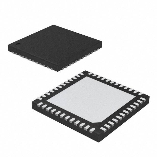
This 3.3V IC is available in a 7mm x 7mm, 48-pin TQFN
package and operates from -40°C to +85°C.
Applications
Ethernet Switch/Router
Fibre Channel SAN
Wireless Base Station
SONET Line Cards
Features
S Inputs
Crystal Interface: 18MHz to 33.5MHz
LVCMOS Input: 15MHz to 160MHz
Differential Input: 15MHz to 350MHz
S Outputs
LVCMOS Output: Up to 160MHz
LVPECL/LVDS Outputs: Up to 800MHz
S Three Individual Output Banks
Pin-Programmable Dividers
Pin-Programmable Output Interface
S Wide VCO Tuning Range (3.60GHz to 3.83GHz)
S Low Phase Jitter
0.34psRMS (12kHz to 20MHz)
0.14psRMS (1.875MHz to 20MHz)
S Excellent Power-Supply Noise Rejection
S -40NC to +85NC Operating Temperature Range
S +3.3V Supply
Ordering Information
Typical Application Circuits and Pin Configuration appear at
end of data sheet.
PART
TEMP RANGE
PIN-PACKAGE
MAX3637ETM+
-40NC to +85NC
48 TQFN-EP*
+Denotes a lead(Pb)-free/RoHS-compliant package.
*EP = Exposed pad.
Functional Diagram
LVPECL/LVDS
QA0
QA0
LVPECL/LVDS
MAX3637
QA1
QA1
LVPECL/LVDS
QA2
QA2
XOUT
LVPECL/LVDS
XO
QA3
XIN
LVPECL/LVDS
LVCMOS
CIN
QA3
QA4
PLL, DIVIDERS, MUXES
VCO
QA4
LVPECL/LVDS
QB0
QB0
LVPECL/LVDS
DIN
DIN
QB1
QB1
LVPECL/LVDS
QB2
QB2
LVPECL/LVDS
QC
QC
LVCMOS
QCC
________________________________________________________________ Maxim Integrated Products 1
For pricing, delivery, and ordering information, please contact Maxim Direct at 1-888-629-4642,
or visit Maxim’s website at www.maxim-ic.com.
MAX3637
General Description
�MAX3637
Low-Jitter, Wide Frequency Range,
Programmable Clock Generator with 10 Outputs
ABSOLUTE MAXIMUM RATINGS
Supply Voltage Range (VCC, VCCA, VCCQA,
VCCQB, VCCQC, VCCQCC).................................-0.3V to +4.0V
Voltage Range at CIN, IN_SEL, DM, DF[1:0],
DP, PLL_BP, DA[1:0], DB[1:0], DC[1:0],
QA_CTRL1, QA_CTRL2, QB_CTRL,
QC_CTRL, QCC, RES............................ -0.3V to (VCC + 0.3V)
Voltage Range at DIN, DIN......... (VCC - 2.35V) to (VCC - 0.35V)
Voltage Range at QA[4:0], QA[4:0], QB[2:0],
QB[2:0], QC, QC when LVDS Output.... -0.3V to (VCC + 0.3V)
Current into QA[4:0], QA[4:0], QB[2:0], QB[2:0],
QC, QC when LVPECL Output...................................... -56mA
Current into QCC.............................................................. Q50mA
Voltage Range at XIN............................................-0.3V to +1.2V
Voltage Range at XOUT..............................-0.3V to (VCC - 0.6V)
Continuous Power Dissipation (TA = +70NC)
48-Pin TQFN (derate 40mW/NC above +70NC)...........3200mW
Operating Junction Temperature Range.......... -55NC to +150NC
Storage Temperature Range............................. -65NC to +160NC
Stresses beyond those listed under “Absolute Maximum Ratings” may cause permanent damage to the device. These are stress ratings only, and functional
operation of the device at these or any other conditions beyond those indicated in the operational sections of the specifications is not implied. Exposure to absolute
maximum rating conditions for extended periods may affect device reliability.
ELECTRICAL CHARACTERISTICS
(VCC = +3.0V to +3.6V, TA = -40°C to +85°C. Typical values are at VCC = +3.3V, TA = +25°C, unless otherwise noted. Signal applied
to CIN or DIN/DIN only when selected as the reference clock.) (Note 1)
PARAMETER
Supply Current with PLL
Enabled (Note 2)
SYMBOL
ICC
Supply Current with PLL
Bypassed (Note 2)
TYP
MAX
Configured with LVPECL outputs
CONDITIONS
MIN
170
215
Configured with LVDS outputs
290
365
Configured with LVPECL outputs
110
Configured with LVDS outputs
230
UNITS
mA
mA
LVCMOS/LVTTL CONTROL INPUTS (IN_SEL, DM, DF[1:0], DA[1:0], DB[1:0], DC[1:0], PLL_BP, DP, QA_CTRL1,
QA_CTRL2, QB_CTRL, QC_CTRL)
Input High Voltage
VIH
Input Low Voltage
VIL
2.0
Input High Current
IIH
VIN = VCC
Input Low Current
IIL
VIN = 0V
V
0.8
V
80
FA
-80
FA
LVCMOS/LVTTL CLOCK INPUT (CIN)
Reference Clock Input
Frequency
fREF
Input Amplitude Range
Internally AC-coupled (Note 3)
Input High Current
IIH
Input Low Current
IIL
VIN = VCC
VIN = 0V
Reference Clock Input DutyCycle Distortion
15
160
MHz
1.2
3.6
VP-P
80
FA
-80
40
Input Capacitance
Input Differential Voltage Swing
VCMI
15
VCC 1.8
%
pF
350
VCC 1.3
MHz
V
150
1800
mVP-P
Single-Ended Voltage Range
VCC 2.0
VCC 0.7
V
Input Differential Impedance
80
120
I
Differential Input Capacitance
2
60
1.5
DIFFERENTIAL CLOCK INPUT (DIN, DIN) (Note 4)
Differential Input Frequency
fREF
Input Bias Voltage
FA
100
1.5
pF
�Low-Jitter, Wide Frequency Range,
Programmable Clock Generator with 10 Outputs
(VCC = +3.0V to +3.6V, TA = -40°C to +85°C. Typical values are at VCC = +3.3V, TA = +25°C, unless otherwise noted. Signal applied
to CIN or DIN/DIN only when selected as the reference clock.) (Note 1)
PARAMETER
SYMBOL
CONDITIONS
MIN
TYP
LVDS OUTPUTS (QA[4:0], QA[4:0], QB[2:0], QB[2:0], QC, QC) (Note 5)
Output Frequency
Output High Voltage
VOH
Output Low Voltage
VOL
0.925
Differential Output Voltage
|VOD|
250
Change in Magnitude
of Differential Output for
Complementary States
Output Offset Voltage
Change in Magnitude of
Output Offset Voltage for
Complementary States
1.125
D|VOS|
Differential Output Impedance
80
Output Current
Output Current When Disabled
Output Rise/Fall Time
Output Duty-Cycle Distortion
100
Short together
3
Short to ground
6
VQ__ = VQ__ = 0V to VCC
20% to 80%
10
PLL enabled
48
PLL bypassed (Note 6)
UNITS
800
MHz
1.475
V
V
D|VOD|
VOS
MAX
400
mV
25
mV
1.3
V
25
mV
140
I
mA
FA
160
240
50
52
50
LVPECL OUTPUTS (QA[4:0], QA[4:0], QB[2:0], QB[2:0], QC, QC) (Note 7)
Output Frequency
ps
%
800
MHz
VCC 0.98
VCC 0.83
V
Output High Voltage
VOH
VCC 1.13
Output Low Voltage
VOL
VCC 1.85
VCC 1.70
VCC 1.55
V
0.5
0.7
0.9
VP-P
Output-Voltage Swing
(Single-Ended)
Output Current When Disabled
VO = 0V to VCC
10
Output Rise/Fall Time
20% to 80%, differential load = 100I
140
240
50
52
Output Duty-Cycle Distortion
PLL enabled
48
PLL bypassed (Note 6)
FA
50
ps
%
LVCMOS/LVTTL OUTPUT (QCC)
Output Frequency
Output High Voltage
IOH = -12mA
Output Low Voltage
IOL = 12mA
Output Rise/Fall Time
20% to 80% (Note 8)
150
PLL enabled
42
Output Duty-Cycle Distortion
Output Impedance
PLL bypassed (Note 6)
2.6
160
MHz
VCC
V
0.4
V
400
850
ps
50
58
50
15
%
I
3
MAX3637
ELECTRICAL CHARACTERISTICS (continued)
�MAX3637
Low-Jitter, Wide Frequency Range,
Programmable Clock Generator with 10 Outputs
ELECTRICAL CHARACTERISTICS (continued)
(VCC = +3.0V to +3.6V, TA = -40°C to +85°C. Typical values are at VCC = +3.3V, TA = +25°C, unless otherwise noted. Signal applied
to CIN or DIN/DIN only when selected as the reference clock.) (Note 1)
PARAMETER
SYMBOL
CONDITIONS
MIN
TYP
MAX
UNITS
3750
3830
MHz
42
MHz
PLL SPECIFICATIONS
VCO Frequency Range
fVCO
3600
Phase-Frequency Detector
Compare Frequency
fPFD
15
PLL Jitter Transfer Bandwidth
Integrated Phase Jitter
RJ
25MHz crystal
input (Note 9)
0.34
1.875MHz to 20MHz
0.14
kHz
1.0
psRMS
25MHz LVCMOS or differential input
(Notes 9, 10)
0.34
Supply-Noise Induced Phase
Spur at LVPECL/LVDS Output
(Note 11)
-56
dBc
Supply-Noise Induced Phase
Spur at LVCMOS Output
(Note 11)
-45
dBc
Determinisitic Jitter Induced by
Power-Supply Noise
LVPECL or LVDS (Note 11)
6
psP-P
Nonharmonic and Subharmonic
Spurs
(Note 12)
-70
dBc
fOFFSET = 1kHz
-109
fOFFSET = 10kHz
-112
fOFFSET = 100kHz
-118
fOFFSET = 1MHz
-134
fOFFSET R 10MHz
-146
fOFFSET = 1kHz
-119
fOFFSET = 10kHz
-121
fOFFSET = 100kHz
-127
fOFFSET = 1MHz
-143
fOFFSET R 10MHz
-151
fOFFSET = 1kHz
-122
fOFFSET = 10kHz
-123
fOFFSET = 100kHz
-129
fOFFSET = 1MHz
-145
fOFFSET R 10MHz
-152
fOFFSET = 1kHz
-123
fOFFSET = 10kHz
-124
fOFFSET = 100kHz
-130
fOFFSET = 1MHz
-147
fOFFSET R 10MHz
-153
SSB Phase Noise at 622.08MHz
SSB Phase Noise at 212.5MHz
SSB Phase Noise at 156.25MHz
SSB Phase Noise at 125MHz
4
130
12kHz to 20MHz
dBc/
Hz
dBc/
Hz
dBc/
Hz
dBc/
Hz
�Low-Jitter, Wide Frequency Range,
Programmable Clock Generator with 10 Outputs
(VCC = +3.0V to +3.6V, TA = -40°C to +85°C. Typical values are at VCC = +3.3V, TA = +25°C, unless otherwise noted. Signal applied
to CIN or DIN/DIN only when selected as the reference clock.) (Note 1)
PARAMETER
SYMBOL
SSB Phase Noise at 62.5MHz
CONDITIONS
MIN
TYP
fOFFSET = 1kHz
-129
fOFFSET = 10kHz
-130
fOFFSET = 100kHz
-137
fOFFSET = 1MHz
-152
fOFFSET R 10MHz
-156
MAX
UNITS
dBc/
Hz
Note 1: A series resistor of up to 10.5I is allowed between VCC and VCCA for filtering supply noise when system power-supply
tolerance is VCC = 3.3V Q5%. See Figure 3.
Note 2: Measured with all outputs enabled and unloaded.
Note 3: CIN can be AC- or DC-coupled. See Figure 8. Input high voltage must be ≤ VCC + 0.3V.
Note 4: DIN can be AC- or DC-coupled. See Figure 10.
Note 5: Measured with 100I differential load.
Note 6: Measured with crystal input, or with 50% duty cycle LVCMOS or differential input.
Note 7: Measured with output termination of 50I to VCC - 2V or Thevenin equivalent.
Note 8: Measured with a series resistor of 33I to a load capacitance of 3.0pF. See Figure 1.
Note 9: Measured at 156.25MHz output.
Note 10: Measured using LVCMOS/LVTTL input with slew rate R 1.0V/ns, or differential input with slew rate R 0.5V/ns.
Note 11: Measured at 156.25MHz output with 200kHz, 50mVP-P sinusoidal signal on the supply using the crystal input and
the power-supply filter shown in Figure 3. See the Typical Operating Characteristics for other supply noise frequencies. Deterministic jitter is calculated from the measured power-supply-induced spurs. For more information, refer to
Application Note 4461: HFAN-04.5.5: Characterizing Power-Supply Noise Rejection in PLL Clock Synthesizers.
Note 12: Measured with all outputs enabled and all three banks at different frequencies.
LVCMOS
QCC
33Ω
499Ω
Z = 50Ω
OSCILLOSCOPE
0.1µF
Z = 50Ω
3pF
50Ω
MAX3637
Figure 1. LVCMOS Output Measurement Setup
5
MAX3637
ELECTRICAL CHARACTERISTICS (continued)
�Typical Operating Characteristics
(VCC = 3.3V, TA = +25NC, unless otherwise noted.)
PLL BYPASS, ALL OUTPUTS LOADED
250
PLL NORMAL, ALL OUTPUTS UNLOADED
200
150
400
PLL NORMAL
350
300
250
200
150
PLL BYPASS
400
300
150
100
50
10
35
60
0
85
QA[2:0] ENABLED
200
50
-15
QA[4:3] AND QA[2:0] ENABLED
250
50
-40
QA[4:3], QA[2:0], AND QB[2:0] ENABLED
350
100
PLL BYPASS, ALL OUTPUTS UNLOADED
QA[4:3], QA[2:0], QB[2:0],
QC, AND QCC ENABLED
450
100
0
ALL OUTPUTS DISABLED
0
-40
-15
10
35
60
85
-40
-15
10
35
60
85
TEMPERATURE (°C)
TEMPERATURE (°C)
TEMPERATURE (°C)
SUPPLY CURRENT vs. TEMPERATURE
(LVDS OUTPUTS)
DIFFERENTIAL OUTPUT AT 737.28MHz
(LVPECL)
DIFFERENTIAL OUTPUT AT 312.5MHz
(LVPECL)
QA[4:3], QA[2:0], QB[2:0],
QC, AND QCC ENABLED
300
250
QA[4:3], QA[2:0], AND QB[2:0] ENABLED
200
QA[4:3] AND QA[2:0] ENABLED
150
QA[2:0] ENABLED
100
MAX3637 toc06
MAX3637 toc04
MAX3637 toc05
350
SUPPLY CURRENT (mA)
500
SUPPLY CURRENT (mA)
350
300
450
SUPPLY CURRENT (mA)
400
SUPPLY CURRENT vs. TEMPERATURE
(LVPECL OUTPUTS, ALL LOADED)
MAX3637 toc02
PLL NORMAL, ALL OUTPUTS LOADED
450
500
MAX3637 toc01
500
SUPPLY CURRENT vs. TEMPERATURE
(LVDS OUTPUTS, ALL ENABLED)
MAX3637 toc03
SUPPLY CURRENT vs. TEMPERATURE
(LVPECL OUTPUTS, ALL ENABLED)
SUPPLY CURRENT (mA)
MAX3637
Low-Jitter, Wide Frequency Range,
Programmable Clock Generator with 10 Outputs
200mV/div
200mV/div
ALL OUTPUTS DISABLED
50
0
-40
-15
10
35
60
85
200ps/div
500ps/div
DIFFERENTIAL OUTPUT AT 156.25MHz
(LVPECL)
DIFFERENTIAL OUTPUT AT 156.25MHz
(LVDS)
QCC OUTPUT AT 125MHz
(LVCMOS)
MAX3637 toc07
MAX3637 toc08
TEMPERATURE (°C)
200mV/div
100mV/div
1ns/div
6
MAX3637 toc09
500mV/div
1ns/div
1ns/div
�Low-Jitter, Wide Frequency Range,
Programmable Clock Generator with 10 Outputs
OUTPUT SWING
vs. TEMPERATURE
LVPECL
1500
500
0
0
100
LVDS
1000
500
10
MAX3637 toc11
2000
LVPECL
0
-15
OUTPUT FREQUENCY (MHz)
LVPECL/LVDS
50.2
50.0
49.8
49.6
-90
-100
-110
-120
-130
-140
-110
-120
-130
-140
-150
85
1k
TEMPERATURE (°C)
100k
1M
10M
100M
1k
-100
-110
-120
-130
-90
-100
-110
-120
-130
-90
-110
-120
-130
-150
-150
-150
-160
-160
-160
100k
1M
10M
OUTPUT FREQUENCY (Hz)
100M
100M
-100
-140
10k
10M
-80
-140
1k
1M
PHASE JITTER = 0.36psRMS
INTEGRATED 12kHz TO 20MHz
-70
PHASE NOISE (dBc/Hz)
-90
100k
PHASE NOISE AT 125MHz
-60
MAX3637 toc17
-80
PHASE NOISE (dBc/Hz)
-80
PHASE JITTER = 0.34psRMS
INTEGRATED 12kHz TO 20MHz
-70
10k
OUTPUT FREQUENCY (Hz)
PHASE NOISE AT 156.25MHz
-60
MAX3637 toc16
PHASE JITTER = 0.31psRMS
INTEGRATED 12kHz TO 20MHz
-70
10k
OUTPUT FREQUENCY (Hz)
PHASE NOISE AT 212.5MHz
-60
85
-90
-160
60
60
-100
-160
35
35
-80
49.0
10
10
PHASE JITTER = 0.32psRMS
INTEGRATED 12kHz TO 20MHz
-70
-150
-15
-15
PHASE NOISE AT 312.5MHz
-60
49.2
-40
PHASE NOISE (dBc/Hz)
-40
TEMPERATURE (°C)
-80
LVCMOS
49.4
85
PHASE NOISE (dBc/Hz)
50.4
60
PHASE JITTER = 0.27psRMS
INTEGRATED 12kHz TO 20MHz
-70
PHASE NOISE (dBc/Hz)
50.6
35
PHASE NOISE AT 622.08MHz
-60
MAX3637 toc13
DUTY-CYCLE DISTORTION (%)
50.8
10
TEMPERATURE (°C)
DUTY-CYCLE DISTORTION vs. TEMPERATURE
51.0
LVDS
200
100
-40
1000
300
MAX3637 toc15
LVDS
1000
LVCMOS
MAX3637 toc18
1500
2500
LVCMOS
400
RISE/FALL TIME (ps)
LVPECL
2000
3000
OUTPUT SWING (mVP-P)
LVCMOS
2500
500
MAX3637 toc14
3000
OUTPUT SWING (mVP-P)
3500
MAX3637 toc10
3500
RISE/FALL TIME vs. TEMPERATURE
(20% TO 80%)
MAX3637 toc12
OUTPUT SWING
vs. OUTPUT FREQUENCY
-140
1k
10k
100k
1M
10M
OUTPUT FREQUENCY (Hz)
100M
1k
10k
100k
1M
10M
100M
OUTPUT FREQUENCY (Hz)
7
MAX3637
Typical Operating Characteristics (continued)
(VCC = 3.3V, TA = +25NC, unless otherwise noted.)
�Typical Operating Characteristics (continued)
(VCC = 3.3V, TA = +25NC, unless otherwise noted.)
-90
-100
-110
-120
-130
-140
-150
OUTPUT FREQUENCY = 156.25MHz
0.55
0.50
0.45
LVCMOS
0.40
0.35
0.30
LVPECL
0.25
0.20
-160
1k
10k
100k
1M
10M
-15
-40
100M
10
35
60
85
OUTPUT FREQUENCY (Hz)
TEMPERATURE (°C)
JITTER TRANSFER
SPURS INDUCED BY POWER-SUPPLY NOISE
vs. NOISE FREQUENCY
0
MAX3637 toc21
5
0
-5
fC = 156.25MHz, NOISE = 50mVP-P
-10
SPUR AMPLITUDE (dBc)
-10
-15
-20
-25
-30
-35
-20
LVCMOS
-30
-40
-50
-60
LVDS
-70
-40
LVPECL
-80
-45
-50
-90
1k
10k
100k
1M
10M
100
10
JITTER FREQUENCY (Hz)
NOISE FREQUENCY (kHz)
40
fC = 156.25MHz, NOISE = 50mVP-P
DETERMINISTIC JITTER (psP-P)
35
30
MAX3637 toc23
DETERMINISTIC JITTER INDUCED BY POWERSUPPLY NOISE vs. NOISE FREQUENCY
LVCMOS
25
20
LVPECL
15
10
5
LVDS
0
10
100
NOISE FREQUENCY (kHz)
8
LVDS
MAX3637 toc22
PHASE NOISE (dBc/Hz)
-80
INTEGRATED PHASE JITTER (psRMS)
PHASE JITTER = 0.40psRMS
INTEGRATED 12kHz TO 20MHz
-70
0.60
MAX3637 toc19
-60
MAX3637 toc20
INTEGRATED PHASE JITTER (12kHz TO 20MHz)
vs. TEMPERATURE
PHASE NOISE AT 62.5MHz
JITTER TRANSFER (dB)
MAX3637
Low-Jitter, Wide Frequency Range,
Programmable Clock Generator with 10 Outputs
1000
1000
�Low-Jitter, Wide Frequency Range,
Programmable Clock Generator with 10 Outputs
PIN
NAME
MAX3637
Pin Description
FUNCTION
1
DM
LVCMOS/LVTTL Input. Three-level control for input divider M. See Table 3.
2
XIN
Crystal Oscillator Input
3
XOUT
4
VCC
Crystal Oscillator Output
Core Power Supply. Connect to +3.3V.
5
IN_SEL
LVCMOS/LVTTL Input. Three-level control for input mux. See Table 1.
6
PLL_BP
LVCMOS/LVTTL Input. Three-level control for PLL bypass mode. See Table 2.
7, 8
DF1, DF0
LVCMOS/LVTTL Inputs. Three-level controls for feedback divider F. See Table 4.
9
QC_CTRL
LVCMOS/LVTTL Input. Three-level control input for C-bank output interface. See Table 10.
10
VCCA
Power Supply for Internal Voltage-Controlled Oscillators (VCOs). See Figure 3.
11
RES
Reserved. Connect to GND for normal operation.
12
DP
LVCMOS/LVTTL Input. Three-level control for prescale divider P. See Table 7.
13, 14
DB1, DB0
LVCMOS/LVTTL Inputs. Three-level controls for output divider B. See Table 5.
15, 16
DA1, DA0
LVCMOS/LVTTL Inputs. Three-level controls for output divider A. See Table 5.
17, 18
DC1, DC0
LVCMOS/LVTTL Inputs. Three-level controls for output divider C. See Table 6.
19
QA_CTRL2
LVCMOS/LVTTL Input. Three-level control for QA[4:3] output interface. See Table 8.
20
VCCQCC
21
QCC
22, 23
QC, QC
VCCQC
C-Bank Differential Output. Configured as LVPECL or LVDS with the QC_CTRL pin.
24
25, 36
VCCQA
Power Supply for A-Bank Differential Outputs. Connect to +3.3V.
26, 27
QA4, QA4
A-Bank Differential Output. Configured as LVPECL or LVDS with the QA_CTRL2 pin.
28, 29
QA3, QA3
A-Bank Differential Output. Configured as LVPECL or LVDS with the QA_CTRL2 pin.
30, 31
QA2, QA2
A-Bank Differential Output. Configured as LVPECL or LVDS with the QA_CTRL1 pin.
32, 33
QA1, QA1
A-Bank Differential Output. Configured as LVPECL or LVDS with the QA_CTRL1 pin.
34, 35
A-Bank Differential Output. Configured as LVPECL or LVDS with the QA_CTRL1 pin.
37
QA0, QA0
VCCQB
38, 39
QB0, QB0
B-Bank Differential Output. Configured as LVPECL or LVDS with the QB_CTRL pin.
40, 41
QB1, QB1
B-Bank Differential Output. Configured as LVPECL or LVDS with the QB_CTRL pin.
42, 43
B-Bank Differential Output. Configured as LVPECL or LVDS with the QB_CTRL pin.
44
QB2, QB2
QA_CTRL1
45
QB_CTRL
LVCMOS/LVTTL Input. Three-level control for B-bank output interface. See Table 9.
46, 47
DIN, DIN
Differential Clock Input. Operates up to 350MHz. This input can accept DC-coupled LVPECL signals, and is internally biased to accept AC-coupled LVDS, CML, and LVPECL signals.
48
CIN
LVCMOS Clock Input. Operates up to 160MHz.
—
EP
Exposed Pad. Connect to supply ground for proper electrical and thermal performance.
Power Supply for QCC Output. Connect to +3.3V.
C-Bank LVCMOS Clock Output
Power Supply for C-Bank Differential Output. Connect to +3.3V.
Power Supply for B-Bank Differential Outputs. Connect to +3.3V.
LVCMOS/LVTTL Input. Three-level control for QA[2:0] output interface. See Table 8.
9
�MAX3637
Low-Jitter, Wide Frequency Range,
Programmable Clock Generator with 10 Outputs
Detailed Description
banks of clock outputs. See Figure 2. The output banks
include nine pin-programmable LVDS/LVPECL output
buffers and one LVCMOS output buffer. The frequency,
enabling, and output interface of each output bank can
be individually programmed. In addition the A-bank is
split into two banks with programmable enabling and
The MAX3637 is a low-jitter clock generator designed to
operate over a wide range of frequencies. It consists of
a selectable reference clock (on-chip crystal oscillator,
LVCMOS input, or differential input), PLL with on-chip
VCO, pin-programmable dividers and muxes, and three
IN_SEL
VCC
DM
DP
VCCA
DA[1:0]
PLL_BP
VCCQA
QA_CTRL1
2
QA0
QA0
XOUT
CRYSTAL
OSCILLATOR
QA1
1
0
XIN
fREF
LVCMOS
CIN
NC
÷M
PFD
VCO
CP
fVCO
÷P
÷A
fQA
QA1
QA2
0/NC
QA2
fPFD
15MHz TO 42MHz
3600MHz TO 3830MHz
QA3
QA3
DIN
DIN
QA4
÷F
QA4
1
QA_CTRL2
VCCQB
QB_CTRL
QB0
MAX3637
QB0
QB1
1
÷B
fQB
QB1
QB2
0/NC
QB2
DIVIDER A: 1, 2, 3, 4, 5, 6, 8, 10, 12
DIVIDER B: 1, 2, 3, 4, 5, 6, 8, 10, 12
DIVIDER C: 2, 3, 4, 5, 6, 8, 10, 12, 25
DIVIDER F: 16, 20, 24, 25, 28, 30, 32, 40, 48
DIVIDER M: 1, 4, 5
DIVIDER P: 5, 6, 8
QC_CTRL
QC
1/NC
÷C
2
EP
Figure 2. Detailed Functional Diagram
10
DF[1:0]
2
DB[1:0]
fQC
QC
0
QCC
2
DC[1:0]
VCCQC
VCCQCC
�Low-Jitter, Wide Frequency Range,
Programmable Clock Generator with 10 Outputs
Crystal Oscillator
The on-chip crystal oscillator provides the low-frequency
reference clock for the PLL. This oscillator requires an
external crystal connected between XIN and XOUT.
See the Crystal Selection and Layout section for more
information. The XIN and XOUT pins can be left open if
not used.
LVCMOS Clock Input
An LVCMOS-compatible clock source can be connected
to CIN to serve as the PLL reference clock. The input is
internally biased to allow AC- or DC-coupling (see the
Applications Information section). It is designed to operate from 15MHz to 160MHz. No signal should be applied
to CIN if not used.
(see the Applications Information section). No signal
should be applied to DIN if not used.
Phase-Locked Loop (PLL)
The PLL takes the signal from the crystal oscillator,
LVCMOS clock input, or differential clock input and synthesizes a low-jitter, high-frequency clock. The PLL contains a phase-frequency detector (PFD), a charge pump
(CP), and a low phase noise VCO with a wide 3.60GHz to
3.83GHz frequency range. The high-frequency VCO output is divided by prescale divider P, then is connected to
the PFD input through a feedback divider. The PFD compares the reference frequency to the divided-down VCO
output and generates a control signal that keeps the
VCO locked to the reference clock. The high-frequency
VCO/P output clock is sent to the output dividers. To
minimize noise-induced jitter, the VCO supply (VCCA) is
isolated from the core logic and output buffer supplies.
Differential Clock Input
A differential clock source can be connected to DIN
to serve as the PLL reference clock. This input operates from 15MHz to 350MHz and contains an internal
100ω differential termination. This input can accept
DC-coupled LVPECL signals, and is internally biased to
accept AC-coupled LVDS, CML, and LVPECL signals
Dividers and Muxes
The dividers and muxes are set with three-level control
inputs. Leakage in the NC case must be less than 1µA.
Divider settings and routing information are given in
Tables 1 to 7. See Table 11 for example divider configurations used in various applications.
Table 1. PLL Input
IN_SEL
INPUT
0
Crystal Input. XO circuit is disabled when not selected.
1
Differential Input. No signal should be applied to DIN if not selected.
NC
LVCMOS Input. No signal should be applied to CIN if not selected.
Table 2. PLL Bypass
PLL_BP
PLL OPERATION
0
PLL Enabled for Normal Operation. All outputs from the A, B, and C banks are derived from the VCO.
1
PLL Bypassed. Selected input passes directly to the outputs. The VCO is disabled to minimize power consumption and intermodulation spurs. Used for system testing or clock distribution.
NC
The outputs from A-bank and B-bank are derived from the VCO, but the C-bank outputs are directly driven from
the input signal for purposes of daisy chaining.
11
MAX3637
output interface. A PLL bypass mode is also available for
system testing or clock distribution.
�MAX3637
Low-Jitter, Wide Frequency Range,
Programmable Clock Generator with 10 Outputs
Table 3. Input Divider M
Table 7. Prescale Divider P
DM
M DIVIDER RATIO
DP
P DIVIDER RATIO
0
÷1
0
÷5
1
÷5
1
÷6
NC
÷4
NC
÷8
Note: When the on-chip XO is selected (IN_SEL = 0), the setting DM = 0 is required.
Table 4. PLL Feedback Divider F
QA_CTRL1
QA[2:0] OUTPUT
0
QA[2:0] = LVDS
DF1
DF0
F DIVIDER RATIO
1
QA[2:0] = LVPECL
0
0
÷25
NC
QA[2:0] disabled to high impedance
0
1
÷20
QA_CTRL2
QA[4:3] OUTPUT
1
0
÷16
0
QA[4:3] = LVDS
1
1
÷32
1
QA[4:3] = LVPECL
1
NC
÷24
NC
QA[4:3] disabled to high impedance
NC
1
÷30
0
NC
÷40
NC
0
÷48
NC
NC
÷28
Table 5. Output Divider A, B
DA1/DB1
DA0/DB0
A, B DIVIDER RATIO
0
0
÷2
0
1
÷3
1
0
÷4
1
1
÷5
1
NC
÷6
NC
1
÷8
0
NC
÷10
NC
0
÷12
NC
NC
÷1
Table 6. Output Divider C
12
Table 8. A-Bank Output Interface
DC1
DC0
C DIVIDER RATIO
0
0
÷2
0
1
÷3
1
0
÷4
1
1
÷5
1
NC
÷6
NC
1
÷8
0
NC
÷10
NC
0
÷12
NC
NC
÷25
Table 9. B-Bank Output Interface
QB_CTRL
QB[2:0] OUTPUT
0
QB[2:0] = LVDS
1
QB[2:0] = LVPECL
NC
QB[2:0] disabled to high impedance
Table 10. C-Bank Output Interface
QC_CTRL
QC AND QCC OUTPUT
0
QC = LVDS, QCC = LVCMOS
1
QC = LVPECL, QCC = LVCMOS
NC
QC and QCC disabled to high impedance
LVDS/LVPECL Clock Outputs
The differential clock outputs (QA[4:0], QB[2:0], QC)
operate up to 800MHz and have a pin-programmable
LVDS/LVPECL output interface. See Tables 8 to 10.
When configured as LVDS, the buffers are designed
to drive transmission lines with a 100ω differential termination. When configured as LVPECL, the buffers are
designed to drive transmission lines terminated with 50ω
to VCC - 2V. Unused output banks can be disabled to
high impedance and unused outputs can be left open.
LVCMOS Clock Output
The LVCMOS clock output operates up to 160MHz and is
designed to drive a single-ended high-impedance load.
If unused, this output can be left open or the C-bank can
be disabled to high impedance.
�Low-Jitter, Wide Frequency Range,
Programmable Clock Generator with 10 Outputs
The prescale divider P is set by DP as given in Table 7.
In addition, the reference clock frequency and input
divider M must also be selected so the PFD compare
frequency (fPFD) falls within the specified range of
15MHz to 42MHz. If applicable, the higher fPFD should
be selected for optimal jitter performance.
Applications Information
Output Frequency Configuration
The MAX3637 output frequencies (fQA, fQB, fQC) are
functions of the reference frequency (fREF) and the pinprogrammable dividers (A, B, C, F, M). The relationships
can be expressed as:
f
F
fQA = REF ×
M
A
(1)
f
F
fQB = REF ×
M
B
(2)
f
F
fQC = REF ×
M
C
(3)
The frequency ranges for the selected reference clocks
are 18MHz to 33.5MHz for the crystal oscillator input,
15MHz to 160MHz for the LVCMOS input, and 15MHz to
350MHz for the differential input. The available dividers
are given in Tables 3 to 6.
For a given reference frequency fREF, the input divider
M, the PLL feedback divider F, and VCO prescale divider
P must be configured so the VCO frequency (fVCO) falls
within the specified ranges. Invalid PLL configuration
leads to VCO frequencies beyond the specified ranges
and can result in loss of lock. An expression for the VCO
frequency along with the specified ranges is given by:
f
fVCO = REF × F × P
M
(4)
3600MHz ≤ fVCO ≤ 3830MHz (5)
f
f
fPFD = REF = VCO
M
P ×F
(6)
15MHz ≤ fPFD ≤ 42MHz (7)
Note that the reference clock frequency is not limited by
the fPFD range when the PLL is in bypass mode.
Example Frequency Configuration
The following is an example of how to find divider ratios
for a valid PLL configuration, given a requirement of
input and output frequencies.
1) S
� elect input and output frequencies for system clocking.
fREF = 25MHz
fQA = 312.5MHz
fQB = 156.25MHz
fQC = 125MHz
2) F
� ind the input divider M for a valid PFD compare
frequency. Using Table 3 and equations (6) and (7),
it is determined that M = ÷1 is the only valid option.
3) F
� ind the feedback divider F and prescale divider P for
a valid fVCO. Using Tables 4 and 7 along with equations (4) and (5), it is determined that F = ÷25 and P
= ÷6 results in fVCO = 3750MHz, which is within the
valid range of the low VCO.
4) F
� ind the output dividers A, B, C for the required output
frequencies. Using Tables 5 and 6 and equations (1),
(2), and (3), it is determined that A = ÷2 gives fQA =
312.5MHz, B = ÷4 gives fQB = 156.25MHz, and C =
÷5 gives fQC = 125MHz.
Table 11 provides input and output frequencies along
with valid divider ratios for a variety of applications.
13
MAX3637
Internal Reset
During power-on, a power-on reset (POR) signal is generated to synchronize all dividers. A reset signal is also
generated if any control pin is changed. Outputs within a
bank are phase aligned, but outputs bank-to-bank may
not be phase aligned.
�MAX3637
Low-Jitter, Wide Frequency Range,
Programmable Clock Generator with 10 Outputs
Table 11. Reference Frequencies and Divider Ratios for Various Applications
fREF
(MHz)
INPUT
DIVIDER
(M)
PLL
FEEDBACK
DIVIDER
(F)
15.36
1
48
30.72
1
24
61.44
4
48
VCO
FREQUENCY
(MHz)
3686.4
VCO
PRESCALE
DIVIDER
(P)
OUTPUT
DIVIDER
(A, B, C)
OUTPUT
FREQUENCY
(MHz)
5
1
737.28
5
2
368.64
5
3
245.76
5
4
184.32
5
6
122.88
5
8
92.16
5
12
61.44
122.88
4
24
15.36
1
40
6
1
614.4
19.2
1
32
6
2
307.2
30.72
1
20
6
3
204.8
38.4
1
16
6
4
153.6
61.44
4
40
6
5
122.88
122.88
4
20
6
6
102.4
153.6
4
16
6
8
76.8
6
12
51.3
25/31.25/
62.5/125/
156.25
25/20/40/
25/20
6
1
625
1/1/4/5/5
6
2
312.5
6
4
156.25
6
5
125
6
10
62.5
6
20
31.25
6
25
25
5
3
250
5
4
187.5
5
5
150
5
6
125
5
12
62.5
6
2
318.75
6
3
212.5
6
4
159.375
6
6
106.25
6
12
53.125
3686.4
3750
26.04166
25/31.25/
125
26.5625
1
1/1/4
1
24
30/24/24
24
3750
3825
19.44
1
32
6
1
622.08
38.88
1
16
6
2
311.04
6
4
155.52
6
8
77.76
155.52
4
16
3732.48
cdma2000 is a registered trademark of the Telecommunications Industry Association.
WiMAX is a trademark of WiMAX Forum.
14
APPLICATIONS
Wireless Base Station:
WCDMA, cdma2000®,
LTE, TD_SCDMA,
WiMAX™, GSM
Ethernet
FC-SAN
SONET/SDH, STM-N
�Low-Jitter, Wide Frequency Range,
Programmable Clock Generator with 10 Outputs
+3.3V ±5%
VCC
0.1µF
10.5Ω
MAX3637
VCCA
0.1µF
10µF
Figure 3. Power-Supply Filter
Ground Connection
The 48-pin TQFN package features an exposed pad
(EP), which provides a low resistance thermal path for
heat removal from the IC and also the electrical ground.
For proper operation, the EP must be connected to the
circuit board ground plane with multiple vias.
Crystal Selection and Layout
The MAX3637 features an integrated on-chip crystal
oscillator to minimize system implementation cost. The
crystal oscillator is designed to drive a fundamental
mode, AT-cut crystal resonator. See Table 12 for recommended crystal specifications. See Figure 4 for the crystal equivalent circuit and Figure 5 for the recommended
external capacitor connections. The crystal, trace, and
two external capacitors should be placed on the board
as close as possible to the XIN and XOUT pins to reduce
crosstalk of active signals into the oscillator.
The total
load capacitance for the crystal is a combination of
external and on-chip capacitance. The layout shown
in Figure 6 gives approximately 1.7pF of trace plus
footprint capacitance per side of the crystal. Note the
ground plane is removed under the crystal to minimize
capacitance. There is approximately 2.5pF of on-chip
capacitance between XIN and XOUT. With an external
27pF capacitor connected to XIN and a 33pF external
capacitor connected to XOUT, the total load capacitance
for the crystal is approximately 18pF. The XIN and XOUT
pins can be left open if not used.
Table 12. Crystal Selection Parameters
PARAMETER
Crystal Oscillation Frequency
SYMBOL
MIN
fOSC
18
TYP
MAX
UNITS
25
33.5
MHz
Shunt Capacitance
C0
2.0
7.0
pF
Load Capacitance
CL
18
Equivalent Series Resistance (ESR)
RS
10
pF
Maximum Crystal Drive Level
XTAL
50
I
200
FW
27pF
XIN
CRYSTAL
(CL = 18pF)
C0
RS
LS
Figure 4. Crystal Equivalent Circuit
CS
MAX3637
XOUT
33pF
Figure 5. Crystal, Capacitor Connections
15
MAX3637
Power-Supply Filtering
The MAX3637 is a mixed analog/digital IC. The PLL
contains analog circuitry susceptible to random noise.
To take full advantage of on-board filtering and noise
attenuation, in addition to excellent on-chip power-supply rejection, this part provides a separate power-supply
pin, VCCA, for the VCO circuitry. Figure 3 illustrates the
recommended power-supply filter network for VCCA.
The purpose of this design technique is to ensure clean
input power supply to the VCO circuitry and to improve
the overall immunity to power-supply noise. This network requires that the power supply is +3.3V ±5%.
Decoupling capacitors should be used on all other supply pins for best performance. All supply connections
should be driven from the same source.
�Low-Jitter, Wide Frequency Range,
Programmable Clock Generator with 10 Outputs
MAX3637
Interfacing with LVCMOS Input
The equivalent LVCMOS input circuit for CIN is given in
Figure 7. This input is internally biased to allow AC- or
DC-coupling, and has 180kI input impedance. See
Figure 8 for the interface circuit. No signal should be
applied to CIN if not used.
Interfacing with Differential Input
The equivalent input circuit for DIN is given in Figure 9.
This input operates up to 350MHz and contains an
internal 100I differential termination as well as a 35I
common-mode termination. The common-mode termination ensures good signal integrity when connected to a
source with large common-mode signals. The input can
accept DC-coupled LVPECL signals, and is internally
biased to accept AC-coupled LVDS, CML, and LVPECL
signals (Figure 10). No signal should be applied to DIN
if not used.
Figure 6. Crystal Layout
1.4V
VCC
VBIAS
VCC
180kΩ
CIN
VCC
ESD
STRUCTURES
ESD
STRUCTURES
DIN
Figure 7. Equivalent CIN Circuit
50Ω
20kΩ
10Ω
VCC
VCC - 1.3V
16pF
50Ω
DC-COUPLED
MAX3637
DIN
CIN
XO
ESD
STRUCTURES
Figure 9. Equivalent DIN Circuit
AC-COUPLED
MAX3637
0.1µF
XO
Figure 8. Interface to CIN
16
CIN
20kΩ
�Low-Jitter, Wide Frequency Range,
Programmable Clock Generator with 10 Outputs
MAX3637
150Ω
+3.3V
+3.3V
DIN
Z = 50Ω
LVPECL
100Ω
LVPECL
DIN
Z = 50Ω
The equivalent LVPECL output circuit is given in Figure
11. These outputs are designed to drive a pair of 50ω
transmission lines terminated with 50ω to VTT = VCC - 2V.
If a separate termination voltage (VTT) is not available,
other terminations methods can be used, as shown in
Figure 12. For more information on LVPECL terminations
and how to interface with other logic families, refer to
Application Note 291: HFAN-01.0: Introduction to LVDS,
PECL, and CML.
150Ω
VCC_ _
LVPECL SOURCE DRIVING MAX3637
DIFFERENTIAL INPUT AC-COUPLED
+3.3V
MAX3637
150Ω
0.1µF
Z = 50Ω
LVPECL
0.1µF
Z = 50Ω
+3.3V
DIN
100Ω
Q_ _
LVPECL
Q_ _
DIN
150Ω
ESD
STRUCTURES
LVDS OR CML SOURCE DRIVING MAX3637
DIFFERENTIAL INPUT AC-COUPLED
Figure 11. Equivalent LVPECL Output Circuit
MAX3637
VDD
0.1µF
Z = 50Ω
LVDS OR
CML
0.1µF
Z = 50Ω
+3.3V
DIN
100Ω
LVPECL
DIN
Figure 10. Interfacing to DIN
17
MAX3637
Interfacing with LVPECL Outputs
LVPECL SOURCE DRIVING MAX3637
DIFFERENTIAL INPUT DC-COUPLED
�MAX3637
Low-Jitter, Wide Frequency Range,
Programmable Clock Generator with 10 Outputs
DC-COUPLED LVPECL DRIVING THEVENIN EQUIVALENT TERMINATION
+3.3V
+3.3V
+3.3V
130Ω
MAX3637
Q_ _
+3.3V
130Ω
HIGH IMPEDANCE
WITH/WITHOUT
DC BIAS
Z = 50Ω
LVPECL
LVPECL
Q_ _
Z = 50Ω
82Ω
82Ω
AC-COUPLED LVPECL DRIVING INTERNAL 100Ω DIFFERENTIAL TERMINATION
+3.3V
VDD
150Ω
MAX3637
Q_ _
ON-CHIP
TERMINATION
WITH DC BIAS
0.1µF
Z = 50Ω
LVPECL
100Ω
0.1µF
Q_ _
LVPECL
Z = 50Ω
150Ω
AC-COUPLED LVPECL DRIVING EXTERNAL 50Ω WITH COMMON-MODE TERMINATION
+3.3V
VDD
150Ω
MAX3637
Q_ _
0.1µF
HIGH IMPEDANCE
WITH
DC BIAS
Z = 50Ω
LVPECL
LVPECL
0.1µF
Q_ _
Z = 50Ω
150Ω
50Ω
0.1µF
Figure 12. Interface to LVPECL Outputs
18
50Ω
�Low-Jitter, Wide Frequency Range,
Programmable Clock Generator with 10 Outputs
Interfacing with LVDS Outputs
VCC_ _
50Ω
Q_ _
The equivalent LVDS output circuit is given in Figure 13.
These outputs provide 100ω differential output impedance designed to drive a 100ω differential transmission
line terminated with a 100ω differential load. Example
interface circuits are shown in Figure 14. For more information on LVDS terminations and how to interface with
other logic families, refer to Application Note 291: HFAN01.0: Introduction to LVDS, PECL, and CML.
50Ω
Q_ _
ESD
STRUCTURES
Interfacing with LVCMOS Output
The equivalent LVCMOS output circuit is given in Figure
15. This output provides 15ω output impedance and
is designed to drive a high-impedance load. A series
resistor of 33ω is recommended at the LVCMOS output
before the transmission line. An example interface circuit
is shown in Figure 16.
Figure 13. Equivalent LVDS Output Circuit
VCCQCC
DC-COUPLED LVDS OUTPUT DRIVING LVDS INPUT
+3.3V
+3.3V
10Ω
MAX3637
Q_ _
Z = 50Ω
LVDS
QCC
LVDS*
Q_ _
10Ω
Z = 50Ω
ESD
STRUCTURES
AC-COUPLED LVDS OUTPUT DRIVING LVDS INPUT
+3.3V
MAX3637
Figure 15. Equivalent LVCMOS Output Circuit
VDD
Q_ _
LVDS
Q_ _
0.1µF
Z = 50Ω
LVDS*
0.1µF
LVCMOS
QCC
33Ω
Z = 50Ω
HIGH
IMPEDANCE
Z = 50Ω
MAX3637
*100Ω DIFFERENTIAL INPUT IMPEDANCE ASSUMED.
Figure 16. Interface to LVCMOS Output
Figure 14. Interface to LVDS Outputs
19
MAX3637
VREG
�Layout Considerations
• T
� he crystal, trace, and two external capacitors should
be placed on the board as close as possible to the
XIN and XOUT pins to reduce crosstalk of active signals into the oscillator.
The inputs and outputs are the most critical paths for
the MAX3637; great care should be taken to minimize
discontinuities on the transmission lines. Here are some
suggestions for maximizing the performance of the
MAX3637:
• M
� aintain 100ω differential (or 50ω single-ended) transmission line impedance into and out of the part.
• A
� n uninterrupted ground plane should be positioned
beneath the clock outputs. The ground plane under
the crystal should be removed to minimize capacitance.
• P
� rovide space between differential output pairs to
reduce crosstalk, especially if the outputs are operating at different frequencies.
• U
� se multilayer boards with an uninterrupted ground
plane to minimize EMI and crosstalk.
• S
� upply decoupling capacitors should be placed close
to the supply pins, preferably on the same side of the
board as the MAX3637.
Refer to the MAX3637 evaluation kit for more information.
Chip Information
• T
� ake care to isolate input traces from the MAX3637
outputs.
PROCESS: BiCMOS
QA0
QA1
QA1
QA2
QA2
QA3
QA3
QA4
QA4
VCCQA
36
QA0
TOP VIEW
VCCQA
Pin Configuration
35
34
33
32
31
30
29
28
27
26
25
VCCQB
37
24
VCCQC
QB0
38
23
QC
QB0
39
22
QC
QB1
40
21
QCC
QB1
41
20
VCCQCC
MAX3637
QB2
42
19
QA_CTRL2
QB2
43
18
DC0
QA_CTRL1
44
17
DC1
QB_CTRL
45
16
DA0
DIN
46
15
DA1
DIN
47
14
DB0
CIN
48
13
DB1
*EP
5
6
7
8
9
10
11
12
DF1
DF0
QC_CTRL
VCCA
RES
DP
XOUT
4
PLL_BP
3
VCC
2
IN_SEL
1
XIN
+
DM
MAX3637
Low-Jitter, Wide Frequency Range,
Programmable Clock Generator with 10 Outputs
THIN QFN
(7mm × 7mm × 0.8mm)
*THE EXPOSED PAD OF THE QFN PACKAGE MUST BE SOLDERED TO GROUND FOR PROPER THERMAL AND ELECTRICAL OPERATION.
20
�Low-Jitter, Wide Frequency Range,
Programmable Clock Generator with 10 Outputs
+3.3V
10.5Ω
10µF
0.1µF
0.1µF
VCCA
27pF
VCC
0.1µF
VCCQA
VCCQB
XIN
0.1µF
VCCQC
0.1µF
0.1µF
VCCQCC
150Ω
312.5MHz
LVPECL
Z = 50Ω
QA[4:0]
0.1µF
25MHz
XOUT
NC
CIN
NC
DIN
NC
DIN
100Ω
0.1µF
Z = 50Ω
QA[4:0]
33pF
ASIC WITH LVPECL
TERMINATION
150Ω
156.25MHz
LVDS
Z = 50Ω
IN_SEL
MAX3637
PLL_BP
QB[2:0]
ASIC WITH LVDS
TERMINATION
100Ω
DM
DF1
QB[2:0]
Z = 50Ω
QC
125MHz
LVDS
Z = 50Ω
DF0
DA1
+3.3V
DA0
DB1
ASIC WITH LVDS
TERMINATION
100Ω
DB0
DC1
Z = 50Ω
QC
DC0
DP
RES
33Ω
QA_CTRL1
QCC
QA_CTRL2
125MHz
LVCMOS
Z = 50Ω
ASIC WITH LVCMOS
TERMINATION
HIGH
IMPEDANCE
QB_CTRL
QC_CTRL
EP
21
MAX3637
Typical Application Circuits
�Low-Jitter, Wide Frequency Range,
Programmable Clock Generator with 10 Outputs
MAX3637
Typical Application Circuits (continued)
CLOCK GENERATOR FOR ETHERNET AND SYSTEM CLOCKING
XIN
QA[4:0]
312.5MHz
LVPECL OR LVDS
BACKPLANE
TRANSCEIVER
QB[2:0]
156.25MHz
LVPECL OR LVDS
10GbE PHY
25MHz
LVCMOS
ASIC
QA[4:0]
125MHz
LVPECL OR LVDS
1GbE PHY
QB[2:0]
100MHz
LVPECL OR LVDS
PCIe
QC
66.67MHz
LVPECL OR LVDS
NETWORK
PROCESSOR
QCC
66.67MHz
LVCMOS
FPGA
25MHz
XOUT
MAX3637
QCC
QC
25MHz LVPECL
DIN
MAX3638
FREQUENCY TRANSLATOR FOR BASE STATION
30.72MHz
122.88MHz
LVPECL OR LVDS
CPRI
SerDes
QB[2:0]
153.6MHz
LVPECL OR LVDS
SRIO
QC
30.72MHz
LVPECL OR LVDS
FPGA
QCC
30.72MHz
LVCMOS
FPGA
DIN
MAX3637
22
QA[4:0]
�Low-Jitter, Wide Frequency Range,
Programmable Clock Generator with 10 Outputs
CLOCK GENERATOR FOR FIBRE CHANNEL
XIN
QA[4:0]
212.5MHz
LVPECL OR LVDS
8G PHY
QB[2:0]
106.25MHz
LVPECL OR LVDS
4G PHY
QC
106.25MHz
LVPECL OR LVDS
ASIC
26.5625MHz
XOUT
MAX3637
QCC
NC
FREQUENCY SYNTHESIZER FOR SONET LINE CARD
19.44MHz
QA[4:0]
622.08MHz
LVPECL OR LVDS
OC-192 PHY
QB[2:0]
155.52MHz
LVPECL OR LVDS
OC-48 PHY
QC
155.52MHz
LVPECL OR LVDS
ASIC
QCC
38.88MHz
LVCMOS
ASIC
DIN
MAX3637
Package Information
For the latest package outline information and land patterns, go to www.maxim-ic.com/packages. Note that a “+”, “#”, or “-” in the
package code indicates RoHS status only. Package drawings may show a different suffix character, but the drawing
pertains to the package regardless of RoHS status.
PACKAGE TYPE
PACKAGE CODE
DOCUMENT NO.
48 TQFN-EP
T4877+4
21-0144
Maxim cannot assume responsibility for use of any circuitry other than circuitry entirely embodied in a Maxim product. No circuit patent licenses are implied.
Maxim reserves the right to change the circuitry and specifications without notice at any time.
Maxim Integrated Products, 120 San Gabriel Drive, Sunnyvale, CA 94086 408-737-7600
© 2009
Maxim Integrated Products
23
Maxim is a registered trademark of Maxim Integrated Products, Inc.
MAX3637
Typical Application Circuits (continued)
�


 工商网监
湘ICP备2023018690号
工商网监
湘ICP备2023018690号
