MCP111/112
Micropower Voltage Detector
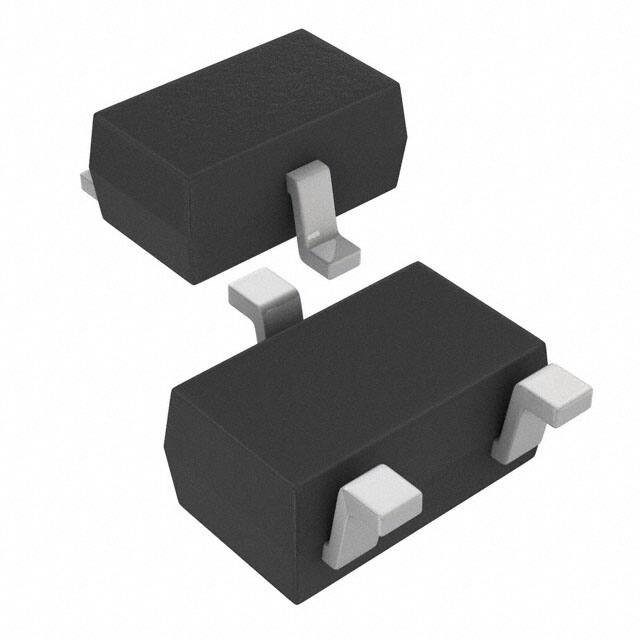
Package Types
• Ultra-Low Supply Current: 1.75 µA (Max.)
• Precision Monitoring Options Of:
- 1.90V, 2.32V, 2.63V, 2.90V, 2.93V, 3.08V,
4.38V and 4.63V
• Resets Microcontroller in a Power-Loss Event
• Active-Low VOUT Pin:
- MCP111 Active-Low, Open-Drain
- MCP112 Active-Low, Push-Pull
• Available in SOT23-3, TO-92, SC-70 and
SOT-89-3 Packages
• Temperature Range:
- Extended: -40°C to +125°C
(except MCP1XX-195)
- Industrial: -40°C to +85°C (MCP1XX-195 Only)
• Pb-Free Devices
3-Pin SOT23-3/SC-70
VOUT 1
VSS 2
3-Pin SOT-89
VDD
MCP111/112
Features
3 VDD
MCP111/112
1
2
3
VOUT VDD VSS
3-Pin TO-92
VOUT
VDD VSS
Applications
Block Diagram
• Critical Microcontroller and Microprocessor
Power-Monitoring Applications
• Computers
• Intelligent Instruments
• Portable Battery-Powered Equipment
VDD
Comparator
+
General Description
Output
Driver
–
The MCP111/112 are voltage-detecting devices
designed to keep a microcontroller in reset until the
system voltage has stabilized at the appropriate level
for reliable system operation. These devices also
operate as protection from brown-out conditions when
the system supply voltage drops below the specified
threshold voltage level. Eight different trip voltages are
available.
VOUT
Band Gap
Reference
VSS
DEVICE FEATURES
Output
SOT-23/SC70
Package Pin Out
(Pin # 1, 2, 3)
Type
Pull-up Resistor
Reset Delay
(typ.)
MCP111
Open-drain
External
No
VOUT, VSS, VDD
Device
Comment
MCP112
Push-pull
No
No
VOUT, VSS, VDD
MCP102
Push-pull
No
120 ms
RST, VDD, VSS
See MCP102/103/121/131 Data Sheet
(DS20001906)
MCP103
Push-pull
No
120 ms
VSS, RST, VDD
See MCP102/103/121/131 Data Sheet
(DS20001906)
MCP121
Open-drain
External
120 ms
RST, VDD, VSS
See MCP102/103/121/131 Data Sheet
(DS20001906)
MCP131
Open-Drain
Internal (~95 k)
120 ms
RST, VDD, VSS
See MCP102/103/121/131 Data Sheet
(DS20001906)
2004-2016 Microchip Technology Inc.
DS20001889F-page 1
�MCP111/112
1.0
ELECTRICAL
CHARACTERISTICS
† Notice: Stresses above those listed under “Maximum
Ratings” may cause permanent damage to the device. This is
a stress rating only and functional operation of the device at
those or any other conditions above those indicated in the
operational listings of this specification is not implied.
Exposure to maximum rating conditions for extended periods
may affect device reliability.
Absolute Maximum Ratings†
VDD...................................................................................7.0V
Input current (VDD) .......................................................10 mA
Output current (RST) ....................................................10 mA
Rated Rise Time of VDD .............................................100V/µs
All inputs and outputs (except RST) w.r.t. VSS
.............................................................. -0.6V to (VDD + 1.0V)
RST output w.r.t. VSS ....................................... -0.6V to 13.5V
Storage temperature .....................................65°C to + 150°C
Ambient temp. with power applied ...............-40°C to + 125°C
Maximum Junction temp. with power applied ............... 150°C
ESD protection on all pins 2 kV
DC CHARACTERISTICS
Electrical Specifications: Unless otherwise indicated, all limits are specified for VDD = 1V to 5.5V, RPU = 100 k (only MCP111),
TA = -40°C to +125°C.
Symbol
Min.
Typ.
Max.
Units
Operating Voltage Range
Parameters
VDD
1.0
—
5.5
V
Specified VDD Value to VOUT low
VDD
1.0
—
Operating Current
IDD
—
5.5V applied 100s,
current into pin limited to
2 mA, +25°C operation
recommended
Note 3, Note 4
Open-drain Output Leakage Current
(MCP111 only)
IOD
—
0.1
—
µA
Note 1:
2:
3:
4:
Trip point is ±1.5% from typical value.
Trip point is ±2.5% from typical value.
This specification allows this device to be used in PIC® microcontroller applications that require the In-Circuit Serial
Programming™ (ICSP™) feature (see device-specific programming specifications for voltage requirements). This
specification DOES NOT allow a continuous high voltage to be present on the open-drain output pin (VOUT). The total
time that the VOUT pin can be above the maximum device operational voltage (5.5V) is 100 sec. Current into the VOUT
pin should be limited to 2 mA. It is recommended that the device operational temperature be maintained between 0°C
to 70°C (+25°C preferred). For additional information, please refer to Figure 2-28.
This parameter is established by characterization and is not 100% tested.
2004-2016 Microchip Technology Inc.
DS20001889F-page 3
�MCP111/112
VTRIP
1V
VDD
tRPU
tRPD
VOH
1V
VOL
VOUT
tRT
FIGURE 1-1:
Timing Diagram.
AC CHARACTERISTICS
Electrical Specifications: Unless otherwise indicated, all limits are specified for VDD = 1V to 5.5V, RPU = 100 k
(only MCP111), TA = -40°C to +125°C.
Parameters
Symbol
Min.
Typ.
Max.
Units
VDD Detect to VOUT Inactive
tRPU
—
90
—
µs
Figure 1-1 and CL = 50 pF
(Note 1)
VDD Detect to VOUT Active
tRPD
—
130
—
µs
VDD ramped from VTRIP(MAX) +
250 mV down to VTRIP(MIN) –
250 mV, per Figure 1-1,
CL = 50 pF (Note 1)
tRT
—
5
—
µs
For VOUT 10% to 90% of final
value per Figure 1-1, CL = 50 pF
(Note 1)
VOUT Rise Time After VOUT Active
Note 1:
Conditions
These parameters are for design guidance only and are not 100% tested.
TEMPERATURE CHARACTERISTICS
Electrical Specifications: Unless otherwise noted, all limits are specified for VDD = 1V to 5.5V, RPU = 100 k
(MCP111 only), TA = -40°C to +125°C.
Parameters
Symbol
Min.
Typ.
Max.
Units
Conditions
Specified Temperature Range
TA
-40
—
+85
°C
MCP1XX-195
Specified Temperature Range
TA
-40
—
+125
°C
Except MCP1XX-195
Maximum Junction Temperature
TJ
—
—
+150
°C
Storage Temperature Range
TA
-65
—
+150
°C
Temperature Ranges
Package Thermal Resistances
Thermal Resistance, 3L-SOT23
JA
—
336
—
°C/W
Thermal Resistance, 3L-SC-70
JA
—
340
—
°C/W
Thermal Resistance, 3L-TO-92
JA
—
131.9
—
°C/W
Thermal Resistance, 3L-SOT-89
JA
—
110
—
°C/W
DS20001889F-page 4
2004-2016 Microchip Technology Inc.
�MCP111/112
2.0
TYPICAL PERFORMANCE CURVES
Note:
The graphs and tables provided following this note are a statistical summary based on a limited number of
samples and are provided for informational purposes only. The performance characteristics listed herein
are not tested or guaranteed. In some graphs or tables, the data presented may be outside the specified
operating range (e.g., outside specified power supply range) and therefore outside the warranted range.
Note: Unless otherwise indicated, all limits are specified for VDD = 1V to 5.5V, RPU = 100 k (only MCP111;
see Figure 4-1), TA = -40°C to +125°C.
1.6
1.6
MCP111-195
5.5V
5.0V
1.4
1.4
1.2
1.2
4.0V
1
0.8
IDD (uA)
IDD (uA)
MCP111-195
2.8V
2.1V
1.7V
0.6
0.4
+85°C
0.8
0.6
-40°C
0.4
1.0V
0.2
+125°C
1
+25°C
0.2
0
140
120
100
80
60
40
20
0
-20
-40
0
1.0
2.0
3.0
FIGURE 2-1:
(MCP111-195).
FIGURE 2-4:
IDD vs. Temperature
1
5.0V
0.8
4.0V
0.6
2.8V
1.7V
IDD vs. VDD (MCP111-195).
1.2
2.1V
1
+125°C
0.8
+85°C
0.6
-40°C
0.4
0.2
1.0V
0.2
0
+25°C
140
120
100
80
60
40
20
0
-20
-40
0
1.0
2.0
3.0
FIGURE 2-5:
IDD vs. Temperature
FIGURE 2-2:
(MCP112-300).
4.0
5.0
6.0
VDD (V)
Temperature (°C)
IDD vs. VDD (MCP112-300).
1.6
MCP112-475
1.4
5.5V
MCP112-475
2.1V
2.8V
1.7V
IDD (uA)
1.2
4.0V
5.0V
1
0.8
+125°C
0.6
+85°C
0.4
-40°C
0.2
1.0V
+25°C
140
120
100
80
60
40
20
0
-20
0
-40
IDD (uA)
6.0
MCP112-300
1.4
0.4
1
0.9
0.8
0.7
0.6
0.5
0.4
0.3
0.2
0.1
0
5.0
1.6
5.5V
MCP112-300
IDD (uA)
IDD (uA)
1.2
4.0
VDD (V)
Temperature (°C)
1.0
IDD vs. Temperature
2004-2016 Microchip Technology Inc.
3.0
4.0
5.0
6.0
VDD (V)
Temperature (°C)
FIGURE 2-3:
(MCP112-475).
2.0
FIGURE 2-6:
IDD vs. VDD (MCP112-475).
DS20001889F-page 5
�MCP111/112
Note: Unless otherwise indicated, all limits are specified for VDD = 1V to 5.5V, RPU = 100 k (only MCP111;
see Figure 4-1), TA = -40°C to +125°C.
0.050
0.045
0.040
0.035
0.030
0.025
0.020
0.015
0.010
0.005
0.000
140
0.100
VTRIP, V increasing
MCP111-195
max temp is
+85°C
VTRIP, V decreasing
-60
-10
40
90
MCP111-195
VDD = 1.7V
0.080
VOL (V)
VHYS, Hysteresis
Hyst (V)
VTRIP (V)
0.120
1.950
1.945
1.940
1.935
1.930
1.925
1.920
1.915
1.910
1.905
1.900
1.895
+125°C
0.060
+85°C
0.040
-40°C
0.020
+25°C
0.000
0.00
0.25
Temperature (°C)
0.50
0.75
1.00
IOL (mA)
FIGURE 2-10:
VOL vs. IOL
(MCP111-195 @ VDD = 1.7V).
FIGURE 2-7:
VTRIP and VHYST vs.
Temperature (MCP111-195).
0.080
3.020
VTRIP (V)
3.000
VHYS, Hysteresis
2.980
MCP112-300
2.960
2.940
2.920
VTRIP, V decreasing
2.900
-60
-10
40
90
0.100
0.098
0.096
0.094
0.092
0.090
0.088
0.086
0.084
0.082
140
0.070
MCP112-300
VDD = 2.7V
0.060
VOL (V)
VTRIP, V increasing
Hyst (V)
3.040
0.050
+125°C
0.040
+85°C
0.030
0.020
-40°C
+25°C
0.010
0.000
0.00
0.25
Temperature (°C)
0.050
0.180
VTRIP, V increasing
0.170
0.160
0.150
0.140
MCP112-475
0.130
0.120
20
60
100
0.100
140
Temperature (°C)
FIGURE 2-9:
VTRIP and VHYST vs.
Temperature (MCP112-475).
DS20001889F-page 6
1.00
MCP112-475
VDD = 4.4V
+125°C
0.030
0.020
+85°C
-40°C
0.010
+25°C
0.110
VTRIP, V decreasing
-20
0.040
VOL (V)
VHYS, Hysteresis
-60
0.75
FIGURE 2-11:
VOL vs. IOL
(MCP112-300 @ VDD = 2.7V).
Hyst (V)
VTRIP (V)
FIGURE 2-8:
VTRIP and VHYST vs.
Temperature (MCP112-300).
4.800
4.780
4.760
4.740
4.720
4.700
4.680
4.660
4.640
4.620
4.600
4.580
0.50
IOL (mA)
0.000
0.00
0.25
0.50
0.75
1.00
IOL (mA)
FIGURE 2-12:
VOL vs. IOL
(MCP112-475 @ VDD = 4.4V).
2004-2016 Microchip Technology Inc.
�MCP111/112
Note: Unless otherwise indicated, all limits are specified for VDD = 1V to 5.5V, RPU = 100 k (only MCP111;
see Figure 4-1), TA = -40°C to +125°C.
0.120
MCP111-195
VDD = 1.7 V
0.100
VOH (V)
IOL = 0.50 mA
0.060
0.040
MCP112-300
VDD = 3.1V
3.100
IOL = 0.75 mA
0.080
VOL (V)
3.150
IOL = 1.00 mA
-40 °C
3.050
+25 °C
3.000
IOL = 0.25 mA
+85 °C
2.950
0.020
IOL = 0.00 mA
+125 °C
0.000
-40
0
40
80
2.900
0.00
120
0.25
Temperature (°C)
0.080
4.820
MCP112-300
VDD = 2.7V
4.800
IOL = 0.50 mA
0.030
VOH (V)
VOL (V)
4.780
IOL = 0.75 mA
0.050
0.040
IOL = 0.25 mA
0.020
0.010
80
-40 °C
4.740
+85 °C
4.700
+125 °C
0.000
40
+25 °C
4.760
4.720
IOL = 0.00 mA
0
4.680
0.00
120
0.25
Temperature (°C)
0.030
IOL = 0.50 mA
0.020
IOL = 0.25 mA
0.010
IOL = 0.00 mA
0.000
40
80
120
Transient Duration (µs)
VOL (V)
IOL = 0.75 mA
0
500
400
1
10
MCP111-195
MCP112-300
300
200
MCP112-475
100
0
0.001
FIGURE 2-15:
VOL vs. Temperature
(MCP112-475 @ VDD = 4.4V).
0.01
0.1
VTRIP(min) - VDD
Temperature (°C)
2004-2016 Microchip Technology Inc.
1.00
600
0.040
-40
0.75
FIGURE 2-17:
VOH vs. IOH
(MCP112-475 @ VDD = 4.8V).
IOL = 1.00 mA
MCP112-475
VDD = 4.4V
0.50
IOL (mA)
FIGURE 2-14:
VOL vs. Temperature
(MCP112-300 @ VDD = 2.7V).
0.050
1.00
MCP112-475
VDD = 4.8V
IOL = 1.00 mA
0.060
-40
0.75
FIGURE 2-16:
VOH vs. IOH
(MCP112-300 @ VDD = 3.1V).
FIGURE 2-13:
VOL vs. Temperature
(MCP111-195 @ VDD = 1.7V).
0.070
0.50
IOL (mA)
FIGURE 2-18:
(25 °C).
Typical Transient Response
DS20001889F-page 7
�MCP111/112
Note: Unless otherwise indicated, all limits are specified for VDD = 1V to 5.5V, RPU = 100 k (only MCP111;
see Figure 4-1), TA = -40°C to +125°C.
400
350
300
350
VDD decreasing from:
VTRIP(max) + 0.25V to VTRIP(min) - 0.25V
200
150
tRPU (µs)
300
250
tRPD (µs)
MCP111-195
MCP111-195
VDD decreasing from:
5V - 1.7V
100
200
150
VDD increasing from:
0V - 2.8V
100
VDD decreasing from:
5V - 0V
50
VDD increasing from:
0V - 2.1V
250
50
VDD increasing
from: 0V - 5.5V
0
0
-40
-15
10
35
60
85
-40
110
-15
10
Temperature (°C)
FIGURE 2-19:
(MCP111-195).
tRPD vs. Temperature
FIGURE 2-22:
(MCP111-195).
VDD decreasing from:
VTRIP(max) + 0.25V to VTRIP(min) - 0.25V
110
MCP112-300
100
100
tRPU (µs)
tRPD (µs)
85
tRPU vs. Temperature
VDD increasing from:
0V - 3.1V
120
120
VDD decreasing from:
5V - 2.7V
80
60
VDD increasing from:
0V - 3.3V
80
60
VDD increasing from:
0V - 4.0V
40
40
VDD decreasing from:
5V - 0V
20
0
VDD increasing from:
0V - 5.5V
0
-40
-15
10
35
60
85
110
-40
-15
Temperature (°C)
FIGURE 2-20:
(MCP112-300).
10
35
60
85
110
Temperature (°C)
tRPD vs. Temperature
FIGURE 2-23:
(MCP112-300).
tRPU vs. Temperature
250
250
MCP112-475
MCP112-475
VDD increasing from:
0V - 4.9V
200
tRPU (µs)
VDD decreasing from:
5V - 4.4V
200
tRPD (µs)
60
140
MCP112-300
140
150
100
35
Temperature (°C)
160
20
VDD increasing
from: 0V - 4.0V
VDD decreasing from:
VTRIP(max) + 0.25V to VTRIP(min) - 0.25V
150
VDD increasing from:
0V - 5.0V
100
VDD increasing from:
0V - 5.5V
50
50
VDD decreasing from:
5V - 0V
0
0
-40
-15
FIGURE 2-21:
(MCP112-475).
DS20001889F-page 8
10
35
60
Temperature (°C)
85
110
tRPD vs. Temperature
-40
-15
10
35
60
85
110
Temperature (°C)
FIGURE 2-24:
(MCP112-475).
tRPU vs. Temperature
2004-2016 Microchip Technology Inc.
�MCP111/112
Note: Unless otherwise indicated, all limits are specified for VDD = 1V to 5.5V, RPU = 100 k (only MCP111;
see Figure 4-1), TA = -40°C to +125°C.
0.1500
60
0.1400
VDD increasing from:
0V - 2.1V
45
VDD increasing from:
0V - 5.5V
40
VDD increasing
from: 0V - 4.0V
35
0.1200
VDD increasing from:
0V - 4.9V
0.1100
VDD increasing from:
0V - 5.5V
0.1000
30
VDD increasing from:
0V - 2.8V
25
0.0900
20
VDD increasing from:
0V - 4.8V
0.0800
-40
-15
10
35
60
85
110
-40
-15
10
Temperature (°C)
0.4
0.35
0.3
FIGURE 2-27:
(MCP112-475).
tRT vs. Temperature
VDD increasing from:
0V - 3.1V
VDD increasing from:
0V - 3.3V
0.25
0.2
VDD increasing from:
0V - 5.5V
0.15
VDD increasing from:
0V - 4.0V
0.1
0.05
MCP112-300
0
-40
-15
10
35
60
85
Temperature (°C)
FIGURE 2-26:
(MCP112-300).
tRT vs. Temperature
2004-2016 Microchip Technology Inc.
35
60
85
110
Temperature (°C)
110
tRT vs. Temperature
1.E-02
10m
1.E-03
1m
1.E-04
100µ
1.E-05
10µ
1.E-06
1µ
1.E-07
100n
1.E-08
10n
1.E-09
1n
1.E-10
100p
1.E-11
10p
1.E-12
1p
1.E-13
100f
Open-Drain Leakage (A)
FIGURE 2-25:
(MCP111-195).
tRT (µs)
VDD increasing from:
0V - 5.0V
0.1300
tRT (µs)
50
tRT (µs)
MCP112-475
MCP111-195
55
125°C
25°C
- 40°C
0
1
2
3
4
5
6
7
8
9 10 11 12 13 14
Pull-Up Voltage (V)
FIGURE 2-28:
Open-Drain Leakage
Current vs. Voltage Applied to VOUT Pin
(MCP111-195).
DS20001889F-page 9
�MCP111/112
3.0
PIN DESCRIPTION
The descriptions of the pins are listed in Table 3-1.
TABLE 3-1:
PIN FUNCTION TABLE
Pin Number
Symbol
SOT-23-3
SC-70
SOT-89-3
T0-92
1
1
1
VOUT
Function
Output State
VDD Falling:
H = VDD > VTRIP
L = VDD < VTRIP
VDD Rising:
H = VDD > VTRIP + VHYS
L = VDD < VTRIP + VHYS
2
3
3
VSS
Ground reference
3
2
2
VDD
Positive power supply
—
4
—
VDD
Positive power supply
DS20001889F-page 10
2004-2016 Microchip Technology Inc.
�MCP111/112
4.0
APPLICATION INFORMATION
4.1
For many of today’s microcontroller applications, care
must be taken to prevent low-power conditions that can
cause many different system problems. The most
common causes is a brown-out condition, where the
system supply drops below the operating level momentarily. The second most common cause is when a slowly
decaying power supply causes the microcontroller to
begin executing instructions without sufficient voltage to
sustain SRAM, thus producing indeterminate results.
Figure 4-1 shows a typical application circuit.
VTRIP Operation
The voltage trip point (VTRIP) is determined on the falling
edge of VDD. The actual voltage trip point (VTRIPAC) will
be between the minimum trip point (VTRIPMIN) and the
maximum trip point (VTRIPMAX). There is a hysteresis on
this trip point to remove any “jitter” that would occur on
the VOUT pin when the device VDD is at the trip point.
Figure 4-2 shows the state of the VOUT pin as
determined by the VDD voltage. The VTRIP specification
is for falling VDD voltages. When the VDD voltage is
rising, the VOUT pin will not be driven high until VDD is at
VTRIP + VHYS.
VDD
0.1
µF
3
VDD
VDD
RPU
MCP11X
(1)
VOUT
1
VSS
PIC®
Microcontroller
MCLR
(Reset Input)
GND
2
Note 1: RPU may be required with the MCP111
due to the open-drain output. Resistor
RPU is not required with the MCP112.
FIGURE 4-1:
VDD
Typical Application Circuit.
VTRIPAC + VHYSAC
VTRIPMAX
VTRIPAC
VTRIPMIN
VTRIPAC
1V
VOUT
< 1 V is outside the
device specifications
FIGURE 4-2:
4.2
VOUT Operation as Determined by the VTRIP and VHYS.
Negative Going VDD Transients
The minimum pulse width (time) required to cause a
reset may be an important criteria in the implementation of a Power-on Reset (POR) circuit. This time is
referred to as transient duration, defined as the amount
of time needed for these supervisory devices to
respond to a drop in VDD. The transient duration time is
dependent on the magnitude of VTRIP – VDD. Generally
speaking, the transient duration decreases with
increases in VTRIP – VDD.
2004-2016 Microchip Technology Inc.
Figure 4-3 shows a typical transient duration vs. reset
comparator overdrive for which the MCP111/112 will
not generate a reset pulse. It shows that the farther
below the trip point the transient pulse goes, the
duration of the pulse required to cause a reset gets
shorter. Figure 2-18 shows the transient response
characteristics for the MCP111/112.
A 0.1 µF bypass capacitor, mounted as close as
possible to the VDD pin, provides additional transient
immunity (refer to Figure 4-1).
DS20001889F-page 11
�MCP111/112
4.3
Supply Voltage
5V
0V
VTRIP(MAX)
VTRIP(MIN)
VTRIP(MIN) - VDD
tTRANS
Time (µs)
Effect of Temperature on Time-Out
Period (tRPU)
The time-out period (tRPU) determines how long the
device remains in the reset condition. This is affected
by both VDD and temperature. The graph shown in
Figures 2-22, 2-23 and 2-24 show the typical response
for different VDD values and temperatures.
Using in PIC® Microcontroller
ICSP™ Applications (MCP111
only)
4.4
FIGURE 4-3:
Example of Typical
Transient Duration Waveform.
Figure 4-4 shows the typical application circuit for using
the MCP111 for voltage supervisory function when the
PIC microcontroller will be programmed via the In-Circuit Serial Programming™ (ICSP) feature. Additional
information is available in TB087, “Using Voltage
Supervisors with PIC® Microcontroller Systems which
Implement
In-Circuit
Serial
Programming™”,
DS91087.
Note:
It is recommended that the current into the
RST pin be current limited by a 1 k
resistor.
VDD/VPP
0.1 µF
RPU
VDD
MCP111
RST
VSS
1 k
VDD
PIC®
MCU
MCLR
(reset input)
(Active-Low)
VSS
FIGURE 4-4:
Typical Application Circuit
for PIC® Microcontroller with the ICSP™ feature.
DS20001889F-page 12
2004-2016 Microchip Technology Inc.
�MCP111/112
5.0
PACKAGING INFORMATION
5.1
Package Marking Information
3-Lead TO-92
Example:
XXXXXX
XXXXXX
XXXXXX
YWWNNN
Device
Code
MCP111-240E/TO
240E
MCP111-270E/TO
270E
MCP111-290E/TO
290E
MCP111-300E/TO
300E
MCP111-315E/TO
315E
MCP111-450E/TO
450E
MCP111-475E/TO
475E
MCP111-195I/TO
195I
Example:
3-Lead SOT-23
Device
XXNN
Legend: XX...X
Y
WW
NNN
e3
*
Note:
MCP111
240E
TO^^
e3
626256
Code
MCP111T-195I/TT
MPNN
MCP111T-240ETT
MQNN
MCP111T-270E/TT
MGNN
MCP111T-290E/TT
NHNN
MCP111T-300E/TT
MJNN
MCP111T-315E/TT
MKNN
MCP111T-450E/TT
MLNN
MCP111T-475E/TT
MMNN
MCP112T-195I/TT
MRNN
MCP112T-240ETT
MSNN
MCP112T-270E/TT
MANN
MCP112T-290E/TT
MBNN
MCP112T-300E/TT
MCNN
MCP112T-315E/TT
MDNN
MCP112T-450E/TT
MENN
MCP112T-475E/TT
MFNN
MP25
Customer-specific information
Year code (last digit of calendar year)
Week code (week of January 1 is week ‘01’)
Alphanumeric traceability code
Pb-free JEDEC designator for Matte Tin (Sn)
This package is Pb-free. The Pb-free JEDEC designator ( e3 )
can be found on the outer packaging for this package.
In the event the full Microchip part number cannot be marked on one line, it will
be carried over to the next line, thus limiting the number of available
characters for customer-specific information.
2004-2016 Microchip Technology Inc.
DS20001889F-page 13
�MCP111/112
Package Marking Information (Continued)
3-Lead SC-70
Example:
Device
Code
MCP111T-195I/LB
EPNN
MCP111T-240E/LB
EQNN
MCP111T-270E/LB
EGNN
MCP111T-290E/LB
EHNN
MCP111T-300E/LB
EJNN
MCP111T-315E/LB
EKNN
MCP111T-450E/LB
ELNN
MCP111T-475E/LB
EMNN
MCP112T-195I/LB
ERNN
MCP112T-240E/LB
ESNN
MCP112T-270E/LB
EANN
MCP112T-290E/LB
EBNN
MCP112T-300E/LB
ECNN
MCP112T-315E/LB
EDNN
MCP112T-450E/LB
EENN
MCP112T-475E/LB
EFNN
3-Lead SOT-89
Example:
Device
MCP111T-195I/MB
NNN
DS20001889F-page 14
EP25
Code
MP
MCP111T-240EMB
MQ
MCP111T-270E/MB
MG
MCP111T-290E/MB
NH
MCP111T-300E/MB
MJ
MCP111T-315E/MB
MK
MCP111T-450E/MB
ML
MCP111T-475E/MB
MM
MCP112T-195I/MB
MR
MCP112T-240EMB
MS
MCP112T-270E/MB
MA
MCP112T-290E/MB
MB
MCP112T-300E/MB
MC
MCP112T-315E/MB
MD
MCP112T-450E/MB
ME
MCP112T-475E/MB
MF
MP1626
256
2004-2016 Microchip Technology Inc.
�MCP111/112
��/HDG�3ODVWLF�7UDQVLVWRU�2XWOLQH��72��>72���@
1RWH�
)RU�WKH�PRVW�FXUUHQW�SDFNDJH�GUDZLQJV��SOHDVH�VHH�WKH�0LFURFKLS�3DFNDJLQJ�6SHFLILFDWLRQ�ORFDWHG�DW�
KWWS���ZZZ�PLFURFKLS�FRP�SDFNDJLQJ
E
A
N
1
L
1 2
3
b
e
c
D
R
8QLWV
'LPHQVLRQ�/LPLWV
1XPEHU�RI�3LQV
,1&+(6
0,1
1
0$;
�
3LWFK
H
%RWWRP�WR�3DFNDJH�)ODW
'
����
�����%6&
����
2YHUDOO�:LGWK
(
����
����
2YHUDOO�/HQJWK
$
����
����
0ROGHG�3DFNDJH�5DGLXV
5
����
����
7LS�WR�6HDWLQJ�3ODQH
/
����
±
/HDG�7KLFNQHVV
F
����
����
/HDG�:LGWK
E
����
����
1RWHV�
�� 'LPHQVLRQV�$�DQG�(�GR�QRW�LQFOXGH�PROG�IODVK�RU�SURWUXVLRQV��0ROG�IODVK�RU�SURWUXVLRQV�VKDOO�QRW�H[FHHG�������SHU�VLGH�
�� 'LPHQVLRQLQJ�DQG�WROHUDQFLQJ�SHU�$60(�627���@
1RWH�
)RU�WKH�PRVW�FXUUHQW�SDFNDJH�GUDZLQJV��SOHDVH�VHH�WKH�0LFURFKLS�3DFNDJLQJ�6SHFLILFDWLRQ�ORFDWHG�DW�
KWWS���ZZZ�PLFURFKLS�FRP�SDFNDJLQJ
b
N
E
E1
2
1
e
e1
D
c
A
φ
A2
A1
L
8QLWV
'LPHQVLRQ�/LPLWV
1XPEHU�RI�3LQV
0,//,0(7(56
0,1
120
0$;
1
�
/HDG�3LWFK
H
�����%6&
2XWVLGH�/HDG�3LWFK
H�
2YHUDOO�+HLJKW
$
����
±
0ROGHG�3DFNDJH�7KLFNQHVV
$�
����
����
����
6WDQGRII
$�
����
±
����
2YHUDOO�:LGWK
(
����
±
����
0ROGHG�3DFNDJH�:LGWK
(�
����
����
����
2YHUDOO�/HQJWK
'
����
����
����
)RRW�/HQJWK
/
����
����
����
)RRW�$QJOH
�
�
±
��
/HDG�7KLFNQHVV
F
����
±
����
�����%6&
����
/HDG�:LGWK
E
����
±
����
1RWHV�
�� 'LPHQVLRQV�'�DQG�(��GR�QRW�LQFOXGH�PROG�IODVK�RU�SURWUXVLRQV��0ROG�IODVK�RU�SURWUXVLRQV�VKDOO�QRW�H[FHHG������PP�SHU�VLGH�
�� 'LPHQVLRQLQJ�DQG�WROHUDQFLQJ�SHU�$60(�