MCP1415/16
Tiny 1.5A, High-Speed Power MOSFET Driver
Features
General Description
• High Peak Output Current: 1.5A (typical)
• Wide Input Supply Voltage Operating Range:
- 4.5V to 18V
• Low Shoot-Through/Cross-Conduction Current in
Output Stage
• High Capacitive Load Drive Capability:
- 470 pF in 13 ns (typical)
- 1000 pF in 18 ns (typical)
• Short Delay Times: 44 ns (tD1), 47 ns (MCP1415
tD2), 54 ns (MCP1416 tD2) (typical)
• Low Supply Current:
- With Logic ‘1’ Input - 0.65 mA (typical)
- With Logic ‘0’ Input - 0.1 mA (typical)
• Latch-Up Protected: Withstands 500 mA Reverse
Current
• Logic Input Withstands Negative Swing up to 5V
• Space-Saving 5L SOT-23 Package
The MCP1415/16 devices are high-speed, dual
MOSFET drivers that are capable of providing up to
1.5A of peak current while operating from a single 4.5V
to 18V supply. The inverting or non-inverting single
channel output is directly controlled from either TTL or
CMOS (3V to 18V) logic. These devices also feature
low shoot-through current, matched rise and fall time,
and short propagation delays which make them ideal
for high switching frequency applications. They provide
low enough impedances in both the ‘On’ and ‘Off’
states to ensure the intended state of the MOSFET is
not affected, even by large transients.
Applications
•
•
•
•
•
These devices are highly latch-up resistant under any
condition within their power and voltage ratings. They
are not subject to damage when noise spiking (up to
5V, of either polarity) occurs on the Ground pin. They
can accept up to 500 mA of reverse current being
forced back into their outputs without damage or logic
upset. All terminals are fully protected against
electrostatic discharge (ESD) up to 2.0 kV (HBM) and
300V (MM).
Switch Mode Power Supplies
Pulse Transformer Drive
Line Drivers
Level Translator
Motor and Solenoid Drive
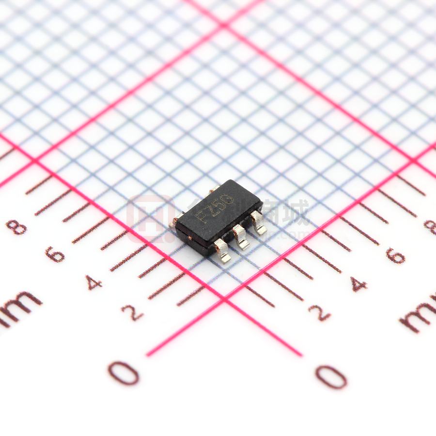
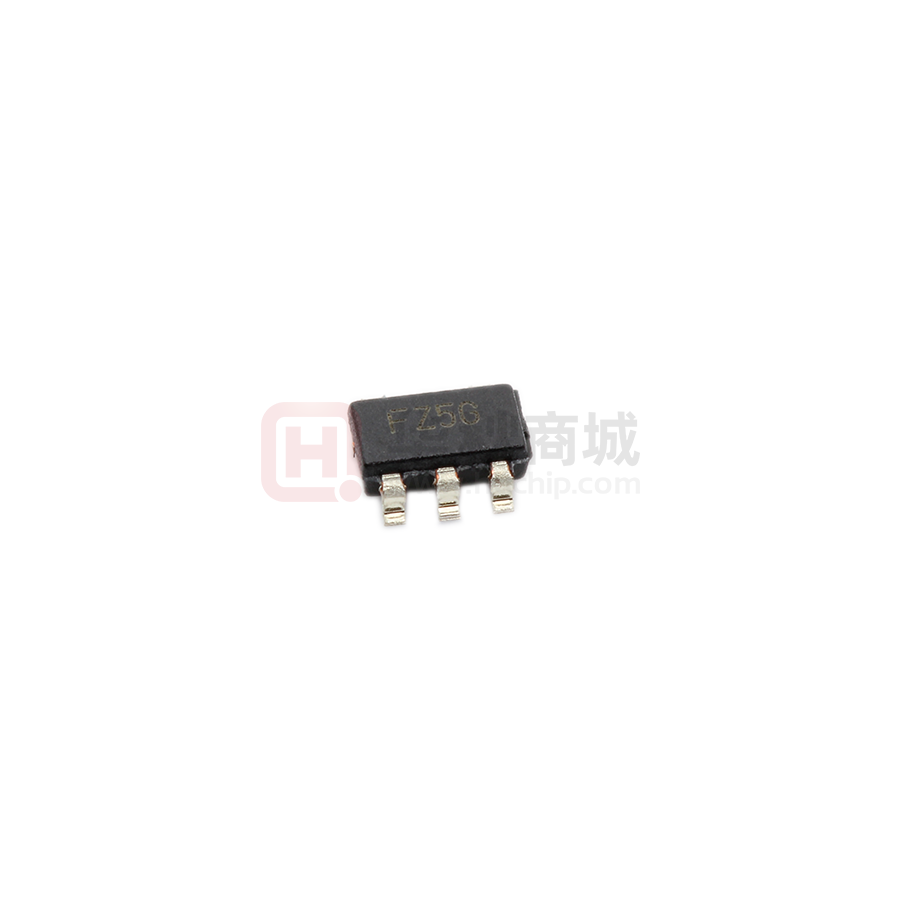
Package Types
SOT-23-5
MCP1415
MCP1416
5 OUT
NC 1
VDD 2
4 GND
IN 3
NC
1
VDD
2
IN
3
MCP1415R
NC 1
2008-2016 Microchip Technology Inc.
4 GND
MCP1416R
5 VDD
GND 2
IN 3
5 OUT
NC 1
5 VDD
GND 2
4 OUT
IN 3
4 OUT
DS20002092G-page 1
�MCP1415/16
Functional Block Diagram
Inverting
VDD
650 μA
300 mV
Output
Non-inverting
Input
Effective
Input C = 25 pF
(Each Input)
4.7V
MCP1415 Inverting
MCP1416 Non-inverting
GND
Note:
DS20002092G-page 2
Unused inputs should be grounded.
2008-2016 Microchip Technology Inc.
�MCP1415/16
1.0
† Notice: Stresses above those listed under “Maximum
Ratings” may cause permanent damage to the device.
This is a stress rating only and functional operation of
the device at those or any other conditions above those
indicated in the operational sections of this
specification is not intended. Exposure to maximum
rating conditions for extended periods may affect
device reliability.
ELECTRICAL
CHARACTERISTICS
Absolute Maximum Ratings †
VDD, Supply Voltage.............................................+20V
VIN, Input Voltage..............(VDD + 0.3V) to (GND - 5V)
Package Power Dissipation (TA = 50°C)
5L SOT23......................................................0.39W
ESD Protection on all Pins ......................2.0 kV (HBM)
................................................................... 300V (MM)
DC CHARACTERISTICS
Electrical Specifications: Unless otherwise noted, TA = +25°C, with 4.5V VDD 18V
Parameters
Conditions
Sym.
Min.
Typ.
Max.
Units
Logic ‘1’ High Input Voltage
VIH
2.4
1.9
—
V
Logic ‘0’ Low Input Voltage
VIL
—
1.6
0.8
V
Input Current
IIN
-1
—
+1
μA
Input Voltage
VIN
-5
—
VDD + 0.3
V
High Output Voltage
VOH
VDD - 0.025
—
—
V
DC Test
Low Output Voltage
VOL
—
—
0.025
V
DC Test
Output Resistance, High
ROH
—
6
7.5
IOUT = 10 mA, VDD = 18V
(Note 1)
Output Resistance, Low
ROL
—
4
5.5
IOUT = 10 mA, VDD = 18V
(Note 1)
Peak Output Current
IPK
—
1.5
—
A
VDD = 18V (Note 1)
Latch-Up Protection Withstand
Reverse Current
IREV
0.5
—
—
A
Duty cycle 2%, t 300 μs
(Note 1)
Rise Time
tR
—
18
25
ns
VDD = 18V, CL = 1000 pF
Figure 4-1, Figure 4-2 (Note 1)
Fall Time
tF
—
21
28
ns
VDD = 18V, CL = 1000 pF
Figure 4-1, Figure 4-2 (Note 1)
Delay Time
tD1
—
44
54
ns
VDD = 18V, VIN = 5V
Figure 4-1, Figure 4-2 (Note 1)
MCP1415 Delay Time
tD2
—
47
57
ns
VDD = 18V, VIN = 5V
Figure 4-1 (Note 1)
MCP1416 Delay Time
tD2
—
54
64
ns
VDD = 18V, VIN = 5V
Figure 4-2 (Note 1)
VDD
4.5
—
18
V
IS
—
0.65
1.1
mA
VIN = 3V
IS
—
0.1
0.15
mA
VIN = 0V
Input
0V VIN VDD
Output
Switching Time (Note 1)
Power Supply
Supply Voltage
Power Supply Current
Note 1:
Tested during characterization, not production tested.
2008-2016 Microchip Technology Inc.
DS20002092G-page 3
�MCP1415/16
DC CHARACTERISTICS (OVER OPERATING TEMPERATURE RANGE) (Note 1)
Electrical Specifications: Unless otherwise indicated, over the operating range with 4.5V VDD 18V.
Parameters
Typ.
Max.
Conditions
Sym.
Min.
Units
Logic ‘1’, High Input Voltage
VIH
2.4
—
—
V
Logic ‘0’, Low Input Voltage
VIL
—
—
0.8
V
Input Current
IIN
-10
—
+10
μA
Input Voltage
VIN
-5
—
VDD + 0.3
V
VOH
VDD - 0.025
—
—
V
DC Test
Input
0V VIN VDD
Output
High Output Voltage
Low Output Voltage
VOL
—
—
0.025
V
DC Test
Output Resistance, High
ROH
—
8.5
9.5
IOUT = 10 mA, VDD = 18V
Output Resistance, Low
ROL
—
6
7
IOUT = 10 mA, VDD = 18V
Rise Time
tR
—
26
37
ns
VDD = 18V, CL = 1000 pF
Figure 4-1, Figure 4-2
Fall Time
tF
—
29
40
ns
VDD = 18V, CL = 1000 pF
Figure 4-1, Figure 4-2
Delay Time
tD1
—
60
70
ns
VDD = 18V, VIN = 5V
Figure 4-1, Figure 4-2
MCP1415 Delay Time
tD2
—
62
72
ns
VDD = 18V, VIN = 5V
Figure 4-1
MCP1416 Delay Time
tD2
—
72
82
ns
VDD = 18V, VIN = 5V
Figure 4-2
VDD
4.5
—
18
V
IS
—
0.75
1.5
mA
VIN = 3.0V
IS
—
0.15
0.25
mA
VIN = 0V
Switching Time
Power Supply
Supply Voltage
Power Supply Current
Note 1:
Tested during characterization, not production tested.
TEMPERATURE CHARACTERISTICS
Electrical Specifications: Unless otherwise noted, all parameters apply with 4.5V VDD 18V
Parameter
Sym.
Min.
Typ.
Max.
Units
Comments
Temperature Ranges
Specified Temperature Range
TA
-40
—
+125
°C
Maximum Junction Temperature
TJ
—
—
+150
°C
Storage Temperature Range
TA
-65
—
+150
°C
JA
—
220.7
—
°C/W
Package Thermal Resistances
Thermal Resistance, 5LD SOT23
DS20002092G-page 4
2008-2016 Microchip Technology Inc.
�MCP1415/16
2.0
TYPICAL PERFORMANCE CURVES
Note:
The graphs and tables provided following this note are a statistical summary based on a limited number of
samples and are provided for informational purposes only. The performance characteristics listed herein are
not tested or guaranteed. In some graphs or tables, the data presented may be outside the specified
operating range (e.g., outside specified power supply range) and therefore outside the warranted range.
Note: Unless otherwise indicated, TA = +25°C with 4.5V VDD = 18V.
FIGURE 2-4:
Voltage.
Fall Time vs. Supply
FIGURE 2-2:
Load.
Rise Time vs. Capacitive
FIGURE 2-5:
Load.
Fall Time vs. Capacitive
32
30
28
26
24
22
20
18
16
14
12
Propagation Delay (ns)
Rise Time vs. Supply
Time (ns)
FIGURE 2-1:
Voltage.
tFALL
tRISE
-40 -25 -10
5
20
35
50
65
80
95 110 125
Temperature (°C)
FIGURE 2-3:
Temperature.
Rise and Fall Times vs.
2008-2016 Microchip Technology Inc.
120
110
100
90
80
70
60
50
40
30
20
VDD = 18V
tD1
MCP1416 tD2
MCP1415 tD2
2
4
6
8
10
12
Input Amplitude (V)
FIGURE 2-6:
Input Amplitude.
Propagation Delay Time vs.
DS20002092G-page 5
�MCP1415/16
Propagation Delay (ns)
Note: Unless otherwise indicated, TA = +25°C with 4.5V VDD = 18V.
140
130
120
110
100
90
80
70
60
50
40
30
20
VIN = 5V
MCP1416 tD2
MCP1415 tD2
tD1
4
6
8
10
12
14
16
18
Supply Voltage(V)
FIGURE 2-7:
Supply Voltage.
80
Propagation Delay (ns)
70
Propagation Delay Time vs.
VIN = 5V
VDD = 18V
FIGURE 2-10:
Temperature.
Quiescent Current vs.
MCP1416 tD2
60
MCP1415 tD2
50
tD1
40
30
20
-40 -25 -10
5
20
35
50
65
80
95 110 125
Temperature (°C)
FIGURE 2-8:
Temperature.
Propagation Delay Time vs.
FIGURE 2-11:
Voltage.
Input Threshold vs. Supply
FIGURE 2-9:
Supply Voltage.
Quiescent Current vs.
FIGURE 2-12:
Temperature.
Input Threshold vs.
DS20002092G-page 6
2008-2016 Microchip Technology Inc.
�MCP1415/16
Note: Unless otherwise indicated, TA = +25°C with 4.5V VDD = 18V.
FIGURE 2-13:
Capacitive Load.
Supply Current vs.
FIGURE 2-16:
Frequency.
Supply Current vs.
FIGURE 2-14:
Capacitive Load.
Supply Current vs.
FIGURE 2-17:
Frequency.
Supply Current vs.
FIGURE 2-15:
Capacitive Load.
Supply Current vs.
FIGURE 2-18:
Frequency.
Supply Current vs.
2008-2016 Microchip Technology Inc.
DS20002092G-page 7
�MCP1415/16
Note: Unless otherwise indicated, TA = +25°C with 4.5V VDD = 18V.
FIGURE 2-19:
Output Resistance (Output
High) vs. Supply Voltage.
FIGURE 2-20:
Output Resistance (Output
Low) vs. Supply Voltage.
FIGURE 2-21:
Supply Voltage.
DS20002092G-page 8
Crossover Energy vs.
2008-2016 Microchip Technology Inc.
�MCP1415/16
3.0
PIN DESCRIPTIONS
The descriptions of the pins are listed in Table 3-1.
TABLE 3-1:
PIN FUNCTION TABLE
Pin No.
Symbol
Description
MCP1415/16
MCP1415R/16R
1
1
NC
No Connection
3.1
2
5
VDD
Supply Input
3
3
IN
Control Input
4
2
GND
Ground
5
4
OUT/OUT
Output
Supply Input (VDD)
3.3
Ground (GND)
VDD is the bias supply input for the MOSFET driver and
has a voltage range of 4.5V to 18V. This input must be
decoupled to ground with a local capacitor. This bypass
capacitor provides a localized low-impedance path for
the peak currents that are provided to the load.
Ground is the device return pin. The ground pin should
have a low-impedance connection to the bias supply
source return. When the capacitive load is being
discharged, high peak currents will flow out of the
ground pin.
3.2
3.4
Control Input (IN)
The MOSFET driver input is a high-impedance,
TTL/CMOS compatible input. The input also has
hysteresis between the high and low input levels,
allowing them to be driven from slow rising and falling
signals and to provide noise immunity.
2008-2016 Microchip Technology Inc.
Output (OUT, OUT)
The output is a CMOS push-pull output that is capable
of sourcing and sinking 1.5A of peak current
(VDD = 18V). The low output impedance ensures the
gate of the external MOSFET stays in the intended
state even during large transients. This output also has
a reverse current latch-up rating of 500 mA.
DS20002092G-page 9
�MCP1415/16
4.0
APPLICATION INFORMATION
4.1
General Information
VDD = 18V
MOSFET drivers are high-speed, high-current devices
which are intended to source/sink high peak currents to
charge/discharge the gate capacitance of external
MOSFETs or Insulated-Gate Bipolar Transistors
(IGBTs). In high frequency switching power supplies,
the Pulse-Width Modulation (PWM) controller may not
have the drive capability to directly drive the power
MOSFET. A MOSFET driver such as the MCP1415/16
family can be used to provide additional source/sink
current capability.
4.2
MOSFET Driver Timing
1 μF
Input
Output
C L = 1000 pF
MCP1416
+5V
The ability of a MOSFET driver to transition from a
fully-off state to a fully-on state is characterized by the
driver’s rise time (tR), fall time (tF) and propagation
delays (tD1 and tD2). Figure 4-1 and Figure 4-2 show
the test circuit and timing waveform used to verify the
MCP1415/16 timing.
0.1 μF
Ceramic
90%
Input
0V
10%
18V
tD1 90%
Output
tR
tD2
10%
0V
90%
tF
10%
VDD = 18V
1 μF
0.1 μF
Ceramic
Note:
Input Signal: tRISE = tFALL ≤ 10 ns
100 Hz, 0-5V Square Wave
FIGURE 4-2:
Waveform.
Input
Output
C L = 1000 pF
4.3
MCP1415
+5V
90%
10%
18V
tF
tD2
tR
90%
90%
Output
10%
0V
Note:
tD1
Decoupling Capacitors
Careful layout and decoupling capacitors are required
when using power MOSFET drivers. Large current is
required to charge and discharge capacitive loads
quickly. For example, approximately 720 mA are
needed to charge a 1000 pF load with 18V in 25 ns.
Input
0V
Non-Inverting Driver Timing
10%
To operate the MOSFET driver over a wide frequency
range with low supply impedance, it is recommended to
place a ceramic and a low ESR film capacitor in parallel
between the driver VDD and GND. A 1.0 μF low ESR
film capacitor and a 0.1 μF ceramic capacitor placed
between pins 2 and 4 are required for reliable
operation. These capacitors should be placed close to
the driver to minimize circuit board parasitics and
provide a local source for the required current.
Input Signal: tRISE = tFALL ≤ 10 ns
100 Hz, 0-5V Square Wave
FIGURE 4-1:
Waveform.
DS20002092G-page 10
Inverting Driver Timing
2008-2016 Microchip Technology Inc.
�MCP1415/16
4.4
4.4.3
Power Dissipation
The total internal power dissipation in a MOSFET driver
is the summation of three separate power dissipation
elements.
EQUATION 4-1:
P T = P L + P Q + P CC
OPERATING POWER DISSIPATION
The operating power dissipation occurs each time the
MOSFET driver output transitions because, for a very
short period of time, both MOSFETs in the output stage
are on simultaneously. This cross-conduction current
leads to a power dissipation described in Equation 4-4.
EQUATION 4-4:
Where:
P CC = CC f V DD
PT
=
Total power dissipation
PL
=
Load power dissipation
PQ
=
Quiescent power dissipation
PCC
=
Operating power dissipation
4.4.1
Where:
CC
=
Cross-Conduction constant
(A*sec)
f
=
Switching frequency
VDD
=
MOSFET driver supply voltage
CAPACITIVE LOAD DISSIPATION
The power dissipation caused by a capacitive load is a
direct function of the frequency, total capacitive load
and supply voltage. The power lost in the MOSFET
driver for a complete charging and discharging cycle of
a MOSFET is shown in Equation 4-2.
EQUATION 4-2:
P L = f C T V DD
Where:
2
f
=
Switching frequency
CT
=
Total load capacitance
VDD
=
MOSFET driver supply voltage
4.4.2
4.5
PCB Layout Considerations
Proper PCB layout is important in high-current, fast
switching circuits to provide proper device operation
and robustness of design. Improper component
placement may cause errant switching, excessive
voltage ringing or circuit latch-up. PCB trace loop area
and inductance must be minimized. This is
accomplished by placing the MOSFET driver directly at
the load and placing the bypass capacitor directly at the
MOSFET driver (see Figure 4-3). Locating ground
planes or ground return traces directly beneath the
driver output signal reduces trace inductance. A ground
plane also helps as a radiated noise shield and it provides some heat sinking for power dissipated within the
device (see Figure 4-4).
QUIESCENT POWER DISSIPATION
The power dissipation associated with the quiescent
current draw depends on the state of the input pin. The
MCP1415/16 devices have a quiescent current draw of
0.65 mA (typical) when the input is high and of 0.1 mA
(typical) when the input is low. The quiescent power
dissipation is shown in Equation 4-3.
EQUATION 4-3:
P Q = I QH D + I QL 1 – D V DD
Where:
IQH
=
Quiescent current in the High
state
D
=
Duty cycle
IQL
=
Quiescent current in the Low
state
VDD
=
MOSFET driver supply voltage
2008-2016 Microchip Technology Inc.
FIGURE 4-3:
(TOP).
Recommended PCB Layout
FIGURE 4-4:
(BOTTOM).
Recommended PCB Layout
DS20002092G-page 11
�MCP1415/16
5.0
PACKAGING INFORMATION
5.1
Package Marking Information
Example
5-Lead SOT-23
Standard Markings for SOT-23
Part Number
XXNN
Legend: XX...X
Y
YY
WW
NNN
e3
*
Note:
MCP1415T-E/OT
Code
FYNN
MCP1415RT-E/OT
F7NN
MCP1416T-E/OT
FZNN
MCP1416RT-E/OT
F8NN
FYNN
Customer-specific information
Year code (last digit of calendar year)
Year code (last 2 digits of calendar year)
Week code (week of January 1 is week ‘01’)
Alphanumeric traceability code
Pb-free JEDEC® designator for Matte Tin (Sn)
This package is Pb-free. The Pb-free JEDEC designator ( e3 )
can be found on the outer packaging for this package.
In the event the full Microchip part number cannot be marked on one line, it will be carried over
to the next line, thus limiting the number of available characters for customer-specific
information.
DS20002092G-page 12
2008-2016 Microchip Technology Inc.
�MCP1415/16
�������
���
�����
����
��������
������������������
�����
)RU�WKH�PRVW�FXUUHQW�SDFNDJH�GUDZLQJV��SOHDVH�VHH�WKH�0LFURFKLS�3DFNDJLQJ�6SHFLILFDWLRQ�ORFDWHG�DW�
KWWS���ZZZ�PLFURFKLS�FRP�SDFNDJLQJ
b
N
E
E1
3
2
1
e
e1
D
A2
A
c
φ
A1
L
L1
8QLWV
'LPHQVLRQ�/LPLWV
1XPEHU�RI�3LQV
0,//,0(7(56
0,1
120
0$;
1
�
/HDG�3LWFK
H
�����%6&
2XWVLGH�/HDG�3LWFK
H�
2YHUDOO�+HLJKW
$
����
±
0ROGHG�3DFNDJH�7KLFNQHVV
$�
����
±
����
6WDQGRII
$�
����
±
����
2YHUDOO�:LGWK
(
����
±
����
0ROGHG�3DFNDJH�:LGWK
(�
����
±
����
2YHUDOO�/HQJWK
'
����
±
����
�����%6&
����
)RRW�/HQJWK
/
����
±
����
)RRWSULQW
/�
����
±
����
)RRW�$QJOH
�
�
±
��
/HDG�7KLFNQHVV
F
����
±
����
/HDG�:LGWK
E
����
±
����
������
�� 'LPHQVLRQV�'�DQG�(��GR�QRW�LQFOXGH�PROG�IODVK�RU�SURWUXVLRQV��0ROG�IODVK�RU�SURWUXVLRQV�VKDOO�QRW�H[FHHG�������PP�SHU�VLGH�
�� 'LPHQVLRQLQJ�DQG�WROHUDQFLQJ�SHU�$60(�


 工商网监
湘ICP备2023018690号
工商网监
湘ICP备2023018690号