MCP14A0151/2
1.5A MOSFET Driver
with Low Threshold Input And Enable
Features
General Description
• High Peak Output Current: 1.5A (typical)
• Wide Input Supply Voltage Operating Range:
- 4.5V to 18V
• Low Shoot-Through/Cross-Conduction Current in
Output Stage
• High Capacitive Load Drive Capability:
- 1000 pF in 11.5 ns (typical)
• Short Delay Times: 33 ns (tD1), 24 ns (tD2) (typical)
• Low Supply Current: 375 µA (typical)
• Low-Voltage Threshold Input and Enable with
Hysteresis
• Latch-Up Protected: Withstands 500 mA Reverse
Current
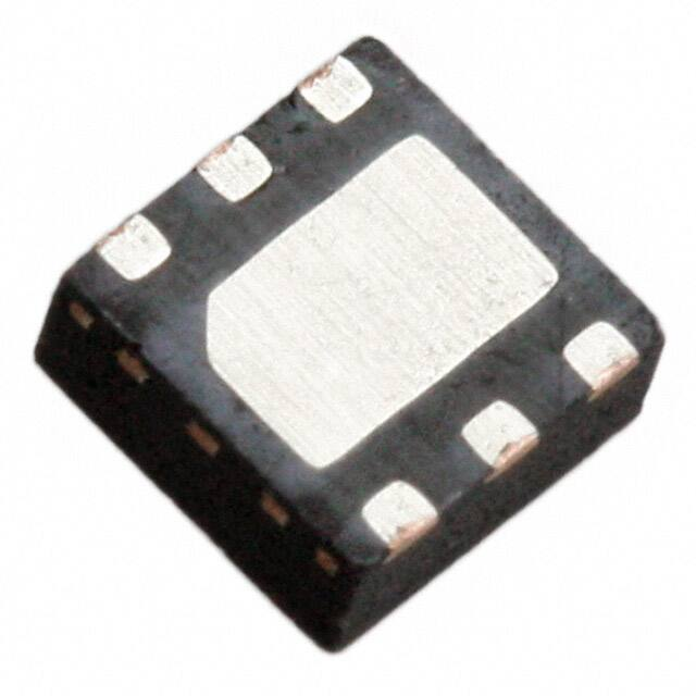
• Space-Saving Packages:
- 6L SOT-23
- 6L 2 x 2 DFN
The MCP14A0151/2 devices are high-speed MOSFET
drivers that are capable of providing up to 1.5A of peak
current while operating from a single 4.5V to 18V
supply. The inverting (MCP14A0151) or non-inverting
(MCP14A0152) single channel output is directly
controlled from either TTL or CMOS (2V to 18V) logic.
These devices also feature low shoot-through current,
matched rise and fall times, and short propagation
delays which make them ideal for high switching
frequency applications.
Applications
•
•
•
•
•
Switch Mode Power Supplies
Pulse Transformer Drive
Line Drivers
Level Translator
Motor and Solenoid Drive
The MCP14A0151/2 family of devices offer enhanced
control with Enable functionality. The active-high
Enable pin can be driven low to drive the output of the
MCP14A0151/2 low, regardless of the status of the
Input pin. An integrated pull-up resistor allows the user
to leave the Enable pin floating for standard operation.
Additionally, the MCP14A0151/2 devices feature separate ground pins (AGND and GND), allowing greater
noise isolation between the level-sensitive Input/
Enable pins and the fast, high-current transitions of the
push-pull output stage.
These devices are highly latch-up resistant under any
condition within their power and voltage ratings. They
can accept up to 500 mA of reverse current being
forced back into their outputs without damage or logic
upset. All terminals are fully protected against
electrostatic discharge (ESD) up to 1.75 kV (HBM) and
200V (MM).
Package Types
6-Lead SOT-23
MCP14A0151
MCP14A0152
VDD
1
6
OUT
AGND
2
5
GND
IN
3
4
EN
OUT
MCP14A0152
OUT
MCP14A0151
OUT 1
GND 2
EN 3
2x2 DFN-6*
6 VDD
EP
7
5 IN
4 AGND
* Includes Exposed Thermal Pad (EP); see Table 3-1.
2014 Microchip Technology Inc.
DS20005368A-page 1
�MCP14A0151/2
Functional Block Diagram
DS20005368A-page 2
2014 Microchip Technology Inc.
�MCP14A0151/2
1.0
† Notice: Stresses above those listed under “Maximum
Ratings” may cause permanent damage to the device.
This is a stress rating only and functional operation of
the device at those or any other conditions above those
indicated in the operational sections of this
specification is not intended. Exposure to maximum
rating conditions for extended periods may affect
device reliability.
ELECTRICAL
CHARACTERISTICS
Absolute Maximum Ratings †
VDD, Supply Voltage............................................. +20V
VIN, Input Voltage........... (VDD + 0.3V) to (GND - 0.3V)
VEN, Enable Voltage....... (VDD + 0.3V) to (GND - 0.3V)
Package Power Dissipation (TA = +50°C)
6L SOT-23.................................................... 0.52 W
6L 2 x 2 DFN ................................................ 1.09 W
ESD Protection on all Pins ....................1.75 kV (HBM)
....................................................................200V (MM)
DC CHARACTERISTICS
Electrical Specifications: Unless otherwise noted, TA = +25°C, with 4.5V VDD 18V.
Parameters
Sym.
Min.
Typ.
Max.
Units
Conditions
Input Voltage Range
VIN
GND - 0.3V
—
VDD + 0.3
V
Logic ‘1’ High Input Voltage
VIH
2.0
1.6
—
V
Logic ‘0’ Low Input Voltage
VIL
—
1.2
0.8
V
VHYST(IN)
—
0.4
—
V
IIN
-1
—
+1
µA
Enable Voltage Range
VEN
GND - 0.3V
—
VDD + 0.3
V
Logic ‘1’ High Enable Voltage
VEH
2.0
1.6
—
V
Logic ‘0’ Low Enable Voltage
VEL
—
1.2
0.8
V
VHYST(EN)
—
0.4
—
V
RENBL
—
1.8
—
MΩ
VDD = 18V, ENB = AGND
Enable Input Current
IEN
—
10
—
µA
VDD = 18V, ENB = AGND
Propagation Delay
tD3
—
34
41
ns
VDD = 18V, VEN = 5V, see
Figure 4-3, (Note 1)
Propagation Delay
tD4
—
23
30
ns
VDD = 18V, VEN = 5V, see
Figure 4-3, (Note 1)
VOH
VDD - 0.025
—
—
V
IOUT = 0A
Low Output Voltage
VOL
—
—
0.025
V
IOUT = 0A
Output Resistance, High
ROH
—
4.5
6.5
Ω
IOUT = 10 mA, VDD = 18V
Output Resistance, Low
ROL
—
3
4.5
Ω
IOUT = 10 mA, VDD = 18V
Peak Output Current
IPK
—
1.5
—
A
VDD = 18V (Note 1)
Latch-Up Protection Withstand
Reverse Current
IREV
0.5
—
—
A
Duty cycle 2%, t 300 µs
(Note 1)
Rise Time
tR
—
11.5
18.5
ns
VDD = 18V, CL = 1000 pF, see
Figure 4-1, Figure 4-2
(Note 1)
Fall Time
tF
—
10
17
ns
VDD = 18V, CL = 1000 pF, see
Figure 4-1, Figure 4-2
(Note 1)
Note 1:
Tested during characterization, not production tested.
Input
Input Voltage Hysteresis
Input Current
0V VIN VDD
Enable
Enable Voltage Hysteresis
Enable Pin Pull-Up Resistance
Output
High Output Voltage
Switching Time (Note 1)
2014 Microchip Technology Inc.
DS20005368A-page 3
�MCP14A0151/2
DC CHARACTERISTICS (CONTINUED)
Electrical Specifications: Unless otherwise noted, TA = +25°C, with 4.5V VDD 18V.
Parameters
Delay Time
Sym.
Min.
Typ.
Max.
Units
Conditions
tD1
—
33
40
ns
VDD = 18V, VIN = 5V, see
Figure 4-1, Figure 4-2
(Note 1)
tD2
—
24
31
ns
VDD = 18V, VIN = 5V, see
Figure 4-1, Figure 4-2
(Note 1)
VDD
4.5
—
18
V
IDD
—
330
560
µA
VIN = 3V, VEN = 3V
IDD
—
360
580
µA
VIN = 0V, VEN = 3V
IDD
—
360
580
µA
VIN = 3V, VEN = 0V
IDD
—
375
600
µA
VIN = 0V, VEN = 0V
Power Supply
Supply Voltage
Power Supply Current
Note 1:
Tested during characterization, not production tested.
DC CHARACTERISTICS (OVER OPERATING TEMP. RANGE) (Note 1)
Electrical Specifications: Unless otherwise indicated, over the operating range with 4.5V VDD 18V.
Parameters
Sym.
Min.
Typ.
Max.
Input Voltage Range
VIN
Logic ‘1’ High Input Voltage
VIH
Logic ‘0’ Low Input Voltage
Units
GND - 0.3V
—
VDD + 0.3
V
2.0
1.6
—
V
VIL
—
1.2
0.8
V
VHYST(IN)
—
0.4
—
V
IIN
-10
—
+10
µA
Enable Voltage Range
VEN
GND - 0.3V
—
VDD + 0.3
V
Logic ‘1’ High Enable Voltage
VEH
2.0
1.6
—
V
Logic ‘0’ Low Enable Voltage
VEL
—
1.2
0.8
V
VHYST(EN)
—
0.4
—
V
Conditions
Input
Input Voltage Hysteresis
Input Current
0V VIN VDD
Enable
Enable Voltage Hysteresis
Enable Input Current
IEN
—
12
—
µA
VDD = 18V, ENB = AGND
Propagation Delay
tD3
—
32
39
ns
VDD = 18V, VEN = 5V, TA = +125°C,
see Figure 4-3
Propagation Delay
tD4
—
25
32
ns
VDD = 18V, VEN = 5V, TA = +125°C,
see Figure 4-3
VOH
VDD - 0.025
—
—
V
DC Test
Low Output Voltage
VOL
—
—
0.025
V
DC Test
Output Resistance, High
ROH
—
—
9
Ω
IOUT = 10 mA, VDD = 18V
Output Resistance, Low
ROL
—
—
6.5
Ω
IOUT = 10 mA, VDD = 18V
Output
High Output Voltage
Note 1:
Tested during characterization, not production tested.
DS20005368A-page 4
2014 Microchip Technology Inc.
�MCP14A0151/2
DC CHARACTERISTICS (OVER OPERATING TEMP. RANGE) (Note 1) (CONTINUED)
Electrical Specifications: Unless otherwise indicated, over the operating range with 4.5V VDD 18V.
Parameters
Sym.
Min.
Typ.
Max.
Units
Conditions
Rise Time
tR
—
14
21
ns
VDD = 18V, CL = 1000 pF,
TA = +125°C, see Figure 4-1,
Figure 4-2
Fall Time
tF
—
13
20
ns
VDD = 18V, CL = 1000 pF,
TA = +125°C, see Figure 4-1,
Figure 4-2
Delay Time
tD1
—
31
38
ns
VDD = 18V, VIN = 5V, TA = +125°C,
see Figure 4-1, Figure 4-2
tD2
—
26
33
VDD
4.5
—
18
V
Switching Time (Note 1)
VDD = 18V, VIN = 5V, TA = +125°C,
see Figure 4-1, Figure 4-2
Power Supply
Supply Voltage
Power Supply Current
Note 1:
IDD
—
—
760
uA
VIN = 3V, VEN = 3V
IDD
—
—
780
uA
VIN = 0V, VEN = 3V
IDD
—
—
780
uA
VIN = 3V, VEN = 0V
IDD
—
—
800
uA
VIN = 0V, VEN = 0V
Tested during characterization, not production tested.
TEMPERATURE CHARACTERISTICS
Electrical Specifications: Unless otherwise noted, all parameters apply with 4.5V VDD 18V
Parameter
Sym.
Min.
Typ.
Max.
Units
TA
-40
—
+125
°C
Comments
Temperature Ranges
Specified Temperature Range
Maximum Junction Temperature
TJ
—
—
+150
°C
Storage Temperature Range
TA
-65
—
+150
°C
Thermal Resistance, 6LD 2x2 DFN
JA
—
91
—
°C/W
Thermal Resistance, 6LD SOT-23
JA
—
192
—
°C/W
Package Thermal Resistances
2014 Microchip Technology Inc.
DS20005368A-page 5
�MCP14A0151/2
2.0
TYPICAL PERFORMANCE CURVES
The graphs and tables provided following this note are a statistical summary based on a limited number of
samples and are provided for informational purposes only. The performance characteristics listed herein
are not tested or guaranteed. In some graphs or tables, the data presented may be outside the specified
operating range (e.g., outside specified power supply range) and therefore outside the warranted range.
Note:
Note: Unless otherwise indicated, TA = +25°C with 4.5V VDD 18V.
160
200
140
180
120
140
10000 pF
120
100
6800 pF
80
60
3300 pF
470 pF
40
20
Fall Time (ns)
Rise Time (ns)
160
5V
100
12V
80
60
40
1000 pF
20
18V
0
4
6
8
10
12
14
16
0
18
100
Supply Voltage (V)
FIGURE 2-1:
Voltage.
FIGURE 2-4:
Load.
Rise Time vs. Supply
200
Fall Time vs. Capacitive
VDD = 18V
Time (ns)
140
120
12V
100
18V
80
tR, 1000 pF
14
5V
160
Rise Time (ns)
10000
16
180
12
tF, 1000 pF
10
tR, 470 pF
8
60
tF, 470 pF
6
40
20
4
0
-40 -25 -10
100
1000
Capacitive Load (pF)
FIGURE 2-2:
Load.
10000
Rise Time vs. Capacitive
5
20 35 50 65 80 95 110 125
Temperature (°C)
FIGURE 2-5:
Temperature.
160
Rise and Fall Time vs.
10000
Crossover Current (µA)
140
120
Fall Time (ns)
1000
Capacitive Load (pF)
100
10000 pF
80
60
6800 pF
40
3300 pF
470 pF
20
500k Hz
200 kHz
100 kHz
50 kHz
1000
100
10
1000 pF
1
0
4
6
8
10
12
14
16
18
4
6
FIGURE 2-3:
Voltage.
DS20005368A-page 6
Fall Time vs. Supply
8
10
12
14
16
18
Supply Voltage (V)
Supply Voltage (V)
FIGURE 2-6:
Supply Voltage.
Crossover Current vs.
2014 Microchip Technology Inc.
�MCP14A0151/2
Note: Unless otherwise indicated, TA = +25°C with 4.5V VDD 18V.
45
VIN = 5V
Enable Propagation Delay (ns)
Input Propagation Delay (ns)
45
40
35
tD1
30
tD2
25
20
VEN = 5V
40
35
tD3
30
tD4
25
20
4
6
8
10
12
14
16
18
4
6
8
Supply Voltage (V)
FIGURE 2-7:
Supply Voltage.
Input Propagation Delay vs.
14
16
18
40
VDD = 18V
35
Enable Propagation Delay (ns)
Input Propogation Delay (ns)
12
FIGURE 2-10:
Enable Propagation Delay
vs. Supply Voltage.
40
tD1
30
tD2
25
20
15
VDD = 18V
tD3
35
30
25
tD4
20
15
4
6
8
10
12
14
16
18
4
Input Voltage Amplitude (V)
VDD = 18V
VIN = 5V
35
tD1
30
tD2
25
8
10
12
14
16
18
FIGURE 2-11:
Enable Propagation Delay
Time vs. Enable Voltage Amplitude.
45
Enable Propagation Delay (ns)
40
6
Enable Voltage Amplitude (V)
FIGURE 2-8:
Input Propagation Delay
Time vs. Input Amplitude.
Input Propagation Delay (ns)
10
Supply Voltage (V)
VDD = 18V
VEN = 5V
40
tD3
35
30
25
tD4
20
20
-40 -25 -10
5
20 35 50 65 80 95 110 125
-40 -25 -10
FIGURE 2-9:
Temperature.
Input Propagation Delay vs.
2014 Microchip Technology Inc.
5
20 35 50 65 80 95 110 125
Temperature (°C)
Temperature (°C)
FIGURE 2-12:
vs. Temperature.
Enable Propagation Delay
DS20005368A-page 7
�MCP14A0151/2
Note: Unless otherwise indicated, TA = +25°C with 4.5V VDD 18V.
1.8
1.7
VIN = 0V,VEN = 0V
Input Threshold (V)
Quiescent Current (µA)
400
350
VIN = 3V,VEN = 3V
300
VIN = 3V,VEN = 0V or VIN = 0V,VEN = 3V
VIH
1.6
1.5
1.4
1.3
VIL
1.2
1.1
250
1
4
6
8
10
12
14
16
18
4
6
Supply Voltage (V)
FIGURE 2-16:
Voltage.
550
450
VIN = 0V,VEN = 0V
VIN = 5V,VEN = 5V
350
300
250
VIN = 5V,VEN = 0V or VIN = 0V,VEN = 5V
18
Input Threshold vs Supply
VDD = 18V
VEH
1.6
1.5
1.4
1.3
VEL
1.2
1.1
1
0.8
-40 -25 -10
5
20 35 50 65 80 95 110 125
-40 -25 -10
5
Temperature (°C)
FIGURE 2-14:
vs. Temperature.
FIGURE 2-17:
Temperature.
1.7
Enable Threshold (V)
VIH
1.5
1.4
VIL
1.1
1
Enable Threshold vs.
1.8
VDD = 18V
1.7
20 35 50 65 80 95 110 125
Temperature (°C)
Quiescent Supply Current
1.8
Input Threshold (V)
16
0.9
200
1.2
14
1.7
Enable Threshold (V)
Quiescent Current (µA)
500
1.3
12
1.8
VDD = 18V
1.6
10
Supply Voltage (V)
FIGURE 2-13:
Quiescent Supply Current
vs. Supply Voltage.
400
8
VEH
1.6
1.5
1.4
1.3
VEL
1.2
1.1
0.9
0.8
1
-40 -25 -10
5
20 35 50 65 80 95 110 125
4
6
Temperature (°C)
FIGURE 2-15:
Temperature.
DS20005368A-page 8
Input Threshold vs.
8
10
12
14
16
18
Supply Voltage (V)
FIGURE 2-18:
Voltage.
Enable Threshold vs Supply
2014 Microchip Technology Inc.
�MCP14A0151/2
Note: Unless otherwise indicated, TA = +25°C with 4.5V VDD 18V.
14
ROH - Output Resistance (Ω)
50
VIN = 0V (MCP14A0151)
VIN = 5V (MCP14A0152)
13
Supply Current (mA)
12
11
TA = +125°C
10
9
8
7
6
40
30
25
20
15
10
0
4
100
4
6
8
10
12
14
Supply Voltage (V)
16
1000
18
FIGURE 2-19:
Output Resistance (Output
High) vs. Supply Voltage.
10000
Capacitive Load (pF)
FIGURE 2-22:
Supply Current vs.
Capacitive Load (VDD = 12V).
10
30
VIN = 5V (MCP14A0151)
VIN = 0V (MCP14A0152)
VDD = 6V
8
Supply Current (mA)
ROL - Output Resistance (Ω)
1 MHz
500 kHz
200 kHz
100 kHz
50 kHz
10 kHz
35
5
TA = +25°C
5
VDD = 12V
45
TA = +125°C
6
4
TA = +25°C
2
25
1 MHz
500 kHz
200 kHz
100 kHz
50 kHz
10 kHz
20
15
10
5
0
0
100
4
6
8
10
12
14
Supply Voltage (V)
16
FIGURE 2-20:
Output Resistance (Output
Low) vs. Supply Voltage.
100
FIGURE 2-23:
Supply Current vs.
Capacitive Load (VDD = 6V).
100
VDD = 18V
90
80
1 MHz
500 kHz
200 kHz
100 kHz
50 kHz
10 kHz
70
60
50
40
30
20
10
10000
Capacitive Load (pF)
Supply Current (mA)
Supply Current (mA)
90
1000
18
VDD = 18V
80
10000 pF
6800 pF
3300 pF
1000 pF
470 pF
100 pF
70
60
50
40
30
20
10
0
0
100
1000
Capacitive Load (pF)
FIGURE 2-21:
Supply Current vs.
Capacitive Load (VDD = 18V).
2014 Microchip Technology Inc.
10000
10
100
1000
Switching Frequency (kHz)
FIGURE 2-24:
Supply Current vs.
Frequency (VDD = 18V).
DS20005368A-page 9
�MCP14A0151/2
Note: Unless otherwise indicated, TA = +25°C with 4.5V VDD 18V.
50
VDD = 12V
Supply Current (mA)
45
40
10000 pF
6800 pF
3300 pF
1000 pF
470 pF
100 pF
35
30
25
20
15
10
5
0
10
100
1000
Switching Frequency (kHz)
FIGURE 2-25:
Supply Current vs.
Frequency (VDD = 12V).
30
Supply Current (mA)
VDD = 6V
25
10000 pF
6800 pF
3300 pF
1000 pF
470 pF
100 pF
20
15
10
5
0
10
100
1000
Switching Frequency (kHz)
FIGURE 2-26:
Supply Current vs.
Frequency (VDD = 6V).
14
Enable Current (uA)
13
TA = +125°C
12
11
TA = +25°C
10
9
8
4
6
8
10
12
14
Supply Voltage (V)
FIGURE 2-27:
Voltage.
DS20005368A-page 10
16
18
Enable Current vs. Supply
2014 Microchip Technology Inc.
�MCP14A0151/2
3.0
PIN DESCRIPTIONS
The descriptions of the pins are listed in Table 3-1.
TABLE 3-1:
PIN FUNCTION TABLE
Pin No.
Symbol
Description
6L 2x2 DFN
6L SOT-23
1
6
OUT/OUT
2
5
GND
Power Ground
3
4
EN
Device Enable
4
2
AGND
Analog Ground
5
3
IN
Control Input
3.1
Push-Pull Output
6
1
VDD
Supply Input
EP
—
EP
Exposed Thermal Pad (GND)
Output Pin (OUT, OUT)
The Output is a CMOS push-pull output that is capable
of sourcing and sinking 1.5A of peak current
(VDD = 18V). The low output impedance ensures the
gate of the external MOSFET stays in the intended
state even during large transients. This output also has
a reverse current latch-up rating of 500 mA.
3.5
The MOSFET driver Control Input is a high-impedance,
TTL/CMOS compatible input. The Input also has
hysteresis between the high and low input levels,
allowing them to be driven from slow rising and falling
signals and to provide noise immunity.
3.6
3.2
Power Ground Pin (GND)
GND is the device return pin for the output stage. The
GND pin should have a low-impedance connection to
the bias supply source return. When the capacitive load
is being discharged, high peak currents will flow out of
the ground pin.
Device Enable Pin (EN)
The MOSFET driver Device Enable is a highimpedance, TTL/CMOS compatible input. The Enable
input also has hysteresis between the high and low
input levels, allowing them to be driven from slow rising
and falling signals and to provide noise immunity.
Driving the Enable pin below the threshold will disable
the output of the device, pulling OUT/OUT low,
regardless of the status of the Input pin. Driving the
Enable pin above the threshold allows normal
operation of the OUT/OUT pin based on the status of
the Input pin. The Enable pin utilizes an internal pull up
resistor, allowing the pin to be left floating for standard
driver operation.
3.4
Supply Input Pin (VDD)
VDD is the bias supply input for the MOSFET driver and
has a voltage range of 4.5V to 18V. This input must be
decoupled to ground with a local capacitor. This bypass
capacitor provides a localized low-impedance path for
the peak currents that are provided to the load
3.7
3.3
Control Input Pin (IN)
Exposed Metal Pad Pin (EP)
The exposed metal pad of the DFN package is not
internally connected to any potential. Therefore, this
pad can be connected to a ground plane, or other copper plane on a printed circuit board, to aid in heat
removal from the package.
Analog Ground Pin (AGND)
AGND is the device return pin for the input and enable
stages of the MOSFET driver. The AGND pin should be
connected to an electrically “quiet” ground node to provide a low noise reference for the input and enable
pins.
2014 Microchip Technology Inc.
DS20005368A-page 11
�MCP14A0151/2
4.0
APPLICATION INFORMATION
VDD = 18V
4.1
General Information
MOSFET drivers are high-speed, high-current devices
which are intended to source/sink high-peak currents to
charge/discharge the gate capacitance of external
MOSFETs or Insulated-Gate Bipolar Transistors
(IGBTs). In high frequency switching power supplies,
the Pulse-Width Modulation (PWM) controller may not
have the drive capability to directly drive the power
MOSFET. A MOSFET driver such as the
MCP14A0151/2 family can be used to provide additional source/sink current capability.
4.2
Input
The ability of a MOSFET driver to transition from a fullyoff state to a fully-on state is characterized by the
driver’s rise time (tR), fall time (tF) and propagation
delays (tD1 and tD2). Figure 4-1 and Figure 4-2 show
the test circuit and timing waveform used to verify the
MCP14A0151/2 timing.
VDD = 18V
MCP14A0152
5V
VIH (Typ.)
0V
MCP14A0151
5V
Input
VIL (Typ.)
tF
tD2
tR
18V
90%
Output
0V
FIGURE 4-1:
Waveform.
DS20005368A-page 12
tD1
tR
tD2
tF
90%
Output
10%
0V
Non-Inverting Driver Timing
0.1 µF
Output
tD1
VIL (Typ.)
18V
FIGURE 4-2:
Waveform.
CL = 1000 pF
VIH (Typ.)
0V
Output
CL = 1000 pF
4.3
Input
0.1 µF
Input
MOSFET Driver Timing
1 µF
1 µF
10%
Inverting Driver Timing
Enable Function
The enable pin (EN) provides additional control of the
output pin (OUT). This pin is active high and is internally pulled up to VDD so that the pin can be left floating
to provide standard MOSFET driver operation.
When the enable pin’s voltage is above the enable pin
high voltage threshold, (VEN_H), the output is enabled
and allowed to react to the status of the Input pin.
However, when the voltage applied to the Enable pin
falls below the low threshold voltage (VEN_L), the driver
output is disabled and doesn't respond to changes in
the status of the Input pin. When the driver is disabled,
the output is pulled down to a low state. Refer to
Table 4-1 for enable pin logic. The threshold voltage
levels for the Enable pin are similar to the threshold
voltage levels of the Input pin, and are TTL and CMOS
compatible. Hysteresis is provided to help increase the
noise immunity of the enable function, avoiding false
triggers of the enable signal during driver switching.
There are propagation delays associated with the
driver receiving an enable signal and the output
reacting. These propagation delays, tD3 and tD4, are
graphically represented in Figure 4-3.
2014 Microchip Technology Inc.
�MCP14A0151/2
TABLE 4-1:
ENABLE PIN LOGIC
4.6
ENB
IN
MCP14A0151
OUT
MCP14A0152
OUT
H
H
L
H
H
L
H
L
L
X
L
L
Power Dissipation
The total internal power dissipation in a MOSFET driver
is the summation of three separate power dissipation
elements, as shown in Equation 4-1.
EQUATION 4-1:
PT = P L + PQ + P CC
Where:
5V
Enable
VEH (Typ.)
0V
tD4
18V
90%
10%
0V
FIGURE 4-3:
Enable Timing Waveform.
Decoupling Capacitors
Careful PCB layout and decoupling capacitors are
required when using power MOSFET drivers. Large
current is required to charge and discharge capacitive
loads quickly. For example, approximately 720 mA are
needed to charge a 1000 pF load with 18V in 25 ns.
To operate the MOSFET driver over a wide frequency
range with low supply impedance, it is recommended to
place 1.0 µF and 0.1 µF low ESR ceramic capacitors in
parallel between the driver VDD and GND. These
capacitors should be placed close to the driver to
minimize circuit board parasitics and provide a local
source for the required current.
4.5
Total power dissipation
PL
=
Load power dissipation
=
Quiescent power dissipation
PCC
=
Operating power dissipation
4.6.1
Output
4.4
=
PQ
VEL (Typ.)
tD3
PT
PCB Layout Considerations
Proper Printed Circuit Board (PCB) layout is important
in high-current, fast switching circuits to provide proper
device operation and robustness of design. Improper
component placement may cause errant switching,
excessive voltage ringing or circuit latch-up. The PCB
trace loop length and inductance should be minimized
by the use of ground planes or traces under the
MOSFET gate drive signal, separate analog and power
grounds, and local driver decoupling.
Placing a ground plane beneath the MCP14A0151/2
devices will help as a radiated noise shield, as well as
providing some heat sinking for power dissipated within
the device.
2014 Microchip Technology Inc.
CAPACITIVE LOAD DISSIPATION
The power dissipation caused by a capacitive load is a
direct function of the frequency, total capacitive load
and supply voltage. The power lost in the MOSFET
driver for a complete charging and discharging cycle of
a MOSFET is shown in Equation 4-2.
EQUATION 4-2:
P
Where:
L
= fC V
T
DD
2
f
=
CT
=
Total load capacitance
VDD
=
MOSFET driver supply voltage
4.6.2
Switching frequency
QUIESCENT POWER DISSIPATION
The power dissipation associated with the quiescent
current draw depends on the state of the Input and
Enable pins. See Section 1.0 “Electrical Characteristics” for typical quiescent current draw values in different operating states. The quiescent power
dissipation is shown in Equation 4-3.
EQUATION 4-3:
P = I
D+I
1 – D V
Q
QH
QL
DD
Where:
IQH
=
Quiescent current in the High state
D
=
Duty cycle
IQL
=
Quiescent current in the Low state
VDD
=
MOSFET driver supply voltage
DS20005368A-page 13
�MCP14A0151/2
4.6.3
OPERATING POWER DISSIPATION
The operating power dissipation occurs each time the
MOSFET driver output transitions because, for a very
short period of time, both MOSFETs in the output stage
are on simultaneously. This cross-conduction current
leads to a power dissipation described in Equation 4-4.
EQUATION 4-4:
P
CC
= CC f V
DD
Where:
CC
=
Cross-Conduction constant
(Ampere x second)
f
=
Switching frequency
VDD
=
MOSFET driver supply voltage
DS20005368A-page 14
2014 Microchip Technology Inc.
�MCP14A0151/2
5.0
PACKAGING INFORMATION
5.1
Package Marking Information
6-Lead DFN (2x2x0.9 mm)
Example
ABJ
256
6-Lead SOT-23
Example
XXXXY
WWNNN
AAASY
40256
Standard Markings
Part Number
Legend: XX...X
Y
YY
WW
NNN
e3
*
Note:
Code
MCP14A0151T-E/MAY
ABJ
MCP14A0152T-E/MAY
ABK
MCP14A0151T-E/CH
AAASY
MCP14A0152T-E/CH
AAATY
Customer-specific information
Year code (last digit of calendar year)
Year code (last 2 digits of calendar year)
Week code (week of January 1 is week ‘01’)
Alphanumeric traceability code
Pb-free JEDEC® designator for Matte Tin (Sn)
This package is Pb-free. The Pb-free JEDEC designator ( e3 )
can be found on the outer packaging for this package.
In the event the full Microchip part number cannot be marked on one line, it will be carried over
to the next line, thus limiting the number of available characters for customer-specific
information.
2014 Microchip Technology Inc.
DS20005368A-page 15
�MCP14A0151/2
DS20005368A-page 16
2014 Microchip Technology Inc.
�MCP14A0151/2
2014 Microchip Technology Inc.
DS20005368A-page 17
�MCP14A0151/2
Note:
For the most current package drawings, please see the Microchip Packaging Specification located at
http://www.microchip.com/packaging
DS20005368A-page 18
2014 Microchip Technology Inc.
�MCP14A0151/2
������
���
�� ����� ��
���� �������
�� ���� ��������
�
�!
8���%�
�!�"%��&��
�%�
��;��
�#��7���"