MCP1501
High-Precision Buffered Voltage Reference
Features
General Description
• Maximum Temperature Coefficient: 50 ppm/°C
from –40°C to +125°C
• Initial Accuracy: 0.1%
• Operating Temperature Range: –40 to +125°C
• Low Typical Operating Current: 140 μA
• Line Regulation: 50 ppm/V Maximum
• Load Regulation: 40 ppm/mA Maximum
• 8 Voltage Variants Available:
- 1.024V
- 1.250V
- 1.800V
- 2.048V
- 2.500V
- 3.000V
- 3.300V
- 4.096V
• Output Noise: 27 µVRMS, 10 Hz to 10 kHz
(1.024V)
The MCP1501 is a buffered voltage reference capable
of sinking and sourcing 20 mA of current. The voltage
reference is a low-drift bandgap-based reference. The
bandgap uses chopper-based amplifiers, effectively
reducing the drift to zero.
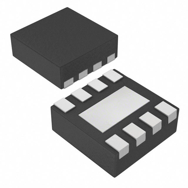
The MCP1501 is available in the following packages:
• 6-Lead SOT-23
• 8-Lead SOIC
• 8-Lead 2 mm x 2 mm WDFN
Package Types
MCP1501
6-Lead SOT-23
OUT 1
6 VDD
GND 2
5 GND
GND 3
4 SHDN
Applications
•
•
•
•
•
Precision Data Acquisition Systems
High-Resolution Data Converters
Medical Equipment Applications
Industrial Controls
Battery-Powered Devices
MCP1501
8-Lead SOIC
VDD 1
8 FEEDBACK
GND 2
7 OUT
SHDN 3
6 GND
GND 4
5 GND
MCP1501
2x2 WDFN*
VDD
1
GND
2
SHDN
3
GND
4
EP
9
8
FEEDBACK
7
OUT
6
GND
5
GND
*Includes Exposed Thermal Pad (EP). See Table 3-1
2015-2017 Microchip Technology Inc.
DS20005474E-page 1
�MCP1501
BLOCK DIAGRAM
VDD
Σ
OUT
FEEDBACK
Shutdown
Circuitry
SHDN
GND
DS20005474E-page 2
2015-2017 Microchip Technology Inc.
�MCP1501
1.0
ELECTRICAL CHARACTERISTICS
Absolute Maximum Ratings(†)
VDD.............................................................................................................................................................................5.5V
Maximum current into VDD pin ............................................................................................................................... 30 mA
Clamp current, IK (VPIN < 0 or VPIN > VDD)........................................................................................................... ±20 mA
Maximum output current sunk by OUTPUT pin ......................................................................................................30 mA
Maximum output current sourced by OUTPUT pin .................................................................................................30 mA
(HBM:CDM:MM)................................................................................................................................ (2 kV:±1.5 kV:200V)
† Notice: Stresses above those listed under “Absolute Maximum Ratings” may cause permanent damage to the
device. This is a stress rating only and functional operation of the device at those or any other conditions above those
indicated in the operation listings of this specification is not implied. Exposure above maximum rating conditions for
extended periods may affect device reliability.
TABLE 1-1:
DC CHARACTERISTICS
Electrical Characteristics: Unless otherwise specified, VDD(MIN) VDD 5.5V at –40C TA +125C.
Characteristic
Supply Voltage
Power-on-Reset
Release Voltage
Power-on-Reset
Rearm Voltage
Output Voltage MCP1501-10
MCP1501-12
MCP1501-18
MCP1501-20
MCP1501-25
MCP1501-30
MCP1501-33
MCP1501-40
Temperature
MCP1501-XX
Coefficient
Line
Regulation
Load
Regulation
Dropout
Voltage
Power Supply
Rejection
Ratio
2015-2017 Microchip Technology Inc.
Sym.
Min.
Typ.
Max.
Units
VDD
VDD
VDD
VDD
VDD
VDD
VDD
VDD
VPOR
1.65
1.65
2.0
2.25
2.70
3.2
3.5
4.3
—
—
—
—
—
—
—
—
—
1.45
5.5
5.5
5.5
5.5
5.5
5.5
5.5
5.5
—
V
V
V
V
V
V
V
V
V
—
—
0.8
—
V
VOUT
1.0230
1.2488
1.7982
2.0460
2.4975
2.9970
3.2967
4.0919
—
1.0240
1.2500
1.800
2.0480
2.500
3.000
3.300
4.0960
10
1.0250
1.2513
1.8018
2.0500
2.5025
3.0030
3.3033
4.1001
50
V
V
V
V
V
V
V
V
ppm/C
VOUT /
VIN
VOUT /
IOUT
—
5
50
ppm/V
VDO
—
TC
PSRR
—
10 ppm – 40 ppm –
sink
sink
15 ppm – 70 ppm –
source
source
—
200
94 dB
Conditions
MCP1501-10
MCP1501-12
MCP1501-18
MCP1501-20
MCP1501-25
MCP1501-30
MCP1501-33
MCP1501-40
ppm/mA –5 mA < ILOAD < +5 mA
mV
–5 mA < ILOAD < +2 mA
1.024V option, VIN = 5.5V,
60 Hz at 100 mVP-P
DS20005474E-page 3
�MCP1501
TABLE 1-1:
DC CHARACTERISTICS (CONTINUED)
Electrical Characteristics: Unless otherwise specified, VDD(MIN) VDD 5.5V at –40C TA +125C.
Characteristic
Sym.
Shutdown
VIL
VIH
Output Voltage
Hysteresis
Output Noise
MCP1501-10
eN
MCP1501-40
eN
TABLE 1-2:
ILOAD
IDD
MCP1501-10
MCP1501-20
MCP1501-40
Typ.
Max.
Units
1.35
3.80
300 µV
∆VOUT_HYST
Maximum
Load Current
Supply
Current
Shutdown
Current
Min.
VIN = 5.5V
—
—
—
—
—
14
27
20
110
±20
—
—
—
—
—
µVRMS
—
—
140
—
205
185
185
550
350
µA
ISHDN
Conditions
µVRMS
mA
nA
Refer to Section 1.1.10
“Output Voltage
Hysteresis” for additional
details on testing conditions.
0.1 Hz to 10 Hz, TA = +25C
10 Hz to 10 kHz, TA = +25C
0.1 Hz to 10 Hz, TA = +25C
10 Hz to 10 kHz, TA = +25C
TA = +25°C
2.048V option
No Load
No Load, TA = +25°C
TA = +25°C
TEMPERATURE SPECIFICATIONS
Electrical Specifications: Unless otherwise indicated, all parameters apply at AVDD, DVDD = 2.7 to 3.6V.
Parameters
Sym.
Min.
Typ.
Max.
Units
Operating Temperature Range
TA
–40
—
+125
°C
Storage Temperature Range
TA
–65
—
+150
°C
Thermal Resistance for SOT-23-6
JA
—
+190.5
—
°C/W
Thermal Resistance for SOIC-8
JA
—
+149.5
—
°C/W
Thermal Resistance for DFN-8
JA
—
+141.3
—
°C/W
Conditions
Temperature Ranges
Thermal Package Resistance
DS20005474E-page 4
2015-2017 Microchip Technology Inc.
�MCP1501
1.1
Terminology
1.1.1
OUTPUT VOLTAGE
Output voltage is the reference voltage that is available
on the OUT pin.
1.1.2
INPUT VOLTAGE
The input voltage (VIN) is the range of voltage that can
be applied to the VDD pin and still have the device
produce the designated output voltage on the OUT pin.
1.1.3
TEMPERATURE COEFFICIENT
(TCOUT)
The output temperature coefficient or voltage drift is a
measure of how much the output voltage will vary from
its initial value with changes in ambient temperature.
The value specified in the electrical specifications is
measured as shown in Equation 1-1.
EQUATION 1-1:
TCOUTPUT CALCULATION
V OUT MAX – V OUT MIN
6
TC OUT = --------------------------------------------------------------------------- 10 ppm/ C
T V OUT NOM
Where:
VOUT(MAX) = Maximum output voltage over the
temperature range
VOUT(MIN) = Minimum output voltage over the
temperature range
VOUT(NOM) = Average output voltage over the
temperature range
T = Temperature range over which the
data was collected
1.1.4
DROPOUT VOLTAGE
The dropout voltage is defined as the voltage difference
between VDD and VOUT under load. Equation 1-2 is
used to calculate the dropout voltage.
EQUATION 1-2:
V DO = V IN – V OUT | I OUT = Cons tan t
1.1.5
EQUATION 1-3:
V OUT
-------------------- 100% = % Line Regulation
V IN
Line regulation may also be expressed as %/V or in
ppm/V, as shown in Equation 1-4 and Equation 1-5,
respectively.
EQUATION 1-4:
V OUT
-----------------------------------
V OUT NOM
%
----------------------------------------- 100% = ----- Line Regulation
V IN
V
EQUATION 1-5:
V OUT
-----------------------------------
V OUT NOM
6
ppm
----------------------------------------- 10 = ----------- Line Regulation
V IN
V
As an example, if the MCP1501-20 is implemented in a
design and a 2 µV change in output voltage is measured from a 250 mV change on the input, then the
error in percent, ppm, percent/volt, and ppm/volt, as
shown in Equation 1-6 – Equation 1-9.
EQUATION 1-6:
V OUT
2 V
-------------------- 100% ------------------ 100% = .0008%
V
250 mV
IN
EQUATION 1-7:
V OUT
6
6
2 V
-------------------- 10 ------------------ 10 = 8 ppm
250 mV
V IN
EQUATION 1-8:
2 V -
--------------- 2.048V
-------------------- 100% = ----------------------- 100% = 0.000390625 %
---- V IN
V
250 mV
V OUT
LINE REGULATION
An ideal voltage reference will maintain a constant output voltage regardless of any changes to the input voltage. However, when real devices are considered, a
small error may be measured on the output when an
input voltage change occurs.
EQUATION 1-9:
2 V -
--------------- V OUT
2.048V
6
6
ppm
------------------- 10 = ----------------------- 10 = 3.90625 ----------- V IN
V
250 mV
Line regulation is defined as the change in output voltage (VOUT) as a function of a change in input voltage
(VIN), and expressed as a percentage, as shown in
Equation 1-3.
2015-2017 Microchip Technology Inc.
DS20005474E-page 5
�MCP1501
1.1.6
LOAD REGULATION
An ideal voltage reference will maintain the specified
output voltage regardless of the load's current demand.
However, real devices experience a small error voltage
that deviates from the specified output voltage when a
load is present.
Load regulation is defined as the voltage difference
when under no load (VOUT @ IOUT|0) and under maximum load (VOUT @ IOUT|MAX), and is expressed as a
percentage, as shown in Equation 1-10.
EQUATION 1-10:
V OUT @ I OUT|0 – V OUT @ I OUT|MAX
-------------------------------------------------------------------------------------------------------------- 100% = % Load Regulation
V OUT @ I OUT|0
Similar to line regulation, load regulation may also be
expressed as %/mA or in ppm/mA as shown in
Equation 1-11 and Equation 1-12, respectively.
EQUATION 1-11:
V OUT
-----------------------------------
V OUT NOM
%
----------------------------------------- 100% = -------- Load Regulation
I OUT
mA
EQUATION 1-16:
V OUT
10 V-
------------------------------------
--------------- V OUT NOM
2.048V
6
6
------------------------------------------ 10 = ----------------------- 10 = 2.441 ppm
---------- I OUT
mA
2 mA
EQUATION 1-12:
V OUT
-----------------------------------
V OUT NOM
6 ppm
----------------------------------------- 10 = ----------- Load Regulation
I OUT
mA
As an example, if the MCP1501-20 is implemented in a
design and a 10 µV change in output voltage is measured from a 2 mA change on the input, then the error
in percent, ppm, percent/volt, ppm/volt, as shown in
Equation 1-13 – Equation 1-16.
EQUATION 1-13:
2.048V
– 2.04799V--------------------------------------------- 100% = . 0004882%
2.04799V
EQUATION 1-14:
6
6
2.048V
– 2.04799V2.048V – 2.04799V
--------------------------------------------- 10 = ----------------------------------------------- 10 = 4.882 ppm
2.04799V
2.04799V
EQUATION 1-15:
V OUT
10 V
------------------------------------
--------------- V OUT NOM
2.048V
%------------------------------------------ 100% = ----------------------- 100% = 0.2441 ------2
mA
I OUT
mA
DS20005474E-page 6
2015-2017 Microchip Technology Inc.
�MCP1501
1.1.7
INPUT CURRENT
The input current (operating current) is the current that
sinks from VIN to GND without a load current on the
output pin. This current is affected by temperature,
input voltage, output voltage, and the load current.
1.1.8
POWER SUPPLY REJECTION
RATIO
Power supply rejection ratio (PSRR) is a measure of
the change in output voltage (∆VOUT) relative to the
change in input voltage (∆VIN) over frequency.
1.1.9
LONG-TERM DRIFT
The long-term output stability is measured by exposing
the devices to an ambient temperature of +125°C, as
shown in Figure 2-18 while configured in the circuit
shown in Figure 1-1. In this test, all electrical specifications of the devices are measured periodically at
+25°C.
Power
VIN
GND
FB
VOUT
Signal In
FIGURE 1-1:
1.1.10
GND
GND
GND
GND
Long-Term Drift Test Circuit.
OUTPUT VOLTAGE HYSTERESIS
The output voltage hysteresis is a measure of the output voltage error after the powered devices are cycled
over the entire operating temperature range. The
amount of hysteresis can be quantified by measuring
the change in the +25°C output voltage after temperature excursions from +25°C to +125°C to +25°C, and
also from +25°C to –40°C to +25°C.
2015-2017 Microchip Technology Inc.
DS20005474E-page 7
�MCP1501
2.0
TYPICAL OPERATING CURVES
Note:
The graphs and tables provided following this note are a statistical summary based on a limited number of
samples and are provided for informational purposes only. The performance characteristics listed herein
are not tested or guaranteed. In some graphs or tables, the data presented may be outside the specified
operating range (e.g., outside specified power supply range) and therefore outside the warranted range.
Note: Unless otherwise specified, maximum values are: VDD(MIN) VDD 5.5V at –40C TA +125C.
40
1.024V
1.8V
2.5V
3.3V
35
Load Reg (ppm/mA)
4.098
Vout (V)
4.097
4.096
4.095
4.094
4.093
4.092
-40
5
25
85
30
1.25V
2.048V
3V
4.096V
25
20
15
10
5
125
0
Temperature (°C)
-40
FIGURE 2-1:
VOUT vs. Temperature, No
Load, 4.096V Option.
1.024V
2.5V
35
Load Reg (ppm/mA)
2.0485
Vout (V)
2.0475
2.047
2.0465
2.046
-40
5
25
85
125
1.25V
3V
1.8V
3.3V
2.048V
4.096V
30
25
20
15
10
5
0
Temperature (°C)
-40
FIGURE 2-2:
VOUT vs. Temperature, No
Load, 2.048V Option.
125
FIGURE 2-4:
Load Regulation vs.
Temperature, ILOAD 5mA Sink.
40
2.048
25
Temperature (°C)
25
Temperature (°C)
125
FIGURE 2-5:
Load Regulation vs.
Temperature, ILOAD 5mA Source.
300
1.0244
1.0242
250
1.024
IDD (µA)
Vout (V)
V287 = 4.096V�
V287�= 2.048V�
V287�= 1.024V
275
1.0238
1.0236
1.0234
1.0232
225
200
175
1.023
-40
5
25
85
125
Temperature (°C)
FIGURE 2-3:
VOUT vs. Temperature, No
Load, 1.024V Option.
DS20005474E-page 8
150
-40
FIGURE 2-6:
Options.
5
25
Temperature (°C)
85
125
IDD vs. Temperature, All
2015-2017 Microchip Technology Inc.
�MCP1501
450
260
Average
+3 Sigma
-3 Sigma
400
350
220
300
200
IDD (µA)
250
200
150
180
160
140
100
120
50
IDD (µA)
200
150
100
Average
+3 Sigma
-3 Sigma
50
Line Reg (ppm/V)
250
0
25
85
125
5
4.5
4
3.5
3
2.5
2
1.5
1
0.5
0
5.5
5
5.25
4.5
4.75
4.25
4
V287 = 1.024V�
V287 = 2.048V�
V287� = 3.3V
-40 -25 -10
Temperature (°C)
FIGURE 2-8:
IDD vs. Temperature for
VOUT, 50 Units, No Load, 1.024V Option.
FIGURE 2-11:
Temperature.
5 20 35 50 65
Temperature (°C)
V287 = 1.25V�
V287 = 2.5V�
V287 = 4.096V
80
V287 = 1.8V
V287 = 3.0V
95 110 125
Line Regulation vs.
1000
350
250
200
150
100
Average
+3 Sigma
-3 Sigma
50
0
4.3
4.45
4.6
4.75
4.9
5.05
5.2
5.5
VDD (V)
FIGURE 2-9:
IDD vs. VDD, VOUT = 4.096V,
50 Units, No Load.
2015-2017 Microchip Technology Inc.
Noise Density (uV/rtHz)
300
IDD (µA)
3.5
FIGURE 2-10:
IDD vs. VDD, VOUT = 1.024V,
50 Units, No Load.
300
5
3
VDD (V)
FIGURE 2-7:
IDD vs. Temperature for
VOUT, 50 Units, No Load, 4.096V Option.
-40
3.75
125
3.25
85
2.5
5
25
Temperature (°C)
2.75
-40
2
1.65
100
0
2.25
IDD (µA)
Average
-3 Sigma
+3 Sigma
240
1.024V
4.096V
100
10
1
0.1
0.01
0.1
10
1000
Frequency (Hz)
100000
FIGURE 2-12:
Noise vs. Frequency, No
Load, TA = +25°C.
DS20005474E-page 9
�MCP1501
120
0.18
0.16
Percentage of Total Units
PSRR (dB)
100
80
60
40
V287 = 1.024, V,1 = 1.65V�
V287 = 1.024V, V,1 = 5.5V�
V287 = 4.096V, V,1 = 4.3V�
V287 = 4.096V, V,1 = 5.5V
20
0
1
10
100
1000
Frequency (Hz)
10000
100000
FIGURE 2-13:
PSRR vs. Frequency, No
Load, TA = +25°C.
0.1
0.08
0.06
0.04
0.02
0
1
0.16
100
0.14
60
40
V287 = 1.024V, V,1 = 1.65V
V287 = 1.024V, V,1 = 5.5V�
V287 = 4.096V, V,1 = 4.3V�
V287 = 4.096V, V,1 = 5.5V
20
0
1
10
100
1000
Frequency (Hz)
10000
0.12
0.1
0.08
0.06
0.04
0.02
0
1
100000
FIGURE 2-14:
PSRR vs. Frequency, 1 kΩ
Load, TA = +25°C.
1
120
0.8
VOUT Drift (mV)
1.2
140
80
60
40
20
3 5 7 9 11 13 15 17 19 21 23 25 27 29
Temperature Coefficient (ppm/&)
FIGURE 2-17:
Tempco Distribution, No
Load, TA = +25°C, VDD = 5.5V, 50 Units.
160
100
3 5 7 9 11 13 15 17 19 21 23 25 27 29
Temperature Coefficient (ppm/&)
FIGURE 2-16:
Tempco Distribution, No
Load, TA = +25°C, VDD = 2.7V, 50 Units.
Percentage of Total Units
PSRR (dB)
0.12
120
80
Dropout Voltage (mV)
0.14
Average
+3 Sigma
-3 Sigma
0.6
0.4
0.2
0
-0.2
-0.4
0
-0.6
-5
-2
0
2
5
Load (mA)
FIGURE 2-15:
Dropout Voltage vs. Load,
TA = +25°C, 2.048V Option.
DS20005474E-page 10
0
48
Time (Hrs)
1008
FIGURE 2-18:
VOUT Drift vs. Time,
TA = +25°C, No Load, 800 Units.
2015-2017 Microchip Technology Inc.
�VOUT (V)
MCP1501
2.0485
2.0484
2.0483
2.0482
2.0481
2.048
2.0479
2.0478
2.0477
2.0476
2.0475
VOUT
2V/div
500 µs/div
VIN
2V/div
500 µs/div
-20
-10
0
10
Conditions:
20
Load (mA)
VOUT vs. Load, TA = +25°C,
FIGURE 2-19:
2.048V Option.
FIGURE 2-22:
Turn On Transient,
VDD = 5/5V, VIN = 2.048V Option, No Load.
Percentage of Total Units
0.7
VIN
1V/div
5 ms/div
0.6
QC +25°C
0.5
QC -40°C
0.4
QC +125°C
0.3
VOUT
10 mV /div
5 ms/div
0.2
0.1
0
Conditions:
VOUT (V)
FIGURE 2-20:
VOUT at VDDMIN,
VDD = 2.7V, 800 Units, 2.5V Option, No Load.
FIGURE 2-23:
Line Transient, VDD = 5.5V,
VIN = 500 mVPP @ 5VDC, 2.048V Option, No
Load.
Percentage of Total Units
0.7
0.6
QC +25°C
0.5
QC -40°C
0.4
IOUT
10 mA/div
QC +125°C
0.3
0.2
0.1
0
2.495
2.496
2.497
2.498
2.499
2.500
2.501
2.502
2.503
2.504
VOUT
500 mV/div
200 µs/div
VOUT (V)
FIGURE 2-21:
VOUT Distribution at
VDDMAX, VDD = 5.5V, 800 Units, 2.5V Option, No
Load.
2015-2017 Microchip Technology Inc.
FIGURE 2-24:
Load Transient, VDD = 5.5,
VIN = 2.5, 2.048V Option.
DS20005474E-page 11
�MCP1501
3KDVH�0DUJLQ���
135
1Ω
10Ω
100Ω
1 kΩ
90
45
0
&DSDFLWLYH�/RDG��)�
FIGURE 2-25:
Option Unloaded.
RISO vs. CLOAD, 4.096V
135
1Ω
10Ω
100Ω
1 kΩ
Capactive Load
90
45
0
Phase Margin (°)
FIGURE 2-26:
Option Loaded.
DS20005474E-page 12
RISO vs. CLOAD, 4.096V
2015-2017 Microchip Technology Inc.
�MCP1501
3.0
PIN FUNCTION TABLE
The pin functions are described in Table 3-1.
TABLE 3-1:
PIN FUNCTION TABLE
SOT-23
SOIC
2 x 2 WDFN
Symbol
1
7
7
OUT
—
8
8
FEEDBACK
2, 3, 5
2, 4, 5, 6
2, 4, 5, 6
GND
4
3
3
SHDN
6
1
1
VDD
Power Supply Input
—
—
9
EP
Exposed Thermal Pad
3.1
Function
Buffered VREF Output
Buffered VREF Feedback
System Ground
Shutdown Pin Active Low
Buffered VREF Output (OUT)
This is the Buffered Reference Output. On the WDFN
and SOIC package, this should be connected to the
FEEDBACK pin at the device. The output driver is
tristated when in shutdown.
3.2
Buffered VREF Feedback
(FEEDBACK)
This is the buffer amplifier feedback pin. On the WDFN
and SOIC package, this should be connected to the
OUT pin at the device. This connection is internal on
the SOT-23 package. Note that if there is routing
impedance or IR-drop between the OUT and
FEEDBACK pins, it is the FEEDBACK pin which accurately holds the output voltage. This can be used in an
application to remove IR-drop effects on output voltage
caused by the Printed Circuit Board (PCB) or
interconnect resistance with a high-current load.
3.3
System Ground (GND)
This is the power supply return and should be
connected to system ground.
3.4
Shutdown Pin (SHDN)
This is a digital input that will place the device in
Shutdown. The device should be allowed to power up
before using this feature. This pin is active low.
3.5
Power Supply Input (VDD)
This power pin also serves as the input voltage for the
voltage reference. Refer to the Electrical Tables to
determine minimum voltage, based on the device.
3.6
Exposed Thermal Pad (EP)
Not internally connected, but recommend grounding.
2015-2017 Microchip Technology Inc.
DS20005474E-page 13
�MCP1501
4.0
THEORY OF OPERATION
The MCP1501 is a buffered voltage reference that is
capable of operating over a wide input supply range
while providing a stable output across the input supply
range. The fundamental building block (see Block Diagram) of the MCP1501 is an internal bandgap reference circuit. As with all bandgap circuits, the internal
reference sums together two voltages having an opposite temperature coefficient which allows a voltage reference that is practically independent from
temperature.
The bandgap of the MCP1501 is based on a second
order temperature coefficient (TC) compensated bandgap circuit that allows the MCP1501 to achieve high initial accuracy and low temperature coefficient operation
across supply and ambient temperature. The bandgap
curvature compensation is determined during device
characterization and is trimmed for optimal accuracy.
The MCP1501 also includes a chopper-based amplifier
architecture that ensures excellent low-noise operation, further reduces temperature dependent offsets
that would otherwise increase the temperature coefficient of the MCP1501, and significantly improves
long-term drift performance. Additional circuitry is
included to eliminate the chopping frequency from the
output of the device.
After the bandgap voltage is compensated, it is amplified, buffered, and provided to the output drive circuit
which has excellent performance when sinking or
sourcing load currents (±5 mA).
DS20005474E-page 14
2015-2017 Microchip Technology Inc.
�MCP1501
5.0
APPLICATION CIRCUITS
5.1
Application Tips
5.1.1
BASIC APPLICATION CIRCUIT
Figure 5-1 illustrates a basic circuit configuration of the
MCP1501.
1.65 – 5.5V
1
VDD FEEDBACK
8
2
GND
OUT
7
3
SHDN
GND
6
4
GND
GND
5
OUT
300 SF
0.1 – 2.2 μF
SOIC-8/DFN-8
FIGURE 5-1:
Basic Circuit Configuration.
An output capacitor is not required for stability of the
voltage reference, but may be optionally added to provide noise filtering or act as a charge-reservoir for
switching loads, e.g., successive approximation register (SAR) analog-to-digital converter (ADC). As shown,
the input voltage is connected to the device at the VIN
input, with an optional 2.2 μf ceramic capacitor. This
capacitor would be required if the input voltage has
excessive noise. A 2.2 μf capacitor would reject input
voltage noise at approximately 1 to 2 MHz. Noise
below this frequency will be amply rejected by the input
voltage rejection of the voltage reference. Noise at frequencies above 2 MHz will be beyond the bandwidth of
the voltage reference and, consequently, not transmitted from the input pin through the device to the output.
If the noise at the output of these voltage references is
too high for the particular application, it can be easily filtered with an external RC filter and op-amp buffer (see
Figure 5-2).
RFIL
Output
of V
REF
CFIL
FIGURE 5-2:
Filter.
Output Noise-Reducing
2015-2017 Microchip Technology Inc.
DS20005474E-page 15
�MCP1501
The RC filter values are selected for a desired cutoff
frequency, as shown in Equation 5-1.
EQUATION 5-1:
1
f C = --------------------------------------2 R FIL C FIL
The values that are shown in Figure 5-2 (10 kΩ and
1 μF) will create a first-order, low-pass filter at the output of the amplifier. The cutoff frequency of this filter is
15.9 Hz, and the attenuation slope is 20 dB/decade.
The MCP6021 amplifier isolates the loading of this lowpass filter from the remainder of the application circuit.
This amplifier also provides additional drive, with a
faster response time than the voltage reference.
5.1.2
LOAD CAPACITOR
The maximum capacitive load is 300 pF. However,
larger capacitors may be implemented if a resistor is
used in series with a larger load capacitor. Refer to
Figure 2-25 and Figure 2-26 to ensure adequate phase
margin
when
selecting
a
resistor/capacitor
combination.
5.1.3
PRINTED CIRCUIT BOARD LAYOUT
CONSIDERATIONS
Mechanical stress due to Printed Circuit Board (PCB)
mounting can cause the output voltage to shift from its
initial value. Devices in the SOT-23-6 package are generally more prone to assembly stress than devices in
the WDFN package. To reduce stress-related output
voltage shifts, mount the reference on low-stress areas
of the PCB (i.e., away from PCB edges, screw holes
and large components).
DS20005474E-page 16
2015-2017 Microchip Technology Inc.
�MCP1501
5.2
5.2.1
Since the noninverting input of the amplifier is biased to
ground, the inverting input will also be close to ground
potential. The second 10 kΩresistor is placed around
the feedback loop of the amplifier. Since the inverting
input of the amplifier is high-impedance, the current
generated through R1 will also flow through R2. As a
consequence, the output voltage of the amplifier is
equal to –2.5V for the MCP1501-25 and –4.096V for
the MCP1501-40.
Typical Applications Circuits
NEGATIVE VOLTAGE REFERENCE
A negative voltage reference can be generated using
any of the devices in the MCP1501 family. A typical
application is shown in Figure 5-3. In this circuit, the
voltage inversion is implemented using the MCP6061
and two equal resistors. The voltage at the output of the
MCP1501 voltage reference drives R1, which is connected to the inverting input of the MCP6061 amplifier.
MCP1501-;;
2.7 – 5.5V
10 kΩ
0.1%
1
VDD FEEDBACK
8
2
GND
OUT
7
3
SHDN
GND
6
4
GND
GND
5
10 kΩ
0.1%
-2.500V
2.2 μF
+
1 nF
-5V
MCP6061
FIGURE 5-3:
5.2.2
Negative Voltage Reference.
A/D CONVERTER REFERENCE
The MCP1501 product family was carefully designed to
provide a precision, low noise voltage reference for the
Microchip families of ADCs. The circuit shown in
Figure 5-4 shows a MCP1501-25 configured to provide
the reference to the MCP3201, a 12-bit ADC.
1
VDD FEEDBACK
8
2
GND
OUT
7
3
SHDN
GND
6
4
GND
GND
5
50Ω
MCP1501-;;
5.0V
2.2 μF
2.2 μF
5.0V
VREF
VIN
IN+
MCP3201
0.1 μF
10 μF
IN-
FIGURE 5-4:
ADC Example Circuit.
2015-2017 Microchip Technology Inc.
DS20005474E-page 17
�MCP1501
MCP1501-25
5.0V
FEEDBACK
10Ω
VDD
GND
OUT
SHDN
GND
GND
GND
10 kΩ
2.2 μF
2.2 μF (Ta)
5.0V
VIN
IN+
14/16-bit
SAR ADC
IN-
FIGURE 5-5:
0.1 μF
10 μF
SAR ADC Example Circuit.
The circuit shown in Figure 5-5 shows a MCP1501-25
configured to provide the reference to a 14-bit or 16-bit
SAR ADC.
DS20005474E-page 18
2015-2017 Microchip Technology Inc.
�MCP1501
6.0
PACKAGE INFORMATION
6.1
Package Markings
Example
6-Lead SOT-23
Device
XXXXY
XXNN
WWNNN
Code
MCP1501T-10E/CHY
AABTY
MCP1501T-12E/CHY
AABUY
MCP1501T-18E/CHY
AABVY
MCP1501T-20E/CHY
AABWY
MCP1501T-25E/CHY
AABXY
MCP1501T-30E/CHY
AABYY
MCP1501T-33E/CHY
AABZY
MCP1501T-40E/CHY
AACAY
8-Lead SOIC
Example
Device
MCP1501T-10E/SN
NNN
Code
150110
MCP1501T-12E/SN
150112
MCP1501-18E/SN
150118
MCP1501-20E/SN
150120
MCP1501T-25E/SN
150125
MCP1501T-30E/SN
150130
MCP1501T-33E/SN
150133
MCP1501T-40E/SN
150140
8-Lead WDFN (2 x2 mm)
Legend: XX...X
Y
YY
WW
NNN
e3
*
Note:
AABTY
50256
150110
SN^^^1550
e3
256
Example
Device
Code
MCP1501T-10E/RW
AAQ
MCP1501T-12E/RW
AAR
MCP1501-18E/RW
AAS
MCP1501-20E/RW
AAT
MCP1501T-25E/RW
AAU
MCP1501T-30E/RW
AAV
MCP1501T-33E/RW
AAW
MCP1501T-40E/RW
AAX
AAQ
256
Customer-specific information
Year code (last digit of calendar year)
Year code (last 2 digits of calendar year)
Week code (week of January 1 is week ‘01’)
Alphanumeric traceability code
Pb-free JEDEC® designator for Matte Tin (Sn)
This package is Pb-free. The Pb-free JEDEC designator ( e3 )
can be found on the outer packaging for this package.
In the event the full Microchip part number cannot be marked on one line, it will
be carried over to the next line, thus limiting the number of available
characters for customer-specific information.
2015-2017 Microchip Technology Inc.
DS20005474E-page 19
�MCP1501
6-Lead Plastic Small Outline Transistor (CH, CHY) [SOT-23]
Note:
For the most current package drawings, please see the Microchip Packaging Specification located at
http://www.microchip.com/packaging
2X
0.15 C A-B
D
e1
A
D
E
2
E1
E
E1
2
2X
0.15 C D
2X
0.20 C A-B
e
6X b
B
0.20
C A-B D
TOP VIEW
C
A
A2
SEATING PLANE
6X
A1
0.10 C
SIDE VIEW
R1
L2
R
c
GAUGE PLANE
L
Ĭ
(L1)
END VIEW
Microchip Technology Drawing C04-028C (CH) Sheet 1 of 2
DS20005474E-page 20
2015-2017 Microchip Technology Inc.
�MCP1501
6-Lead Plastic Small Outline Transistor (OT, OTY) [SOT-23]
Note:
For the most current package drawings, please see the Microchip Packaging Specification located at
http://www.microchip.com/packaging
Units
Dimension Limits
N
Number of Leads
e
Pitch
Outside lead pitch
e1
Overall Height
A
Molded Package Thickness
A2
Standoff
A1
Overall Width
E
Molded Package Width
E1
Overall Length
D
Foot Length
L
Footprint
L1
Seating Plane to Gauge Plane
L1
φ
Foot Angle
c
Lead Thickness
Lead Width
b
MIN
0.90
0.89
0.00
0.30
0°
0.08
0.20
MILLIMETERS
NOM
6
0.95 BSC
1.90 BSC
1.15
2.80 BSC
1.60 BSC
2.90 BSC
0.45
0.60 REF
0.25 BSC
-
MAX
1.45
1.30
0.15
0.60
10°
0.26
0.51
Notes:
1. Dimensions D and E1 do not include mold flash or protrusions. Mold flash or
protrusions shall not exceed 0.25mm per side.
2. Dimensioning and tolerancing per ASME Y14.5M
BSC: Basic Dimension. Theoretically exact value shown without tolerances.
REF: Reference Dimension, usually without tolerance, for information purposes only.
Microchip Technology Drawing C04-028C (OT) Sheet 2 of 2
2015-2017 Microchip Technology Inc.
DS20005474E-page 21
�MCP1501
8-Lead Plastic Small Outline (SN) - Narrow, 3.90 mm (.150 In.) Body [SOIC]
Note:
For the most current package drawings, please see the Microchip Packaging Specification located at
http://www.microchip.com/packaging
2X
0.10 C A–B
D
A
D
NOTE 5
N
E
2
E1
2
E1
E
NOTE 1
2
1
e
B
NX b
0.25
C A–B D
NOTE 5
TOP VIEW
0.10 C
C
A A2
SEATING
PLANE
8X
A1
SIDE VIEW
0.10 C
h
R0.13
h
R0.13
H
SEE VIEW C
VIEW A–A
0.23
L
(L1)
VIEW C
Microchip Technology Drawing No. C04-057-SN Rev D Sheet 1 of 2
DS20005474E-page 22
2015-2017 Microchip Technology Inc.
�MCP1501
8-Lead Plastic Small Outline (SN) - Narrow, 3.90 mm (.150 In.) Body [SOIC]
Note:
For the most current package drawings, please see the Microchip Packaging Specification located at
http://www.microchip.com/packaging
Units
Dimension Limits
Number of Pins
N
e
Pitch
Overall Height
A
Molded Package Thickness
A2
§
Standoff
A1
Overall Width
E
Molded Package Width
E1
Overall Length
D
Chamfer (Optional)
h
Foot Length
L
L1
Footprint
Foot Angle
c
Lead Thickness
b
Lead Width
Mold Draft Angle Top
Mold Draft Angle Bottom
MIN
1.25
0.10
0.25
0.40
0°
0.17
0.31
5°
5°
MILLIMETERS
NOM
8
1.27 BSC
6.00 BSC
3.90 BSC
4.90 BSC
1.04 REF
-
MAX
1.75
0.25
0.50
1.27
8°
0.25
0.51
15°
15°
Notes:
1. Pin 1 visual index feature may vary, but must be located within the hatched area.
2. § Significant Characteristic
3. Dimensions D and E1 do not include mold flash or protrusions. Mold flash or
protrusions shall not exceed 0.15mm per side.
4. Dimensioning and tolerancing per ASME Y14.5M
BSC: Basic Dimension. Theoretically exact value shown without tolerances.
REF: Reference Dimension, usually without tolerance, for information purposes only.
5. Datums A & B to be determined at Datum H.
Microchip Technology Drawing No. C04-057-SN Rev D Sheet 2 of 2
2015-2017 Microchip Technology Inc.
DS20005474E-page 23
�MCP1501
8-Lead Plastic Small Outline (SN) - Narrow, 3.90 mm Body [SOIC]
Note:
For the most current package drawings, please see the Microchip Packaging Specification located at
http://www.microchip.com/packaging
SILK SCREEN
C
Y1
X1
E
RECOMMENDED LAND PATTERN
Units
Dimension Limits
E
Contact Pitch
Contact Pad Spacing
C
Contact Pad Width (X8)
X1
Contact Pad Length (X8)
Y1
MIN
MILLIMETERS
NOM
1.27 BSC
5.40
MAX
0.60
1.55
Notes:
1. Dimensioning and tolerancing per ASME Y14.5M
BSC: Basic Dimension. Theoretically exact value shown without tolerances.
Microchip Technology Drawing C04-2057-SN Rev B
DS20005474E-page 24
2015-2017 Microchip Technology Inc.
�MCP1501
8-Lead Very, Very Thin Plastic Dual Flat, No Lead Package (RW) - 2x2 mm Body [WDFN]
Note:
For the most current package drawings, please see the Microchip Packaging Specification located at
http://www.microchip.com/packaging
D
A
B
N
(DATUM A)
(DATUM B)
E
NOTE 1
2X
0.05 C
1
2X
2
TOP VIEW
0.05 C
0.05 C
C
(A3)
A
SEATING
PLANE
SIDE VIEW
A1
0.05 C
D2
2X CH
1
2
NOTE 1
0.05
C A B
E2
(K)
L
N
8X b
e
BOTTOM VIEW
0.10
0.05
C A B
C
Microchip Technology Drawing C04-261A Sheet 1 of 2
2015-2017 Microchip Technology Inc.
DS20005474E-page 25
�MCP1501
8-Lead Very, Very Thin Plastic Dual Flat, No Lead Package (RW) - 2x2 mm Body [WDFN]
Note:
For the most current package drawings, please see the Microchip Packaging Specification located at
http://www.microchip.com/packaging
Units
Dimension Limits
Number of Terminals
N
e
Pitch
Overall Height
A
Standoff
A1
(A3)
Terminal Thickness
Overall Width
E
Exposed Pad Width
E2
Overall Length
D
Exposed Pad Length
D2
Exposed Pad Chamfer
CH
Terminal Width
b
Terminal Length
L
(K)
Terminal-to-Exposed-Pad
MIN
0.70
0.00
0.70
1.10
0.20
0.25
0.30
MILLIMETERS
NOM
8
0.50 BSC
0.75
0.02
0.10 REF
2.00 BSC
0.80
2.00 BSC
1.20
0.25
0.25
0.30
-
MAX
0.80
0.05
0.90
1.30
0.30
0.35
-
Notes:
1. Pin 1 visual index feature may vary, but must be located within the hatched area.
2. Package is saw singulated
3. Dimensioning and tolerancing per ASME Y14.5M
BSC: Basic Dimension. Theoretically exact value shown without tolerances.
REF: Reference Dimension, usually without tolerance, for information purposes only.
Microchip Technology Drawing C04-261A Sheet 2 of 2
DS20005474E-page 26
2015-2017 Microchip Technology Inc.
�MCP1501
8-Lead Very, Very Thin Plastic Dual Flat, No Lead Package (RW) - 2x2 mm Body [WDFN]
Note:
For the most current package drawings, please see the Microchip Packaging Specification located at
http://www.microchip.com/packaging
C
2X CH
ØV
8
1
2
E
X2
X1
G
SILK SCREEN
(G2)
Y2
Y1
RECOMMENDED LAND PATTERN
Units
Dimension Limits
E
Contact Pitch
Optional Center Pad Width
Y2
Optional Center Pad Length
X2
Contact Pad Spacing
C
Center Pad Chamfer
CH
Contact Pad Width (X8)
X1
Contact Pad Length (X8)
Y1
Contact Pad to Contact Pad (X6)
G1
Contact Pad to Center Pad (X8)
G1
Thermal Via Diameter
V
MIN
MILLIMETERS
NOM
0.50 BSC
MAX
0.90
1.30
2.10
0.28
0.30
0.70
0.20
0.25 REF
0.30
Notes:
1. Dimensioning and tolerancing per ASME Y14.5M
BSC: Basic Dimension. Theoretically exact value shown without tolerances.
REF: Reference Dimension, usually without tolerances, for reference only.
Microchip Technology Drawing C04-2261A
2015-2017 Microchip Technology Inc.
DS20005474E-page 27
�MCP1501
NOTES:
DS20005474E-page 28
2015-2017 Microchip Technology Inc.
�MCP1501
APPENDIX A:
REVISION HISTORY
Revision E (August 2017)
Revision A (December 2015)
The following is the list of modifications:
Original Release of this Document.
• Updated Features.
• Updated Package Types.
• Updated Section 1.0, Electrical Characteristics,
Table 1-1.
• Updated Figure 2-12, Figure 2-20 and Figure 2-21.
• Updated Table 3-1.
• Updated Section 3.4, Shutdown Pin (SHDN).
• Updated Section 5.1.2, LOAD CAPACITOR.
• Corrected Figure 5-3 and Figure 5-4.
• Added Figure 5-5.
• Minor typographical corrections.
Revision D (March 2017)
The following is the list of modifications:
• Updated Table 1-1.
• Updated Equation 1-1, Equation 1-4, Equation 1-5,
Equation 1-10, Equation 1-11, Equation 1-12 and
Equation 1-16.
• Updated Figure 2-11, Figure 2-20, Figure 2-21,
Figure 2-25 and Figure 2-26.
• Updated Figure 5-1 and Figure 5-4.
• Updated “Product Identification System” section.
• Minor typographical corrections.
Revision C (May 2016)
The following is the list of modifications:
• Updated Section 1.0, Electrical Characteristics,
Section 4.0, Theory of Operation, Section 5.0,
Application Circuits.
• Updated Features section, General Description
section, Section 3.1, Buffered VREF Output
(OUT).
• Updated“Product Identification System”
section.
• Updated Figure 2-12, Figure 2-20,
Figure 2-21, Figure 5-1 and Figure 5-4.
• Updated Equation 1-10 and Equation 1-16.
• Minor typographical corrections.
Revision B (January 2016)
The following is the list of modifications:
• Updated Section 6.0, Package Information.
• Updated “Product Identification System”
section.
• Minor typographical corrections.
2015-2017 Microchip Technology Inc.
DS20005474E-page 29
�MCP1501
NOTES:
DS20005474E-page 30
2015-2017 Microchip Technology Inc.
�MCP1501
PRODUCT IDENTIFICATION SYSTEM
To order or obtain information, e.g., on pricing or delivery, refer to the factory or the listed sales office.
[X](1)
PART NO.Device
Tape and
Reel
X
Output Voltage
Option
/XX
Package
Device:
MCP1501 – 50 ppm maximum thermal drift buffered reference
Tape and Reel
Option:
Blank = Standard packaging (tube or tray)
T
= Tape and Reel (1)
Output Voltage
Option:
10
12
18
20
25
30
33
40
=
=
=
=
=
=
=
=
1.024V
1.200V
1.800V
2.048V
2.500V
3.000V
3.300V
4.096V
Package:
CHY*
SN
=
=
RW
=
6-Lead Plastic Small Outline Transistor (SOT-23)
8-Lead Plastic Small Outline – Narrow, 3.90 mm
Body (SOIC)
8-Lead Very, Very Thin Plastic Dual Flat, No Lead
Package – 2 x 2 mm Body (WDFN)
*Y
=
Nickel palladium gold manufacturing designator.
Only available on the SOT-23 package.
2015-2017 Microchip Technology Inc.
Examples:
a)
MCP1501T-10E/CHY: 1.024V, 6-lead SOT-23
package, Tape and Reel
b)
MCP1501-12E/SN:
1.2V, 8-lead SOIC package
c)
MCP1501T-18E/SN:
1.8V, 8-lead SOIC package,
Tape and Reel
d)
MCP1501T-20E/RW:
2.048V, 8-lead WDFN
package, Tape and Reel
Note
1:
Tape and Reel identifier only appears in
the catalog part number description.
This identifier is used for ordering purposes and is not printed on the device
package. Check with your Microchip
sales office for package availability for
the Tape and Reel option.
DS20005474E-page 31
�MCP1501
NOTES:
DS20005474E-page 32
2015-2017 Microchip Technology Inc.
�Note the following details of the code protection feature on Microchip devices:
•
Microchip products meet the specification contained in their particular Microchip Data Sheet.
•
Microchip believes that its family of products is one of the most secure families of its kind on the market today, when used in the
intended manner and under normal conditions.
•
There are dishonest and possibly illegal methods used to breach the code protection feature. All of these methods, to our
knowledge, require using the Microchip products in a manner outside the operating specifications contained in Microchip’s Data
Sheets. Most likely, the person doing so is engaged in theft of intellectual property.
•
Microchip is willing to work with the customer who is concerned about the integrity of their code.
•
Neither Microchip nor any other semiconductor manufacturer can guarantee the security of their code. Code protection does not
mean that we are guaranteeing the product as “unbreakable.”
Code protection is constantly evolving. We at Microchip are committed to continuously improving the code protection features of our
products. Attempts to break Microchip’s code protection feature may be a violation of the Digital Millennium Copyright Act. If such acts
allow unauthorized access to your software or other copyrighted work, you may have a right to sue for relief under that Act.
Information contained in this publication regarding device
applications and the like is provided only for your convenience
and may be superseded by updates. It is your responsibility to
ensure that your application meets with your specifications.
MICROCHIP MAKES NO REPRESENTATIONS OR
WARRANTIES OF ANY KIND WHETHER EXPRESS OR
IMPLIED, WRITTEN OR ORAL, STATUTORY OR
OTHERWISE, RELATED TO THE INFORMATION,
INCLUDING BUT NOT LIMITED TO ITS CONDITION,
QUALITY, PERFORMANCE, MERCHANTABILITY OR
FITNESS FOR PURPOSE. Microchip disclaims all liability
arising from this information and its use. Use of Microchip
devices in life support and/or safety applications is entirely at
the buyer’s risk, and the buyer agrees to defend, indemnify and
hold harmless Microchip from any and all damages, claims,
suits, or expenses resulting from such use. No licenses are
conveyed, implicitly or otherwise, under any Microchip
intellectual property rights unless otherwise stated.
Microchip received ISO/TS-16949:2009 certification for its worldwide
headquarters, design and wafer fabrication facilities in Chandler and
Tempe, Arizona; Gresham, Oregon and design centers in California
and India. The Company’s quality system processes and procedures
are for its PIC® MCUs and dsPIC® DSCs, KEELOQ® code hopping
devices, Serial EEPROMs, microperipherals, nonvolatile memory and
analog products. In addition, Microchip’s quality system for the design
and manufacture of development systems is ISO 9001:2000 certified.
QUALITY MANAGEMENT SYSTEM
CERTIFIED BY DNV
== ISO/TS 16949 ==
2015-2017 Microchip Technology Inc.
Trademarks
The Microchip name and logo, the Microchip logo, AnyRate, AVR,
AVR logo, AVR Freaks, BeaconThings, BitCloud, CryptoMemory,
CryptoRF, dsPIC, FlashFlex, flexPWR, Heldo, JukeBlox, KEELOQ,
KEELOQ logo, Kleer, LANCheck, LINK MD, maXStylus,
maXTouch, MediaLB, megaAVR, MOST, MOST logo, MPLAB,
OptoLyzer, PIC, picoPower, PICSTART, PIC32 logo, Prochip
Designer, QTouch, RightTouch, SAM-BA, SpyNIC, SST, SST
Logo, SuperFlash, tinyAVR, UNI/O, and XMEGA are registered
trademarks of Microchip Technology Incorporated in the U.S.A.
and other countries.
ClockWorks, The Embedded Control Solutions Company,
EtherSynch, Hyper Speed Control, HyperLight Load, IntelliMOS,
mTouch, Precision Edge, and Quiet-Wire are registered
trademarks of Microchip Technology Incorporated in the U.S.A.
Adjacent Key Suppression, AKS, Analog-for-the-Digital Age, Any
Capacitor, AnyIn, AnyOut, BodyCom, chipKIT, chipKIT logo,
CodeGuard, CryptoAuthentication, CryptoCompanion,
CryptoController, dsPICDEM, dsPICDEM.net, Dynamic Average
Matching, DAM, ECAN, EtherGREEN, In-Circuit Serial
Programming, ICSP, Inter-Chip Connectivity, JitterBlocker,
KleerNet, KleerNet logo, Mindi, MiWi, motorBench, MPASM, MPF,
MPLAB Certified logo, MPLIB, MPLINK, MultiTRAK, NetDetach,
Omniscient Code Generation, PICDEM, PICDEM.net, PICkit,
PICtail, PureSilicon, QMatrix, RightTouch logo, REAL ICE, Ripple
Blocker, SAM-ICE, Serial Quad I/O, SMART-I.S., SQI,
SuperSwitcher, SuperSwitcher II, Total Endurance, TSHARC,
USBCheck, VariSense, ViewSpan, WiperLock, Wireless DNA, and
ZENA are trademarks of Microchip Technology Incorporated in the
U.S.A. and other countries.
SQTP is a service mark of Microchip Technology Incorporated in
the U.S.A.
Silicon Storage Technology is a registered trademark of Microchip
Technology Inc. in other countries.
GestIC is a registered trademark of Microchip Technology
Germany II GmbH & Co. KG, a subsidiary of Microchip Technology
Inc., in other countries.
All other trademarks mentioned herein are property of their
respective companies.
© 2015-2017, Microchip Technology Incorporated, All Rights
Reserved.
ISBN: 978-1-5224-2100-9
DS20005474E-page 33
�Worldwide Sales and Service
AMERICAS
ASIA/PACIFIC
ASIA/PACIFIC
EUROPE
Corporate Office
2355 West Chandler Blvd.
Chandler, AZ 85224-6199
Tel: 480-792-7200
Fax: 480-792-7277
Technical Support:
http://www.microchip.com/
support
Web Address:
www.microchip.com
Asia Pacific Office
Suites 3707-14, 37th Floor
Tower 6, The Gateway
Harbour City, Kowloon
China - Xiamen
Tel: 86-592-2388138
Fax: 86-592-2388130
Austria - Wels
Tel: 43-7242-2244-39
Fax: 43-7242-2244-393
China - Zhuhai
Tel: 86-756-3210040
Fax: 86-756-3210049
Denmark - Copenhagen
Tel: 45-4450-2828
Fax: 45-4485-2829
India - Bangalore
Tel: 91-80-3090-4444
Fax: 91-80-3090-4123
Finland - Espoo
Tel: 358-9-4520-820
Atlanta
Duluth, GA
Tel: 678-957-9614
Fax: 678-957-1455
Hong Kong
Tel: 852-2943-5100
Fax: 852-2401-3431
Australia - Sydney
Tel: 61-2-9868-6733
Fax: 61-2-9868-6755
China - Beijing
Tel: 86-10-8569-7000
Fax: 86-10-8528-2104
Austin, TX
Tel: 512-257-3370
China - Chengdu
Tel: 86-28-8665-5511
Fax: 86-28-8665-7889
Boston
Westborough, MA
Tel: 774-760-0087
Fax: 774-760-0088
China - Chongqing
Tel: 86-23-8980-9588
Fax: 86-23-8980-9500
Chicago
Itasca, IL
Tel: 630-285-0071
Fax: 630-285-0075
Dallas
Addison, TX
Tel: 972-818-7423
Fax: 972-818-2924
Detroit
Novi, MI
Tel: 248-848-4000
Houston, TX
Tel: 281-894-5983
Indianapolis
Noblesville, IN
Tel: 317-773-8323
Fax: 317-773-5453
Tel: 317-536-2380
Los Angeles
Mission Viejo, CA
Tel: 949-462-9523
Fax: 949-462-9608
Tel: 951-273-7800
Raleigh, NC
Tel: 919-844-7510
New York, NY
Tel: 631-435-6000
San Jose, CA
Tel: 408-735-9110
Tel: 408-436-4270
Canada - Toronto
Tel: 905-695-1980
Fax: 905-695-2078
DS20005474E-page 34
China - Dongguan
Tel: 86-769-8702-9880
China - Guangzhou
Tel: 86-20-8755-8029
China - Hangzhou
Tel: 86-571-8792-8115
Fax: 86-571-8792-8116
China - Hong Kong SAR
Tel: 852-2943-5100
Fax: 852-2401-3431
China - Nanjing
Tel: 86-25-8473-2460
Fax: 86-25-8473-2470
China - Qingdao
Tel: 86-532-8502-7355
Fax: 86-532-8502-7205
China - Shanghai
Tel: 86-21-3326-8000
Fax: 86-21-3326-8021
China - Shenyang
Tel: 86-24-2334-2829
Fax: 86-24-2334-2393
China - Shenzhen
Tel: 86-755-8864-2200
Fax: 86-755-8203-1760
France - Paris
Tel: 33-1-69-53-63-20
Fax: 33-1-69-30-90-79
India - New Delhi
Tel: 91-11-4160-8631
Fax: 91-11-4160-8632
France - Saint Cloud
Tel: 33-1-30-60-70-00
India - Pune
Tel: 91-20-3019-1500
Germany - Garching
Tel: 49-8931-9700
Germany - Haan
Tel: 49-2129-3766400
Japan - Osaka
Tel: 81-6-6152-7160
Fax: 81-6-6152-9310
Japan - Tokyo
Tel: 81-3-6880- 3770
Fax: 81-3-6880-3771
Germany - Heilbronn
Tel: 49-7131-67-3636
Germany - Karlsruhe
Tel: 49-721-625370
Korea - Daegu
Tel: 82-53-744-4301
Fax: 82-53-744-4302
Germany - Munich
Tel: 49-89-627-144-0
Fax: 49-89-627-144-44
Korea - Seoul
Tel: 82-2-554-7200
Fax: 82-2-558-5932 or
82-2-558-5934
Germany - Rosenheim
Tel: 49-8031-354-560
Malaysia - Kuala Lumpur
Tel: 60-3-6201-9857
Fax: 60-3-6201-9859
Malaysia - Penang
Tel: 60-4-227-8870
Fax: 60-4-227-4068
Philippines - Manila
Tel: 63-2-634-9065
Fax: 63-2-634-9069
Singapore
Tel: 65-6334-8870
Fax: 65-6334-8850
Taiwan - Hsin Chu
Tel: 886-3-5778-366
Fax: 886-3-5770-955
Taiwan - Kaohsiung
Tel: 886-7-213-7830
China - Wuhan
Tel: 86-27-5980-5300
Fax: 86-27-5980-5118
Taiwan - Taipei
Tel: 886-2-2508-8600
Fax: 886-2-2508-0102
China - Xian
Tel: 86-29-8833-7252
Fax: 86-29-8833-7256
Thailand - Bangkok
Tel: 66-2-694-1351
Fax: 66-2-694-1350
Israel - Ra’anana
Tel: 972-9-744-7705
Italy - Milan
Tel: 39-0331-742611
Fax: 39-0331-466781
Italy - Padova
Tel: 39-049-7625286
Netherlands - Drunen
Tel: 31-416-690399
Fax: 31-416-690340
Norway - Trondheim
Tel: 47-7289-7561
Poland - Warsaw
Tel: 48-22-3325737
Romania - Bucharest
Tel: 40-21-407-87-50
Spain - Madrid
Tel: 34-91-708-08-90
Fax: 34-91-708-08-91
Sweden - Gothenberg
Tel: 46-31-704-60-40
Sweden - Stockholm
Tel: 46-8-5090-4654
UK - Wokingham
Tel: 44-118-921-5800
Fax: 44-118-921-5820
2015-2017 Microchip Technology Inc.
11/07/16
�


 工商网监
湘ICP备2023018690号
工商网监
湘ICP备2023018690号
