Obsolete Device
For further designs, please refer to the MIC24046 or MCP16311/2 Data Sheets
MCP16321/2
24V Input, 1A/2A Output, High Efficiency Synchronous Buck Regulator
with Power Good Indication
Features
Description
•
•
•
•
•
The MCP16321/2 is a highly integrated, high-efficiency,
fixed frequency, synchronous step-down DC-DC
converter in a 16-pin QFN package that operates from
input voltages up to 24V. Integrated features include a
high-side and low-side N-Channel switch, fixed
frequency Peak Current Mode Control, internal
compensation, peak current limit, VOUT overvoltage
protection and overtemperature protection. Minimal
external components are necessary to develop a
complete synchronous step-down DC-DC converter
power supply.
•
•
•
•
•
•
•
•
•
•
•
•
•
•
•
Up to 95% Typical Efficiency
Input Voltage Range: 6.0V to 24V
1A Output Current (MCP16321)
2A Output Current (MCP16322)
Fixed Output Voltages: 0.9V, 1.5V, 1.8V, 2.5V,
3.3V, 5V with 2% Output Voltage Accuracy
Adjustable Version Output Voltage Range:
0.9V to 5V with 1.5% Reference Voltage Accuracy
Integrated N-Channel High-Side Switch: 180 mΩ
Integrated N-Channel Low-Side Switch: 120 mΩ
1 MHz Fixed Frequency
Low Device Shutdown Current
Peak Current Mode Control
Internal Compensation
Stable with Ceramic Capacitors
Internal Soft-Start
Cycle-by-Cycle Peak Current Limit
Undervoltage Lockout (UVLO): 5.75V
Overtemperature Protection
VOUT Overvoltage Protection
VOUT Voltage Supervisor Reported at the PG Pin
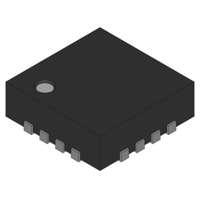
Available Package: QFN-16 (3x3 mm)
Applications
•
•
•
•
•
•
•
•
•
•
•
•
PIC®/dsPIC® Microcontroller Bias Supply
12V Industrial Input DC-DC Conversion
Set-Top Boxes
DSL Cable Modems
Automotive
Wall Cube Regulation
SLA Battery Powered Devices
AC-DC Digital Control Power Source
Power Meters
Consumer
Medical and Health Care
Distributed Power Supplies
2011-2016 Microchip Technology Inc.
High converter efficiency is achieved by integrating a
high-speed, current limited, low resistance, high-side
N-Channel MOSFET, as well as a high-speed, low
resistance, low-side N-Channel MOSFET and
associated drive circuitry. High switching frequency
minimizes the size of the inductor and output capacitor,
resulting in a small solution size.
The MCP16321/2 device can supply 1A/2A of
continuous current while regulating the output voltage
from 0.9V to 5V. A high-performance peak current
mode architecture keeps the output voltage tightly
regulated, even during input voltage steps and output
current transient conditions that are common in power
supplies.
The regulator can be turned on and off with a logic level
signal applied to the EN input. The EN input is internally
pulled up to a 4.2V reference and is rated for a
maximum of 6V. With EN low, typically 5 µA of current
is consumed from the input, making the part ideal for
power shedding and load distribution applications. The
PG output is an open-drain output pin used to interface
with other components of the system, and can be
pulled up to a maximum of 6V.
The output voltage can either be fixed at output
voltages of 0.9V, 1.5V, 1.8V, 2.5V, 3.3V, 5V or
adjustable using an external resistor divider. The
MCP16321/2 is offered in a 3x3 QFN-16 surface mount
package.
DS20002285B-page 1
�MCP16321/2
Package Type
SW
PGND
PGND
SW
MCP16321/2
3x3 QFN*
16 15 14 13
12 SW
SW 1
VIN 2
11 VIN
EP
17
VIN 3
10 BOOST
9 EN
5
6
7
8
FB
NC
NC
PG
SGND 4
* Includes Exposed Thermal Pad (EP); see Table 3-1.
Typical Applications
Typical Application with Adjustable Output Voltage
CBOOST
22 nF
L1
4.7 μH
BOOST
VIN
6.0V to 24V
SW
MCP16321/2
VIN
CIN
2x10 μF
VOUT
4.2V @ 1A/2A
EN
SGND
36.5 kȍ
VFB
COUT
2x22 μF
VOUT
10 kȍ
10 kȍ
PG
PGND
Typical Application with Fixed Output Voltage
CBOOST
22 nF
L1
4.7 μH
BOOST
VIN
6.0V to 24V
SW
MCP16321/2
VIN
CIN
2x10 μF
EN
SGND
DS20002285B-page 2
VOUT
3.3V @ 1A/2A
COUT
2x22 μF
VFB
VOUT
10 k
PG
PGND
2011-2016 Microchip Technology Inc.
�MCP16321/2
1.0
† Notice: Stresses above those listed under “Absolute
Maximum Ratings” may cause permanent damage to
the device. This is a stress rating only and functional
operation of the device at those or any other conditions
above those indicated in the operational sections of this
specification is not intended. Exposure to maximum
rating conditions for extended periods may affect
device reliability.
ELECTRICAL
CHARACTERISTICS
Absolute Maximum Ratings†
VIN .................................................................... -0.3V to 26.4V
SW ...................................................................... -1V to 26.4V
BOOST – GND ........................................... -0.3V to (VIN+6V)
EN,VFB, PG Voltage.............................................. -0.3V to 6V
Continuous Total Power Dissipation .......................................
...................................................See Thermal Characteristics
Storage Temperature ....................................-65°C to +150°C
Operating Junction Temperature...................-40°C to +125°C
ESD Protection On All Pins:
HBM ......................................................................... 3 kV
MM ..........................................................................200V
DC CHARACTERISTICS
Electrical Characteristics: Unless otherwise indicated, TA = +25°C, VIN = 12V, VOUT = 3.3V, IOUT = 300 mA,
L = 4.7 µH, COUT = 2x22 µF, CIN = 2x10 µF. Boldface specifications apply over the TJ range of -40°C to +125°C.
Parameters
Sym.
Min.
Typ.
Max.
Input Voltage
VIN
Quiescent Current
(Switching)
IQ
Quiescent Current
(Non-Switching)
Quiescent Current Shutdown
Units
Conditions
6.0
—
24
V
—
5.2
—
mA
IOUT = 0 mA
IQ
—
2.3
—
mA
Closed Loop in
Overvoltage
IOUT = 0 mA
IQ
—
5
10
µA
EN = 0
Undervoltage Lockout Start
UVLOSTRT
5.5
5.75
6.0
V
VIN Rising
Undervoltage Lockout
Hysteresis
UVLOHYS
—
0.65
—
V
Non-Switching
Maximum Output Current
MCP16321
IOUT
1
—
—
A
VIN = 6V to 24V
Maximum Output Current
MCP16322
IOUT
2
—
—
A
VIN = 6V to 24V
Output Voltage Adjust Range
VOUT
0.9
—
5.0
V
Output Voltage Tolerance
in PWM Mode
VOUT-PWM
VOUT - 2%
VOUT
VOUT + 2%
V
IOUT = 1A
Output Voltage Tolerance
in PFM Mode
VOUT-PFM
VOUT - 1% VOUT + 1% VOUT + 3.5%
V
IOUT = 0A
VIN Supply Voltage
VIN Undervoltage Lockout
Output Characteristics
Feedback Voltage
VFB
0.886
0.9
0.914
V
Feedback Reference
Tolerance
VFB-TOL
-1.5
—
1.5
%
PFM Mode Feedback
Comparator Threshold
VFB-PFM
—
VOUT + 1%
—
V
IFB
—
100
—
nA
Feedback Input Bias
Current
Note 1:
Regulator SW pin is forced off for 240 ns every eight cycles to ensure the BOOST cap is replenished.
2011-2016 Microchip Technology Inc.
DS20002285B-page 3
�MCP16321/2
DC CHARACTERISTICS (CONTINUED)
Electrical Characteristics: Unless otherwise indicated, TA = +25°C, VIN = 12V, VOUT = 3.3V, IOUT = 300 mA,
L = 4.7 µH, COUT = 2x22 µF, CIN = 2x10 µF. Boldface specifications apply over the TJ range of -40°C to +125°C.
Parameters
Sym.
Min.
Typ.
Max.
Units
VFB-PFM
—
VOUT + 1%
—
V
VIH
2.2
—
—
V
EN Input Logic Low
VIL
—
—
0.8
V
EN Input Hysteresis
VEN-HYST
—
480
—
mV
IENLK
—
3.5
—
µA
VEN = 5V
—
-1.5
—
µA
VEN = 0V
tSS
—
4
—
ms
Switching Frequency
fSW
0.9
1
1.1
Maximum Duty Cycle
DCMAX
95
97
99
PFM Mode Feedback
Conditions
EN Input Characteristics
EN Input Logic High
EN Input Leakage Current
Soft-Start Time
Switching Characteristics
Minimum Duty Cycle
MHz Open Loop VFB
Low
%
Open Loop VFB
Low
Note 1
—
7
—
%
NMOS Low-Side
Switch On Resistance
Low-Side RDS(ON)
—
120
—
m
NMOS High-Side
Switch On Resistance
High-Side
RDS(ON)
—
180
—
m
IN(MAX)
1.4
1.8
2.4
A
MCP16321
2.4
2.8
3.4
A
MCP16322
NMOS High-Side
Switch Current Limit
PG Output Characteristics
PG Low-level
Output Voltage
PGIL
—
—
0.01
V
IPG = -0.3 mA
PG High-Level Output Leakage Current
IPGLK
—
0.5
—
µA
VPG = 5V
ms
PG Release Timer
tPG
—
10
—
VOUT-UV
91% VOUT
93% VOUT
95% VOUT
VOUT Undervoltage
Hysteresis
VOUT-UV_HYST
—
1.5% VOUT
—
VOUT Overvoltage
Threshold
VOUT-OV
—
103% VOUT
—
VOUT Overvoltage
Hysteresis
VOUT-OV_HYST
—
1% VOUT
—
TSD
—
170
—
°C
TSDHYS
—
10
—
°C
VOUT Undervoltage Threshold
Thermal Characteristics
Thermal Shutdown
Die Temperature
Die Temperature
Hysteresis
Note 1:
Regulator SW pin is forced off for 240 ns every eight cycles to ensure the BOOST cap is replenished.
DS20002285B-page 4
2011-2016 Microchip Technology Inc.
�MCP16321/2
TABLE 1-1:
TEMPERATURE CHARACTERISTICS
Electrical Characteristics
Parameters
Sym.
Min.
Typ.
Max.
Units
Operating Junction Temperature
Range
TJ
-40
—
125
°C
Storage Temperature Range
TA
-65
—
150
°C
Maximum Junction Temperature
TJ
—
—
150
°C
JA
—
38.5
—
Conditions
Temperature Ranges
Steady State
Transient
Package Thermal Resistances
Thermal Resistance, 16L 3x3-QFN
Note 1:
°C/W
Note 1
2
Measured using a 4-layer FR4 Printed Circuit Board with a 13.5 in , 1 oz internal copper ground plane.
2011-2016 Microchip Technology Inc.
DS20002285B-page 5
�MCP16321/2
NOTES:
DS20002285B-page 6
2011-2016 Microchip Technology Inc.
�MCP16321/2
2.0
TYPICAL PERFORMANCE CURVES
The graphs and tables provided following this note are a statistical summary based on a limited number of
samples and are provided for informational purposes only. The performance characteristics listed herein
are not tested or guaranteed. In some graphs or tables, the data presented may be outside the specified
operating range (e.g., outside specified power supply range) and therefore outside the warranted range.
Note:
100
95
90
85
80
75
70
65
60
55
50
100
VIN = 6V
VIN = 12V
VIN = 18V
VIN = 24V
VOUT = 5V
0.8
1.2
IOUT (A)
1.6
VOUT = 1.8V
5V VOUT Efficiency vs. IOUT.
0
VIN = 6V
80
VIN = 12V
75
VIN = 18V
70
VOUT = 3.3V
65
60
VIN = 24V
55
50
0
0.4
0.8
1.2
IOUT (A)
1.6
90
85
80
75
70
65
60
55
50
45
40
0.8
1.2
IOUT (A)
1.6
2
1.8V VOUT Efficiency vs.
VIN = 6V
VIN = 12V
VIN = 18V
VOUT = 1.5V
0
2
3.3V VOUT Efficiency vs.
FIGURE 2-2:
IOUT.
0.4
FIGURE 2-4:
IOUT.
Efficiency (%)
Efficiency (%)
VIN = 18V
60
2.0
85
0.4
0.8
1.2
IOUT (A)
1.6
2
1.5V VOUT Efficiency vs.
FIGURE 2-5:
IOUT.
100
100
VIN = 6V
90
Efficiency (%)
90
Efficiency (%)
VIN = 12V
70
40
0.4
FIGURE 2-1:
90
80
50
0.0
95
VIN = 6V
90
Efficiency (%)
Efficiency (%)
Note: Unless otherwise indicated, VIN = 12V, EN = Floating (Internally pulled up), CIN = 20 µF, COUT = 2x22 µF,
L = 4.7 µH (XAL6060-472MEB), ILOAD = 200 mA, TA = +25°C. MCP16321 maximum output current = 1A.
80
VIN = 12V
70
VIN = 18V
60
VIN = 6V
80
70
VIN = 8V
60
VOUT = 0.9V
VOUT = 2.5V
50
VIN = 24V
50
40
VIN = 10V
40
0
FIGURE 2-3:
IOUT.
0.4
0.8
1.2
IOUT (A)
1.6
2
2.5V VOUT Efficiency vs.
2011-2016 Microchip Technology Inc.
0
FIGURE 2-6:
IOUT.
0.4
0.8
1.2
IOUT (A)
1.6
2
0.9V VOUT Efficiency vs.
DS20002285B-page 7
�MCP16321/2
Note: Unless otherwise indicated, VIN = 12V, EN = Floating (Internally pulled up), CIN = 20 µF, COUT = 2x22 µF,
L = 4.7 µH (XAL6060-472MEB), ILOAD = 200 mA, TA = +25°C. MCP16321 maximum output current = 1A.
5.04
VOUT = 5V
5.03
VOUT (V)
5.01
VOUT (V)
VIN = 6V
5.02
VIN = 12V
5
VIN = 18V
VIN = 24V
4.99
4.98
0
0.4
FIGURE 2-7:
0.8
1.2
IOUT (A)
1.6
1.808
1.807
1.806
1.805
1.804
1.803
1.802
1.801
1.8
1.799
1.798
2
5V VOUT vs. IOUT.
VOUT =1.8V
VIN = 6V
VIN = 12V
VIN = 18V
0
0.4
FIGURE 2-10:
3.32
0.8
1.2
IOUT (A)
1.6
2
1.8V VOUT vs. IOUT.
1.505
VOUT =3.3V
VOUT =1.5V
1.504
3.315
VIN = 6V
3.305
VOUT (V)
VOUT (V)
1.503
3.31
VIN = 12V
VIN = 6V
1.502
1.501
VIN = 12V
1.5
3.3
VIN = 24V
3.295
0
0.4
1.498
1.6
2
3.3V VOUT vs. IOUT.
2.515
2.513
2.511
2.509
2.507
2.505
2.503
2.501
2.499
2.497
2.495
0
0.4
FIGURE 2-11:
0.8
1.2
IOUT (A)
1.6
2
1.5V VOUT vs. IOUT.
0.904
VOUT =0.9V
VOUT =2.5V
0.903
0.902
VIN = 6V
VOUT (V)
VOUT (V)
FIGURE 2-8:
0.8
1.2
IOUT (A)
VIN = 16V
1.499
VIN = 18V
VIN = 12V
VIN = 6V
0.901
0.9
VIN = 8V
0.899
VIN = 10V
VIN = 24V
0.898
VIN = 18V
0.897
0
0.4
FIGURE 2-9:
DS20002285B-page 8
0.8
1.2
IOUT (A)
1.6
2.5V VOUT vs. IOUT.
2
0
FIGURE 2-12:
0.4
0.8
1.2
IOUT (A)
1.6
2
0.9V VOUT vs. IOUT.
2011-2016 Microchip Technology Inc.
�MCP16321/2
Note: Unless otherwise indicated, VIN = 12V, EN = Floating (Internally pulled up), CIN = 20 µF, COUT = 2x22 µF,
L = 4.7 µH (XAL6060-472MEB), ILOAD = 200 mA, TA = +25°C. MCP16321 maximum output current = 1A.
5.02
1.804
VOUT = 1.8V
VOUT = 5V
5.015
1.803
1.802
VOUT (V)
VOUT (V)
5.01
5.005
1.801
IOUT = 1A
5
1.8
4.995
IOUT = 2A
4.99
IOUT = 1A
1.799
IOUT = 2A
1.798
4.985
6
8
10
FIGURE 2-13:
12
14 16
VIN (V)
18
20
22
6
24
5V VOUT vs VIN.
12
VIN (V)
14
16
18
1.8V VOUT vs VIN.
1.503
VOUT = 3.3V
3.308
VOUT = 1.5V
1.5025
1.502
3.306
IOUT = 2A
1.5015
3.304
VIN (V)
VOUT (V)
10
FIGURE 2-16:
3.31
3.302
IOUT = 1A
3.3
1.501
1.5005
1.5
3.298
IOUT = 1A
1.4995
3.296
1.499
IOUT = 2A
1.4985
3.294
6
8
10
FIGURE 2-14:
12
14 16
VIN (V)
18
20
22
3.3V VOUT vs VIN.
2.506
2.505
2.504
2.503
2.502
2.501
2.5
2.499
2.498
2.497
2.496
6
24
8
10
12
VOUT (V)
FIGURE 2-17:
14
16
1.5V VOUT vs VIN.
0.9012
VOUT = 2.5V
VOUT = 0.9V
0.901
0.9008
VOUT (V)
VOUT (V)
8
IOUT = 1A
0.9006
0.9004
0.9002
IOUT = 1A
0.9
0.8998
IOUT = 2A
0.8996
IOUT = 2A
0.8994
6
8
FIGURE 2-15:
10
12
14 16
VIN (V)
18
20
2.5V VOUT vs VIN.
2011-2016 Microchip Technology Inc.
22
24
6
FIGURE 2-18:
7
8
VIN (V)
9
10
0.9V VOUT vs VIN.
DS20002285B-page 9
�MCP16321/2
Note: Unless otherwise indicated, VIN = 12V, EN = Floating (Internally pulled up), CIN = 20 µF, COUT = 2x22 µF,
L = 4.7 µH (XAL6060-472MEB), ILOAD = 200 mA, TA = +25°C. MCP16321 maximum output current = 1A.
1020
Oscillator Frequency (kHz)
Shudown Current (µA)
8
7
6
5
4
3
2
1
0
10
14
VIN (V)
18
1005
1000
995
990
985
22
Shutdown Current vs. Input
-40
4.90
4.85
4.80
4.75
4.70
4.65
4.60
4.55
4.50
4.45
-40
-10
20
50
80
Ambient Temperature (°C)
FIGURE 2-20:
Temperature.
IOUT = 0.1A
3.298
3.296
IOUT = 1A
3.294
3.292
3.290
3.288
3.286
3.284
-40
-10
20
50
80
Ambient Temperature (°C)
FIGURE 2-21:
Temperature.
DS20002285B-page 10
Output Voltage vs.
110
110
5.45
IOUT = 0A
5.40
5.35
5.30
5.25
5.20
-40
-10
20
50
80
Ambient Temperature (°C)
110
FIGURE 2-23:
Input Quiescent Current vs.
Temperature (No Load, Switching).
Non-Switching Quiscent Current
(mA)
3.300
20
50
80
Ambient Temperature (°C)
5.50
110
Shutdown Current vs.
-10
FIGURE 2-22:
Oscillator Frequency vs.
Temperature (IOUT = 300 mA).
Switching Quiscent Current (mA)
FIGURE 2-19:
Voltage.
Shutdown Current (µA)
1010
980
6
VOUT (V)
1015
2.42
2.40
IOUT = 0A
2.38
2.36
2.34
2.32
2.30
2.28
-40
-10
20
50
80
Ambient Temperature (°C)
110
FIGURE 2-24:
Input Current vs.
Temperature (No Load, No Switching).
2011-2016 Microchip Technology Inc.
�MCP16321/2
Note: Unless otherwise indicated, VIN = 12V, EN = Floating (Internally pulled up), CIN = 20 µF, COUT = 2x22 µF,
L = 4.7 µH (XAL6060-472MEB), ILOAD = 200 mA, TA = +25°C. MCP16321 maximum output current = 1A.
VOUT = 3.3V
IOUT = 200 mA
VIN = 12V
30
Typical Mininimum Duty Cycle = 7%
Max VIN (V)
25
20
15
10
5
0
0.9
1.2
1.5
VOUT (V)
1.8
2.1
FIGURE 2-25:
Maximum VIN to VOUT Ratio
for Continuous Switching.
VOUT = 3.3V
IOUT = 50 mA
VIN = 12V
FIGURE 2-26:
Waveforms.
Start-up From Enable.
VOUT = 3.3V
IOUT = 200 mA
VIN = 12V
Light Load Switching
FIGURE 2-29:
Start-up From VIN.
VOUT = 3.3V
IOUT = 100 mA to 600 mA
VIN = 12V
VOUT = 3.3V
IOUT = 500 mA
VIN = 12V
FIGURE 2-27:
Waveforms.
FIGURE 2-28:
Heavy Load Switching
2011-2016 Microchip Technology Inc.
FIGURE 2-30:
Load Transient Response.
DS20002285B-page 11
�MCP16321/2
Note: Unless otherwise indicated, VIN = 12V, EN = Floating (Internally pulled up), CIN = 20 µF, COUT = 2x22 µF,
L = 4.7 µH (XAL6060-472MEB), ILOAD = 200 mA, TA = +25°C. MCP16321 maximum output current = 1A.
VOUT = 3.3V
IOUT = 200 mA
VIN = 6V to 10V
FIGURE 2-31:
DS20002285B-page 12
Line Transient Response.
2011-2016 Microchip Technology Inc.
�MCP16321/2
3.0
PIN DESCRIPTIONS
The descriptions of the pins are listed in Table 3-1.
TABLE 3-1:
PIN FUNCTION TABLE
MCP16321/2
3x3 QFN
Symbol
1
SW
Output switch node, connects to the inductor and the bootstrap capacitor
2
VIN
Input supply voltage pin for power and internal biasing
3.1
Description
3
VIN
4
SGND
5
VFB
Output voltage feedback pin. Connect VFB to VOUT for fixed version and output
resistor divider for adjustable version.
6
NC
No Connection
7
NC
No Connection
8
PG
Power Good open-drain output, pulled up to a maximum of 6V
9
EN
Enable input pin. Logic high enables the operation. Internally pulled up, pull EN pin
low to disable regulator’s output. Maximum voltage on EN input is 6V.
10
BOOST
Boost voltage that drives the internal NMOS control switch. A bootstrap capacitor
is connected between the BOOST and SW pins.
11
VIN
Input supply voltage pin for power and internal biasing
12
SW
Output switch node, connects to the inductor and the bootstrap capacitor
13
SW
Output switch node, connects to the inductor and the bootstrap capacitor
14
PGND
GND supply for the internal low-side NMOS/integrated diode
15
PGND
GND supply for the internal low-side NMOS/integrated diode
16
SW
Output switch node, connects to the inductor and the bootstrap capacitor
17
EP
Exposed Thermal Pad (EP); must be connected to GND
Input supply voltage pin for power and internal biasing
Primary signal ground
Switch Pin (SW)
The drain of the low-side N-Channel switch is
connected internally to the source of the high-side
N-Channel switch, and externally to the SW node,
consisting of the inductor and bootstrap capacitor. The
SW node can rise very fast as a result of the internal
high-side switch turning on. It should be connected
directly to the 4.7 µH inductor with a wide, short trace.
3.2
Power Supply Input Voltage Pin
(VIN)
Connect the input voltage source to VIN. The input
source should be decoupled to GND using 2 x 10 µF
capacitors. The amount of the capacitance depends on
the impedance of the source and output current. The
input capacitors provide AC current for the high-side
power switch and a stable voltage source for the
internal device power. This capacitor should be
connected as close as possible to the VIN and GND
pins.
2011-2016 Microchip Technology Inc.
3.3
Signal Ground Pin (SGND)
This ground is used for the majority of the device,
including the analog reference, control loop, and other
circuits.
3.4
Feedback Voltage Pin (VFB)
The VFB input pin is used to provide output voltage
regulation by either using a resistor divider or VOUT
directly. For the adjustable version, the VFB will be 0.9V
typical with the output voltage in regulation. For the
fixed version, the VFB will be equal to the
corresponding VOUT value.
3.5
Power Good Pin (PG)
PG is an open-drain, active-low output. The regulator
output voltage is monitored and the PG line will remain
low until the output voltage reaches the VOUT-UV
threshold. Once the internal comparator detects that
the output voltage is above the VOUT-UV threshold, an
internal delay timer is activated. After a 10 ms delay,
the PG open-drain output pin can be pulled high,
indicating that the output voltage is in regulation. The
maximum voltage applied to the PG output pin should
not exceed 6V.
DS20002285B-page 13
�MCP16321/2
3.6
Enable Pin (EN)
The EN input pin is a logic-level input used to enable or
disable the device. A logic high (> 2.2V) will enable the
regulator output, while a logic low (< 0.8V) will ensure
that the regulator is disabled. This pin is internally
pulled up to an internal reference and will be enabled
when VIN > UVLO, unless the EN pin is pulled low. The
maximum input voltage applied to the EN pin should
not exceed 6V.
3.7
BOOST Pin (BOOST)
This pin will provide the bootstrap voltage required for
driving the upper internal NMOS switch of the buck
regulator. An external ceramic capacitor placed
between the BOOST input pin and the SW pin will
provide the necessary drive voltage for the upper
switch. During steady state operation, the capacitor is
recharged on every low-side, synchronous switching
cycle. If the Switch mode approaches 100% duty cycle
for the high-side MOSFET, the device will automatically
reduce the duty cycle switch to a minimum off time of
240 ns on every 8th cycle to recharge the boost
capacitor.
3.8
Power Ground Pin (PGND)
This is a separate ground connection used for the lowside synchronous switch to isolate switching noise from
the rest of the device.
3.9
Exposed Thermal Pad (EP)
There is no internal electrical connection between the
Exposed Thermal Pad (EP) and the PGND and SGND
pins. The EP must be connected to GND on the Printed
Circuit Board (PCB).
DS20002285B-page 14
2011-2016 Microchip Technology Inc.
�MCP16321/2
4.0
DETAILED DESCRIPTION
4.1
Device Overview
The MCP16321/2 is a high-input voltage, step-down
regulator, capable of supplying 1A/2A to a regulated
output voltage from 0.9V to 5V. Internally, the 1 MHz
oscillator provides a fixed frequency, while the Peak
Current Mode Control architecture varies the duty cycle
for output voltage regulation. An internal floating driver
is used to turn the high-side integrated N-Channel
MOSFET on and off. The power for this driver is
derived from an external boost capacitor whose energy
is replenished when the low-side N-Channel MOSFET
is turned on. When the maximum duty cycle
approaches 100%, the boost capacitor is replenished
for 240 ns after every eight cycles.
4.1.1
INTERNAL REFERENCE VOLTAGE
VREF
For the adjustable version, an integrated precise 0.9V
reference combined with an external resistor divider
sets the desired converter output voltage. The resistor
divider can vary without affecting the control system
gain. High-value resistors consume less current, but
are more susceptible to noise. For the fixed version, an
integrated precise voltage reference is set to the
desired VOUT value and is directly connected to VOUT.
4.1.2
INTERNAL COMPENSATION
All control system components necessary for stable
operation over the entire device operating range are
integrated, including the error amplifier and inductor
current slope compensation.
4.1.3
EXTERNAL COMPONENTS
External components consist of:
•
•
•
•
Input capacitor
Output filter (inductor and capacitor)
Boost capacitor
Resistor divider (adjustable version only)
The selection of the external inductor, output capacitor,
input capacitor and boost capacitor is dependent upon
the output voltage and the maximum output current.
2011-2016 Microchip Technology Inc.
4.1.4
ENABLE INPUT
The enable input (EN) is used to disable the device. If
disabled, the device consumes a minimal current from
the input. Once enabled, the internal soft start controls
the output voltage rate of rise, preventing high-inrush
current and output voltage overshoot. The EN is
internally pulled up or enabled; to disable the converter,
it must be pulled low.
4.1.5
SOFT START
The internal reference voltage rate of rise is controlled
during start-up, minimizing the output voltage overshoot and the inrush current.
4.1.6
OUTPUT OVER VOLTAGE
PROTECTION
If the output of the regulator exceeds 103% of the
regulation voltage, the SW outputs will tri-state to
protect the device from damage. This check occurs at
the start of each switching cycle.
4.1.7
INPUT UNDERVOLTAGE LOCKOUT
An integrated Undervoltage Lockout (UVLO) prevents
the converter from starting until the input voltage is high
enough for normal operation. The converter will
typically start at 5.75V (typical) and operate down to
5.25V (typical). Hysteresis of 500 mV (typical) is added
to prevent starting and stopping during start-up, as a
result of loading the input voltage source.
4.1.8
MINIMUM DUTY CYCLE
A minimum duty cycle of 70 ns typical prevents the
device from constant switching for high step-down
voltage ratios. Duty cycles less than this minimum will
initiate pulse skipping to maintain output voltage
regulation, resulting in higher output voltage ripple.
Duty cycle for continuous inductor current operation is
approximated by VOUT/VIN. For a 1 MHz switching
frequency or 1 µs period, this results in a 7% duty cycle
minimum. Maximum VIN for continuous switching can
be approximated dividing VOUT by the minimum duty
cycle or 7%. For example, the maximum input voltage
for continuous switching for a 1.5V output is equal to
approximately 21V.
DS20002285B-page 15
�MCP16321/2
4.1.9
OVERTEMPERATURE
PROTECTION
Overtemperature protection limits the silicon die
temperature to +170°C by turning the converter off. The
normal switching resumes at +160°C.
VIN
CIN
UV
Protection
VOUT
OTEMP
Protection
EN
Monitor and
Control
4.2V
PG
BOOST
Voltage
Current
Limit
VOUT
RTOP
Slope
Comp
OV
Protection
FB
BOOST
+
RBOT
CS
+
CBOOST
VREF and
Softstart
+
+
COMP
-
PWM
Comparator
Amp
HS
Drive
-
Compensation
1 MHz
Oscillator
Gate Drive
Control
L
VOUT
Internal Bias
LS
Drive
-
VREF
SW
COUT
COMP
+
PFM
Comparator
SGND
FIGURE 4-1:
DS20002285B-page 16
PGND
MCP16321/2 Block Diagram.
2011-2016 Microchip Technology Inc.
�MCP16321/2
4.2
Functional Description
L
4.2.1
STEP-DOWN OR BUCK
CONVERTER
IL
The MCP16321/2 is a synchronous, step-down or buck
converter capable of stepping input voltages ranging
from 6V to 24V down to 0.9V to 5V.
The integrated high-side switch is used to chop or
modulate the input voltage using a controlled duty cycle
for output voltage regulation. The integrated low-side
switch is used to freewheel current when the high-side
switch is turned off. High efficiency is achieved by using
low-resistance switches and low equivalent series
resistance (ESR), inductor and capacitors. When the
high-side switch is turned on, a DC voltage is applied to
the inductor (VIN – VOUT), resulting in a positive linear
ramp of inductor current. When the high-side switch
turns off and the low-side switch turns on, the applied
inductor voltage is equal to –VOUT, resulting in a
negative linear ramp of inductor current. In order to
ensure there is no shoot-through current, a dead time
where both switches are off is implemented between
the high-side switch turning off and the low-side switch
turning on, and the low-side switch turning off and the
high-side switch turning on.
For steady-state, continuous inductor current
operation, the positive inductor current ramp must
equal the negative current ramp in magnitude. While
operating in steady state, the switch duty cycle must be
equal to the relationship of VOUT/VIN for constant
output voltage regulation, under the condition that the
inductor current is continuous, or never reaches zero.
For discontinuous inductor current operation, the
steady-state duty cycle will be less than VOUT/VIN to
maintain voltage regulation. When the inductor current
reaches zero, the low-side switch is turned off so that
current does not flow in the reverse direction, keeping
the efficiency high. The average of the chopped input
voltage or SW node voltage is equal to the output
voltage, while the average inductor current is equal to
the output current.
2011-2016 Microchip Technology Inc.
VOUT
S1
COUT
VIN
S2
IL
IOUT
VIN
SW
VOUT
S1 ON
S2 ON
Continuous Inductor Current Mode
IL
IOUT
VIN
SW
S1 ON S2 Both
ON OFF
Discontinuous Inductor Current Mode
FIGURE 4-2:
Converter.
Synchronous Step-Down
DS20002285B-page 17
�MCP16321/2
4.2.2
PEAK CURRENT MODE CONTROL
The MCP16321/2 integrates a Peak Current Mode
Control architecture, resulting in superior AC regulation
while minimizing the number of voltage loop
compensation components, and their size, for
integration. Peak Current Mode Control takes a small
portion of the inductor current, replicates it and
compares this replicated current sense signal with the
output of the integrated error voltage. In practice, the
inductor current and the internal switch current are
equal during the switch-on time. By adding this peak
current sense to the system control, the step-down
power train system can be approximated by a 1st order
system rather than a 2nd order system. This reduces
the system complexity and increases its dynamic
performance.
For Pulse-Width Modulation (PWM) duty cycles that
exceed 50%, the control system can become bimodal,
where a wide pulse followed by a short pulse repeats
instead of the desired fixed pulse width. To prevent this
mode of operation, an internal compensating ramp is
summed into the current sense signal.
4.2.3
PULSE WIDTH MODULATION
(PWM)
The internal oscillator periodically starts the switching
period, which in the MCP16321/2’s case occurs every
1 µs or 1 MHz. With the high-side integrated
N-Channel MOSFET turned on, the inductor current
ramps up until the sum of the current sense and slope
compensation ramp exceeds the integrated error
amplifier output. Once this occurs, the high-side switch
turns off and the low-side switch turns on. The error
amplifier output slews up or down to increase or
decrease the inductor peak current feeding into the
output LC filter. If the regulated output voltage is lower
than its target, the inverting error amplifier output rises.
This results in an increase in the inductor current to
correct for errors in the output voltage. The fixed
frequency duty cycle is terminated when the sensed
inductor peak current, summed with the internal slope
compensation, exceeds the output voltage of the error
amplifier. The PWM latch is set by turning off the highside internal switch and preventing it from turning on
until the beginning of the next cycle.
DS20002285B-page 18
4.2.4
HIGH-SIDE DRIVE
The MCP16321/2 features an integrated high-side
N-Channel MOSFET for high efficiency step-down
power conversion. An N-Channel MOSFET is used for
its low resistance and size (instead of a P-Channel
MOSFET). The N-Channel MOSFET gate must be
driven above its source to fully turn on the device,
resulting in a gate-drive voltage above the input to turn
on the high-side N-Channel. The high-side N-Channel
source is connected to the inductor and boost cap or
switch node. When the high-side switch is off and the
low-side is on, the inductor current flows through the
low-side switch, providing a path to recharge the boost
cap from the boost voltage source. An internal boostblocking diode is used to prevent current flow from the
boost cap back into the output during the internal
switch-on time. Prior to start-up, the boost cap has no
stored charge to drive the switch. An internal regulator
is used to “pre-charge” the boost cap. Once precharged, the switch is turned on and the inductor
current flows. When the high-side switch turns off and
the low-side turns on, current freewheels through the
inductor and low-side switch, providing a path to
recharge the boost cap. When the duty cycle
approaches its maximum value, there is very little time
for the boost cap to be recharged due to the short
amount time that the low-side switch is on. Therefore,
when the maximum duty cycle approaches, the switch
node is forced off for 240 ns every eight cycles to
ensure that the boost cap gets replenished.
2011-2016 Microchip Technology Inc.
�MCP16321/2
5.0
APPLICATION INFORMATION
5.0.1
TYPICAL APPLICATIONS
The MCP16321/2 synchronous step-down converter
operates over a wide input range, up to 24V maximum.
Typical applications include generating a bias or VDD
voltage for PIC® microcontrollers, digital control system
bias supply for AC-DC converters and 12V industrial
input and similar applications.
5.0.2
ADJUSTABLE OUTPUT VOLTAGE
CALCULATIONS
5.0.3
The step-down converter duty cycle can be estimated
using Equation 5-2 while operating in Continuous
Inductor Current Mode. This equation accounts for the
forward drop of two internal N-Channel MOSFETS. As
load current increases, the voltage drop in both internal
switches will increase, requiring a larger PWM duty
cycle to maintain the output voltage regulation. Switch
voltage drop is estimated by multiplying the switch
current times the switch resistance or RDSON.
EQUATION 5-2:
To calculate the resistor divider values for the
MCP16321/2 adjustable version, use Equation 5-1.
RTOP is connected to VOUT, RBOT is connected to
SGND, and both are connected to the VFB input pin.
EQUATION 5-1:
RESISTOR DIVIDER
CALCULATION
R TOP
V OUT = V FB 1 + ------------
R BOT
EXAMPLE 5-1:
2.0V RESISTOR DIVIDER
VOUT = 2.0V
VFB = 0.9V
RBOT = 10 k
RTOP = 12.2 k (standard value = 12.3 k)
VOUT = 2.007V (using standard values)
EXAMPLE 5-2:
4.2V RESISTOR DIVIDER
VOUT = 4.2V
VFB = 0.9V
RBOT = 10 k
RTOP = 36.7 k (standard value = 36.5 k)
VOUT = 4.185V (using standard values)
The error amplifier is internally compensated to ensure
loop stability. External resistor dividers, inductance and
output capacitance, all have an impact on the control
system and should be selected carefully and evaluated
for stability. A 10 kΩ resistor is recommended as a
good trade-off for quiescent current and noise
immunity.
GENERAL DESIGN EQUATIONS
CONTINUOUS INDUCTOR
CURRENT DUTY CYCLE
V OUT + I LSW R DSONL
D = ------------------------------------------------------------V IN – I HSW R DSONH
5.0.4
INPUT CAPACITOR SELECTION
The step-down converter input capacitor must filter the
high-input ripple current, as a result of pulsing or
chopping the input voltage. The MCP16321/2 input
voltage pin is used to supply voltage for the power train
and as a source for internal bias. A low equivalent
series resistance (ESR), preferably a ceramic
capacitor,
is
recommended.
The
necessary
capacitance is dependent upon the maximum load
current and source impedance. Three capacitor
parameters to keep in mind are the voltage rating,
equivalent series resistance and the temperature
rating. For wide temperature range applications, a
multilayer X7R dielectric is recommended, while for
applications with limited temperature range, a
multilayer X5R dielectric is acceptable. The input
capacitor voltage rating must be VIN plus margin.
5.0.5
OUTPUT CAPACITOR SELECTION
The output capacitor provides a stable output voltage
during sudden load transients, and reduces the output
voltage ripple. As with the input capacitor, X5R and
X7R ceramic capacitors are well suited for this application.
The MCP16321/2 is internally compensated, so the
output capacitance range is limited. See TABLE 5-1:
“Capacitor Value Range” for the recommended output capacitor range.
The amount and type of output capacitance and
equivalent series resistance will have a significant
effect on the output ripple voltage and system stability.
The range of the output capacitance is limited due to
the integrated compensation of the MCP16321/2.
The output voltage capacitor rating should be a
minimum of VOUT plus margin.
TABLE 5-1:
2011-2016 Microchip Technology Inc.
CAPACITOR VALUE RANGE
Parameter
Min
Max
CIN
8 µF
None
DS20002285B-page 19
�MCP16321/2
TABLE 5-1:
CAPACITOR VALUE RANGE
Parameter
Min
Max
COUT
33 µF
None
5.0.6
INDUCTOR SELECTION
The MCP16321/2 is designed to be used with small
surface mount inductors. Several specifications should
be considered prior to selecting an inductor. To
optimize system performance, low ESR inductors
should be used.
EQUATION 5-3:
INDUCTOR CURRENT
RIPPLE
V
I L = -----L- t ON
L
TABLE 5-2:
MCP16321 RECOMMENDED
INDUCTORS
Value
(µH)
DCR
()
ISAT
(A)
Size
WxLxH
(mm)
1008PS
4.7
0.35
1.7
3.81x3.78x2.74
LPS4012
4.7
0.175
1.8
4.1x4.1x1.2
LPS4018
4.7
0.125
1.9
4.1x4.1x1.8
LPS5015
4.7
0.15
1.8
5x5x1.5
MSS5121
4.7
0.095
1.66
5.1x5.1x2.2
LPS5030
4.7
0.083
2
5x5x3
MSS6122
4.7
0.065
1.82
6.1x6.1x2.2
MOS6020
4.7
0.05
1.94
6.8x6x2.4
Part
Number
Coilcraft®
Wurth Elektronik®
EXAMPLE 5-3:
MCP16321 PEAK
INDUCTOR CURRENT – 1A
VIN = 12V
744042
4.7
0.07
1.65
4.8x4.8x1.8
744068
4.7
0.072
1.55
8x8x1.1
7448944
4.7
0.0545
4.2
8x8x3.8
LTF5022T
4.7
0.073
2
5.2x5x2.2
VLC5020T
4.7
0.097
2
5x5x2
EPCOS®
VOUT = 3.3V
IOUT = 1A
L = 4.7 µH
IL
I LPK = --------- + IOUT
2
Inductor ripple current = 509 mA
VLC6020T
4.7
0.079
1.8
6x6x2
VLCF5020T
4.7
0.122
1.7
5x5x2
VLF5014ST
4.7
0.12
1.7
4.8x4.6x1.4
TABLE 5-3:
Inductor peak current = 1.255A
An inductor saturation rating minimum of 1.255A is
recommended. A trade-off between size, cost and
efficiency is made to achieve the desired results.
EXAMPLE 5-4:
MCP16322 PEAK
INDUCTOR CURRENT – 2A
MCP16322 RECOMMENDED
INDUCTORS
Value
(µH)
DCR
()
ISAT
(A)
Size
WxLxH
(mm)
MSS6132-472
4.7
0.056
2.84
6.1x6.1x3.2
Part Number
Coilcraft®
LPS6225-472
4.7
0.065
3.2
6.2x6.2x2.5
VIN = 12V
MSS7341-502
4.7
0.024
3.16
7.3x7.3x4.1
VOUT = 3.3V
DO1813H-472
4.7
0.054
2.6
8.89x6.1x5.0
IOUT = 2A
Wurth Elektronik®
L = 4.7 µH
7447785004
4.7
0.06
2.5
5.9x6.2x3.3
IL
I LPK = --------- + IOUT
2
7447786004
4.7
0.057
2.8
5.9x6.2x5.1
7447789004
4.7
0.033
3.9
7.3x3.2x1.5
EPCOS
®
Inductor ripple current = 509 mA
B82464G2
4.7
0.033
3.1
10.4x10.4x3.0
Inductor peak current = 2.255A
B82464A2
4.7
0.03
4.5
10.4x10.4x3.0
An inductor saturation rating minimum of 2.255A is
recommended. A trade-off between size, cost and
efficiency is made to achieve the desired results.
DS20002285B-page 20
2011-2016 Microchip Technology Inc.
�MCP16321/2
5.0.7
BOOST CAPACITOR
The boost capacitor is used to supply current for the
internal high-side drive circuitry that is above the input
voltage. The boost capacitor must store enough energy
to completely drive the high-side switch on and off. A
22 nF X5R or X7R capacitor is recommended for all
applications. The boost capacitor maximum voltage is
5.5V, so a 6.3V or 10V rated capacitor is
recommended.
5.0.8
EXAMPLE 5-5:
To quickly estimate the internal power dissipation for
the switching step-down regulator, an empirical
calculation using measured efficiency can be used.
Given the measured efficiency, the internal power
dissipation is estimated in Equation 5-4. This power
dissipation includes all internal and external
component losses. For a quick internal estimate,
subtract the estimated inductor ESR loss from the PDIS
calculation in Equation 5-4.
EQUATION 5-4:
TOTAL POWER
DISSIPATION ESTIMATE
V OUT I OUT
PDIS = ------------------------------- – VOUT I OUT
Efficency
The difference between the first term, input power, and
the second term, power delivered, is the total system
power dissipation. The inductor losses are estimated
by PL = IOUT2 x LESR.
VIN =
12V
VOUT =
IOUT =
5.0V
Efficiency
=
92.5%
=
405 mW
LESR =
0.04
PL =
40 mW
MCP16321 internal power dissipation estimate:
PDIS – PL =
JA =
Estimated Junction
=
365 mW
38.5°C/W
+14.052°C
Note 1: JA = 38.5°C/W for a 4-layer FR4 Printed
Circuit Board with a 13.5 in2, 1 oz internal
copper ground plane.
2: A smaller ground plane will result in a
larger JA temperature rise.
EXAMPLE 5-6:
POWER DISSIPATION –
MCP16322
VIN =
12V
VOUT =
3.3V
IOUT =
2A
Efficiency
=
87.5%
Total System Dissipation
=
943 mW
LESR =
PL =
0.04
160 mW
MCP16322 internal power dissipation estimate:
PDIS – PL =
JA =
Estimated Junction
2011-2016 Microchip Technology Inc.
1A
Total System Dissipation
THERMAL CALCULATIONS
The MCP16321/2 is available in a 3x3 QFN-16
package. By calculating the power dissipation and
applying the package thermal resistance (θJA), the
junction temperature is estimated. The maximum
continuous junction temperature rating for the
MCP16321/2 is +125°C.
POWER DISSIPATION –
MCP16321
=
783 mW
38.5°C/W
+30.14°C
DS20002285B-page 21
�MCP16321/2
5.0.9
PCB LAYOUT INFORMATION
frequency switch current, CIN also provides a stable
voltage source for the internal MCP16321/2 circuitry.
Unstable PWM operation can result if there are
excessive transients or ringing on the VIN pin of the
MCP16321/2 device. In Figure 5-1, CIN is placed close
to the VIN pins. A ground plane on the bottom of the
board provides a low resistive and low inductive path
for the return current. The next priority in placement is
the freewheeling current loop formed by COUT and L
while strategically placing the COUT return close to CIN
return. Next, CBOOST should be placed between the
boost pin and the switch node pin. This leaves space
close to the MCP16321/2 VFB pin to place RTOP and
RBOT. RTOP and RBOT are routed away from the switch
node so noise is not coupled into the high-impedance
VFB input.
Good printed circuit board layout techniques are
important to any switching circuitry, and switching
power supplies are no different. When wiring the
switching high-current paths, short and wide traces
should be used. Therefore, it is important that the input
and output capacitors be placed as close as possible to
the MCP16321/2 to minimize the loop area.
The feedback resistors and feedback signal should be
routed away from the switching node and the switching
current loop. When possible, ground planes and traces
should be used to help shield the feedback signal and
minimize noise and magnetic interference.
A good MCP16321/2 layout starts with CIN placement.
CIN supplies current to the input of the circuit when the
switch is turned on. In addition to supplying high-
Bottom layer is ground plane
VOUT
COUT
L
COUT
RPG 10Ω
CBOOST
GND
MCP16321/2
RBOT RTOP
Trace on
bottom layer
CIN
VIN
FIGURE 5-1:
DS20002285B-page 22
CIN
GND
Recommended Layout.
2011-2016 Microchip Technology Inc.
�MCP16321/2
CBOOST
VOUT
0.9V to 5V
L
BOOST
VIN
6.0V to 24V
SW
VIN
MCP16321/2
10Ω
EN
CIN
RTOP
COUT
VFB
VOUT
RBOT
RPG
PG
SGND
FIGURE 5-2:
TABLE 5-4:
PGND
Recommended Layout – Schematic.
RECOMMENDED LAYOUT
COMPONENTS
Component
Value
CIN
2 x 10 µF
COUT
2 x 22 µF
L
4.7 µH
RTOP
36.5 k
RBOT
10 k
RPG
10 k
CBOOST
22 nF
2011-2016 Microchip Technology Inc.
DS20002285B-page 23
�MCP16321/2
NOTES:
DS20002285B-page 24
2011-2016 Microchip Technology Inc.
�MCP16321/2
6.0
PACKAGING INFORMATION
6.1
Package Marking Information
16-Lead QFN (3x3x0.9 mm)
Example
Part Number
Legend: XX...X
Y
YY
WW
NNN
e3
*
Note:
Code
MCP16321T-150E/NG
AAA
MCP16321T-180E/NG
AAB
MCP16321T-250E/NG
AAC
MCP16321T-330E/NG
AAD
MCP16321T-500E/NG
AAE
MCP16321T-ADJE/NG
AAF
MCP16322T-150E/NG
ABA
MCP16322T-180E/NG
ABB
MCP16322T-250E/NG
ABC
MCP16322T-330E/NG
ABD
MCP16322T-500E/NG
ABE
MCP16322T-ADJE/NG
ABF
AAA
E114
5256
Customer-specific information
Year code (last digit of calendar year)
Year code (last 2 digits of calendar year)
Week code (week of January 1 is week ‘01’)
Alphanumeric traceability code
Pb-free JEDEC designator for Matte Tin (Sn)
This package is Pb-free. The Pb-free JEDEC designator ( e3 )
can be found on the outer packaging for this package.
In the event the full Microchip part number cannot be marked on one line, it will
be carried over to the next line, thus limiting the number of available
characters for customer-specific information.
2011-2016 Microchip Technology Inc.
DS20002285B-page 25
�MCP16321/2
DS20002285B-page 26
2011-2016 Microchip Technology Inc.
�MCP16321/2
2011-2016 Microchip Technology Inc.
DS20002285B-page 27
�MCP16321/2
DS20002285B-page 28
2011-2016 Microchip Technology Inc.
�MCP16321/2
APPENDIX A:
REVISION HISTORY
Revision B (June 2016)
• Document marked “Obsolete Device”.
Revision A (December 2011)
• Original Release of this Document.
2011-2016 Microchip Technology Inc.
DS20002285B-page 29
�MCP16321/2
NOTES:
DS20002285B-page 30
2011-2016 Microchip Technology Inc.
�MCP16321/2
PRODUCT IDENTIFICATION SYSTEM
To order or obtain information, e.g., on pricing or delivery, refer to the factory or the listed sales office.
PART NO.
Device
T
X
-XXX
/XX
Tape and Reel Output Temperature Package
Range
Voltage
Device:
MCP16321T:
MCP16322T:
Output Voltage:
150
180
250
330
500
ADJ
=
=
=
=
=
=
High-Efficiency Synchronous Buck
Regulator (Tape and Reel) (QFN)
High-Efficiency Synchronous Buck
Regulator (Tape and Reel) (QFN)
1.5V
1.8V
2.5V
3.3V
5.0V
Adjustable
Temperature Range:
E
Package:
NG = Plastic Quad Flat, No Lead Package
(3x3x0.9 mm Body) (QFN), 16-lead
Examples:
a)
MCP16321T-150E/NG:
b)
MCP16321T-ADJE/NG:
c)
MCP16322T-150E/NG:
d)
MCP16322T-ADJE/NG:
Tape and Reel,
1.5V Output Voltage,
Extended Temperature
16LD QFN Package
Tape and Reel,
Adjustable Output Voltage,
Extended Temperature
16LD QFN Package
Tape and Reel,
1.5V Output Voltage,
Extended Temperature
16LD QFN Package
Tape and Reel,
Adjustable Output Voltage,
Extended Temperature
16LD QFN Package
= -40°C to +125°C
2011-2016 Microchip Technology Inc.
DS20002285B-page 31
�MCP16321/2
NOTES:
DS20002285B-page 32
2011-2016 Microchip Technology Inc.
�Note the following details of the code protection feature on Microchip devices:
•
Microchip products meet the specification contained in their particular Microchip Data Sheet.
•
Microchip believes that its family of products is one of the most secure families of its kind on the market today, when used in the
intended manner and under normal conditions.
•
There are dishonest and possibly illegal methods used to breach the code protection feature. All of these methods, to our
knowledge, require using the Microchip products in a manner outside the operating specifications contained in Microchip’s Data
Sheets. Most likely, the person doing so is engaged in theft of intellectual property.
•
Microchip is willing to work with the customer who is concerned about the integrity of their code.
•
Neither Microchip nor any other semiconductor manufacturer can guarantee the security of their code. Code protection does not
mean that we are guaranteeing the product as “unbreakable.”
Code protection is constantly evolving. We at Microchip are committed to continuously improving the code protection features of our
products. Attempts to break Microchip’s code protection feature may be a violation of the Digital Millennium Copyright Act. If such acts
allow unauthorized access to your software or other copyrighted work, you may have a right to sue for relief under that Act.
Information contained in this publication regarding device
applications and the like is provided only for your convenience
and may be superseded by updates. It is your responsibility to
ensure that your application meets with your specifications.
MICROCHIP MAKES NO REPRESENTATIONS OR
WARRANTIES OF ANY KIND WHETHER EXPRESS OR
IMPLIED, WRITTEN OR ORAL, STATUTORY OR
OTHERWISE, RELATED TO THE INFORMATION,
INCLUDING BUT NOT LIMITED TO ITS CONDITION,
QUALITY, PERFORMANCE, MERCHANTABILITY OR
FITNESS FOR PURPOSE. Microchip disclaims all liability
arising from this information and its use. Use of Microchip
devices in life support and/or safety applications is entirely at
the buyer’s risk, and the buyer agrees to defend, indemnify and
hold harmless Microchip from any and all damages, claims,
suits, or expenses resulting from such use. No licenses are
conveyed, implicitly or otherwise, under any Microchip
intellectual property rights unless otherwise stated.
Trademarks
The Microchip name and logo, the Microchip logo, AnyRate,
dsPIC, FlashFlex, flexPWR, Heldo, JukeBlox, KeeLoq,
KeeLoq logo, Kleer, LANCheck, LINK MD, MediaLB, MOST,
MOST logo, MPLAB, OptoLyzer, PIC, PICSTART, PIC32 logo,
RightTouch, SpyNIC, SST, SST Logo, SuperFlash and UNI/O
are registered trademarks of Microchip Technology
Incorporated in the U.S.A. and other countries.
ClockWorks, The Embedded Control Solutions Company,
ETHERSYNCH, Hyper Speed Control, HyperLight Load,
IntelliMOS, mTouch, Precision Edge, and QUIET-WIRE are
registered trademarks of Microchip Technology Incorporated
in the U.S.A.
Analog-for-the-Digital Age, Any Capacitor, AnyIn, AnyOut,
BodyCom, chipKIT, chipKIT logo, CodeGuard, dsPICDEM,
dsPICDEM.net, Dynamic Average Matching, DAM, ECAN,
EtherGREEN, In-Circuit Serial Programming, ICSP, Inter-Chip
Connectivity, JitterBlocker, KleerNet, KleerNet logo, MiWi,
motorBench, MPASM, MPF, MPLAB Certified logo, MPLIB,
MPLINK, MultiTRAK, NetDetach, Omniscient Code
Generation, PICDEM, PICDEM.net, PICkit, PICtail,
PureSilicon, RightTouch logo, REAL ICE, Ripple Blocker,
Serial Quad I/O, SQI, SuperSwitcher, SuperSwitcher II, Total
Endurance, TSHARC, USBCheck, VariSense, ViewSpan,
WiperLock, Wireless DNA, and ZENA are trademarks of
Microchip Technology Incorporated in the U.S.A. and other
countries.
SQTP is a service mark of Microchip Technology Incorporated
in the U.S.A.
Microchip received ISO/TS-16949:2009 certification for its worldwide
headquarters, design and wafer fabrication facilities in Chandler and
Tempe, Arizona; Gresham, Oregon and design centers in California
and India. The Company’s quality system processes and procedures
are for its PIC® MCUs and dsPIC® DSCs, KEELOQ® code hopping
devices, Serial EEPROMs, microperipherals, nonvolatile memory and
analog products. In addition, Microchip’s quality system for the design
and manufacture of development systems is ISO 9001:2000 certified.
QUALITY MANAGEMENT SYSTEM
CERTIFIED BY DNV
== ISO/TS 16949 ==
2011-2016 Microchip Technology Inc.
Silicon Storage Technology is a registered trademark of
Microchip Technology Inc. in other countries.
GestIC is a registered trademarks of Microchip Technology
Germany II GmbH & Co. KG, a subsidiary of Microchip
Technology Inc., in other countries.
All other trademarks mentioned herein are property of their
respective companies.
© 2011-2016, Microchip Technology Incorporated, Printed in
the U.S.A., All Rights Reserved.
ISBN: 978-1-5224-0658-7
DS20002285B-page 33
�Worldwide Sales and Service
AMERICAS
ASIA/PACIFIC
ASIA/PACIFIC
EUROPE
Corporate Office
2355 West Chandler Blvd.
Chandler, AZ 85224-6199
Tel: 480-792-7200
Fax: 480-792-7277
Technical Support:
http://www.microchip.com/
support
Web Address:
www.microchip.com
Asia Pacific Office
Suites 3707-14, 37th Floor
Tower 6, The Gateway
Harbour City, Kowloon
China - Xiamen
Tel: 86-592-2388138
Fax: 86-592-2388130
Austria - Wels
Tel: 43-7242-2244-39
Fax: 43-7242-2244-393
China - Zhuhai
Tel: 86-756-3210040
Fax: 86-756-3210049
Denmark - Copenhagen
Tel: 45-4450-2828
Fax: 45-4485-2829
India - Bangalore
Tel: 91-80-3090-4444
Fax: 91-80-3090-4123
France - Paris
Tel: 33-1-69-53-63-20
Fax: 33-1-69-30-90-79
India - New Delhi
Tel: 91-11-4160-8631
Fax: 91-11-4160-8632
Germany - Dusseldorf
Tel: 49-2129-3766400
Atlanta
Duluth, GA
Tel: 678-957-9614
Fax: 678-957-1455
Hong Kong
Tel: 852-2943-5100
Fax: 852-2401-3431
Australia - Sydney
Tel: 61-2-9868-6733
Fax: 61-2-9868-6755
China - Beijing
Tel: 86-10-8569-7000
Fax: 86-10-8528-2104
Austin, TX
Tel: 512-257-3370
China - Chengdu
Tel: 86-28-8665-5511
Fax: 86-28-8665-7889
Boston
Westborough, MA
Tel: 774-760-0087
Fax: 774-760-0088
China - Chongqing
Tel: 86-23-8980-9588
Fax: 86-23-8980-9500
Chicago
Itasca, IL
Tel: 630-285-0071
Fax: 630-285-0075
Cleveland
Independence, OH
Tel: 216-447-0464
Fax: 216-447-0643
Dallas
Addison, TX
Tel: 972-818-7423
Fax: 972-818-2924
Detroit
Novi, MI
Tel: 248-848-4000
Houston, TX
Tel: 281-894-5983
Indianapolis
Noblesville, IN
Tel: 317-773-8323
Fax: 317-773-5453
Los Angeles
Mission Viejo, CA
Tel: 949-462-9523
Fax: 949-462-9608
New York, NY
Tel: 631-435-6000
San Jose, CA
Tel: 408-735-9110
Canada - Toronto
Tel: 905-673-0699
Fax: 905-673-6509
China - Dongguan
Tel: 86-769-8702-9880
China - Hangzhou
Tel: 86-571-8792-8115
Fax: 86-571-8792-8116
Germany - Karlsruhe
Tel: 49-721-625370
India - Pune
Tel: 91-20-3019-1500
Germany - Munich
Tel: 49-89-627-144-0
Fax: 49-89-627-144-44
Japan - Osaka
Tel: 81-6-6152-7160
Fax: 81-6-6152-9310
Italy - Milan
Tel: 39-0331-742611
Fax: 39-0331-466781
Japan - Tokyo
Tel: 81-3-6880- 3770
Fax: 81-3-6880-3771
Italy - Venice
Tel: 39-049-7625286
Korea - Daegu
Tel: 82-53-744-4301
Fax: 82-53-744-4302
Netherlands - Drunen
Tel: 31-416-690399
Fax: 31-416-690340
China - Hong Kong SAR
Tel: 852-2943-5100
Fax: 852-2401-3431
Korea - Seoul
Tel: 82-2-554-7200
Fax: 82-2-558-5932 or
82-2-558-5934
China - Nanjing
Tel: 86-25-8473-2460
Fax: 86-25-8473-2470
Malaysia - Kuala Lumpur
Tel: 60-3-6201-9857
Fax: 60-3-6201-9859
China - Qingdao
Tel: 86-532-8502-7355
Fax: 86-532-8502-7205
Malaysia - Penang
Tel: 60-4-227-8870
Fax: 60-4-227-4068
China - Shanghai
Tel: 86-21-5407-5533
Fax: 86-21-5407-5066
Philippines - Manila
Tel: 63-2-634-9065
Fax: 63-2-634-9069
China - Shenyang
Tel: 86-24-2334-2829
Fax: 86-24-2334-2393
Singapore
Tel: 65-6334-8870
Fax: 65-6334-8850
China - Shenzhen
Tel: 86-755-8864-2200
Fax: 86-755-8203-1760
Taiwan - Hsin Chu
Tel: 886-3-5778-366
Fax: 886-3-5770-955
China - Wuhan
Tel: 86-27-5980-5300
Fax: 86-27-5980-5118
Taiwan - Kaohsiung
Tel: 886-7-213-7828
China - Xian
Tel: 86-29-8833-7252
Fax: 86-29-8833-7256
Poland - Warsaw
Tel: 48-22-3325737
Spain - Madrid
Tel: 34-91-708-08-90
Fax: 34-91-708-08-91
Sweden - Stockholm
Tel: 46-8-5090-4654
UK - Wokingham
Tel: 44-118-921-5800
Fax: 44-118-921-5820
Taiwan - Taipei
Tel: 886-2-2508-8600
Fax: 886-2-2508-0102
Thailand - Bangkok
Tel: 66-2-694-1351
Fax: 66-2-694-1350
07/14/15
DS20002285B-page 34
2011-2016 Microchip Technology Inc.
�


 工商网监
湘ICP备2023018690号
工商网监
湘ICP备2023018690号
