MCP1710
Ultra Low Quiescent Current LDO Regulator
Features
Description
•
•
•
•
•
•
The MCP1710 is a 200 mA for VR ≤ 3.5V, 100 mA for
VR 3.5V, Low Dropout (LDO) linear regulator that
provides high-current and low-output voltages, while
maintaining an ultra low 20 nA of quiescent current
during device operation. In addition, the MCP1710 can
be shut down for an even lower 0.1 nA (typical) supply
current draw. The MCP1710 comes in eight standard,
fixed output voltage versions: 1.2V, 1.5V, 1.8V, 2V,
2.5V, 3V, 3.3V and 4.2V. The 200 mA output current
capability, combined with the low-output voltage
capability, make the MCP1710 a good choice for new
ultra long life LDO applications that have high-current
demands, but require ultra low-power consumption
during Sleep states.
•
•
•
•
Ultra Low 20 nA (typical) Quiescent Current
Ultra Low Shutdown Supply Current: 0.1 nA (typical)
200 mA Output Current Capability for VR ≤ 3.5V
100 mA Output Current Capability for VR 3.5V
Input Operating Voltage Range: 2.5V to 5.5V
Standard Output Voltages (VR):
- 1.2V, 1.5V, 1.8V, 2.0V, 2.5V, 3.0V, 3.3V, 4.2V
Low Dropout Voltage: 450 mV Maximum at
200 mA
Stable with 1.0 µF Ceramic Output Capacitor
Overcurrent Protection
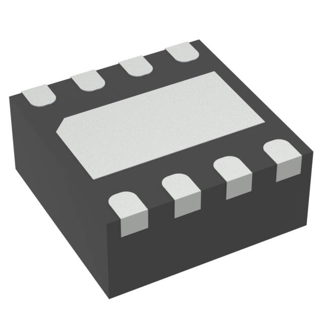
Space-Saving, 8-Lead Plastic 2 x 2 VDFN
Applications
•
•
•
•
•
Energy Harvesting
Long Life Battery-Powered Applications
Smart Cards
Ultra Low Consumption “Green” Products
Portable Electronics
The MCP1710 is stable using ceramic output
capacitors that inherently provide lower output noise,
and reduce the size and cost of the entire regulator
solution. Only 1 µF (2.2 µF recommended) of output
capacitance is needed to stabilize the LDO.
The MCP1710 device’s ultra low quiescent and
shutdown current allows it to be paired with other ultra
low-current draw devices, such as Microchip’s XLP
technology devices, for a complete ultra low-power
solution.
Package Type
MCP1710
2x2 VDFN*
8 SHDN
GND 1
VOUT 2
NC 3
NC 4
EP
9
7 VIN
6 FB
5 NC
* Includes Exposed Thermal Pad (EP); see Table 3-1.
2012-2015 Microchip Technology Inc.
DS20005158D-page 1
�MCP1710
Typical Application
+
–
CIN
COUT
SHDN
LOAD
VOUT
VIN
FB
GND
Functional Block Diagram
VIN
VOUT
Overcurrent
Voltage
Reference
+
–
SHDN
FB
SHDN
GND
DS20005158D-page 2
2012-2015 Microchip Technology Inc.
�MCP1710
1.0
ELECTRICAL CHARACTERISTICS
Absolute Maximum Ratings†
Input voltage, VIN ................................................................................................................................................6.0V
Maximum voltage on any pin – GND ..................................................................................................... 0.3V to 6.0V
Output short-circuit duration............................................................................................ ............................Unlimited
Storage temperature ....................................................................................................................... -65°C to +150°C
Maximum junction temperature, TJ ................................................................................................................ +150°C
Operating junction temperature, TJ ....................................................................................................-40°C to +85°C
ESD protection on all pins (HBM) ................................................................................................................... ≥ 2 kV
† Notice: Stresses above those listed under “Maximum Ratings” may cause permanent damage to the device. This
is a stress rating only and functional operation of the device at those or any other conditions above those indicated
in the operational listings of this specification is not implied. Exposure to maximum rating conditions for extended
periods may affect device reliability.
AC/DC CHARACTERISTICS
Electrical Specifications: Unless otherwise noted, VIN = VR + 800 mV (Note 1), IOUT = 1 mA, CIN = COUT = 2.2 µF
(X7R Ceramic), TA = +25°C. Boldface type applies for junction temperatures TJ of -40°C to +85°C (Note 4).
Parameters
Input Operating Voltage
Sym.
Min.
Typ.
Max.
Units
VIN
2.7
—
5.5
V
2.5
—
5.5
V
Conditions
VR < 2.5V
VOUT
1.2
—
4.2
V
Input Quiescent Current
IQ
—
20
—
nA
VIN = 2.5V to 5.5V,
IOUT = 0
Input Quiescent Current
for SHDN Mode
ISHDN
—
0.1
—
nA
SHDN = GND
Maximum Continuous
Output Current
IOUT
—
—
200
mA
VR ≤ 3.5V
—
—
100
mA
VR 3.5V
Current Limit
IOUT
—
250
—
mA
VOUT = 0.9 x VR,
VR ≤ 3.5V
—
175
—
mA
VOUT = 0.9 x VR,
VR 3.5V
Output Voltage Range
Output Voltage Regulation
Line Regulation
Note 1:
2:
3:
4:
VOUT
VOUT/
(VOUT x VIN)
VR – 4%
—
VR + 4%
V
VR – 2%
—
VR + 2%
V
VR < 1.8V (Note 2)
VR ≥ 1.8V (Note 2)
—
0.5
4
%
VIN = VIN(Min) to 5.5V,
VR ≥ 1.8V, IOUT = 50 mA
(Note 1)
—
—
4
%
VIN = VIN(Min) to 5.5V,
VR < 1.8V, IOUT = 50 mA
(Note 1)
The minimum VIN must meet two conditions: VIN VIN(Min) and VIN VR VDROPOUT(Max).
VR is the nominal regulator output voltage. VR = 1.2V, 2.5V, etc.
Dropout voltage is defined as the input-to-output voltage differential at which the output voltage drops 3%
below its nominal value that was measured with an input voltage of VIN = VOUT(Max) + VDROPOUT(Max).
The junction temperature is approximated by soaking the device under test at an ambient temperature
equal to the desired junction temperature. The test time is small enough such that the rise in the junction
temperature over the ambient temperature is not significant.
2012-2015 Microchip Technology Inc.
DS20005158D-page 3
�MCP1710
AC/DC CHARACTERISTICS (CONTINUED)
Electrical Specifications: Unless otherwise noted, VIN = VR + 800 mV (Note 1), IOUT = 1 mA, CIN = COUT = 2.2 µF
(X7R Ceramic), TA = +25°C. Boldface type applies for junction temperatures TJ of -40°C to +85°C (Note 4).
Parameters
Sym.
Min.
Typ.
Max.
Units
Conditions
Load Regulation
VOUT/VOUT
—
1
3
%
Dropout Voltage
VDROPOUT
—
—
450
mV
IOUT = 200 mA,
VR ≤ 3.5V (Note 3)
—
—
400
mV
IOUT = 100 mA,
VR > 3.5V (Note 3)
VIN = (VIN(Min) + VIN(Max))/2,
IOUT = 0.02 mA to 200 mA
(Note 1)
Shutdown Input
Logic High Input
VSHDN-HIGH
70
—
—
%VIN
VIN = VIN(Min) to 5.5V (Note 1)
Logic Low Input
VSHDN-LOW
—
—
30
%VIN
VIN = VIN(Min) to 5.5V (Note 1)
TOR
—
30
—
ms
eN
—
0.37
—
PSRR
—
22
—
AC Performance
Output Delay From SHDN
Output Noise
Power Supply Ripple
Rejection Ratio
Note 1:
2:
3:
4:
SHDN = GND to VIN,
VOUT = GND to 95% VR
µV/Hz IOUT = 50 mA, f = 1 kHz,
COUT = 2.2 µF (X7R Ceramic),
VR = 2.5V
dB
f = 100 Hz, IOUT = 10 mA,
VINAC = 200 mV pk-pk,
CIN = 0 µF
The minimum VIN must meet two conditions: VIN VIN(Min) and VIN VR VDROPOUT(Max).
VR is the nominal regulator output voltage. VR = 1.2V, 2.5V, etc.
Dropout voltage is defined as the input-to-output voltage differential at which the output voltage drops 3%
below its nominal value that was measured with an input voltage of VIN = VOUT(Max) + VDROPOUT(Max).
The junction temperature is approximated by soaking the device under test at an ambient temperature
equal to the desired junction temperature. The test time is small enough such that the rise in the junction
temperature over the ambient temperature is not significant.
TEMPERATURE SPECIFICATIONS
Electrical Specifications: Unless otherwise noted, VIN = VR + 800 mV, (Note 1), IOUT = 1 mA, CIN = COUT = 2.2 µF
(X7R Ceramic), TA = +25°C. Boldface type applies for junction temperatures, TJ of -40°C to +85°C (Note 4)
Parameters
Sym.
Min.
Typ.
Max.
Units
Conditions
Operating Junction
Temperature Range
TJ
-40
—
+85
°C
Steady state
Maximum Junction
Temperature
TJ
—
—
+150
°C
Transient
Storage Temperature Range
TA
-65
—
+150
°C
JA
—
73.1
—
°C/W
JC
—
10.7
—
°C/W
Temperature Ranges
Thermal Package Resistances
Thermal Resistance,
2 x 2 VDFN-8
DS20005158D-page 4
JEDEC® standard FR4 board with
1 oz copper and thermal vias
2012-2015 Microchip Technology Inc.
�MCP1710
2.0
TYPICAL PERFORMANCE CURVES
Note:
The graphs and tables provided following this note are a statistical summary based on a limited number of
samples and are provided for informational purposes only. The performance characteristics listed herein
are not tested or guaranteed. In some graphs or tables, the data presented may be outside the specified
operating range (e.g., outside specified power supply range) and therefore outside the warranted range.
Note: Unless otherwise indicated, COUT = 2.2 µF Ceramic (X7R), CIN = 2.2 µF Ceramic (X7R), IOUT = 1 mA,
Temperature = +25°C, VIN = VR + 0.8V, SHDN = 1 M pull-up to VIN.
1.240
1.205
IOUT = 0.1 mA
VIN = 2.5V
TJ = -40°C
1.200
1.230
Outtput Voltage (V)
Outtput Voltage (V)
1.235
1.225
TJ = +25°C
1.220
1.215
1.210
1.205
TJ = +85°C
1.200
TJ = +85°C
1.185
1 180
1.180
TJ = -40°C
1.170
2.5
3.0
3.5
4.0
4.5
Input Voltage (V)
5.0
5.5
FIGURE 2-1:
Output Voltage vs. Input
Voltage (VR = 1.2V).
0
50
100
150
Load Current (mA)
200
FIGURE 2-4:
Output Voltage vs. Load
Current (VR = 1.2V).
2.5025
2.510
IOUT = 0.1 mA
Ou
utput Voltage (V)
Outtput Voltage (V)
1.190
1.175
1.195
2.508
TJ = +25°C
1.195
TJ = +25°C
2.506
2.504
2.502
TJ = -40°C
2.500
TJ = +85°C
2.498
TJ = +85°C
2.5000
VIN = 3.3V
2.4975
TJ = +25°C
TJ = -40°C
2.4950
2.4925
2.496
2.4900
2.494
2.5
3.0
3.5
4.0
4.5
Input Voltage (V)
5.0
0
5.5
FIGURE 2-2:
Output Voltage vs. Input
Voltage (VR = 2.5V).
80
100
4.25
IOUT = 0.1 mA
TJ = -40°C
4.244
4.240
TJ = +25°C
TJ = +85°C
85°C
4.236
4.232
4.50
Ou
utput Voltage (V)
Ou
utput Voltage (V)
40
60
Load Current (mA)
FIGURE 2-5:
Output Voltage vs. Load
Current (VR = 2.5V).
4.252
4.248
20
VIN = 4.15V
4.24
4.23
TJ = +25°C
4.22
TJ = -40°C
TJ = +85°C
4.21
4.20
4.19
4.75
5.00
5.25
Input Voltage (V)
5.50
FIGURE 2-3:
Output Voltage vs. Input
Voltage (VR = 4.2V).
2012-2015 Microchip Technology Inc.
0
20
40
60
Load Current (mA)
80
100
FIGURE 2-6:
Output Voltage vs. Load
Current (VR = 4.2V).
DS20005158D-page 5
�MCP1710
Note: Unless otherwise indicated, COUT = 2.2 µF Ceramic (X7R), CIN = 2.2 µF Ceramic (X7R), IOUT = 1 mA,
Temperature = +25°C, VIN = VR + 0.8V, SHDN = 1 M pull-up to VIN.
0.30
0.25
TJ = +85°C
0.20
PSRR (dB)
P
Dropout Voltage (V)
VOUT = 2.5V
TJ = +25°C
0.15
TJ = -40°C
0.10
0.05
0.00
0
20
40
60
Load Current (mA)
80
100
FIGURE 2-7:
Dropout Voltage vs. Load
Current (VR = 2.5V).
VOUT = 4.2V
Drop
pout Voltage (V)
0.14
PSRR (dB)
TJ = -40°C
0.16
TJ = +85°C
0.12
0.10
TJ = +25°C
0.08
0.06
0.04
0.02
0.00
0
20
40
60
Load Current (mA)
80
100
FIGURE 2-8:
Dropout Voltage vs. Load
Current (VR = 4.2V).
0.1
PSRR (dB)
Outpu
ut Noise (μV/¥Hz)
VIN = 5.2V
VOUT = 4.2V
IOUT = 50 mA
VIN = 3.5V
VOUT = 2.5V
IOUT = 50 mA
VIN = 2.8V
VOUT = 1.8V
IOUT = 50 mA
0.01
0.01
0.1
FIGURE 2-9:
DS20005158D-page 6
1
10
100
Frequency (kHz)
1000
Noise vs. Frequency.
100
1000
10
0 VIN = 3.5V
IOUT = 10 mA
-10
-20
-30
-40
-50
-60
-70
-80
-90
-100
0.01
0.1
1
10
Frequency (kHz)
100
1000
FIGURE 2-11:
Power Supply Ripple
Rejection vs. Frequency (VR = 2.5V).
10
1
1
10
Frequency (kHz)
FIGURE 2-10:
Power Supply Ripple
Rejection vs. Frequency (VR = 1.2V).
0.20
0.18
10
0
VIN = 2.5V
-10
IOUT = 10 mA
-20
-30
-40
-50
-60
-70
-80
-90
-100
0.01
0.1
10
0 VIN = 5.2V
IOUT = 10 mA
-10
-20
-30
-40
-50
-60
-70
-80
-90
-100
0.01
0.1
1
10
Frequency (kHz)
100
1000
FIGURE 2-12:
Power Supply Ripple
Rejection vs. Frequency (VR = 4.2V).
2012-2015 Microchip Technology Inc.
�MCP1710
Note: Unless otherwise indicated, COUT = 2.2 µF Ceramic (X7R), CIN = 2.2 µF Ceramic (X7R), IOUT = 1 mA,
Temperature = +25°C, VIN = VR + 0.8V, SHDN = 1 M pull-up to VIN.
IOUT = 10 mA
VOUT = 1.2V
CH1
VIN = 2.5V to 3.5V
IOUT = 100 nA to 10 mA
CH2
VOUT = 1.2V
200 µs/div
10 ms/div
CH1 (AC) 200 mV/div
FIGURE 2-13:
(VR = 1.2V).
CH2 10 mA/div
Dynamic Load Step
2V/div
FIGURE 2-16:
(VR = 1.2V).
1V/div
Dynamic Line Step
IOUT = 10 mA
VOUT = 2.5V
VIN = 3.5V to 4.5V
VOUT = 2.5V
IOUT = 100 nA to 10 mA
200 µs/div
AC1M 200 mV/div
FIGURE 2-14:
(VR = 2.5V).
10 ms/div
10 mA/div
Dynamic Load Step
2V/div
FIGURE 2-17:
(VR = 2.5V).
1V/div
Dynamic Line Step
IOUT = 10 mA
VOUT = 4.2V
VIN = 4.5V to 5.5V
IOUT = 100 nA to 10 mA
VOUT = 4.2V
10 ms/div
200 µs/div
AC1M 200 mV/div
FIGURE 2-15:
(VR = 4.2V).
10 mA/div
Dynamic Load Step
2012-2015 Microchip Technology Inc.
2V/div
FIGURE 2-18:
(VR = 4.2V).
2V/div
Dynamic Line Step
DS20005158D-page 7
�MCP1710
Note: Unless otherwise indicated, COUT = 2.2 µF Ceramic (X7R), CIN = 2.2 µF Ceramic (X7R), IOUT = 1 mA,
Temperature = +25°C, VIN = VR + 0.8V, SHDN = 1 M pull-up to VIN.
IOUT = 10 mA
IOUT = 100 nA
SHDN Signal
VIN = 2.5V
VOUT = 1.2V
VOUT = 1.2V
10 ms/div
2V/div
FIGURE 2-19:
(VR = 1.2V).
5 ms/div
2V/div
2V/div
Start-up from VIN
FIGURE 2-22:
(VR = 1.2V).
IOUT = 100 nA
1V/div
Start-up from SHDN
IOUT = 10 mA
SHDN Signal
VIN = 3.5V
VOUT = 2.5V
VOUT = 2.5V
5 ms/div
10 ms/div
2V/div
FIGURE 2-20:
(VR = 2.5V).
2V/div
Start-up from VIN
2V/div
FIGURE 2-23:
(VR = 2.5V).
IOUT = 100 nA
1V/div
Start-up from SHDN
IOUT = 10 mA
VIN = 5.2V
SHDN Signal
VOUT = 4.2V
VOUT = 4.2V
10 ms/div
2V/div
FIGURE 2-21:
(VR = 4.2V).
DS20005158D-page 8
5 ms/div
2V/div
Start-up from VIN
2V/div
FIGURE 2-24:
(VR = 4.2V).
1V/div
Start-up from SHDN
2012-2015 Microchip Technology Inc.
�MCP1710
Note: Unless otherwise indicated, COUT = 2.2 µF Ceramic (X7R), CIN = 2.2 µF Ceramic (X7R), IOUT = 1 mA,
Temperature = +25°C, VIN = VR + 0.8V, SHDN = 1 M pull-up to VIN.
0.50
2.00
IOUT = 1 mA
0.45
1.50
Line Regulation (%/V)
Load
d Regulation (%)
IOUT = 0 mA to 100 mA
VIN = 2.5V
1.00
VIN = 4.0V
0.50
VIN = 5.5V
0.00
-0.50
-15
10
35
60
Junction Temperature (°C)
VOUT = 2.5V
0.30
0.25
VOUT = 4.2V
0.20
85
-40
50
0.30
IOUT = 0 mA to 100 mA
Quiesc
cent Current (nA)
VIN = 2.8V
0.00
-0.10
10
35
60
Junction Temperature (°C)
VIN = 4.0V
-0.20
VIN = 5.5V
-0.30
85
Line Regulation vs. Junction
VOUT = 1.2V
45
0.20
0.10
-15
FIGURE 2-28:
Temperature.
FIGURE 2-25:
Load Regulation vs.
Junction Temperature (VR = 1.2V).
Load
d Regulation (%)
0.35
0.15
-40
40
35
TJ = +85°C
30
25
20
TJ = -40°C
15
10
TJ = +25°C
5
-0.40
0
-40
-15
10
35
60
Junction Temperature (°C)
85
2.5
3.0
FIGURE 2-29:
Voltage.
FIGURE 2-26:
Load Regulation vs.
Junction Temperature (VR = 2.5V).
3.5
4.0
4.5
Input Voltage (V)
5.0
5.5
Quiescent Current vs. Input
0.95
0.05
IOUT = 0 mA to 100 mA
0.04
VIN = 5.5V
VIN = 5.0V
0.03
VIN = 2.5V
VOUT = 1.2V
IOUT = 0.1 mA
0.90
Ground Current (µA)
Load
d Regulation (%)
VOUT = 1.2V
0.40
0.02
VIN = 4.5V
0.01
0.00
0.85
0.80
0.75
0.70
0.65
0.60
0.55
0.50
-0.01
-40
-15
10
35
60
Junction Temperature (°C)
FIGURE 2-27:
Load Regulation vs.
Junction Temperature (VR = 4.2V).
2012-2015 Microchip Technology Inc.
85
-40
FIGURE 2-30:
Temperature.
-15
10
35
60
Junction Temperature (°C)
85
Ground Current vs. Junction
DS20005158D-page 9
�MCP1710
Note: Unless otherwise indicated, COUT = 2.2 µF Ceramic (X7R), CIN = 2.2 µF Ceramic (X7R), IOUT = 1 mA,
Temperature = +25°C, VIN = VR + 0.8V, SHDN = 1 M pull-up to VIN.
160
VIN = 4.0V
VOUT = 1.2V
Grou
und Current (µA)
140
TJ = +25°C
120
100
TJ = +85°C
80
TJ = -40°C
60
40
20
0
0
20
FIGURE 2-31:
Current.
DS20005158D-page 10
40
60
Load Current (mA)
80
100
Ground Current vs. Load
2012-2015 Microchip Technology Inc.
�MCP1710
3.0
PIN DESCRIPTION
The descriptions of the pins are listed in Table 3-1.
TABLE 3-1:
MCP1710
VDFN
3.1
PIN FUNCTION TABLE
Name
Description
1
GND
Ground
2
VOUT
Regulated Output Voltage
3, 4, 5
NC
Not Connected pins (should either be left floated or connected to ground)
6
FB
Output Voltage Feedback Input
7
VIN
Input Voltage Supply
8
SHDN
9
EP
Shutdown Control Input (active-low)
Exposed Thermal Pad, Connected to GND
Ground Pin (GND)
3.4
Input Voltage Supply Pin (VIN)
For optimal noise and Power Supply Rejection Ratio
(PSRR) performance, the GND pin of the LDO should
be tied to an electrically quiet circuit ground. This will
help the LDO Power Supply Rejection Ratio and noise
performance. The GND pin of the LDO only conducts
the ground current, so a heavy trace is not required.
For applications that have switching or noisy inputs, tie
the GND pin to the return of the output capacitor.
Ground planes help lower the inductance and voltage
spikes caused by fast transient load currents.
Connect the unregulated or regulated input voltage
source to VIN. If the input voltage source is located
several inches away from the LDO, or the input source
is a battery, it is recommended that an input capacitor
be used. A typical input capacitance value of 1 µF to
10 µF should be sufficient for most applications (2.2 µF,
typical). The type of capacitor used can be ceramic,
tantalum, or aluminum-electrolytic. The low-ESR
characteristics of the ceramic capacitor will yield better
noise and PSRR performance at high frequency.
3.2
3.5
Regulated Output Voltage Pin
(VOUT)
The VOUT pin is the regulated output voltage of the
LDO. A minimum output capacitance of 1.0 µF is
required for LDO stability. The MCP1710 is stable
with ceramic, tantalum and aluminum-electrolytic
capacitors. See Section 4.2 “Output Capacitor” for
output capacitor selection guidance.
3.3
Feedback Pin (FB)
The output voltage is connected to the FB input. This
sets the output voltage regulation value.
2012-2015 Microchip Technology Inc.
Shutdown Control Input (SHDN)
The SHDN input is used to turn the LDO output voltage
on and off. When the SHDN input is at a logic high
level, the LDO output voltage is enabled. When the
SHDN input is pulled to a logic low level, the LDO
output voltage is disabled. When the SHDN input is
pulled low, the LDO enters a low quiescent current
shutdown state, where the typical quiescent current is
0.1 nA.
3.6
Exposed Thermal Pad (EP)
The VDFN-8 package has an exposed thermal pad on
the bottom of the package. The exposed thermal pad
gives the device better thermal characteristics by
providing a good thermal path to either the Printed
Circuit Board (PCB), or heat sink, to remove heat from
the device. The exposed pad of the package is at
ground potential.
DS20005158D-page 11
�MCP1710
NOTES:
DS20005158D-page 12
2012-2015 Microchip Technology Inc.
�MCP1710
4.0
DEVICE OVERVIEW
The MCP1710 is a 100 mA/200 mA output current, Low
Dropout (LDO) voltage regulator. The Low Dropout
voltage of 450 mV maximum, at 200 mA of current,
makes it ideal for battery-powered applications. The input
voltage ranges from 2.5V to 5.5V. The MCP1710 adds a
shutdown control input pin. The MCP1710 is available in
eight standard fixed output voltage options: 1.2V, 1.5V,
1.8V, 2V, 2.5V, 3.0V, 3.3V and 4.2V. The MCP1710 uses
a proprietary voltage reference and sensing scheme to
maintain the ultra low 20 nA quiescent current.
4.1
Output Current and Current
Limiting
The MCP1710 LDO is tested and ensured to supply a
minimum of 200 mA of output current for the 1.2V to
3.5V output range, and 100 mA of output current for the
3.5V to 4.2V output range. The MCP1710 has no
minimum output load, so the output load current can go
to 0 mA and the LDO will continue to regulate the
output voltage within the specified tolerance.
The MCP1710 also incorporates an output current limit.
The current limit is set to 250 mA, typical, for the
1.2V VR ≤3.5V range, and 175 mA, typical, for the
3.5V VR 5.5V range.
4.2
capacitor should be placed as close to the input of the
LDO as is practical. Larger input capacitors will also
help reduce any high-frequency noise on the input and
output of the LDO, as well as the effects of any
inductance that exists between the input source
voltage and the input capacitance of the LDO.
4.4
The SHDN input is an active-low input signal that turns
the LDO on and off. The SHDN threshold is a
percentage of the input voltage. The maximum input
low logic level is 30% of VIN and the minimum high logic
level is 70% of VIN.
On the rising edge of the SHDN input, the shutdown
circuitry has a 30 ms (typical) delay before allowing the
LDO output to turn on. This delay helps to reject any
false turn-on signal or noise on the SHDN input signal.
After the 30 ms delay, the LDO output enters its
current-limited soft start period as it rises from 0V to its
final regulation value. If the SHDN input signal is pulled
low during the 30 ms delay period, the timer will be
reset and the delay time will start over again on the next
rising edge of the SHDN input. The total time from the
SHDN input going high (turn on) to the LDO output
being in regulation is typically 30 ms. See Figure 4-1 for
a timing diagram of the SHDN input.
Output Capacitor
TOR
The MCP1710 requires a minimum output capacitance
of 1 µF for output voltage stability. Ceramic capacitors
are recommended because of their size, cost and
robust environmental qualities.
Aluminum-electrolytic and tantalum capacitors can be
used on the LDO output as well. The output capacitor
should be located as close to the LDO output as is
practical. Ceramic materials, X7R and X5R, have
low-temperature coefficients and are well within the
acceptable ESR range required. A typical 1 µF X7R
0805 capacitor has an ESR of 50 m.
4.3
Shutdown Input (SHDN)
Input Capacitor
Low input source impedance is necessary for the LDO
output to operate properly. When operating from batteries,
or in applications with long lead length (>10 inches)
between the input source and the LDO, some input
capacitance is recommended. A minimum of 1.0 µF to
4.7 µF is recommended for most applications.
For applications that have output step load requirements, the input capacitance of the LDO is very
important. The input capacitance provides a
low-impedance source of current for the LDO to use for
dynamic load changes. This allows the LDO to respond
quickly to the output load step. For good step response
performance, the input capacitor should be of equivalent or higher value than the output capacitor. The
2012-2015 Microchip Technology Inc.
30 ms
20 ns (typical)
10 µs
SHDN
VOUT
FIGURE 4-1:
Diagram.
4.5
Shutdown Input Timing
Dropout Voltage
Dropout voltage is defined as the input-to-output voltage
differential at which the output voltage drops 3% below
the nominal value that was measured with a VR + 0.8V
differential applied. The MCP1710 LDO has a Low
Dropout voltage specification of 450 mV for the
1.2V VR ≤ 3.5V range (typical) at 200 mA out, and
400 mV for the 3.5V VR 5.5V range (typical) at
100 mA
out.
See
Section 1.0
“Electrical
Characteristics” for maximum dropout voltage
specifications.
DS20005158D-page 13
�MCP1710
NOTES:
DS20005158D-page 14
2012-2015 Microchip Technology Inc.
�MCP1710
5.0
APPLICATION
CIRCUITS/ISSUES
5.1
Typical Application
The MCP1710 is used for applications that require ultra
low quiescent current draw.
VOUT
VIN
SHDN
GND
LOAD
COUT
CIN
+
-
FB
The total power dissipated within the MCP1710 is the
sum of the power dissipated in the LDO pass device
and the P(IGND) term. Because of the CMOS
construction, the typical IGND for the MCP1710 is
200 µA at full load. Operating at a maximum VIN of 5.5V
results in a power dissipation of 1.1 mW. For most
applications, this is small compared to the LDO pass
device power dissipation and can be neglected.
The maximum continuous operating junction temperature specified for the MCP1710 is +85°C. To estimate the
internal junction temperature of the MCP1710, the total
internal power dissipation is multiplied by the thermal
resistance from junction-to-ambient (RJA) of the device.
The thermal resistance from junction-to-ambient for the
2 x 2 VDFN-8 package is estimated at 73.1°C/W.
EQUATION 5-3:
FIGURE 5-1:
5.2
Typical Application Circuit.
Power Calculations
5.2.1
POWER DISSIPATION
The internal power dissipation within the MCP1710 is a
function of input voltage, output voltage, output current
and quiescent current. Equation 5-1 can be used to
calculate the internal power dissipation for the LDO.
EQUATION 5-1:
P LDO = VIN MAX – V OUT MIN I OUT MAX
Where:
PLDO = Internal power dissipation of the
LDO pass device
VIN(MAX) = Maximum input voltage
T J MAX = PTOTAL R JA + T A MAX
Where:
TJ(MAX) = Maximum continuous junction
temperature
PTOTAL = Total power dissipation of the device
RJA = Thermal resistance from junction to
ambient
TA(MAX) = Maximum ambient temperature
The maximum power dissipation capability for a
package
can
be
calculated
given
the
junction-to-ambient thermal resistance and the maximum ambient temperature for the application.
Equation 5-4 can be used to determine the package
maximum internal power dissipation.
EQUATION 5-4:
VOUT(MIN) = LDO minimum output voltage
T J MAX – T A MAX
P D MAX = --------------------------------------------------R JA
IOUT(MAX) = Maximum output current
In addition to the LDO pass element power dissipation,
there is power dissipation within the MCP1710 as a
result of quiescent or ground current. The power
dissipation as a result of the ground current can be
calculated using Equation 5-2:
EQUATION 5-2:
PI GND = V IN MAX I GND
Where:
Where:
PD(MAX) = Maximum power dissipation of the
device
TJ(MAX) = Maximum continuous junction
temperature
TA(MAX) = Maximum ambient temperature
RJA = Thermal resistance from
junction-to-ambient
PI(GND) = Power dissipation due to the
quiescent current of the LDO
VIN(MAX) = Maximum input voltage
IGND = Current flowing in the GND pin
2012-2015 Microchip Technology Inc.
DS20005158D-page 15
�MCP1710
EQUATION 5-5:
T J RISE = P D MAX R JA
TJ(RISE) = Rise in the device’s junction
temperature over the ambient
temperature
PD(MAX) = Maximum power dissipation of the
device
RJA = Thermal resistance from
junction-to-ambient
EQUATION 5-6:
T J = T J RISE + T A
TJ = Junction temperature
TJ(RISE) = Rise in the device’s junction
temperature over the ambient
temperature
TA = Ambient temperature
5.3
Typical Application Examples
Internal power dissipation, junction temperature rise,
junction temperature and maximum power dissipation
are calculated in the following example. The power
dissipation, as a result of ground current, is small
enough to be neglected.
5.3.1
5.3.1.1
The internal junction temperature rise is a function of
internal power dissipation and the thermal resistance,
from junction-to-ambient, for the application. The
thermal resistance, from junction-to-ambient (RJA), is
derived from the EIA/JEDEC standards for measuring
thermal resistance. The EIA/JEDEC specification is
JESD51. The standard describes the test method and
board specifications for measuring the thermal
resistance from junction-to-ambient. The actual thermal resistance for a particular application can vary
depending on many factors, such as copper area and
thickness. Refer to AN792, “A Method to Determine
How Much Power a SOT23 Can Dissipate in an Application” (DS00792), for more information regarding this
subject.
EXAMPLE 5-2:
TJ(RISE) = PTOTAL x RJA
TJ(RISE) = 0.206W x 73.1°C/W
TJ(RISE) = 15.1°C
5.3.1.2
EXAMPLE 5-3:
TJ = TJ(RISE) + TA(MAX)
TJ = 15.1°C + 60.0°C
EXAMPLE 5-1:
TJ = 75.1°C
Package
Input Voltage
VIN = 3.3V ± 5%
LDO Output Voltage and Current
VOUT = 2.5V
IOUT = 200 mA
Maximum Ambient Temperature
TA(MAX) = +60°C
Junction Temperature Estimate
To estimate the internal junction temperature, the
calculated temperature rise is added to the ambient or
offset temperature. For this example, the worst-case
junction temperature is estimated below:
POWER DISSIPATION EXAMPLES
Package Type = 2 x 2 VDFN-8
Device Junction Temperature Rise
5.3.1.3
Maximum Package Power
Dissipation at +60°C Ambient
Temperature
EXAMPLE 5-4:
2x2 VDFN-8 (73.1°C/W RJA):
PD(MAX) = (85°C – 60°C)/73.1°C/W
PD(MAX) = 0.342W
Internal Power Dissipation
PLDO(MAX) = (VIN(MAX) – VOUT(MIN)) x IOUT(MAX)
PLDO = ((3.3V x 1.05) – (2.5V x 0.975))
x 200 mA
PLDO = 0.206 Watts
DS20005158D-page 16
2012-2015 Microchip Technology Inc.
�MCP1710
6.0
PACKAGING INFORMATION
6.1
Package Marking Information
Example
8-Lead VDFN (2 x 2 x 0.9)
Legend: XX...X
Y
YY
WW
NNN
e3
*
Note:
Part Number
Code
MCP1710T-12I/LZ
AAA
MCP1710T-15I/LZ
AAF
MCP1710T-18I/LZ
AAB
MCP1710T-20I/LZ
AAG
MCP1710T-25I/LZ
AAC
MCP1710T-30I/LZ
AAH
MCP1710T-33I/LZ
AAD
MCP1710T-42I/LZ
AAE
AAA
256
Customer-specific information
Year code (last digit of calendar year)
Year code (last 2 digits of calendar year)
Week code (week of January 1 is week ‘01’)
Alphanumeric traceability code
Pb-free JEDEC® designator for Matte Tin (Sn)
This package is Pb-free. The Pb-free JEDEC designator ( e3 )
can be found on the outer packaging for this package.
In the event the full Microchip part number cannot be marked on one line, it will
be carried over to the next line, thus limiting the number of available
characters for customer-specific information.
2012-2015 Microchip Technology Inc.
DS20005158D-page 17
�MCP1710
���/HDG�9HU\�7KLQ�'XDO�)ODWSDFN�1R�/HDG��/=��±��[�[����PP�%RG\�>9')1@
1RWH�
)RU�WKH�PRVW�FXUUHQW�SDFNDJH�GUDZLQJV��SOHDVH�VHH�WKH�0LFURFKLS�3DFNDJLQJ�6SHFLILFDWLRQ�ORFDWHG�DW
KWWS���ZZZ�PLFURFKLS�FRP�SDFNDJLQJ
'
$
%
1
�'$780�$�
�'$780�%�
(
�;
���� &
�
�
127(��
�;
���� &
723�9,(:
���� &
$
&
6($7,1*
3/$1(
�;
�$��
6,'(�9,(:
'�
�
���� &
$�
6((�'(7$,/�%
�
(�
.
1
/
H
�;�E
����
����
& $ %
&
%27720�9,(:
0LFURFKLS�7HFKQRORJ\�'UDZLQJ��&������%�6KHHW���RI��
DS20005158D-page 18
2012-2015 Microchip Technology Inc.
�MCP1710
���/HDG�9HU\�7KLQ�'XDO�)ODWSDFN�1R�/HDG��/=��±��[�[����PP�%RG\�>9')1@
1RWH�
)RU�WKH�PRVW�FXUUHQW�SDFNDJH�GUDZLQJV��SOHDVH�VHH�WKH�0LFURFKLS�3DFNDJLQJ�6SHFLILFDWLRQ�ORFDWHG�DW
KWWS���ZZZ�PLFURFKLS�FRP�SDFNDJLQJ
H
H��
�'$780�$�
'(7$,/�%
8QLWV
'LPHQVLRQ�/LPLWV
1
1XPEHU�RI�3LQV
H
3LWFK
$
2YHUDOO�+HLJKW
6WDQGRII
$�
�$��
7HUPLQDO�7KLFNQHVV��5()�
2YHUDOO�:LGWK
'
([SRVHG�3DG�:LGWK
'�
2YHUDOO�/HQJWK
(
([SRVHG�3DG�/HQJWK
(�
E
7HUPLQDO�:LGWK
7HUPLQDO�/HQJWK
/
7HUPLQDO�WR�([SRVHG�3DG
.
0,1
����
����
����
����
����
����
����
0,//,0(7(56
120
�
�����%6&
����
����
������5()�
�����%6&
����
�����%6&
����
����
����
�
0$;
����
����
����
����
����
����
�
1RWHV�
�� 3LQ���YLVXDO�LQGH[�IHDWXUH�PD\�YDU\��EXW�PXVW�EH�ORFDWHG�ZLWKLQ�WKH�KDWFKHG�DUHD�
�� 3DFNDJH�PD\�KDYH�RQH�RU�PRUH�H[SRVHG�WLH�EDUV�DW�HQGV�
�� 3DFNDJH�LV�VDZ�VLQJXODWHG
�� 'LPHQVLRQLQJ�DQG�WROHUDQFLQJ�SHU�$60(�


 工商网监
湘ICP备2023018690号
工商网监
湘ICP备2023018690号

