MCP1711
150 mA Ultra-Low Quiescent Current, Capacitorless LDO Regulator
Features
General Description
• Low Quiescent Current: 600 nA
• Input Voltage Range: 1.4V to 6.0V
• Standard Output Voltages: 1.2V, 1.8V, 1.9V, 2.0V,
2.2V, 2.5V, 3.0V, 3.3V, 5.0V
• Output Accuracy: ±20 mV for 1.2V and 1.8V
Options and ±1% for VR 2.0V
• Temperature Stability: ±50 ppm/°C
• Maximum Output Current: 150 mA
• Low ON Resistance: 3.3 @ VR = 3.0V
• Standby Current: 10 nA
• Protection Circuits: Current Limiter, Short Circuit,
Foldback
• SHDN Pin Function: ON/OFF Logic = Enable
High
• COUT Discharge Circuit when SHDN Function is
Active
• Output Capacitor: Low Equivalent Series
Resistance (ESR) Ceramic, Capacitorless
Compatible
• Operating Temperature: -40°C to +85°C
(Industrial)
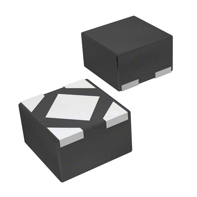
• Available Packages:
- 4-Lead 1 x 1 mm UQFN
- 5-Lead SOT-23
• Environmentally Friendly: EU RoHS Compliant,
Lead-Free
The MCP1711 is a highly accurate CMOS low dropout
(LDO) voltage regulator that can deliver up to 150 mA
of current while consuming only 0.6 µA of quiescent
current (typical). The input operating range is specified
from 1.4V to 6.0V, making it an ideal choice for mobile
applications and one-cell Li-Ion powered applications.
Applications
•
•
•
•
•
•
•
Energy Harvesting
Long-Life, Battery-Powered Applications
Portable Electronics
Ultra-Low Consumption “Green” Products
Mobile Devices/Terminals
Wireless LAN
Modules (Wireless, Cameras)
Related Literature
• AN765, Using Microchip’s Micropower LDOs
(DS00765), Microchip Technology Inc.
• AN766, Pin-Compatible CMOS Upgrades to Bipolar
LDOs (DS00766), Microchip Technology Inc.
• AN792, A Method to Determine How Much Power
a SOT23 Can Dissipate in an Application
(DS00792), Microchip Technology Inc.
2015-2016 Microchip Technology Inc.
The MCP1711 is capable of delivering 150 mA output
current with only 0.32V (typical) for VR = 5.0V, and
1.41V (typical) for VR = 1.2V of input-to-output voltages
differential. The output voltage accuracy of the
MCP1711 is typically ± 0.02V for VR < 2.0V and ±1% for
VR 2.0V at +25°C. The temperature stability is
approximately ±50 ppm/°C. Line regulation is
±0.01%/V typical at +25°C.
The output voltages available for the MCP1711 range
from 1.2V to 5.0V. The LDO output is stable even if an
output capacitor is not connected, due to an excellent
internal phase compensation. However, for better transient responses, the output capacitor should be added.
The MCP1711 is compatible with low ESR ceramic
output capacitors.
Overcurrent limit and short-circuit protection embedded into the device provide a robust solution for any
application.
The MCP1711 has a true current foldback feature.
When the load decreases beyond the MCP1711 load
rating, the output current and output voltage will
foldback toward 80 mA (typical) at approximately 0V
output. When the load impedance increases and
returns to the rated load, the MCP1711 will follow the
same foldback curve as the device comes out of
current foldback.
If the device is in Shutdown mode, by inputting a
low-level signal to the SHDN pin, the current
consumption is reduced to less than 0.1 µA (typically
0.01 µA). In Shutdown mode, if the output capacitor is
used, it will be discharged via the internal dedicated
switch and, as a result, the output voltage quickly
returns to 0V.
The package options for the MCP1711 are the 4-lead
1 x 1 mm UQFN and the 5-lead SOT-23, which make
the device ideal for small and compact applications.
DS20005415D-page 1
�MCP1711
Package Types
Typical Application Circuit
MCP1711
1x1 UQFN*
Top View
VIN
4
MCP1711
SOT-23
Top View
VOUT
5
SHDN
3
MCP1711
1x1 UQFN and SOT-23
NC
4
MCP1711
VIN
VIN
CIN
EP
5
1
VOUT
COUT
0.1 µF
Ceramic
2
1
3
VIN GND SHDN
2
GND
VOUT
VOUT
ON
OFF
SHDN
GND
* Includes Exposed Thermal Pad (EP);
see Table 3-1
Functional Block Diagram
PMOS
VIN
VOUT
Current
Limit
Ref
–
R1
Err Amp
+
DT
SHDN
DS20005415D-page 2
ON/OFF
Control
SHDN to each block
R2
RDCHG
Discharge transistor (DT)
2015-2016 Microchip Technology Inc.
�MCP1711
1.0
ELECTRICAL CHARACTERISTICS
Absolute Maximum Ratings †
Input Voltage, VIN .....................................................................................................................................................+6.5V
VIN, SHDN.................................................................................................................................................. -0.3V to +6.5V
Output Current, IOUT (1) .........................................................................................................................................470 mA
Output Voltage, VOUT (2)....................................................................................................... -0.3V to VIN + 0.3V or +6.5V
Power Dissipation
5-Lead SOT-23 ..................................................... 600 mW (JEDEC 51-7 FR-4 board with thermal vias) or 250 mW (3)
4-Lead 1 x 1 mm UQFN ........................................ 550 mW (JEDEC 51-7 FR-4 board with thermal vias) or 100 mW (3)
Storage Temperature .............................................................................................................................. -55°C to +125°C
Operating Ambient Temperature ............................................................................................................... -40°C to +85°C
ESD Protection on all pins ...........................................................................................................±1 kV HBM, ±200V MM
† Notice: Stresses above those listed under “Absolute Maximum Ratings” may cause permanent damage to the device.
This is a stress rating only and functional operation of the device at those or any other conditions above those indicated
in the operational sections of this specification is not intended. Exposure to maximum rating conditions for extended
periods may affect device reliability.
Note 1: Provided that the device is used in the range of IOUT PD/(VIN - VOUT).
2: The maximum rating corresponds to the lowest value between VIN + 0.3V or +6.5V.
3: The device is mounted on one layer PCB with minimal copper that does not provide any additional cooling.
DC CHARACTERISTICS
Electrical Characteristics: Unless otherwise indicated, VSHDN = VIN, IOUT = 1 mA, CIN = COUT = 0 µF, VIN = 3.5V for
VR < 2.5V and VIN = VR + 1V for VR 2.5V, TA = +25°C
Parameters
Sym.
Min.
Typ.
Max.
Units
Conditions
VIN
1.4
—
6.0
V
IOUT = 1 µA
VOUT
VR - 0.02
VR
VR + 0.02
V
VR < 2.0V
VR x 0.99
VR
VR x 1.01
IOUT
150
—
—
mA
VOUT
-16
±3
+16
mV
-50
±17
+50
Input-Output Characteristics
Input Voltage
Output Voltage
Maximum Output Current
Load Regulation
Dropout Voltage
(1)
Input Quiescent Current
Input Quiescent Current
for SHDN mode
Line Regulation
Note 1:
2:
VDROPOUT1
—
VDROP1
(2)
VDROP2
(2)
VR 2.0V
1 µA IOUT 1 mA
1 mA IOUT 150 mA
V
IOUT = 50 mA
VDROPOUT2
—
IOUT = 150 mA
Iq
—
0.60
1.27
—
0.65
1.50
1.9V VR < 4.0V
—
0.80
1.80
VR 4.0V
ISHDN
—
0.01
0.10
µA
VIN = 6.0V
VSHDN = VIN
VOUT/
(VIN x VOUT)
-0.13
±0.01
+0.13
%/V
IOUT = 1 µA
VR + 0.5V VIN 6.0V
-0.19
±0.01
+0.19
µA
VR < 1.9V
IOUT = 1 mA
VR 1.2V,VR + 0.5V VIN
6.0V
The dropout voltage is defined as the input to output differential at which the output voltage drops 2%
below the output voltage value that was measured with an applied input voltage of VIN = VR + 1V.
VDROP1, VDROP2: Dropout Voltage (Refer to the DC Characteristics Voltage Table).
2015-2016 Microchip Technology Inc.
DS20005415D-page 3
�MCP1711
DC CHARACTERISTICS (CONTINUED)
Electrical Characteristics: Unless otherwise indicated, VSHDN = VIN, IOUT = 1 mA, CIN = COUT = 0 µF, VIN = 3.5V for
VR < 2.5V and VIN = VR + 1V for VR 2.5V, TA = +25°C
Parameters
Sym.
Min.
Typ.
Max.
VOUT/
(T x VOUT)
—
±50
—
ILIMIT
150
270
—
mA
VOUT = 0.95 x VR
Output Short-Circuit
Foldback Current
IOUT_SC
—
80
—
mA
VOUT = GND
COUT Auto-Discharge
Resistance
RDCHG
280
450
640
SHDN = GND
VOUT = VR
en
—
30
—
SHDN Logic High Input
Voltage
VSHDN-HIGH
0.91
—
6.00
V
SHDN Logic Low Input
Voltage
VSHDN-LOW
0
—
0.38
V
SHDN High-Level Current
ISHDN-HIGH
-0.1
—
+0.1
µA
VIN = 6.0V
SHDN Low-Level Current
ISHDN-LOW
-0.1
—
+0.1
µA
VIN = 6.0V
SHDN = GND
Output Voltage
Temperature Stability
Current Limit
Noise
Units
Conditions
ppm/°C IOUT = 10 mA
-40°C TA +85°C
µV(rms) CIN = COUT = 1 µF, IOUT = 50
mA, f = 10 Hz to 100 kHz
Shutdown Input
Note 1:
2:
The dropout voltage is defined as the input to output differential at which the output voltage drops 2%
below the output voltage value that was measured with an applied input voltage of VIN = VR + 1V.
VDROP1, VDROP2: Dropout Voltage (Refer to the DC Characteristics Voltage Table).
DC CHARACTERISTICS VOLTAGE TABLE
Nominal
Output
Voltage
Output Voltage (V)
VOUT
Dropout Voltage (V)
VDROP1
VDROP1
VDROP2
VDROP2
VR (V)
Min.
Max.
Typ.
Max.
Typ.
Max.
1.2
1.1800
1.2200
0.87
1.23
1.41
1.93
1.8
1.7800
1.8200
0.47
0.72
0.99
1.40
1.9
1.8800
1.9200
0.42
0.64
0.92
1.29
2.0
1.9800
2.0200
0.37
0.58
0.86
1.20
2.2
2.1780
2.2220
0.31
0.47
0.75
1.05
2.5
2.4750
2.5250
0.26
0.40
0.67
0.92
3.0
2.9700
3.0300
0.17
0.26
0.50
0.67
3.3
3.2670
3.3330
0.17
0.26
0.50
0.67
5.0
4.9500
5.0500
0.10
0.16
0.32
0.43
DS20005415D-page 4
2015-2016 Microchip Technology Inc.
�MCP1711
TEMPERATURE SPECIFICATIONS (Note 1)
Parameters
Sym.
Min.
Typ.
Max.
Units
Conditions
TA
-40
—
+85
°C
Junction Operating Temperature
TJ
-40
—
+125
°C
Storage Temperature Range
TA
-55
—
+125
°C
JA
—
181.82
—
°C/W JEDEC 51-7 FR4 board with
thermal vias
Temperature Ranges
Operating Ambient Temperature Range
Package Thermal Resistances
Thermal Resistance, 1 x 1 UQFN-4Ld
Thermal Resistance, SOT-23-5Ld
Note 1:
2:
JA
—
1000
—
°C/W Note 2
JC
—
15
—
°C/W
JA
—
166.67
—
°C/W JEDEC 51-7 FR4 board with
thermal vias
JA
—
400
—
°C/W Note 2
JC
—
81
—
°C/W
The maximum allowable power dissipation is a function of ambient temperature, the maximum allowable
junction temperature, and the thermal resistance from junction to air (i.e., TA, TJ, JA). Exceeding the maximum allowable power dissipation will cause the device operating junction temperature to exceed the
maximum +125°C rating. Sustained junction temperatures above +125°C can impact the device reliability.
The device is mounted on one layer PCB with minimal copper that does not provide any additional cooling.
2015-2016 Microchip Technology Inc.
DS20005415D-page 5
�MCP1711
2.0
TYPICAL PERFORMANCE CURVES
Note:
The graphs and tables provided following this note are a statistical summary based on a limited number of
samples and are provided for informational purposes only. The performance characteristics listed herein
are not tested or guaranteed. In some graphs or tables, the data presented may be outside the specified
operating range (e.g., outside specified power supply range) and therefore outside the warranted range.
NOTE: Unless otherwise indicated, VIN = 3.5V for VR < 2.5V or VIN = VR + 1V for VR 2.5V, IOUT = 1 mA,
CIN = COUT = 0 µF, VSHDN = VIN, TA = +25°C.
1.20
1.20
VR = 5.0V
Quiescent Current (µA)
Quiescent Current (µA)
VR = 1.2V
1.00
0.80
TA = +85°C
TA = +25°C
0.60
0.40
TA = -40°C
0.20
0.00
1.00
TA = +85°C
TA = +25°C
0.80
0.60
0.40
TA = -40°C
0.20
0.00
0
1
2
3
4
5
6
0
1
Input Voltage (V)
FIGURE 2-1:
Voltage.
FIGURE 2-4:
Voltage.
1.2
45
1
0.8
TA = +85°C
0.6
0.4
TA = -40°C
1
2
3
4
5
35
30
25
20
15
10
0
6
Quiescent Current vs. Input
0
30
45
VR = 3.3V
TA = +85°C
0.60
TA = +25°C
TA = -40°C
0.20
60
90
Load Current (mA)
120
150
Ground Current vs. Load
VR = 1.8V
40
0.80
0.40
FIGURE 2-5:
Current.
Ground Current (µA)
Quiescent Current (µA)
1.20
1.00
6
Quiescent Current vs. Input
Input Voltage (V)
FIGURE 2-2:
Voltage.
5
5
0
0
4
VR = 1.2V
40
Ground Current (µA)
Quiescent Current (µA)
VR = 1.8V
TA = +25°C
3
Input Voltage (V)
Quiescent Current vs. Input
0.2
2
35
30
25
20
15
10
5
0.00
0
1
2
3
4
5
6
0
0
Input Voltage (V)
FIGURE 2-3:
Voltage.
DS20005415D-page 6
Quiescent Current vs. Input
FIGURE 2-6:
Current.
30
60
90
Load Current (mA)
120
150
Ground Current vs. Load
2015-2016 Microchip Technology Inc.
�MCP1711
Note: Unless otherwise indicated, VIN = 3.5V for VR < 2.5V or VIN = VR + 1V for VR 2.5V, IOUT = 1 mA,
CIN = COUT = 0 µF, VSHDN = VIN, TA = +25°C.
.
40
VR = 3.3V
Ground Current (µA)
35
3.5V
30
25
VIN
0V
tr = 5 µs
20
VOUT (DC Coupled, 1V/Div)
15
IOUT = 1 µA
10
5
VOUT
IOUT = 10 mA
0
0
30
60
90
Load Current (mA)
FIGURE 2-7:
Current.
120
VR = 1.8V
Time = 80 µs/Div
150
Ground Current vs. Load
IOUT = 150 mA
FIGURE 2-10:
Start-Up from VIN.
45
VR = 5.0V
Ground Current (µA)
40
4.3V
35
30
VIN
25
0V
tr = 5 µs
VOUT (DC Coupled, 1V/Div)
IOUT = 1 µA
20
15
10
IOUT = 150 mA
5
IOUT = 10 mA
VOUT
0
0
30
60
90
120
VR = 3.3V
Time = 80 µs/Div
150
Load Current (mA)
FIGURE 2-8:
Current.
Ground Current vs. Load
Start-Up from VIN.
FIGURE 2-11:
3.5V
VIN
0V
tr = 5 µs
6.0 V
VIN
IOUT = 1 µA
IOUT = 10 mA
VOUT
VOUT (DC Coupled, 0.5V/Div)
IOUT = 150 mA
Time = 80 µs/Div
FIGURE 2-9:
Start-Up from VIN.
2015-2016 Microchip Technology Inc.
0V
tr = 5 µs
VOUT
VR = 1.2V
VOUT (DC Coupled, 2V/Div)
IOUT = 1 µA
IOUT = 10 mA
IOUT = 150 mA
VR = 5.0V
Time = 80 µs/Div
FIGURE 2-12:
Start-Up from VIN.
DS20005415D-page 7
�MCP1711
Note: Unless otherwise indicated, VIN = 3.5V for VR < 2.5V or VIN = VR + 1V for VR 2.5V, IOUT = 1 mA,
CIN = COUT = 0 µF, VSHDN = VIN, TA = +25°C.
6.0 V
3.5V
VIN
0V
VIN
tr = 5 µs
VOUT (DC Coupled, 0.5V/Div)
IOUT = 10 mA
IOUT = 100 mA
VOUT
Time = 80 µs/Div
VR = 1.2V
CIN = COUT = 1 µF
Start-Up from VIN.
IOUT
IOUT = 150 mA
0V
VR = 5.0V
CIN = COUT = 1 µF
Time = 80 µs/Div
FIGURE 2-16:
3.5V
VIN
VOUT (DC Coupled, 2V/Div)
IOUT = 10 mA
IOUT = 100 mA
IOUT = 150 mA
FIGURE 2-13:
0V tr = 5 µs
Start-Up from VIN.
3.5V
tr = 5 µs
EN
0V
tr = 5 µs
VOUT (DC Coupled, 1V/Div)
VOUT (DC Coupled, 0.5V/Div)
IOUT = 1 µA
IOUT = 10 mA
IOUT = 100 mA
VOUT
IOUT = 150 mA
Time = 80 µs/Div
FIGURE 2-14:
VR = 1.8V
CIN = COUT = 1 µF
Start-Up from VIN.
IOUT = 150 mA
VOUT
IOUT = 10 mA
FIGURE 2-17:
4.3V
VIN
0V
IOUT = 10 mA
VOUT (DC Coupled, 1V/Div)
SHDN
0V
tr = 5 µs
VOUT (DC Coupled, 1V/Div)
IOUT = 100 mA
IOUT = 1 µA
IOUT = 150 mA
Time = 80 µs/Div
FIGURE 2-15:
DS20005415D-page 8
Start-Up from SHDN.
3.5V
tr = 5 µs
VOUT
VR = 1.2V
Time = 80 µs/Div
VR = 3.3V
CIN = COUT = 1 µF
Start-Up from VIN.
VOUT
IOUT = 10 mA
Time = 80 µs/Div
FIGURE 2-18:
IOUT = 150 mA
VR = 1.8V
Start-Up from SHDN.
2015-2016 Microchip Technology Inc.
�MCP1711
Note: Unless otherwise indicated, VIN = 3.5V for VR < 2.5V or VIN = VR + 1V for VR 2.5V, IOUT = 1 mA,
CIN = COUT = 0 µF, VSHDN = VIN, TA = +25°C.
SHDN
0V
tr = 5 µs
VOUT (DC Coupled, 1V/Div)
IOUT = 1 µA
IOUT = 150 mA
IOUT = 10 mA
VOUT
Output Voltage (V)
4.3V
2.00
1.80
1.60
1.40
1.20
1.00
0.80
0.60
0.40
0.20
0.00
VR = 3.3V
Time = 80 µs/Div
VR = 1.8V
VIN = 2.5V
VIN = 6.0V
VIN = 4.5V
VIN = 3.5V
0
50
100
150
200
250
300
Output Current (mA)
FIGURE 2-19:
Start-Up from SHDN.
FIGURE 2-22:
Current.
Output Voltage vs. Output
3.50
VR = 3.3V
6.0 V
tr = 5 µs
SHDN 0V
VOUT (DC Coupled, 2V/Div)
IOUT = 1 µA
Output Voltage (V)
3.00
VIN = 5.0V
VIN = 3.6V
2.00
VIN = 4.3V
VIN = 6.0V
1.50
1.00
0.50
IOUT = 150 mA
VOUT
2.50
IOUT = 10 mA
0.00
0
VR = 5.0V
Time = 80 µs/Div
50
100
150
200
250
300
350
Output Current (mA)
FIGURE 2-20:
1.40
VR = 1.2V
1.20
VIN = 3.5V
VIN = 2.5V
1.00
Output Voltage (V)
Output Voltage (V)
FIGURE 2-23:
Current.
Start-Up from SHDN.
VIN = 4.5V
0.80
VIN = 6.0V
0.60
0.40
0.20
0.00
0
50
100
150
200
250
5.50
5.00
4.50
4.00
3.50
3.00
2.50
2.00
1.50
1.00
0.50
0.00
VR = 5.0V
VIN = 5.5V
VIN = 6.0V
VIN = 5.2V
0
50
Output Current (mA)
FIGURE 2-21:
Current.
Output Voltage vs. Output
2015-2016 Microchip Technology Inc.
Output Voltage vs. Output
100
150
200
250
300
350
400
Output Current (mA)
FIGURE 2-24:
Current.
Output Voltage vs. Output
DS20005415D-page 9
�MCP1711
Note: Unless otherwise indicated, VIN = 3.5V for VR < 2.5V or VIN = VR + 1V for VR 2.5V, IOUT = 1 mA,
CIN = COUT = 0 µF, VSHDN = VIN, TA = +25°C.
1.40
VR = 1.2V
1.00
Output Voltage (V)
Output Voltage (V)
1.20
TA = +85°C
0.80
TA = +25°C
0.60
TA = -40°C
0.40
0.20
0.00
0
50
100
150
200
5.50
5.00
4.50
4.00
3.50
3.00
2.50
2.00
1.50
1.00
0.50
0.00
VR = 5.0V
TA = +85°C
TA = -40°C
TA = +25°C
0
250
50
Output Current (mA)
Output Voltage vs. Output
2.00
1.80
1.60
1.40
1.20
1.00
0.80
0.60
0.40
0.20
0.00
FIGURE 2-28:
Current.
200
250
300
350
Output Voltage vs. Output
1.40
VR = 1.8V
VR = 1.2V
1.20
TA = +85°C
TA = +25°C
1.00
IOUT = 1 µA
0.80
IOUT = 1 mA
0.60
IOUT = 10 mA
0.40
IOUT = 100 mA
0.20
TA = -40°C
0.00
0
50
100
150
200
250
300
0
1
Output Current (mA)
FIGURE 2-26:
Current.
Output Voltage vs. Output
FIGURE 2-29:
Voltage.
Output Voltage (V)
VR = 3.3V
3.00
2.50
2.00
TA = +85°C
1.50
TA = -40°C
TA = +25°C
1.00
0.50
0.00
0
50
100
150
200
250
300
350
2.00
1.80
1.60
1.40
1.20
1.00
0.80
0.60
0.40
0.20
0.00
DS20005415D-page 10
3
4
5
6
Output Voltage vs. Output
Output Voltage vs. Input
VR = 1.8V
IOUT = 100 mA
IOUT = 10 mA
IOUT = 1 mA
IOUT = 1 µA
0
1
Output Current (mA)
FIGURE 2-27:
Current.
2
Input Voltage (V)
3.50
Output Voltage (V)
150
Output Current (mA)
Output Voltage (V)
Output Voltage (V)
FIGURE 2-25:
Current.
100
2
3
4
5
6
Input Voltage (V)
FIGURE 2-30:
Voltage.
Output Voltage vs. Input
2015-2016 Microchip Technology Inc.
�MCP1711
Note: Unless otherwise indicated, VIN = 3.5V for VR < 2.5V or VIN = VR + 1V for VR 2.5V, IOUT = 1 mA,
CIN = COUT = 0 µF, VSHDN = VIN, TA = +25°C.
3.50
VR = 3.3V
Output Voltage (V)
Output Voltage (V)
3.00
IOUT = 100 mA
2.50
2.00
IOUT = 10 mA
1.50
1.00
IOUT = 1 mA
0.50
IOUT = 1 µA
0.00
0
1
2
3
4
Input Voltage (V)
5.50
5.00
4.50
4.00
3.50
3.00
2.50
2.00
1.50
1.00
0.50
0.00
VR = 1.8V
IOUT = 1 µA
-15
3.60
IOUT = 100 mA
IOUT = 10 mA
IOUT = 1 mA
4
5
3.45
3.40
IOUT = 1 mA
3.35
3.30
-15
10
35
60
Ambient Temperature (°C)
5.20
IOUT = 10 mA
IOUT = 1 mA
IOUT = 1 µA
85
Output Voltage vs. Ambient
VR = 5.0V
5.15
Output Voltage (V)
Output Voltage (V)
FIGURE 2-35:
Temperature.
VR = 1.2V
IOUT = 100 mA
IOUT = 10 mA
-40
6
Output Voltage vs. Input
IOUT = 100 mA
Output Voltage vs. Ambient
IOUT = 1 µA
Input Voltage (V)
1.25
1.24
1.23
1.22
1.21
1.20
1.19
1.18
1.17
1.16
1.15
85
3.50
3.20
FIGURE 2-32:
Voltage.
60
3.25
IOUT = 1 µA
3
35
VR = 3.3V
3.55
2
10
FIGURE 2-34:
Temperature.
Output Voltage vs. Input
1
IOUT = 10 mA
Ambient Temperature (°C)
5.0V
VVRR == 5.0V
0
IOUT = 100 mA
IOUT = 1 mA
-40
6
Output Voltage (V)
Output Voltage (V)
FIGURE 2-31:
Voltage.
5
1.85
1.84
1.83
1.82
1.81
1.80
1.79
1.78
1.77
1.76
1.75
IOUT = 1 µA
5.10
IOUT = 1 mA
5.05
5.00
4.95
IOUT = 10 mA
4.90
IOUT = 100 mA
4.85
4.80
-40
-15
10
35
60
85
-40
Output Voltage vs. Ambient
2015-2016 Microchip Technology Inc.
10
35
60
85
Ambient Temperature (°C)
Ambient Temperature (°C)
FIGURE 2-33:
Temperature.
-15
FIGURE 2-36:
Temperature.
Output Voltage vs. Ambient
DS20005415D-page 11
�MCP1711
Note: Unless otherwise indicated, VIN = 3.5V for VR < 2.5V or VIN = VR + 1V for VR 2.5V, IOUT = 1 mA,
CIN = COUT = 0 µF, VSHDN = VIN, TA = +25°C.
450
VR = 1.2V
1600
1400
TA = +25°C
1200
1000
800
600
VR = 5.0V
400
TA = +85°C
Dropout Voltage (mV)
Dropout Voltage (mV)
1800
TA = -40°C
400
TA = +85°C
350
300
250
200
TA = +25°C
150
100
200
TA = -40°C
50
0
0
0
25
50
75
100
125
150
0
25
50
Output Current (mA)
Dropout Voltage vs. Output
Dropout Voltage (mV)
1400
VR = 1.8V
1200
TA = +85°C
1000
800
TA = +25°C
600
400
200
TA = -40°C
FIGURE 2-40:
Current.
0
25
FIGURE 2-38:
Current.
Dropout Voltage (mV)
150
Dropout Voltage vs. Output
VR = 1.2V to 5.0V
SHDN High Level
0.80
0.60
SHDN Low Level
0.40
0.20
50
75
100
125
150
-40
-15
Dropout Voltage vs. Output
VR = 3.3V
TA = +85°C
TA = -40°C
75
100
60
85
4.5V
TA = +25°C
50
35
FIGURE 2-41:
Shutdown Threshold
Voltage vs. Ambient Temperature.
VIN
25
10
Ambient Temperature (°C)
Output Current (mA)
0
125
0.00
0
500
450
400
350
300
250
200
150
100
50
0
100
1.00
SHDN Threshold Voltage (V)
FIGURE 2-37:
Current.
75
Load Current (mA)
3.5V
tf = 5 µs
tr = 5 µs
VOUT (AC Coupled, 500 mV/Div)
VOUT
125
150
VR = 1.2V
VIN = 3.5V to 4.5V
IOUT = 10 mA
Time = 80 µs/Div
Load Current (mA)
FIGURE 2-39:
Current.
DS20005415D-page 12
Dropout Voltage vs. Output
FIGURE 2-42:
Dynamic Line Response.
2015-2016 Microchip Technology Inc.
�MCP1711
Note: Unless otherwise indicated, VIN = 3.5V for VR < 2.5V or VIN = VR + 1V for VR 2.5V, IOUT = 1 mA,
CIN = COUT = 0 µF, VSHDN = VIN, TA = +25°C.
4.5V
VIN
3.5V
5.3V
VIN
tf = 5 µs
tr = 5 µs
4.3V
tr = 5 µs
tf = 5 µs
VOUT (AC Coupled, 500 mV/Div)
VOUT (AC Coupled, 500 mV/Div)
VOUT
VOUT
VR = 1.2V
VIN = 3.5V to 4.5V
IOUT = 100 mA
VR = 3.3V
VIN = 4.3V to 5.3V
IOUT = 10 mA
FIGURE 2-43:
Time = 80 µs/Div
Dynamic Line Response.
FIGURE 2-46:
3.5V
Dynamic Line Response.
5.3V
4.5V
VIN
Time = 80 µs/Div
VIN
tf = 5 µs
tr = 5 µs
4.3V
tr = 5 µs
tf = 5 µs
VOUT (AC Coupled, 500 mV/Div)
VOUT (AC Coupled, 500 mV/Div)
VOUT
VOUT
VR = 1.8V
VIN = 3.5V to 4.5V
IOUT = 10 mA
VR = 3.3V
VIN = 4.3V to 5.3V
IOUT = 100 mA
FIGURE 2-44:
Time = 80 µs/Div
Dynamic Line Response.
FIGURE 2-47:
3.5V
Dynamic Line Response.
6.0V
4.5V
VIN
Time = 80 µs/Div
VIN
tf = 5 µs
tr = 5 µs
5.2V
tr = 5 µs
tf = 5 µs
VOUT (AC Coupled, 500 mV/Div)
VOUT (AC Coupled, 500 mV/Div)
VOUT
VOUT
VR = 1.8V
VIN = 3.5V to 4.5V
IOUT = 100 mA
VR = 5.0V
VIN = 5.2V to 6.0V
IOUT = 10 mA
FIGURE 2-45:
Time = 80 µs/Div
Dynamic Line Response.
2015-2016 Microchip Technology Inc.
FIGURE 2-48:
Time = 80 µs/Div
Dynamic Line Response.
DS20005415D-page 13
�MCP1711
Note: Unless otherwise indicated, VIN = 3.5V for VR < 2.5V or VIN = VR + 1V for VR 2.5V, IOUT = 1 mA,
CIN = COUT = 0 µF, VSHDN = VIN, TA = +25°C.
150 mA
6.0V
VIN
5.5V
tr = 5 µs
IOUT
tf = 5 µs
tr1
tf = 5 µs
1 mA
VOUT (AC Coupled, 500 mV/Div)
VOUT (AC Coupled, 1V/Div)
VOUT
VOUT
VR = 5.0V
VIN = 5.5V to 6.0V
IOUT = 100 mA
Time = 80 µs/Div
Time = 200 µs/Div
1
FIGURE 2-49:
Dynamic Line Response.
tr set time = 5 µs
FIGURE 2-52:
150 mA
IOUT
tr
tr1
tf = 5 µs
VOUT (AC Coupled, 1V/Div)
VOUT
Time = 200 µs/Div
VR = 1.2V
VIN = 3.5V
IOUT = 1 µA to 150 mA
VOUT
VR = 1.2V
VIN = 3.5V
IOUT = 1 mA to 150 mA
Time = 200 µs/Div
tr set time = 5 µs
1
FIGURE 2-50:
Dynamic Load Response.
150 mA
1
CIN = COUT = 1 µF
tf = 5 µs
IOUT
VOUT (AC Coupled, 1V/Div)
IOUTtr
Dynamic Load Response.
150 mA
1
1 µA
1
VR = 1.2V
VIN = 3.5V
IOUT = 1 mA to 150 mA
FIGURE 2-53:
CIN = COUT = 1 µF
tf = 5 µs
tr set time = 5 µs
Dynamic Load Response.
150 mA
IOUT
tr1
tf = 5 µs
1 µA
1 µA
VOUT (AC Coupled, 1V/Div)
VOUT (AC Coupled, 1V/Div)
VOUT
Time = 200 µs/Div
1
VR = 1.2V
VIN = 3.5V
IOUT = 1 µA to 150 mA
DS20005415D-page 14
Time = 200 µs/Div
1
tr set time = 5 µs
FIGURE 2-51:
VOUT
Dynamic Load Response.
VR = 1.8V
VIN = 3.5V
IOUT = 1 µA to 150 mA
tr set time = 5 µs
FIGURE 2-54:
Dynamic Load Response.
2015-2016 Microchip Technology Inc.
�MCP1711
Note: Unless otherwise indicated, VIN = 3.5V for VR < 2.5V or VIN = VR + 1V for VR 2.5V, IOUT = 1 mA,
CIN = COUT = 0 µF, VSHDN = VIN, TA = +25°C.
150 mA
tr1
CIN = COUT = 1 µF
tf = 5 µs
IOUT
150 mA
tf = 5 µs
IOUT
t r1
1 µA
VOUT (AC Coupled, 1V/Div)
1 µA
VOUT (AC Coupled, 1V/Div)
VOUT
VOUT
Time = 200 µs/Div
1
VR = 1.8V
VIN = 3.5V
IOUT = 1 µA to 150 mA
Time = 200 µs/Div
1
tr set time = 5 µs
FIGURE 2-55:
Dynamic Load Response.
tr set time = 5 µs
FIGURE 2-58:
150 mA
IOUT
Dynamic Load Response.
150 mA
tr1
t r1
tf = 5 µs
CIN = COUT = 1 µF
tf = 5 µs
IOUT
1 mA
VR = 3.3V
VIN = 4.3V
IOUT = 1 µA to 150 mA
1 µA
VOUT (AC Coupled, 1V/Div)
VOUT (AC Coupled, 1V/Div)
VOUT
VOUT
Time = 200 µs/Div
1
VR = 1.8V
VIN = 3.5V
IOUT = 1 mA to 150 mA
tr set time = 5 µs
FIGURE 2-56:
1
Dynamic Load Response.
150 mA
tr
CIN = COUT = 1 µF
1
FIGURE 2-59:
Dynamic Load Response.
150 mA
IOUT
tf = 5 µs
IOUT
Time = 200 µs/Div
tr set time = 5 µs
VR = 3.3V
VIN = 4.3V
IOUT = 1 µA to 150 mA
tr1
tf = 5 µs
1 mA
1 mA
VOUT (AC Coupled, 1V/Div)
VOUT
VOUT
Time = 200 µs/Div
1
VR = 1.8V
VIN = 3.5V
IOUT = 1 mA to 150 mA
tr set time = 5 µs
FIGURE 2-57:
Dynamic Load Response.
2015-2016 Microchip Technology Inc.
1
Time = 200 µs/Div
tr set time = 5 µs
FIGURE 2-60:
VR = 3.3V
VIN = 4.3V
IOUT = 1 mA to 150 mA
Dynamic Load Response.
DS20005415D-page 15
�MCP1711
Note: Unless otherwise indicated, VIN = 3.5V for VR < 2.5V or VIN = VR + 1V for VR 2.5V, IOUT = 1 mA,
CIN = COUT = 0 µF, VSHDN = VIN, TA = +25°C.
150 mA
t r1
IOUT
tf = 5 µs
IOUT
150 mA
CIN = COUT = 1 µF
t r1
tf = 5 µs
1 mA
1 mA
VOUT (AC Coupled, 1V/Div)
VOUT (AC Coupled, 1V/Div)
VOUT
VOUT
1
Time = 200 µs/Div
tr set time = 5 µs
FIGURE 2-61:
VR = 3.3V
VIN = 4.3V
IOUT = 1 mA to 150 mA
Dynamic Load Response.
Time = 200 µs/Div
1
tr set time = 5 µs
FIGURE 2-64:
150 mA
IOUT
tr
VR = 5.0V
VIN = 6.0V
IOUT = 1 mA to 150 mA
Dynamic Load Response.
150 mA
1
tr1
tf = 5 µs
tf = 5 µs
IOUT
1 µA
CIN = COUT = 1 µF
1 mA
VOUT (AC Coupled, 1V/Div)
VOUT (AC Coupled, 1V/Div)
VOUT
VOUT
Time = 200 µs/Div
1
VR = 5.0V
VIN = 6.0V
IOUT = 1 µA to 150 mA
Time = 200 µs/Div
tr set time = 5 µs
1
FIGURE 2-62:
Dynamic Load Response.
tr set time = 5 µs
FIGURE 2-65:
tr
CIN = COUT = 1 µF
1
tf = 5 µs
IOUT
1 µA
VOUT (AC Coupled, 1V/Div)
VOUT
Time = 200 µs/Div
1
VR = 5.0V
VIN = 6.0V
IOUT = 1 µA to 150 mA
Output Noise (μV/¥Hz)
100
150 mA
DS20005415D-page 16
Dynamic Load Response.
Dynamic Load Response.
CIN = 1 μF, COUT = 1 μF, IOUT = 50 mA
10
1
VR = 3.3V
VIN = 4.3V
0.1
VR = 5.0V
VIN = 6.0V
0.01
0.001
0.01
tr set time = 5 µs
FIGURE 2-63:
VR = 5.0V
VIN = 6.0V
IOUT = 1 mA to 150 mA
FIGURE 2-66:
0.1
VR = 1.8V
VIN = 3.5V
1
10
Frequency (kHz)
100
1000
Output Noise vs. Frequency.
2015-2016 Microchip Technology Inc.
�MCP1711
0
-10
-20
-30
-40
-50
-60
-70
-80
-90
-100
0.01
IOUT = 150 mA
IOUT = 10 mA
0.1
1
VR = 1.2V
VIN = 3.5V
VINAC = 0.5Vpk-pk
CIN = 0 µF
COUT = 0 µF
10
100
PSRR (dB)
PSRR (dB)
Note: Unless otherwise indicated, VIN = 3.5V for VR < 2.5V or VIN = VR + 1V for VR 2.5V, IOUT = 1 mA,
CIN = COUT = 0 µF, VSHDN = VIN, TA = +25°C.
1000
Frequency (kHz)
PSRR (dB)
PSRR (dB)
IOUT = 150 mA
-30
-40
-50
-60
-70
IOUT = 10 mA
VR = 1.2V
VIN = 3.5V
VINAC = 0.5Vpk-pk
CIN = 0 µF
COUT = 1 µF
-80
-90
-100
0.01
0.1
1
10
Frequency (kHz)
100
1000
IOUT = 150 mA
IOUT = 10 mA
0.1
1
VR = 1.8V
VIN = 3.5V
VINAC = 0.5Vpk-pk
CIN = 0 µF
COUT = 0 µF
10
100
Frequency (kHz)
FIGURE 2-69:
Power Supply Ripple
Rejection vs. Frequency.
2015-2016 Microchip Technology Inc.
0.1
1
VR = 1.8V
VIN = 3.5V
VINAC = 0.5Vpk-pk
CIN = 0 µF
COUT = 1 µF
10
100
1000
0
IOUT = 150 mA
-10
-20
-30
-40
-50
IOUT = 10 mA
-60
VR = 3.3V
-70
VIN = 4.3V
V
-80
INAC = 0.5Vpk-pk
CIN = 0 µF
-90
COUT = 0 µF
-100
0.01
0.1
1
10
100
1000
Frequency (kHz)
FIGURE 2-71:
Power Supply Ripple
Rejection vs. Frequency.
PSRR (dB)
PSRR (dB)
FIGURE 2-68:
Power Supply Ripple
Rejection vs. Frequency.
0
-10
-20
-30
-40
-50
-60
-70
-80
-90
-100
0.01
IOUT = 10 mA
FIGURE 2-70:
Power Supply Ripple
Rejection vs. Frequency.
0
-20
IOUT = 150 mA
Frequency (kHz)
FIGURE 2-67:
Power Supply Ripple
Rejection vs. Frequency.
-10
0
-10
-20
-30
-40
-50
-60
-70
-80
-90
-100
0.01
1000
0
IOUT = 150 mA
-10
-20
-30
-40
-50
-60
IOUT = 10 mA
-70
-80
-90
-100
0.01
0.1
1
VR = 3.3V
VIN = 4.3V
VINAC = 0.5Vpk-pk
CIN = 0 µF
COUT = 1 µF
10
100
1000
Frequency (kHz)
FIGURE 2-72:
Power Supply Ripple
Rejection vs. Frequency.
DS20005415D-page 17
�MCP1711
PSRR (dB)
Note: Unless otherwise indicated, VIN = 3.5V for VR < 2.5V or VIN = VR + 1V for VR 2.5V, IOUT = 1 mA,
CIN = COUT = 0 µF, VSHDN = VIN, TA = +25°C.
0
IOUT = 150 mA
-10
-20
-30
-40
-50
IOUT = 10 mA
-60
VR = 5.0V
-70
VIN = 5.75V
-80
VINAC = 0.5Vpk-pk
CIN = 0 µF
-90
COUT = 0 µF
-100
0.01
0.1
1
10
100
1000
Frequency (kHz)
PSRR (dB)
FIGURE 2-73:
Power Supply Ripple
Rejection vs. Frequency.
0
I
= 150 mA
-10 OUT
-20
-30
-40
-50
-60
-70
-80
-90
-100
0.01
0.1
IOUT = 10 mA
VR = 5.0V
VIN = 5.75V
VINAC = 0.5Vpk-pk
CIN = 0 µF
COUT = 1 µF
1
10
100
1000
Frequency (kHz)
FIGURE 2-74:
Power Supply Ripple
Rejection vs. Frequency.
DS20005415D-page 18
2015-2016 Microchip Technology Inc.
�MCP1711
3.0
PIN DESCRIPTIONS
The descriptions of the pins are listed in Table 3-1.
TABLE 3-1:
3.1
PIN FUNCTION TABLE
MCP1711
1X1 UQFN
MCP1711
SOT-23
Symbol
4
1
VIN
2
2
GND
Ground Terminal
3
3
SHDN
Shutdown Input
—
4
NC
1
5
VOUT
5
—
EP
Description
Unregulated Input Supply Voltage
Not Connected (SOT-23 only)
Regulated Voltage Output
Exposed Thermal Pad (1x1 UQFN only)
Unregulated Input Voltage (VIN)
Connect the VIN pin to the output of the unregulated
source voltage. Like all low dropout linear regulators,
low-source impedance is necessary for ensuring stable
operation of the LDO. The amount of capacitance
required to ensure low-source impedance will depend
on the proximity of the input source capacitors or battery type. For most applications, 0.1 µF of capacitance
will ensure stable operation of the LDO circuit. If the
output capacitor is used, the input capacitor should
have a capacitance value equal to or greater than the
output capacitor for performance applications.
The input capacitor will supply the load current during
transients and improve performance. For applications
that have low load currents, the input capacitance
requirement can be lowered.
The type of capacitor used may be ceramic, tantalum or
aluminum electrolytic. The low ESR characteristics of
the ceramic will yield better noise and Power Supply
Rejection Ratio (PSRR) performance at high
frequency.
3.2
Ground Terminal (GND)
This is the regulator ground. Tie GND to the negative
side of the output capacitor (if used) and to the negative
side of the input capacitor. Only the LDO bias current
flows out of this pin, so there is no high current. The
LDO output regulation is referenced to this pin.
Minimize voltage drops between this pin and the
negative side of the load. If a PCB ground plane is not
used, minimize the length of the trace between the
GND pin and the ground line.
2015-2016 Microchip Technology Inc.
3.3
Shutdown Input (SHDN)
The SHDN input is used to turn the LDO output voltage
on and off.
When the SHDN input is at logic High level, the LDO
output voltage is enabled. When the SHDN pin is pulled
to a logic Low level, the LDO output voltage is disabled.
When the SHDN pin is pulled low, the VOUT pin is
pulled down to the ground level via, parallel to the feedback resistors (R1 and R2), and the COUT discharge
resistance (RDCHG).
The output voltage becomes unstable when the SHDN
pin is left floating.
3.4
Not Connected Pin (NC)
The SOT-23 package has a pin that is not
connected.This pin should be either left floating or tied
to the ground plane.
3.5
Regulated Output Voltage (VOUT)
Connect the VOUT pin to the positive side of the load
and to the positive side of the output capacitor (if used).
The positive side of the output capacitor should be
physically located as close as possible to the LDO
VOUT pin. The current flowing out of this pin is equal to
the DC load current.
3.6
Exposed Thermal Pad (EP)
The 4-lead 1 x 1 UQFN package has an exposed metal
pad on the bottom of the package. The exposed metal
pad gives the device better thermal characteristics by
providing a good thermal path to either a PCB isolated
plane or a PCB ground plane. The exposed pad of the
package is not internally connected to GND.
DS20005415D-page 19
�MCP1711
4.0
DEVICE OVERVIEW
The MCP1711 device is a 150 mA output current,
low-dropout (LDO) voltage regulator. The low dropout
voltage at high current makes it ideal for battery-powered applications. The input voltage ranges from 1.4V
to 6.0V. Unlike other high output current LDOs, the
MCP1711 typically draws only 600 nA quiescent current and maximum 45 µA ground current at 150 mA
load. MCP1711 has a shutdown control input pin
(SHDN). The output voltage options are fixed.
4.1
LDO Output Voltage
The MCP1711 LDO has a fixed output voltage. The
output voltage range is 1.2V to 5.0V.
4.2
Output Current and Current
Limiting
The MCP1711 is tested and ensured to supply a
maximum of 150 mA of output current. The device can
provide a highly accurate output voltage even if the
output current is only 1 µA (very light load).
The MCP1711 also features a true output current foldback. If an excessive load, due to a low impedance
short-circuit condition at the output load, is detected,
the output current and voltage will fold back towards
80 mA and 0V, respectively. The output voltage and
current will resume normal levels when the excessive
load is removed. If the overload condition is a soft overload, the MCP1711 will supply higher load currents of
up to 270 mA typical. This allows for device usage in
applications that have pulsed load currents having an
average output current value of 150 mA or less.
DS20005415D-page 20
4.3
Output Capacitor
The MCP1711 can provide a stable output voltage even
without an additional output capacitor due to its excellent internal phase compensation, so that a minimum
output capacitance is not required. In order to improve
the load step response and PSRR, an output capacitor
can be added. A value in the range of 0.1 µF to 1.0 µF
is recommended for most applications. The capacitor
should be placed as close as possible to the VOUT pin
and the GND pin. The device is compatible with low
ESR ceramic capacitors. Ceramic materials like X7R
and X5R have low temperature coefficients and are
well within the acceptable ESR range required. A
typical 1 µF X7R 0805 capacitor has an ESR of 50 m.
4.4
Input Capacitor
Low-input source impedance is necessary for the LDO
output to operate properly. When operating from batteries, or in applications with long lead length
(> 10 inches) between the input source and the LDO,
some input capacitance is recommended. A minimum
of 0.1 µF to 1.0 µF is recommended for most applications. For applications that have output step load
requirements, the input capacitance of the LDO is very
important. The input capacitance provides the LDO
with a good local low-impedance source to pull the
transient current from, so it responds quickly to the output load step. For good step response performance,
the input capacitor should be of an equivalent or higher
value than the output capacitor. The capacitor should
be placed as close to the input of the LDO as is practical. Larger input capacitors will also help reduce any
high-frequency noise on the input and output of the
LDO as well as reduce the effects of any inductance
that exists between the input source voltage and the
input capacitance of the LDO.
2015-2016 Microchip Technology Inc.
�MCP1711
4.5
Shutdown Input (SHDN)
The MCP1711 internal circuitry can be shut down via
the signal from the SHDN pin. The SHDN input is an
active-low input signal that turns the LDO on and off.
The shutdown threshold is a fixed voltage level. The
minimum value of this shutdown threshold required to
turn the output on is 0.91V. The maximum value
required to turn the output off is 0.38V.
In Shutdown mode, the VOUT pin will be pulled down to
the ground level via, parallel to feedback resistors and
COUT discharge resistance RDCHG. In this state, the
application is protected from a glitch operation caused
by the electric charge at the output capacitor. Moreover, the discharge time of the output capacitor is set by
the COUT auto-discharge resistance (RDCHG) and the
output capacitor COUT. By setting the time constant of a
COUT auto-discharge resistance value (RDCHG) and the
output capacitor value (COUT) as = COUT x RDCHG,
the output voltage after discharge via the internal
switch is calculated using Equation 4-1:
Note:
The RDCHG depends on VIN; when VIN is
high the RDCHG is low.
EQUATION 4-1:
V OUT t = VOUT e
–t
or
t = ln V OUT V OUT t
Where:
VOUT(t) = The output voltage during discharging
VOUT = The initial output voltage
t = Discharge time
= COUT x RDCHG
4.6
Dropout Voltage
Dropout Voltage is defined as the input-to-output
voltage differential at which the output voltage drops
2% below the nominal value that was measured with a
VR + 1.0V differential applied. See Section 1.0
“Electrical Characteristics”, for minimum and
maximum voltage specifications.
2015-2016 Microchip Technology Inc.
DS20005415D-page 21
�MCP1711
5.0
APPLICATION CIRCUITS AND
ISSUES
5.1
Typical Application
The MCP1711 is most commonly used as a voltage
regulator. Its low quiescent current and low dropout
voltage make it ideal for a multitude of battery-powered
applications.
MCP1711
VIN
3.6V to 4.8V
VIN
VOUT
CIN
VOUT = 1.8V
IOUT = 50 mA
COUT
SHDN
GND
The thermal resistance from junction-to-ambient for the
5-Lead SOT-23 package is estimated at:
• 166.67°C with JEDEC 51-7 FR-4 board with
thermal vias and
• 400 °C/W when the device is not mounted on the
PCB, or is mounted on the one layer PCB with
minimal copper that doesn't provide any
additional cooling.
EQUATION 5-2:
T J MAX = P TOTAL R JA + T A MAX
Where:
TJ(MAX) = Maximum continuous junction
temperature
PTOTAL = Total device power dissipation
Application Input conditions
Package Type = 5-Lead SOT-23
RJA = Thermal resistance from junction to
ambient
TA(MAX) = Maximum ambient temperature
Input Voltage Range = 3.5V to 4.8V
VIN maximum = 4.8V
VOUT typical = 1.8V
IOUT = 50 mA maximum
FIGURE 5-1:
5.2
Typical Application Circuit.
Power Calculations
5.2.1
POWER DISSIPATION
The internal power dissipation of the MCP1711 is a
function of input voltage, output voltage and output
current. The power dissipation, as a result of the
quiescent current draw, is so low that it is insignificant
(0.6 µA x VIN). To calculate the internal power
dissipation of the LDO use Equation 5-1:
EQUATION 5-1:
P LDO = VIN (MAX – VOUT(MIN IOUT MAX
Where:
PLDO = LDO pass device internal power
dissipation
The maximum power dissipation capability for a
package can be calculated if given the
junction-to-ambient thermal resistance (RJA) and the
maximum ambient temperature for the application.
Equations 5-3 to 5-5 can be used to determine the
package maximum internal power dissipation:
EQUATION 5-3:
T J MAX – T A MAX
P D MAX = -------------------------------------------------R JA
Where:
PD(MAX) = Maximum device power dissipation
TJ(MAX) = Maximum continuous junction
temperature
TA(MAX) = Maximum ambient temperature
RJA = Thermal resistance from junction to
ambient
EQUATION 5-4:
VIN(MAX) = Maximum input voltage
T J RISE = PD MAX R JA
VOUT(MIN) = LDO minimum output voltage,
including the line and load
regulations
Where:
The maximum continuous operating junction
temperature specified for the MCP1711 is +125°C. To
estimate the internal junction temperature of the
MCP1711, the total internal power dissipation is
multiplied by the thermal resistance from
junction-to-ambient (RJA).
DS20005415D-page 22
TJ(RISE) = Rise in device junction temperature
over the ambient temperature
PD(MAX) = Maximum device power dissipation
RJA = Thermal resistance from junction to
ambient
2015-2016 Microchip Technology Inc.
�MCP1711
5.3.1.1
EQUATION 5-5:
T J = T J RISE + T A
Where:
TJ = Junction temperature
TJ(RISE) = Rise in device junction temperature
over the ambient temperature
Device Junction Temperature Rise
The internal junction temperature rise is a function of
internal power dissipation and the thermal resistance
from junction to ambient for the application. The thermal resistance from junction to ambient (RJA) is
derived from an EIA/JEDEC standard for measuring
thermal resistance for small surface mount packages.
Internal power dissipation, junction temperature rise,
junction temperature and maximum power dissipation
are calculated in the following example. The power
dissipation, as a result of ground current, is small
enough to be neglected.
The EIA/JEDEC specification is JESD51-7, High
Effective Thermal Conductivity Test Board for Leaded
Surface Mount Packages. The standard describes the
test method and board specifications for measuring the
thermal resistance from junction to ambient. The actual
thermal resistance for a particular application can vary
depending on many factors, such as copper area and
thickness. Refer to AN792 – A Method to Determine
How Much Power a SOT-23 Can Dissipate in an
Application (DS00792), for more information regarding
this subject.
5.3.1
EXAMPLE 5-2:
TA = Ambient temperature
5.3
Voltage Regulator
POWER DISSIPATION EXAMPLE
EXAMPLE 5-1:
POWER DISSIPATION
TJ(RISE) = PTOTAL x RJA
TJRISE = 153.5 mW x 400.0°C/W
Package
Package Type = SOT-23
TJRISE = 61.4°C
Input Voltage
VIN = 3.5V to 4.8V
LDO Output Voltages and Currents
VOUT = 1.8V
IOUT = 50 mA
Maximum Ambient Temperature
5.3.1.2
EXAMPLE 5-3:
TJ = TJRISE + TA(MAX)
TA(MAX) = +40°C
TJ = 61.4°C + 40°C = 101.4°C
Internal Power Dissipation
Internal Power dissipation is the product of the LDO
output current times the voltage across the LDO
(VIN to VOUT).
PLDO(MAX) = (VIN(MAX) - VOUT(MIN)) x
IOUT(MAX)
VOUT(MIN) = 1.78V - 0.05V = 1.73V, where
1.78V is the minimum output
voltage due to accuracy, and
0.05V is the load regulation; due
to very small input voltage range,
the line regulation is neglected
Junction Temperature Estimate
To estimate the internal junction temperature, the
calculated temperature rise is added to the ambient or
offset temperature. For this example, the worst-case
junction temperature is estimated:
5.3.1.3
Maximum Package
Power Dissipation Example
at +40°C Ambient Temperature
EXAMPLE 5-4:
SOT-23 (400.0 °C/W = RJA)
PD(MAX) = (125°C - 40°C)/400°C/W
PD(MAX) = 212 mW
PLDO = (4.8V - 1.73V) x 50 mA
PLDO = 153.5 mW
2015-2016 Microchip Technology Inc.
DS20005415D-page 23
�MCP1711
5.4
Voltage Reference
The MCP1711 can be used not only as a regulator, but
also as a low quiescent current voltage reference. In
many microcontroller applications, the initial accuracy
of the reference can be calibrated using production test
equipment or by using a ratio measurement. When the
initial accuracy is calibrated, the thermal stability and
line regulation tolerance are the only errors introduced
by the MCP1711 LDO. The low cost, low quiescent current and small ceramic output capacitor are all
advantages when using the MCP1711 as a voltage
reference.
Ratio Metric Reference
PIC®
Microcontroller
MCP1711
0.6 µA Bias
VIN VOUT
CIN
0.1µF
GND
COUT
0.1µF
VREF
ADO
AD1
Bridge Sensor
FIGURE 5-2:
5.5
Using the MCP1711 as a Voltage Reference.
Pulsed Load Applications
For some applications, there are pulsed load current
events that may exceed the specified 150 mA
maximum specification of the MCP1711. The internal
current limit of the MCP1711 will prevent high
peak-load demands from causing nonrecoverable
damage. The 150 mA rating is a maximum average
continuous rating. As long as the average current does
not exceed 150 mA, higher pulsed load currents can be
applied to the MCP1711. The typical current limit for the
MCP1711 is 270 mA (TA = +25°C).
DS20005415D-page 24
2015-2016 Microchip Technology Inc.
�MCP1711
6.0
PACKAGING INFORMATION
6.1
Package Marking Information
4-Lead UQFN (1x1x0.6 mm)
XX
NN
Example
Device
Code
MCP1711T-12I/5X
P2NN
MCP1711T-18I/5X
P8NN
MCP1711T-20I/5X
PANN
MCP1711T-22I/5X
PCNN
MCP1711T-25I/5X
PFNN
MCP1711T-30I/5X
PNNN
MCP1711T-33I/5X
PSNN
5-Lead SOT-23
Legend: XX...X
Y
YY
WW
NNN
e3
*
Note:
P2
56
Example
Device
Code
MCP1711T-12I/OT
9A2xx
MCP1711T-18I/OT
9A8xx
MCP1711T-19I/OT
9A9xx
MCP1711T-22I/OT
9ACxx
MCP1711T-25I/OT
9AFxx
MCP1711T-30I/OT
9ANxx
MCP1711T-33I/OT
9ASxx
MCP1711T-50I/OT
9BAxx
9A802
Customer-specific information
Year code (last digit of calendar year)
Year code (last 2 digits of calendar year)
Week code (week of January 1 is week ‘01’)
Alphanumeric traceability code
Pb-free JEDEC designator for Matte Tin (Sn)
This package is Pb-free. The Pb-free JEDEC designator ( e3 )
can be found on the outer packaging for this package.
In the event the full Microchip part number cannot be marked on one line, it will
be carried over to the next line, thus limiting the number of available
characters for customer-specific information.
2015-2016 Microchip Technology Inc.
DS20005415D-page 25
�MCP1711
4-Lead Plastic Ultra Thin Quad Flatpack No-Leads (5X) - 1x1x0.6mm [UQFN]
(Formerly USPQ-4B04)
Note:
For the most current package drawings, please see the Microchip Packaging Specification located at
http://www.microchip.com/packaging
D
A
B
3
N
(DATUM A)
(DATUM B)
E
2X
0.05 C
2
1
2X
TOP VIEW
0.05 C
C
A
SEATING
PLANE
SIDE VIEW
e
L3
2
1
D2
L2
L1
N
3X CH
3
E2
3X CH
4X b
BOTTOM VIEW
Microchip Technology Drawing C04-393B Sheet 1 of 2
DS20005415D-page 26
2015-2016 Microchip Technology Inc.
�MCP1711
4-Lead Plastic Ultra Thin Quad Flatpack No-Leads (5X) - 1x1x0.6mm [UQFN]
(Formerly USPQ-4B04)
Note:
For the most current package drawings, please see the Microchip Packaging Specification located at
http://www.microchip.com/packaging
Number of Terminals
Pitch
Overall Height
Overall Width
Exposed Pad Width
Overall Length
Exposed Pad Length
Terminal Width
Terminal Length
Terminal Length
Terminal Chamfer
Units
Dimension Limits
N
e
A
E
E2
D
D2
b
L1
L2
L3
CH
MIN
0.43
0.43
0.20
0.20
0.27
0.02
-
MILLIMETERS
NOM
4
0.65 BSC
1.00 BSC
0.48
1.00 BSC
0.48
0.25
0.25
0.32
0.07
0.18
MAX
0.60
0.53
0.53
0.30
0.30
0.37
0.12
-
Notes:
1. Pin 1 visual index feature may vary, but must be located within the hatched area.
2. Package is saw singulated
3. Dimensioning and tolerancing per ASME Y14.5M
BSC: Basic Dimension. Theoretically exact value shown without tolerances.
REF: Reference Dimension, usually without tolerance, for information purposes only.
Microchip Technology Drawing C04-393B Sheet 2 of 2
2015-2016 Microchip Technology Inc.
DS20005415D-page 27
�MCP1711
4-Lead Plastic Ultra Thin Quad Flatpack No-Leads (5X) - 1x1x0.6mm [UQFN]
(Formerly USPQ-4B04)
Note:
For the most current package drawings, please see the Microchip Packaging Specification located at
http://www.microchip.com/packaging
4X X1
3X X2
X4
4X Y3
4
3X Y1
Y2
2
1
Y4
E
SILK SCREEN
RECOMMENDED LAND PATTERN
Units
Dimension Limits
E
X1
X2
X4
Y1
Y2
Y3
Y4
MIN
MILLIMETERS
NOM
0.65 BSC
0.25
0.18
0.48
0.40
0.47
0.22
0.48
MAX
Notes:
1. Dimensioning and tolerancing per ASME Y14.5M
BSC: Basic Dimension. Theoretically exact value shown without tolerances.
Microchip Technology Drawing C04-2393B
DS20005415D-page 28
2015-2016 Microchip Technology Inc.
�MCP1711
�������
���
�����
����
��������
������������������
�����
)RU�WKH�PRVW�FXUUHQW�SDFNDJH�GUDZLQJV��SOHDVH�VHH�WKH�0LFURFKLS�3DFNDJLQJ�6SHFLILFDWLRQ�ORFDWHG�DW�
KWWS���ZZZ�PLFURFKLS�FRP�SDFNDJLQJ
b
N
E
E1
3
2
1
e
e1
D
A2
A
c
φ
A1
L
L1
8QLWV
'LPHQVLRQ�/LPLWV
1XPEHU�RI�3LQV
0,//,0(7(56
0,1
120
0$;
1
�
/HDG�3LWFK
H
�����%6&
2XWVLGH�/HDG�3LWFK
H�
2YHUDOO�+HLJKW
$
����
±
0ROGHG�3DFNDJH�7KLFNQHVV
$�
����
±
����
6WDQGRII
$�
����
±
����
2YHUDOO�:LGWK
(
����
±
����
0ROGHG�3DFNDJH�:LGWK
(�
����
±
����
2YHUDOO�/HQJWK
'
����
±
����
�����%6&
����
)RRW�/HQJWK
/
����
±
����
)RRWSULQW
/�
����
±
����
)RRW�$QJOH
�
�
±
��
/HDG�7KLFNQHVV
F
����
±
����
/HDG�:LGWK
E
����
±
����
������
�� 'LPHQVLRQV�'�DQG�(��GR�QRW�LQFOXGH�PROG�IODVK�RU�SURWUXVLRQV��0ROG�IODVK�RU�SURWUXVLRQV�VKDOO�QRW�H[FHHG�������PP�SHU�VLGH�
�� 'LPHQVLRQLQJ�DQG�WROHUDQFLQJ�SHU�$60(�


 工商网监
湘ICP备2023018690号
工商网监
湘ICP备2023018690号
