MCP1754/MCP1754S
150 mA, 16V, High-Performance LDO
Features:
Description:
•
•
•
•
•
•
•
The MCP1754/MCP1754S is a family of CMOS LowDropout (LDO) voltage regulators that can deliver up to
150 mA of current while consuming only 56.0 µA of
quiescent current (typical). The input operating range is
specified from 3.6V to 16.0V, making it an ideal choice for
four to six primary cell battery-powered applications, 12V
mobile applications and one to three-cell Li-Ion-powered
applications.
•
•
•
•
•
•
•
•
•
High PSRR: >70 dB @ 1 kHz, Typical
56.0 µA Typical Quiescent Current
Input Operating Voltage Range: 3.6V to16.0V
150 mA Output Current for All Output Voltages
Low-Dropout Voltage, 300 mV Typical @ 150 mA
0.4% Typical Output Voltage Tolerance
Standard Output Voltage Options (1.8V, 2.5V,
2.8V, 3.0V, 3.3V, 4.0V, 5.0V)
Output Voltage Range 1.8V to 5.5V in 0.1V Increments
(tighter increments also possible per design)
Output Voltage Tolerances of ±2.0% Over Entire
Temperature Range
Stable with Minimum 1.0 µF Output Capacitance
Power Good Output
Shutdown Input
True Current Foldback Protection
Short-Circuit Protection
Overtemperature Protection
The MCP1754/MCP1754S Devices Pass the
Automotive AEC-Q100 Reliability Testing
Applications:
•
•
•
•
•
•
•
•
•
•
•
Battery-Powered Devices
Battery-Powered Alarm Circuits
Smoke Detectors
CO2 Detectors
Pagers and Cellular Phones
Smart Battery Packs
PDAs
Digital Cameras
Microcontroller Power
Consumer Products
Battery-Powered Data Loggers
The MCP1754/MCP1754S is capable of delivering
150 mA with only 300 mV (typical) of input to output
voltage differential. The output voltage tolerance of the
MCP1754/MCP1754S is typically ±0.2% at +25°C and
±2.0% maximum over the operating junction temperature range of -40°C to +125°C. Line regulation is
±0.01% typical at +25°C.
Output voltages available for the MCP1754/MCP1754S
range from 1.8V to 5.5V. The LDO output is stable when
using only 1 µF of output capacitance. Ceramic,
tantalum or aluminum electrolytic capacitors may all be
used for input and output. Overcurrent limit and
overtemperature shutdown provide a robust solution for
any application.
The MCP1754/MCP1754S family introduces a true
current foldback feature. When the load impedance
decreases beyond the MCP1754/MCP1754S load
rating, the output current and voltage will gracefully fold
back towards 30 mA at about 0V output. When the load
impedance decreases and returns to the rated load, the
MCP1754/MCP1754S follows the same foldback curve
as the device comes out of current foldback.
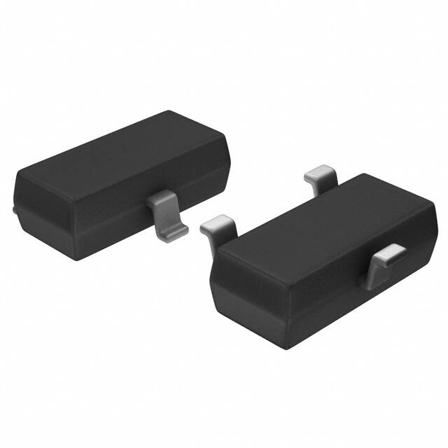
Package options for the MCP1754S include the
SOT-23A, SOT-89-3, SOT-223-3 and 2x3 DFN-8.
Package options for the MCP1754 include the
SOT-23-5, SOT-223-5 and 2x3 DFN-8.
Related Literature:
• AN765, “Using Microchip’s Micropower LDOs”
(DS00765), Microchip Technology Inc., 2007
• AN766, “Pin-Compatible CMOS Upgrades to
Bipolar LDOs” (DS00766),
Microchip Technology Inc., 2003
• AN792, “A Method to Determine How Much
Power a SOT23 Can Dissipate in an Application”
(DS00792), Microchip Technology Inc., 2001
2011-2021 Microchip Technology Inc.
DS20002276D-page 1
�MCP1754/MCP1754S
Package Types – MCP1754S
3-Pin SOT-23A
3-Pin SOT-89
VIN
GND
2
3
1
1
2
2
SOT-223-3
GND
4
VOUT 1
NC 2
1
3
VIN
VIN GND VOUT
GND VOUT
8-Lead 2x3 DFN(*)
2
NC 3
GND 4
3
8 VIN
EP
9
7 NC
6 NC
5 NC
Tab is connected to GND
GND VOUT
(Note: The 3-lead SOT-223 (DB) is
not a standard package for output
voltages below 3.0V).
* Includes Exposed Thermal Pad (EP); see Table 3-2.
Package Types – MCP1754
SOT23-5
SOT-223-5
4
5
8-Lead 2x3 DFN(*)
3
VOUT 1
PWRGD 2
1
2
3
1
2
3
4
5
NC 3
GND 4
8 VIN
EP
9
7 NC
6 NC
5 SHDN
Tab is connected to GND
PIN FUNCTION
1 VIN
2 GND
3 SHDN
4 PWRGD
5 VOUT
PIN FUNCTION
1 SHDN
2 VIN
3 GND
4 VOUT
5 PWRGD
* Includes Exposed Thermal Pad (EP); see Table 3-1.
DS20002276D-page 2
2011-2021 Microchip Technology Inc.
�MCP1754/MCP1754S
Functional Block Diagram – MCP1754S
MCP1754S
VOUT
VIN
Error Amplifier
+VIN
Voltage
Reference
+
Overcurrent
Overtemperature
GND
2011-2021 Microchip Technology Inc.
DS20002276D-page 3
�MCP1754/MCP1754S
Functional Block Diagram – MCP1754
PMOS
MCP1754
VIN
VOUT
Undervoltage
Lockout
(UVLO)
Sense
ISNS
Cf
Rf
SHDN
Overtemperature
Sensing
+
Driver w/Limit
and SHDN
EA
–
SHDN
VREF
VIN
SHDN
Reference
Soft Start
Comp
TDELAY
PWRGD
GND
92% of VREF
Typical Application Circuits
CIN
1 µF Ceramic
VIN
+
12V
MCP1754S
VOUT
GND
VOUT
5.0V
COUT
1 µF Ceramic
DS20002276D-page 4
IOUT
30 mA
2011-2021 Microchip Technology Inc.
�MCP1754/MCP1754S
1.0
ELECTRICAL
CHARACTERISTICS
† Notice: Stresses above those listed under “Maximum
Ratings” may cause permanent damage to the device. This is
a stress rating only and functional operation of the device at
those or any other conditions above those indicated in the
operational listings of this specification is not implied.
Exposure to maximum rating conditions for extended periods
may affect device reliability.
Absolute Maximum Ratings †
Input Voltage, VIN .........................................................+17.6V
VIN, PWRGD, SHDN................. (GND – 0.3V) to (VIN + 0.3V)
VOUT................................................. (GND – 0.3V) to (+5.5V)
Internal Power Dissipation .............Internally Limited (Note 6)
Output Short-Circuit Current ................................. Continuous
Storage Temperature ....................................-55°C to +150°C
Maximum Junction Temperature ...................+165°C (Note 7)
Operating Junction Temperature...................-40°C to +150°C
ESD Protection on All Pins kV HBM and 200V MM
AC/DC CHARACTERISTICS
Electrical Specifications: Unless otherwise specified, all limits are established for VIN = VR + 1V(1), ILOAD = 1 mA,
COUT = 1 µF (X7R), CIN = 1 µF (X7R), TA = +25°C, tr(VIN) = 0.5V/µs, SHDN = VIN, PWRGD = 10K to VOUT.
Boldface type applies for Junction Temperatures, TJ of -40°C to +125°C.(7)
Parameters
Sym.
Min.
Typ.
Max.
Units
Conditions
Input/Output Characteristics
Input Operating Voltage
Output Voltage Operating
Range
VIN
3.6
—
16.0
V
VOUT-RANGE
1.8
—
5.5
V
Iq
—
56
90
µA
IL = 0 mA
Input Quiescent Current for
SHDN Mode
ISHDN
—
0.1
5
µA
SHDN = GND
Ground Current
IGND
—
150
250
µA
ILOAD = 150 mA
Maximum Output Current
IOUT
150
—
—
mA
Output Soft Current Limit
IOUT_SCL
—
250
—
mA
VIN = VIN(MIN), VOUT 0.1V,
current measured 10 ms after load
is applied
Output Pulse Current Limit
IOUT_PCL
—
250
—
mA
Pulse Duration < 100 ms,
Duty Cycle < 50%, VOUT 0.1V
(Note 6)
Output Short-Circuit
Foldback Current
IOUT_SC
—
30
—
mA
VIN = VIN(MIN), VOUT = GND
Output Voltage Overshoot on
Start-up
VOVER
—
0.5
—
%VOUT
Input Quiescent Current
Output Voltage Regulation
Note 1:
2:
3:
4:
5:
6:
7:
VOUT
VR – 2.0% VR±0.2% VR + 2.0%
V
VIN = 0 to 16V, ILOAD = 150 mA
Note 2
The minimum VIN must meet two conditions: VIN3.6V and VIN VR + VDROPOUT(MAX).
VR is the nominal regulator output voltage when the input voltage, VIN = VRated + VDROPOUT(MAX) or VIN = 3.6V
(whichever is greater); IOUT = 1 mA.
TCVOUT = (VOUT-HIGH – VOUT-LOW) * 106/(VR * Temperature), VOUT-HIGH = highest voltage measured over the
temperature range. VOUT-LOW = lowest voltage measured over the temperature range.
Load regulation is measured at a constant junction temperature using low duty cycle pulse testing. Changes in output
voltage due to heating effects are determined using thermal regulation specification, TCVOUT.
Dropout voltage is defined as the input to output differential at which the output voltage drops 2% below the output
voltage value that was measured with an applied input voltage of VIN = VR + 1V or VIN = 3.6V (whichever is greater).
The maximum allowable power dissipation is a function of Ambient Temperature, the maximum allowable Junction
Temperature and the thermal resistance from Junction to Air (i.e., TA, TJ, JA). Exceeding the maximum allowable power
dissipation causes the device operating junction temperature to exceed the maximum +150°C rating. Sustained junction
temperatures above +150°C can impact the device reliability.
The junction temperature is approximated by soaking the device under test at an ambient temperature equal to the
desired junction temperature. The test time is small enough such that the rise in the junction temperature over the
ambient temperature is not significant.
2011-2021 Microchip Technology Inc.
DS20002276D-page 5
�MCP1754/MCP1754S
AC/DC CHARACTERISTICS (CONTINUED)
Electrical Specifications: Unless otherwise specified, all limits are established for VIN = VR + 1V(1), ILOAD = 1 mA,
COUT = 1 µF (X7R), CIN = 1 µF (X7R), TA = +25°C, tr(VIN) = 0.5V/µs, SHDN = VIN, PWRGD = 10K to VOUT.
Boldface type applies for Junction Temperatures, TJ of -40°C to +125°C.(7)
Parameters
Sym.
VOUT Temperature Coefficient
Min.
Typ.
Max.
Units
TCVOUT
—
22
Line Regulation
VOUT/
(VOUT x VIN)
-0.05
±0.01
Load Regulation
VOUT/VOUT
-1.1
-0.4
0
%
VDROPOUT
—
300
500
mV
IL = 150 mA
IDO
—
50
85
µA
VIN = 0.95VR, IOUT = 0 mA
Dropout Voltage (Note 5)
Dropout Current
ppm/°C
Conditions
+0.05
Note 3
VR + 1V VIN 16V
%/V
IL = 1.0 mA to 150 mA (Note 4)
Undervoltage Lockout
Undervoltage Lockout
UVLO
—
2.95
—
V
Rising VIN
Undervoltage Lockout
Hysteresis
UVLOHYS
—
285
—
mV
Falling VIN
Logic High Input
VSHDN-HIGH
2.4
—
VIN(MAX)
V
Logic Low Input
VSHDN-LOW
0.0
—
0.8
V
µA
Shutdown Input
Shutdown Input Leakage
Current
SHDNILK
—
0.100
0.500
—
0.500
2.0
SHDN = GND
SHDN = 16V
Power Good Output
PWRGD Input Voltage
Operating Range
VPWRGD_VIN
1.7
—
VIN
V
ISINK = 1 mA
PWRGD Threshold Voltage
(referenced to VOUT)
VPWRGD_TH
90
92
94
%VOUT
Falling edge of VOUT
PWRGD Threshold
Hysteresis
VPWRGD_HYS
—
2.0
—
%VOUT
Rising edge of VOUT
PWRGD Output Voltage Low
VPWRGD_L
—
0.2
0.6
V
PWRGD Output Sink Current
IPWRGD_L
5.0
—
—
mA
VPWRGD 0.4V
PWRGD Leakage Current
IPWRGD_LK
—
40
700
nA
VPWRGD pull-up = 10 k to VIN,
VIN = 16V
TPG
—
100
—
µs
Rising Edge of VOUT,
RPULLUP = 10 k
TVDET_PWRGD
—
200
—
µs
Falling edge of VOUT after
transition from
VOUT = VPRWRGD_TH + 50 mV to
VPWRGD_TH – 50 mV,
RPULLUP = 10 k to VIN
PWRGD Time Delay
Detect Threshold to PWRGD
Active Time Delay
Note 1:
2:
3:
4:
5:
6:
7:
IPWRGD_SINK = 5.0 mA, VOUT = 0V
The minimum VIN must meet two conditions: VIN3.6V and VIN VR + VDROPOUT(MAX).
VR is the nominal regulator output voltage when the input voltage, VIN = VRated + VDROPOUT(MAX) or VIN = 3.6V
(whichever is greater); IOUT = 1 mA.
TCVOUT = (VOUT-HIGH – VOUT-LOW) * 106/(VR * Temperature), VOUT-HIGH = highest voltage measured over the
temperature range. VOUT-LOW = lowest voltage measured over the temperature range.
Load regulation is measured at a constant junction temperature using low duty cycle pulse testing. Changes in output
voltage due to heating effects are determined using thermal regulation specification, TCVOUT.
Dropout voltage is defined as the input to output differential at which the output voltage drops 2% below the output
voltage value that was measured with an applied input voltage of VIN = VR + 1V or VIN = 3.6V (whichever is greater).
The maximum allowable power dissipation is a function of Ambient Temperature, the maximum allowable Junction
Temperature and the thermal resistance from Junction to Air (i.e., TA, TJ, JA). Exceeding the maximum allowable power
dissipation causes the device operating junction temperature to exceed the maximum +150°C rating. Sustained junction
temperatures above +150°C can impact the device reliability.
The junction temperature is approximated by soaking the device under test at an ambient temperature equal to the
desired junction temperature. The test time is small enough such that the rise in the junction temperature over the
ambient temperature is not significant.
DS20002276D-page 6
2011-2021 Microchip Technology Inc.
�MCP1754/MCP1754S
AC/DC CHARACTERISTICS (CONTINUED)
Electrical Specifications: Unless otherwise specified, all limits are established for VIN = VR + 1V(1), ILOAD = 1 mA,
COUT = 1 µF (X7R), CIN = 1 µF (X7R), TA = +25°C, tr(VIN) = 0.5V/µs, SHDN = VIN, PWRGD = 10K to VOUT.
Boldface type applies for Junction Temperatures, TJ of -40°C to +125°C.(7)
Parameters
Sym.
Min.
Typ.
Max.
Units
Conditions
Output Delay from VIN to
VOUT = 90% VREG
TDELAY
—
240
—
µs
VIN = 0V to 16V, VOUT = 90% VR,
tr (VIN)= 5V/µs, COUT = 1 µF,
SHDN = VIN
Output Delay from VIN to
VOUT > 0.1V
TDELAY_START
—
80
—
µs
VIN = 0V to 16V, VOUT 0.1V,
tr (VIN)= 5V/µs, COUT = 1 µF,
SHDN = VIN
Output Delay from SHDN
to VOUT = 90% VREG
TDELAY_SHDN
—
160
—
µs
VIN = 16V, VOUT = 90% VR,
COUT = 1 µF, SHDN = GND to VIN
eN
—
3
—
PSRR
—
72
—
dB
VR = 5V, f = 1 kHz, IL = 150 mA,
VINAC = 1V pk-pk, CIN = 0 µF,
VIN = VR + 1.5V
Thermal Shutdown
Temperature
TSD
—
150
—
°C
Note 6
Thermal Shutdown
Hysteresis
TSD
—
10
—
°C
AC Performance
Output Noise
Power Supply Ripple
Rejection Ratio
Note 1:
2:
3:
4:
5:
6:
7:
µV/(Hz)1/2 IL = 50 mA, f = 1 kHz,
COUT = 1 µF
The minimum VIN must meet two conditions: VIN3.6V and VIN VR + VDROPOUT(MAX).
VR is the nominal regulator output voltage when the input voltage, VIN = VRated + VDROPOUT(MAX) or VIN = 3.6V
(whichever is greater); IOUT = 1 mA.
TCVOUT = (VOUT-HIGH – VOUT-LOW) * 106/(VR * Temperature), VOUT-HIGH = highest voltage measured over the
temperature range. VOUT-LOW = lowest voltage measured over the temperature range.
Load regulation is measured at a constant junction temperature using low duty cycle pulse testing. Changes in output
voltage due to heating effects are determined using thermal regulation specification, TCVOUT.
Dropout voltage is defined as the input to output differential at which the output voltage drops 2% below the output
voltage value that was measured with an applied input voltage of VIN = VR + 1V or VIN = 3.6V (whichever is greater).
The maximum allowable power dissipation is a function of Ambient Temperature, the maximum allowable Junction
Temperature and the thermal resistance from Junction to Air (i.e., TA, TJ, JA). Exceeding the maximum allowable power
dissipation causes the device operating junction temperature to exceed the maximum +150°C rating. Sustained junction
temperatures above +150°C can impact the device reliability.
The junction temperature is approximated by soaking the device under test at an ambient temperature equal to the
desired junction temperature. The test time is small enough such that the rise in the junction temperature over the
ambient temperature is not significant.
2011-2021 Microchip Technology Inc.
DS20002276D-page 7
�MCP1754/MCP1754S
TEMPERATURE SPECIFICATIONS(1)
Parameters
Sym.
Min.
Specified Temperature Range
TA
Operating Temperature Range
TJ
Typ.
Max.
Units
-40
+125
°C
-40
+150
°C
TA
-55
+150
°C
Thermal Resistance, SOT-223-3
JA
JC
—
—
62
15
—
—
°C/W
Thermal Resistance, SOT-23A-3
JA
JC
—
—
336
110
—
—
°C/W
Thermal Resistance, SOT-89-3
JA
JC
—
—
153.3
100
—
—
°C/W
Thermal Resistance, SOT-23-5
JA
JC
—
—
256
81
—
—
°C/W
Thermal Resistance, SOT-223-5
JA
JC
—
—
62
15
—
—
°C/W
Thermal Resistance, 2X3 DFN-8
JA
JC
—
—
93
26
—
—
°C/W
Conditions
Temperature Ranges
Storage Temperature Range
Thermal Package Resistance
Note 1:
The maximum allowable power dissipation is a function of Ambient Temperature, the maximum allowable
Junction Temperature and the thermal resistance from Junction to Air (i.e., TA, TJ, JA). Exceeding the
maximum allowable power dissipation causes the device operating junction temperature to exceed the
maximum +150°C rating. Sustained junction temperatures above +150°C can impact the device reliability.
DS20002276D-page 8
2011-2021 Microchip Technology Inc.
�MCP1754/MCP1754S
2.0
TYPICAL PERFORMANCE CURVES
Note:
The graphs and tables provided following this note are a statistical summary based on a limited number of
samples and are provided for informational purposes only. The performance characteristics listed herein
are not tested or guaranteed. In some graphs or tables, the data presented may be outside the specified
operating range (e.g., outside specified power supply range) and therefore outside the warranted range.
Note 1:
Unless otherwise indicated ,VR = 3.3V, COUT = 1 µF Ceramic (X7R), CIN = 1 µF Ceramic (X7R), IL = 1 mA,
TA = +25°C, VIN = VR + 1V or VIN = 3.6V (whichever is greater), SHDN = VIN, package = SOT-223.
Junction Temperature (TJ) is approximated by soaking the device under test to an ambient temperature
equal to the desired junction temperature. The test time is small enough such that the rise in junction
temperature over the ambient temperature is not significant.
2:
180
+90°C
160
70
+25°C
+130°C
60
-45°C
0°C
50
VOUT = 1.8V
IOUT = 0 µA
GND Current (µA)
Quiescent Current (µA)
80
140
120
VOUT = 5.0V
100
80
VOUT = 3.3V
60
VOUT = 1.8V
40
40
3
4
5
6
7
8
9 10 11 12 13 14 15 16
0
20
40
Input Voltage (V)
FIGURE 2-1:
Voltage.
Quiescent Current vs. Input
FIGURE 2-4:
Current.
Quiescent Current (µA)
Quiescent Current (µA)
VOUT = 3.3V
IOUT = 0 µA
65
+130°C
+90°C
60
55
+25°C
0°C
50
-45°C
45
40
120
140
160
Ground Current vs. Load
VOUT = 5.0V
70
VOUT = 1.8V
60
50
40
30
VOUT = 3.3V
20
10
5
7
9
11
13
-45
15
-20
Input Voltage (V)
Quiescent Current vs. Input
VOUT = 5.0V
IOUT = 0 µA
+130°C
30
55
80
80
50
+25°C
30
105
130
FIGURE 2-5:
Quiescent Current vs.
Junction Temperature.
+90°C
60
40
5
Junction Temperature (°C)
0°C
-45°C
20
10
0
Quiescent Current (µA)
FIGURE 2-2:
Voltage.
Quiescent Current (µA)
100
0
3
70
80
80
70
80
60
Load Current (mA)
VOUT = 5.0V
70
60
50
+25°C
40
30
20
10
0
1.0
3.0
5.0
7.0
9.0
11.0 13.0 15.0 17.0
18
16
Input Voltage (V)
FIGURE 2-3:
Voltage.
Quiescent Current vs. Input
2011-2021 Microchip Technology Inc.
14
12
10
8
6
4
2
0
Input Voltage (V)
FIGURE 2-6:
Voltage.
Quiescent Current vs. Input
DS20002276D-page 9
�MCP1754/MCP1754S
Note 1:
2:
Unless otherwise indicated ,VR = 3.3V, COUT = 1 µF Ceramic (X7R), CIN = 1 µF Ceramic (X7R), IL = 1 mA,
TA = +25°C, VIN = VR + 1V or VIN = 3.6V (whichever is greater), SHDN = VIN, package = SOT-223.
Junction Temperature (TJ) is approximated by soaking the device under test to an ambient temperature
equal to the desired junction temperature. The test time is small enough such that the rise in junction
temperature over the ambient temperature is not significant.
1.815
1.814
+25°C
VOUT = 1.8V
1.810
1.808
+130°C
0°C
1.806
1.804
-45°C
1.802
1.800
1.810
90°C
1.805
0°C
1.800
130°C
-45°C
1.795
1.790
3
4
5
6
7
8
0
9 10 11 12 13 14 15 16
25
50
Input Voltage (V)
3.310
3.308
3.306
3.304
3.302
3.300
3.298
3.296
3.294
3.292
3.290
75
100
125
150
Load Current (mA)
Output Voltage vs. Input
FIGURE 2-10:
Current.
Output Voltage vs. Load
3.310
VOUT = 3.3V
VOUT = 3.3V
Output Voltage (V)
Output Voltage (V)
FIGURE 2-7:
Voltage.
+90°C
+130°C
+25°C
0°C
-45°C
3.305
25°C
90°C
3.300
3.295
3.290
-45°C
0°C
3.285
130°C
3.280
4
5
6
7
8
9 10 11 12 13 14 15 16
0
25
Input Voltage (V)
FIGURE 2-8:
Voltage.
50
75
100
125
150
Load Current (mA)
Output Voltage vs. Input
FIGURE 2-11:
Current.
5.020
Output Voltage vs. Load
5.020
VOUT = 5.0V
+130°C
5.012
+90°C
5.008
-45°C
VOUT = 5.0V
5.015
5.016
Output Voltage (V)
Output Voltage (V)
VOUT = 1.8V
25°C
Output Voltage (V)
Output Voltage (V)
+90°C
1.812
+25°C
5.004
130°C
5.010
90°C
5.005
5.000
25°C
4.995
4.990
4.985
0°C
5.000
6
7
-45°C
4.980
8
9
10
11
12
13
14
15
16
0
Input Voltage (V)
FIGURE 2-9:
Voltage.
DS20002276D-page 10
Output Voltage vs. Input
25
50
75
100
0°C
125
150
Load Current (mA)
FIGURE 2-12:
Current.
Output Voltage vs. Load
2011-2021 Microchip Technology Inc.
�MCP1754/MCP1754S
Note 1:
2:
Unless otherwise indicated ,VR = 3.3V, COUT = 1 µF Ceramic (X7R), CIN = 1 µF Ceramic (X7R), IL = 1 mA,
TA = +25°C, VIN = VR + 1V or VIN = 3.6V (whichever is greater), SHDN = VIN, package = SOT-223.
Junction Temperature (TJ) is approximated by soaking the device under test to an ambient temperature
equal to the desired junction temperature. The test time is small enough such that the rise in junction
temperature over the ambient temperature is not significant.
0.500
Dropout Voltage (V)
VOUT = 3.3V
0.400
+25°C
+90°C
0.300
+130°C
0.200
0°C
0.100
-45°C
0.000
0
15
30
45
60
75
90 105 120 135 150
Load Current (mA)
FIGURE 2-13:
Current.
Dropout Voltage vs. Load
FIGURE 2-16:
50
VOUT = 3.3V
0.350
+25°C
0.300
+90°C
0.250
-45°C
0.200
0.150
+130°C
0.100
0°C
0.050
0.000
Short Circuit Current (mA)
0.400
Dropout Voltage (V)
Dynamic Line Response.
0°C
25°C
90°C
130°C
40
VOUT = 3.3V
30
-45°C
20
10
0
0
15
30
45
60
75
90 105 120 135 150
4
6
Load Current (mA)
FIGURE 2-14:
Current.
Dropout Voltage vs. Load
FIGURE 2-15:
Dynamic Line Response.
2011-2021 Microchip Technology Inc.
8
10
12
14
16
Input Voltage (V)
FIGURE 2-17:
Input Voltage.
Short-Circuit Current vs.
DS20002276D-page 11
�MCP1754/MCP1754S
-0.50
-0.60
-0.70
-0.80
-0.90
-1.00
-1.10
-1.20
-1.30
-1.40
-1.50
VIN = 3.6V
VIN =
VIN = 16V
VIN = 12V
VIN = 10V
10 mA
-20
5
30
55
80
Temperature (°C)
0.00
-0.01
50 mA
150 mA
-0.02
VIN = 5V
-0.40
VIN = 16V
130
-45
VIN = 10V
VIN = 12V
-0.80
-20
5
30
55
80
Temperature (°C)
FIGURE 2-19:
Temperature.
105
Line Regulation vs.
VOUT=3.3V
0.00
10 mA
-0.01
50 mA
100 mA
150 mA
-0.02
-45
-20
5
FIGURE 2-22:
Temperature.
30
55
80
105
130
VIN = 10V
-0.60
VIN = 12V
-1.00
Line Regulation vs.
0.01
VOUT=5V
0 mA
Line Regulation (%/V)
VIN = 6V
VIN = 16V
130
Temperature (°C)
-0.20
-0.80
105
-0.03
VOUT= 5V
Iout = 1 mA to 150 mA
-0.40
30
55
80
Temperature (°C)
0 mA
130
Load Regulation vs.
0.00
5
0.01
-1.00
-45
-20
FIGURE 2-21:
Temperature.
VOUT=3.3V
Iout = 1 mA to 150 mA
VIN = 4.3V
-0.20
105
Load Regulation vs.
0.00
Load Regulation (%)
VOUT=1.8V
0 mA
100 mA
FIGURE 2-18:
Temperature.
-0.60
0.01
-0.03
-45
Load Regulation (%)
VOUT=1.8V
Iout = 1 mA to 150 mA
Line Regulation (%/V)
Load Regulation (%)
2:
Unless otherwise indicated ,VR = 3.3V, COUT = 1 µF Ceramic (X7R), CIN = 1 µF Ceramic (X7R), IL = 1 mA,
TA = +25°C, VIN = VR + 1V or VIN = 3.6V (whichever is greater), SHDN = VIN, package = SOT-223.
Junction Temperature (TJ) is approximated by soaking the device under test to an ambient temperature
equal to the desired junction temperature. The test time is small enough such that the rise in junction
temperature over the ambient temperature is not significant.
Line Regulation (%/V)
Note 1:
0.00
10 mA
-0.01
50 mA
150 mA
-0.02
100 mA
-0.03
-45
-20
5
FIGURE 2-20:
Temperature.
DS20002276D-page 12
30
55
80
Temperature (°C)
105
Load Regulation vs.
130
-45
-20
5
30
55
80
105
130
Temperature (°C)
FIGURE 2-23:
Temperature.
Line Regulation vs.
2011-2021 Microchip Technology Inc.
�MCP1754/MCP1754S
Note 1:
PSRR (dB)
2:
Unless otherwise indicated ,VR = 3.3V, COUT = 1 µF Ceramic (X7R), CIN = 1 µF Ceramic (X7R), IL = 1 mA,
TA = +25°C, VIN = VR + 1V or VIN = 3.6V (whichever is greater), SHDN = VIN, package = SOT-223.
Junction Temperature (TJ) is approximated by soaking the device under test to an ambient temperature
equal to the desired junction temperature. The test time is small enough such that the rise in junction
temperature over the ambient temperature is not significant.
0
VOUT�=�1.8V
-10
VIN�=�6.5V
-20
VINAC = 1 Vp-p
CIN�=�0 ȝF
-30
-40
-50
-60
-70
-80
-90
-100
-110
0.01
0.1
IOUT = 150 mA
IOUT = 10 mA
1
10
Frequency (NHz)
100
1000
PSRR (dB)
FIGURE 2-24:
Power Supply Ripple
Rejection vs. Frequency.
0
VOUT�=�5.0V
-10
VIN�=�6.5V
VINAC = 1V p-p
-20
CIN�=�0 ȝF
-30
-40
-50
-60
-70
-80
-90
-100
0.01
0.1
FIGURE 2-28:
Start-up from Shutdown.
IOUT = 40 mA
1
10
Frequency (NHz)
100
1000
VOUT=5.0V, VIN=6.0V
2.00
IOUT=50mA
Output Voltage (V)
10.000
1RLVH��9�¥+]�
Power-up Timing.
IOUT = 160 mA
FIGURE 2-25:
Power Supply Ripple
Rejection vs. Frequency.
1.000
0.100
FIGURE 2-27:
VOUT=3.3V, VIN=4.3V
VOUT=1.8V, VIN=3.6V
0.010
1.75
1.50
VIN = 3.6V
VOUT = 1.8V
1.25
1.00
0.75
Increasing Load
0.50
Decreasing Load
0.25
0.001
0.01
0.1
1
10
Frequency (NHz)
100
1000
FIGURE 2-26:
Output Noise vs. Frequency
(three lines, VR = 1.2V, 3.3V, 5.0V).
2011-2021 Microchip Technology Inc.
0.00
0.00
0.05
FIGURE 2-29:
Foldback.
0.10 0.15 0.20
Output Current (A)
0.25
0.30
Short-Circuit Current
DS20002276D-page 13
�MCP1754/MCP1754S
Note 1:
2:
Unless otherwise indicated ,VR = 3.3V, COUT = 1 µF Ceramic (X7R), CIN = 1 µF Ceramic (X7R), IL = 1 mA,
TA = +25°C, VIN = VR + 1V or VIN = 3.6V (whichever is greater), SHDN = VIN, package = SOT-223.
Junction Temperature (TJ) is approximated by soaking the device under test to an ambient temperature
equal to the desired junction temperature. The test time is small enough such that the rise in junction
temperature over the ambient temperature is not significant.
Output Voltage (V)
3.5
3.0
2.5
VIN = 4.3V
VOUT = 3.3V
2.0
1.5
1.0
Increasing Load
Decreasing Load
0.5
0.0
0.00
0.05
0.10 0.15 0.20
Output Current (A)
Output Voltage (V)
FIGURE 2-30:
Foldback.
5.5
5.0
4.5
4.0
3.5
3.0
2.5
2.0
1.5
1.0
0.5
0.0
0.00
0.25
0.30
Short-Circuit Current
FIGURE 2-32:
Dynamic Load Response.
FIGURE 2-33:
Dynamic Load Response.
VIN = 6V
VOUT = 5V
Increasing Load
Decreasing Load
0.05
0.10 0.15 0.20
Output Current (A)
FIGURE 2-31:
Foldback.
DS20002276D-page 14
0.25
0.30
Short-Circuit Current
2011-2021 Microchip Technology Inc.
�MCP1754/MCP1754S
3.0
PIN DESCRIPTIONS
The descriptions of the pins are listed in Table 3-1 and Table 3-2.
TABLE 3-1:
MCP1754 PIN FUNCTION TABLE
Pin No.
SOT223-5
Pin No.
SOT23-5
Pin No.
2X3 DFN
Name
4
5
1
VOUT
Function
Regulated Voltage Output
5
4
2
PWRGD
—
—
3,6,7
NC
3
2
4
GND
Ground Terminal
1
3
5
SHDN
Shutdown Input
2
1
8
VIN
EP
—
EP
GND
TABLE 3-2:
Pin No.
SOT223-3
Open-Drain Power Good Output
No Connection
Unregulated Supply Voltage
Exposed Pad, Connected to GND
MCP1754S PIN FUNCTION TABLE
Pin No.
SOT23A
Pin No.
SOT89
Pin No.
2X3 DFN
Name
3
2
3
1
VOUT
—
—
—
2,3,5,6,7
NC
2
1
2
4
GND
1
3
1
8
VIN
EP
—
EP
EP
GND
2011-2021 Microchip Technology Inc.
Function
Regulated Voltage Output
No Connection
Ground Terminal
Unregulated Supply Voltage
Exposed Pad, Connected to GND
DS20002276D-page 15
�MCP1754/MCP1754S
3.1
Regulated Output Voltage (VOUT)
Connect VOUT to the positive side of the load and the
positive terminal of the output capacitor. The positive
side of the output capacitor should be physically
located as close to the LDO VOUT pin as is practical.
The current flowing out of this pin is equal to the DC
load current.
3.2
Power Good Output (PWRGD)
The PWRGD output is an open-drain output used to
indicate when the LDO output voltage is within 92%
(typically) of its nominal regulation value. The PWRGD
threshold has a typical hysteresis value of 2%. The
PWRGD output is delayed by 100 µs (typical) from the
time the LDO output is within 92% + 2% (typical hysteresis) of the regulated output value on power-up. This
delay time is internally fixed. The PWRGD pin may be
pulled up to VIN or VOUT. Pulling up to VOUT conserves
power when the device is in Shutdown (SHDN = 0V)
mode.
3.3
Ground Terminal (GND)
Regulator ground. Tie GND to the negative side of the
output and the negative side of the input capacitor.
Only the LDO bias current flows out of this pin; there is
no high current. The LDO output regulation is referenced to this pin. Minimize the voltage drops between
this pin and the negative side of the load.
3.4
3.5
Unregulated Input Voltage (VIN)
Connect VIN to the input unregulated source voltage.
Like all Low-Dropout linear regulators, low source
impedance is necessary for the stable operation of the
LDO. The amount of capacitance required to ensure
low source impedance depends on the proximity of the
input source capacitors or battery type. For most applications, 1 µF of capacitance ensures stable operation
of the LDO circuit. The input capacitor should have a
capacitance value equal to or larger than the output
capacitor for performance applications. The input
capacitor supplies the load current during transients
and improves performance. For applications that have
load currents below 10 mA, the input capacitance
requirement can be lowered. The type of capacitor
used may be ceramic, tantalum or aluminum electrolytic. The low-ESR characteristics of the ceramic yields
better noise and PSRR performance at high frequency.
3.6
Exposed Pad (EP)
Some of the packages have an exposed metal pad on
the bottom of the package. The exposed metal pad
gives the device better thermal characteristics by
providing a good thermal path to either the PCB or heat
sink to remove heat from the device. The exposed pad
of the package is internally connected to GND.
Shutdown Input (SHDN)
The SHDN input is used to turn the LDO output voltage
on and off. When the SHDN input is at a logic high
level, the LDO output voltage is enabled. When the
SHDN input is pulled to a logic low level, the LDO
output voltage is disabled. When the SHDN input is
pulled low, the PWRGD output also goes low and the
LDO enters a Low Quiescent Current Shutdown state.
DS20002276D-page 16
2011-2021 Microchip Technology Inc.
�MCP1754/MCP1754S
4.0
DEVICE OVERVIEW
The MCP1754/MCP1754S is a 150 mA output current,
Low-Dropout (LDO) voltage regulator. The LowDropout voltage of 300 mV typical at 150 mA of current
makes it ideal for battery-powered applications. The
input voltage range is 3.6V to 16.0V. Unlike other high
output current LDOs, the MCP1754/MCP1754S
typically draws only 150 µA of quiescent current for a
150 mA load. The MCP1754 adds a shutdown control
input pin and a power good output pin. The output
voltage options are fixed.
4.1
LDO Output Voltage
The MCP1754/MCP1754S LDO has a fixed output
voltage. The output voltage range is 1.8V to 5.5V.
4.2
Output Current and Current
Limiting
The MCP1754/MCP1754S LDO is tested and ensured to
supply a minimum of 150 mA of output current. The
MCP1754/MCP1754S has no minimum output load, so
the output load current can go to 0 mA and the LDO will
continue to regulate the output voltage to within tolerance.
The MCP1754/MCP1754S also incorporates a true
output current foldback. If the output load presents an
excessive load due to a low-impedance short-circuit
condition, the output current and voltage will fold back
towards 30 mA and 0V, respectively.
The output voltage and current resume normal levels
when the excessive load is removed. If the overload
condition is a soft overload, the MCP1754/MCP1754S
supplies higher load currents of up to typically 250 mA.
This allows for device usage in applications that have
pulsed load currents having an average output current
value of 150 mA or less.
Output overload conditions may also result in an overtemperature shutdown of the device. If the junction
temperature rises above +150°C (typical), the LDO shuts
down the output. See Section 4.8 “Overtemperature
Protection” for more information on overtemperature
shutdown.
4.3
Output Capacitor
The MCP1754/MCP1754S requires a minimum output
capacitance of 1 µF for output voltage stability. Ceramic
capacitors are recommended because of their size,
cost and environmentally robust qualities.
Aluminum-electrolytic and tantalum capacitors can be
used on the LDO output as well. The Equivalent Series
Resistance (ESR) of the electrolytic output capacitor
should be no greater than 2.0. The output capacitor
should be located as close to the LDO output as is
practical. Ceramic materials, X7R and X5R, have lowtemperature coefficients and are well within the
acceptable ESR range required. A typical 1 µF X7R
0805 capacitor has an ESR of 50 milliohms.
Larger LDO output capacitors are used with the
MCP1754/MCP1754S to improve dynamic performance
and power supply ripple rejection performance. A maximum of 1000 µF is recommended. Aluminum-electrolytic
capacitors are not recommended for low-temperature
applications of 10 inches) between the input source and the LDO,
some input capacitance is recommended. A minimum
of 1.0 µF to 4.7 µF is recommended for most applications.
For applications that have output step load
requirements, the input capacitance of the LDO is very
important. The input capacitance provides the LDO
with a good local low-impedance source to pull the
transient currents from in order to respond quickly to
the output load step. For good step response
performance, the input capacitor should be of
equivalent or higher value than the output capacitor.
The capacitor should be placed as close to the input of
the LDO as is practical. Larger input capacitors also
help reduce any high-frequency noise on the input and
output of the LDO, and reduce the effects of any
inductance that exists between the input source
voltage and the input capacitance of the LDO.
4.5
The power good output is an open-drain output that can
be pulled up to any voltage equal to or less than the
LDO input voltage. This output is capable of sinking
5 mA (VPWRGD < 0.4V).
VPWRGD_TH
VOUT
TPG
VOH
TVDET_PWRGD
PWRGD
VOL
FIGURE 4-2:
Power Good Timing.
Power Good Output (PWRGD)
The open-drain PWRGD output is used to indicate when
the output voltage of the LDO is within 94% (typical value,
see Section 1.0 “Electrical Characteristics” for
minimum and maximum specifications) of its nominal
regulation value.
As the output voltage of the LDO rises, the open-drain
PWRGD output is actively held low until the output
voltage has exceeded the power good threshold plus
the hysteresis value. Once this threshold has been
exceeded, the power good time delay is started (shown
as TPG in the Electrical Characteristics table). The
power good time delay is fixed at 100 µs (typical). After
the time delay period, the PWRGD open-drain output
becomes inactive and may be pulled high by an
external pull-up resistor, indicating that the output
voltage is stable and within regulation limits. The power
good output is typically pulled up to VIN or VOUT. Pulling
the signal up to VOUT conserves power during
Shutdown mode.
VIN
TDELAY_SHDN
TPG
SHDN
VOUT
PWRGD
FIGURE 4-3:
Shutdown.
Power Good Timing from
If the output voltage of the LDO falls below the power
good threshold, the power good output will transition
low. The power good circuitry has a 200 µs delay when
detecting a falling output voltage, which helps to
increase noise immunity and avoid false triggering of
the power good output during fast output transients.
See Figure 4-2 for power good timing characteristics.
The SHDN input is an active-low input signal that turns
the LDO on and off. The SHDN threshold is a fixed
voltage level. The minimum value of this shutdown
threshold required to turn the output on is 2.4V. The
maximum value required to turn the output off is 0.8V.
When the LDO is put into Shutdown mode using the
SHDN input, the power good output is pulled low
immediately, indicating that the output voltage is out of
regulation. The timing diagram for the power good
output when using the shutdown input is shown in
Figure 4-3.
The SHDN input ignores low going pulses (pulses
meant to shut down the LDO) that are up to 400 ns in
pulse width. If the shutdown input is pulled low for more
than 400 ns, the LDO enters Shutdown mode. This
small bit of filtering helps to reject any system noise
spikes on the shutdown input signal.
DS20002276D-page 18
4.6
Shutdown Input (SHDN)
2011-2021 Microchip Technology Inc.
�MCP1754/MCP1754S
On the rising edge of the SHDN input, the shutdown
circuitry has a 70 µs delay before allowing the LDO
output to turn on. This delay helps to reject any false
turn-on signals or noise on the SHDN input signal. After
the 70 µs delay, the LDO output enters its soft start
period as it rises from 0V to its final regulation value. If
the SHDN input signal is pulled low during the 70 µs
delay period, the timer resets and the delay time starts
over again on the next rising edge of the SHDN input.
The total time from the SHDN input going high (turn-on)
to the LDO output being in regulation is typically
160 µs. See Figure 4-4 for a timing diagram of the
SHDN input.
TDELAY_SHDN
70 µs
400 ns (typical)
4.8
VOUT
4.7
For high-current applications, voltage drops across the
PCB traces must be taken into account. The trace
resistances can cause significant voltage drops
between the input voltage source and the LDO. For
applications with input voltages near 3.0V, these PCB
trace voltage drops can sometimes lower the input
voltage enough to trigger a shutdown due to
undervoltage lockout.
90 µs
SHDN
FIGURE 4-4:
Diagram.
The MCP1754/MCP1754S LDO operates across an
input voltage range of 3.6V to 16.0V and incorporates
input Undervoltage Lockout (UVLO) circuitry that keeps
the LDO output voltage off until the input voltage
reaches a minimum of 2.95V (typical) on the rising
edge of the input voltage. As the input voltage falls, the
LDO output remains on until the input voltage level
reaches 2.70V (typical).
Shutdown Input Timing
Dropout Voltage and Undervoltage
Lockout
Dropout voltage is defined as the input-to-output voltage
differential at which the output voltage drops 2% below
the nominal value that was measured with a VR + 1.0V
differential applied. The MCP1754/MCP1754S LDO has
a very Low-Dropout voltage specification of 300 mV
(typical) at 150 mA of output current. See Section 1.0
“Electrical Characteristics” for maximum dropout
voltage specifications.
2011-2021 Microchip Technology Inc.
Overtemperature Protection
The MCP1754/MCP1754S LDO has temperature
sensing circuitry to prevent the junction temperature
from exceeding approximately +150°C. If the LDO
junction temperature does reach +150°C, the LDO
output is turned off until the junction temperature cools
to approximately +137°C, at which point, the LDO output automatically resumes normal operation. If the
internal power dissipation continues to be excessive,
the device will again shut off. The junction temperature
of the die is a function of power dissipation, ambient
temperature and package thermal resistance. See
Section 5.0 “Application Circuits and Issues” for
more information on LDO power dissipation and
junction temperature.
DS20002276D-page 19
�MCP1754/MCP1754S
NOTES:
DS20002276D-page 20
2011-2021 Microchip Technology Inc.
�MCP1754/MCP1754S
5.0
APPLICATION CIRCUITS AND
ISSUES
5.1
The MCP1754/MCP1754S is most commonly used as a
voltage regulator. Its low quiescent current and LowDropout voltage make it ideal for many battery-powered
applications.
MCP1754S
GND
VIN
COUT
1 µF Ceramic
FIGURE 5-1:
5.1.1
VIN
3.6V to 4.8V
VOUT
IOUT
50 mA
T J MAX = PTOTAL R JA + T A MAX
TJ(MAX) = Maximum continuous junction
temperature
Typical Application
VOUT
1.8V
EQUATION
CIN
1 µF Ceramic
PTOTAL = Total device power dissipation
RJA = Thermal resistance from junction to
ambient
TA(MAX) = Maximum ambient temperature
The maximum power dissipation capability of a package is calculated given the junction-to-ambient thermal
resistance and the maximum ambient temperature for
the application. The following equation can be used to
determine the package maximum internal power
dissipation.
EQUATION
T J MAX – T A MAX
P D MAX = --------------------------------------------------R JA
Typical Application Circuit.
APPLICATION INPUT CONDITIONS
Package Type = SOT23
Input Voltage Range = 3.6V to 4.8V
VIN Maximum = 4.8V
VOUT Typical = 1.8V
PD(MAX) = Maximum device power dissipation
TJ(MAX) = Maximum continuous junction
temperature
TA(MAX) = Maximum ambient temperature
RJA = Thermal resistance from junction to
ambient
IOUT = 50 mA maximum
5.2
Power Calculations
5.2.1
EQUATION
T J RISE = P D MAX R JA
POWER DISSIPATION
The internal power dissipation of the MCP1754/
MCP1754S is a function of input voltage, output voltage and output current. The power dissipation, as a
result of the quiescent current draw, is so low that it is
insignificant (56.0 µA x VIN). The following equation
can be used to calculate the internal power dissipation
of the LDO.
TJ(RISE) = Rise in device junction temperature
over the ambient temperature
PD(MAX = Maximum device power dissipation
RJA = Thermal resistance from junction to
ambient
EQUATION
EQUATION
T J = T J RISE + T A
PLDO = V IN MAX – VOUT MIN IOUT MAX
PLDO = LDO pass device internal power
dissipation
TJ = Junction temperature
TJ(RISE) = Rise in device junction temperature
over the ambient temperature
TA = Ambient temperature
VIN(MAX) = Maximum input voltage
VOUT(MIN) = LDO minimum output voltage
The maximum continuous operating junction
temperature specified for the MCP1754/MCP1754S is
+150°C. To estimate the internal junction temperature
of the MCP1754/MCP1754S, the total internal power
dissipation is multiplied by the Thermal Resistance
from Junction to Ambient (RJA). The thermal resistance from junction to ambient for the SOT23A pin
package is estimated at 336°C/W.
2011-2021 Microchip Technology Inc.
5.3
Voltage Regulator
Internal power dissipation, junction temperature rise,
junction temperature and maximum power dissipation
are calculated in the following example. The power
dissipation, as a result of ground current, is small
enough to be neglected.
DS20002276D-page 21
�MCP1754/MCP1754S
5.3.1
POWER DISSIPATION EXAMPLE
Package
Package Type = SOT-23
Maximum Package Power Dissipation Examples at
+40°C Ambient Temperature
SOT-23A (336.0°C/Watt = RJA)
PD(MAX) = (125°C – 40°C)/336°C/W
Input Voltage
VIN = 3.6V to 4.8V
LDO Output Voltages and Currents
PD(MAX) = 253 milliwatts
SOT-89 (153.3°C/Watt = RJA)
PD(MAX) = (125°C – 40°C)/153.3°C/W
VOUT = 1.8V
PD(MAX) = 554 milliwatts
IOUT = 50 mA
Maximum Ambient Temperature
TA(MAX) = +40°C
Internal Power Dissipation
Internal power dissipation is the product of the LDO
output current multiplied by the voltage across the
LDO (VIN to VOUT).
PLDO(MAX) = (VIN(MAX) – VOUT(MIN)) x IOUT(MAX)
PLDO = (4.8V – (0.98 x 1.8V)) x 50 mA
PLDO = 151.8 milliwatts
5.3.1.1
Device Junction Temperature Rise
The internal junction temperature rise is a function of
internal power dissipation and the thermal resistance
from junction to ambient for the application. The
Thermal Resistance from Junction to Ambient (RJA) is
derived from an EIA/JEDEC® standard for measuring
thermal resistance for small surface-mount packages.
The EIA/JEDEC specification is JESD51-7, “High
Effective Thermal Conductivity Test Board for Leaded
Surface Mount Packages”. The standard describes the
test method and board specifications for measuring the
thermal resistance from junction to ambient. The actual
thermal resistance for a particular application can vary
depending on many factors, such as copper area and
thickness. Refer to AN792, “A Method to Determine
How Much Power a SOT23 Can Dissipate in an
Application” (DS00792) for more information regarding
this subject.
TJ(RISE) = PTOTAL x RJA
TJ(RISE) = 151.8 milliwatts x 336.0°C/Watt
TJ(RISE) = 51°C
5.3.1.2
Junction Temperature Estimate
To estimate the internal junction temperature, the
calculated temperature rise is added to the ambient or
offset temperature. For this example, the worst-case
junction temperature is estimated as follows:
TJ = TJ(RISE) + TA(MAX)
TJ = 91°C
DS20002276D-page 22
5.4
Voltage Reference
The MCP1754/MCP1754S can be used not only as a
regulator, but also as a low quiescent current voltage
reference. In many microcontroller applications, the
initial accuracy of the reference can be calibrated using
production test equipment or by using a ratio
measurement. When the initial accuracy is calibrated,
the thermal stability and line regulation tolerance are
the only errors introduced by the MCP1754/
MCP1754S LDO. The low-cost, low quiescent current
and small ceramic output capacitor are all advantages
when using the MCP1754/MCP1754S as a voltage
reference.
Ratio Metric Reference
MCP1754S
56 µA Bias
CIN
1 µF
VIN
VOUT
GND
COUT
1 µF
PIC®
Microcontroller
VREF
ADO
AD1
Bridge Sensor
FIGURE 5-2: Using the MCP1754/MCP1754S
as a Voltage Reference.
5.5
Pulsed Load Applications
For some applications, there are pulsed load current
events that may exceed the specified 150 mA
maximum specification of the MCP1754/MCP1754S.
The internal current limit of the MCP1754/MCP1754S
prevents high peak load demands from causing nonrecoverable damage. The 150 mA rating is a maximum
average continuous rating. As long as the average
current does not exceed 150 mA, pulsed higher load
currents can be applied to the MCP1754/MCP1754S.
The typical current limit for the MCP1754/MCP1754S is
250 mA (TA +25°C).
2011-2021 Microchip Technology Inc.
�MCP1754/MCP1754S
6.0
PACKAGING INFORMATION
6.1
Package Marking Information
Example:
3-Lead SOT-223 (MCP1754S only)
Part Number
XXXXXXX
XXXYYWW
NNN
Code
MCP1754S-1802E/DB
1754S18
MCP1754ST-1802E/DB
1754S18
MCP1754S-3302E/DB
1754S33
MCP1754ST-3302E/DB
1754S33
MCP1754S-5002E/DB
1754S50
MCP1754ST-5002E/DB
1754S50
3-Lead SOT-23A (MCP1754S only)
Example:
Part Number
XXNN
Code
MCP1754ST-1802E/CB
JCNN
MCP1754ST-3302E/CB
JDNN
MCP1754ST-5002E/CB
JENN
MCP1754ST-5002E/CBVAO
JENN
3-Lead SOT-89 (MCP1754S only)
Legend: XX...X
Y
YY
WW
NNN
e3
*
Note:
JC25
Example:
Part Number
NNN
1754S18
EDB1335
256
Code
MCP1754ST-1802E/MB MTYYWW
MT1335
256
MCP1754ST-3302E/MB MUYYWW
MCP1754ST-5002E/MB MVYYWW
Customer-specific information
Year code (last digit of calendar year)
Year code (last 2 digits of calendar year)
Week code (week of January 1 is week ‘01’)
Alphanumeric traceability code
Pb-free JEDEC® designator for Matte Tin (Sn)
This package is Pb-free. The Pb-free JEDEC designator ( e3 )
can be found on the outer packaging for this package.
In the event the full Microchip part number cannot be marked on one line, it will
be carried over to the next line, thus limiting the number of available characters
for customer-specific information.
2011-2021 Microchip Technology Inc.
DS20002276D-page 23
�MCP1754/MCP1754S
Package Marking Information (Continued)
Example:
5-Lead SOT-223 (2x3) (MCP1754 only)
Part Number
XXXXXXX
XXXYYWW
NNN
Code
MCP1754T-1802E/DC
175418
MCP1754T-3302E/DC
175433
MCP1754T-5002E/DC
175450
175418
EDC1335
256
Example:
5-Lead SOT-23 (2x3) (MCP1754 only)
XXNN
Part Number
Code
MCP1754T-1802E/OT
YQNN
MCP1754T-3302E/OT
YRNN
MCP1754T-5002E/OT
YSNN
MCP1754T-3302E/OTV01
YRNN
MCP1754T-3302E/OTVAO
YRNN
YQ25
Example:
8-Lead DFN (2x3) (MCP1754 only)
Part Number
DS20002276D-page 24
Code
Part Number
Code
MCP1754-1802E/MC
AKG MCP1754S-1802E/MC
ALN
MCP1754-3302E/MC
AKH MCP1754S-3302E/MC
ALM
MCP1754-5002E/MC
AKJ MCP1754S-5002E/MC
ALL
MCP1754T-1802E/MC
AKG MCP1754ST-1802E/MC
ALN
MCP1754T-3302E/MC
AKH MCP1754ST-3302E/MC
ALM
MCP1754T-5002E/MC
AKJ MCP1754ST-5002E/MC
ALL
AKJ
335
25
2011-2021 Microchip Technology Inc.
�MCP1754/MCP1754S
��/HDG�3ODVWLF�6PDOO�2XWOLQH�7UDQVLVWRU��'%��>627����@
1RWH�
)RU�WKH�PRVW�FXUUHQW�SDFNDJH�GUDZLQJV��SOHDVH�VHH�WKH�0LFURFKLS�3DFNDJLQJ�6SHFLILFDWLRQ�ORFDWHG�DW�
KWWS���ZZZ�PLFURFKLS�FRP�SDFNDJLQJ
D
b2
E1
E
3
2
1
e
e1
A2
A
b
c
φ
L
A1
8QLWV
'LPHQVLRQ�/LPLWV
1XPEHU�RI�/HDGV
0,//,0(7(56
0,1
120
0$;
1
�
/HDG�3LWFK
H
�����%6&
2XWVLGH�/HDG�3LWFK
H�
2YHUDOO�+HLJKW
$
±
±
����
6WDQGRII
$�
����
±
����
0ROGHG�3DFNDJH�+HLJKW
$�
����
����
����
2YHUDOO�:LGWK
(
����
����
����
0ROGHG�3DFNDJH�:LGWK
(�
����
����
����
2YHUDOO�/HQJWK
'
����
����
����
/HDG�7KLFNQHVV
F
����
����
����
/HDG�:LGWK
E
����
����
����
7DE�/HDG�:LGWK
E�
����
����
����
)RRW�/HQJWK
/
����
±
±
/HDG�$QJOH
�
�
±
��
�����%6&
1RWHV�
�� 'LPHQVLRQV�'�DQG�(��GR�QRW�LQFOXGH�PROG�IODVK�RU�SURWUXVLRQV��0ROG�IODVK�RU�SURWUXVLRQV�VKDOO�QRW�H[FHHG�������PP�SHU�VLGH�
�� 'LPHQVLRQLQJ�DQG�WROHUDQFLQJ�SHU�$60(�


 工商网监
湘ICP备2023018690号
工商网监
湘ICP备2023018690号
