MCP1799
80 mA High-Voltage Automotive LDO
Features
Description
• AEC-Q100 with Grade 0 and PPAP Capable
• Wide Input Voltage Range: 4.5V to 45V
- Under Voltage Lock Out: 2.8V typical
• Extended Working Temperature Range: -40°C to
+150°C
• Standard Output Regulated Voltages (VR): 3.3V
and 5.0V
- Tolerance ±2%
• Low Quiescent Supply Current: 25 µA typical
• Output Current Capability: 80 mA typical
• Stable with 1 µF Ceramic Output Capacitor
• Short Circuit Protection
• Thermal Shutdown Protection:
- +180°C typical
- Hysteresis: 22°C typical
• High PSRR:
- 70 dB @ 1 kHz typical
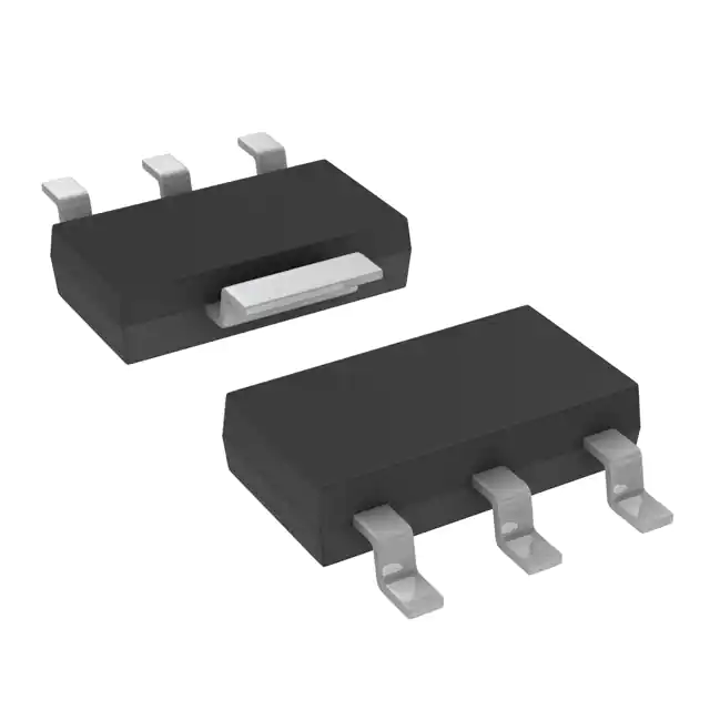
• Available in the Following Packages:
- 3-Lead SOT-23
- 3-Lead SOT-223
The MCP1799 is a high-voltage, low-dropout (LDO)
regulator, capable of generating 80 mA output current.
The input voltage range of 4.5V to 45V makes it ideal in
12V to 36V power rails and in high-voltage battery
packs.
The MCP1799 comes in two standard fixed outputvoltage versions: 3.3V and 5.0V. The regulator output
is stable with 1 µF ceramic capacitors. The device is
protected from short circuit events by the current limit
function and from over heating by means of thermal
shutdown protection.
The device itself has a low ground current of 45 µA
typical, while delivering maximum output current of 80
mA. Without load the device consumes 25 µA typical.
Applications
• Automotive Electronics
• Microcontroller Biasing
• Cordless Power Tools, Home Appliances
E-bikes, drones, etc.
• Smoke Detectors and Other Alarm Sensors
Typical Application
VBAT = 12 to 36V
1 µF
LOAD
VOUT
VIN
CIN
MCP1799
COUT
1 µF
GND
2019 Microchip Technology Inc.
DS20006248A-page 1
�MCP1799
Package Types
3-Pin SOT-23
3-Pin SOT-223
VIN
GND
4
3
1
2
GND VOUT
2019 Microchip Technology Inc.
1
VIN
2
3
GND VOUT
DS20006248A-page 2
�MCP1799
1.0
ELECTRICAL CHARACTERISTICS
Absolute Maximum Ratings †
Input Voltage ..........................................................................................................................................................+66.0V
Maximum Voltage on VIN ...................................................................................................... (GND - 0.3V) to (VIN+0.3V)
Maximum Voltage on VOUT- ............................................................................................................(GND - 0.3V) to 5.5V
Internal Power Dissipation .......................................................................... ............................Internally-Limited (Note 3)
Output Short Circuit Current..........................................................................................................................Continuous
Storage Temperature ............................................................................................................................. -55°C to +175°C
Maximum Junction Temperature, TJ ..................................................................................................................... +185°C
Operating Junction Temperature, TJ .......................................................................................................-40°C to +150°C
ESD protection on all pins:
HBM ....................................................................................................................................................................... ≥ 4 kV
CDM ...................................................................................................................................................................... ≥ 750V
MM .........................................................................................................................................................................≥ 400V
† Notice: Stresses above those listed under “Absolute Maximum Ratings” may cause permanent damage to the
device. This is a stress rating only and functional operation of the device at those or any other conditions above those
indicated in the operational listings of this specification is not intended. Exposure to maximum rating conditions for
extended periods may affect device reliability.
AC/DC CHARACTERISTICS
Electrical Specifications: Unless otherwise noted, VIN = 6.2V(for VR =5V), VIN = 4.5V(for VR =3.3V), IOUT = 1 mA,
CIN = COUT = 1.0 µF ceramic (X7R), TA = +25°C. Boldface type applies for ambient temperatures TA of -40°C to
+150°C.
Parameters
Sym.
Min.
Typ.
Max.
4.5
—
45
6.2
—
45
Units
VR = 3.3V, IOUT ≤ 80 mA
Input Operating Voltage
VIN
Input Voltage to Turn On
Output
VUVLO_High
—
2.8
—
Input Voltage to Turn Off
Output
VUVLO_Low
—
2.6
—
VOUT
VR-2%
VR
VR+2%
IQ
—
25
45
µA
IOUT = 0A
Ground Current
IGND
—
45
110
µA
IOUT = 80 mA
Maximum
Output Current
IOUT
80
—
—
mA
(Note 3)
Line Regulation
VOUT/
(VOUTxVIN)
-0.05
±0.02
+0.05
%/V
4.5V ≤ VIN ≤ 45V for VR = 3.3V
6.2V ≤ VIN ≤ 45V for VR = 5V
Input Quiescent Current
3:
4:
5:
6:
VR = 5V, IOUT ≤ 80 mA
rising VIN, VIN = 0 to VIN(MIN)
V
Output Voltage Range
Note 1:
2:
V
Conditions
falling VIN, VIN = VIN(MIN) to 0
(Note 1)
VR is the nominal regulator output voltage.
Load regulation is measured at a constant ambient temperature using a DC current source. Load
regulation is tested over a load range 1 mA to the maximum specified output current.
The maximum allowable power dissipation is a function of ambient temperature, the maximum allowable
junction temperature and the thermal resistance from junction to air. (i.e., TA, TJ, JA). See Section
“Temperature Specifications” for more information. Exceeding the maximum allowable power
dissipation will cause the device operating junction temperature to exceed the maximum +150°C rating.
Sustained junction temperatures above +150°C might impact the device reliability.
Dropout voltage is defined as the input-to-output voltage differential at which the output voltage drops 2%
below its nominal value that was measured with an input voltage of VIN = VR + 1.2V.
PSRR measurement is carried out with CIN = 0 µF, VIN = 7V, IOUT = 50 mA, VINAC = 0.4Vpkpk
Not production tested.
2019 Microchip Technology Inc.
DS20006248A-page 3
�MCP1799
AC/DC CHARACTERISTICS (CONTINUED)
Electrical Specifications: Unless otherwise noted, VIN = 6.2V(for VR =5V), VIN = 4.5V(for VR =3.3V), IOUT = 1 mA,
CIN = COUT = 1.0 µF ceramic (X7R), TA = +25°C. Boldface type applies for ambient temperatures TA of -40°C to
+150°C.
Parameters
Sym.
Min.
Typ.
Max.
Units
VOUT/VOUT
-0.8
±0.4
+0.8
%
Output Current Limit
IOUT_CL
—
150
215
mA
Output Peak Current
Limit
IOUT_PCL
1700
2500
mA
VIN = VIN(MIN), VOUT > 0.1V,
(Note 6)
mV
IOUT = 80 mA (Note 4)
Load Regulation
Dropout Voltage
VDROPOUT
—
300
1100
eN
—
500
—
Conditions
IOUT = 1 mA to 80 mA
(Note 2)
AC Performance
Output Noise
Power Supply Ripple
Rejection Ratio
Note 1:
2:
3:
4:
5:
6:
f = 100 Hz to 100 kHz
µVrms VIN = 12V, VR = 5V
IOUT = 10 mA(Note 6)
70
PSRR
—
70
35
f = 100 Hz (Note 5) (Note 6)
—
dB
f = 1 kHz (Note 5) (Note 6)
f = 100 kHz (Note 5) (Note 6)
VR is the nominal regulator output voltage.
Load regulation is measured at a constant ambient temperature using a DC current source. Load
regulation is tested over a load range 1 mA to the maximum specified output current.
The maximum allowable power dissipation is a function of ambient temperature, the maximum allowable
junction temperature and the thermal resistance from junction to air. (i.e., TA, TJ, JA). See Section
“Temperature Specifications” for more information. Exceeding the maximum allowable power
dissipation will cause the device operating junction temperature to exceed the maximum +150°C rating.
Sustained junction temperatures above +150°C might impact the device reliability.
Dropout voltage is defined as the input-to-output voltage differential at which the output voltage drops 2%
below its nominal value that was measured with an input voltage of VIN = VR + 1.2V.
PSRR measurement is carried out with CIN = 0 µF, VIN = 7V, IOUT = 50 mA, VINAC = 0.4Vpkpk
Not production tested.
2019 Microchip Technology Inc.
DS20006248A-page 4
�MCP1799
TEMPERATURE SPECIFICATIONS
Parameters
Sym.
Min.
Typ.
Max.
Units
Conditions
Temperature Ranges
Thermal Shutdown
Thermal Shutdown Hysteresis
TSD
180
°C
Rising Temperature
°C
Falling Temperature
TSD
—
22
JA
—
212
—
JC
—
139
—
JA
—
70
—
JC
—
60
—
Thermal Package Resistances
Thermal Resistance,
SOT23-3LD
Thermal Resistance,
SOT223-3LD
2019 Microchip Technology Inc.
°C/W
JEDEC® standard 4 layer FR4 board
with 1 oz. copper
DS20006248A-page 5
�MCP1799
2.0
Note:
TYPICAL PERFORMANCE CURVES
The graphs and tables provided following this note are a statistical summary based on a limited number of
samples and are provided for informational purposes only. The performance characteristics listed herein
are not tested or guaranteed. In some graphs or tables, the data presented may be outside the specified
operating range (e.g., outside specified power supply range) and therefore outside the warranted range.
Note: Unless otherwise indicated, CIN = COUT = 1 µF ceramic (X7R), IOUT = 1 mA, TA = +25°C, VIN = VR + 1.2V.
FIGURE 2-1:
Output Voltage vs. Input
Voltage (VR = 3.3V).
FIGURE 2-4:
Output Voltage vs. Output
Current (VR = 5.0V).
FIGURE 2-2:
Output Voltage vs. Input
Voltage (VR = 5.0V).
FIGURE 2-5:
Current.
0.05
Dropout Voltage vs. Output
IOUT = 1 mA to 80 mA
Load Regulation (%)
0.00
VR = 3.3V
VIN = 4.5V
-0.05
-0.10
-0.15
-0.20
-0.25
-0.30
-40
FIGURE 2-3:
Output Voltage vs. Output
Current (VR = 3.3V).
2019 Microchip Technology Inc.
-15
10
35
60
85 110
Ambient Temperature (°C)
135
160
FIGURE 2-6:
Load Regulation vs.
Ambient Temperature (VR = 3.3V).
DS20006248A-page 6
�MCP1799
Note: Unless otherwise indicated, CIN = COUT = 1 µF ceramic (X7R), IOUT = 1 mA, TA = +25°C, VIN = VR + 1.2V.
0.05
IOUT = 1 mA to 80 mA
VR = 5.0V
VIN = 6.2V
0.00
Load Regulation (%)
-0.05
-0.10
-0.15
-0.20
-0.25
-0.30
-0.35
-40
-15
10
35
60
85
110
135
160
Ambient Temperature (°C)
FIGURE 2-7:
Load Regulation vs.
Ambient Temperature (VR = 5.0V).
FIGURE 2-10:
Quiescent Current vs.Input
Voltage (VR = 3.3V).
FIGURE 2-8:
Line Regulation vs. Ambient
Temperature (VR = 3.3V).
FIGURE 2-11:
Quiescent Current vs.Input
Voltage (VR = 5.0V).
FIGURE 2-9:
Line Regulation vs. Ambient
Temperature (VR = 5.0V).
FIGURE 2-12:
Ground Current vs. Output
Current (VR = 3.3V).
2019 Microchip Technology Inc.
DS20006248A-page 7
�MCP1799
PSRR (dB)
Note: Unless otherwise indicated, CIN = COUT = 1 µF ceramic (X7R), IOUT = 1 mA, TA = +25°C, VIN = VR + 1.2V.
FIGURE 2-13:
Ground Current vs. Output
Current (VR = 5.0V).
100.000
1.000
0.100
0.010
VIN [V] = 12
VOUT [V] = 3.3
load [mA] = 10
COUT [μF] = 1
Output Noise 10 Hz - 100 kHz [μVrms] = 295.78
0.001
0.01
0.1
1
10
100
1000
10000
Frequency (kHz)
FIGURE 2-14:
(VR = 3.3V).
100
1000
FIGURE 2-16:
Power Supply Ripple
Rejection Ratio vs. Frequency (VR = 3.3V).
0
VR = 5.0V
-10
CIN = not used
COUT = 1 μF
-20
VIN = 7V + 0.4VPKPK
-30
-40
-50
-60
-70
-80
-90
-100
0.01
0.1
1
10
Frequency (kHz)
PSRR (dB)
Noise μV/√Hz
10.000
0
VR = 3.3V
-10
CIN = not used
COUT = 1 μF
-20
VIN = 7V + 0.4VPKPK
-30
-40
-50
-60
-70
-80
-90
-100
0.01
0.1
1
10
Frequency (kHz)
Noise vs. Frequency
100
1000
FIGURE 2-17:
Power Supply Ripple
Rejection Ratio vs. Frequency (VR = 5.0V).
100.000
Noise μV/√Hz
10.000
1.000
0.100
0.010
VIN [V] = 12
VOUT [V] = 5
load [mA] = 10
COUT [μF] = 1
Output Noise 10 Hz - 100 kHz [μVrms] = 444.13
0.001
0.01
0.1
1
10
100
1000
10000
Frequency (kHz)
FIGURE 2-15:
(VR = 5.0V).
Noise vs. Frequency
2019 Microchip Technology Inc.
DS20006248A-page 8
�MCP1799
Note: Unless otherwise indicated, CIN = COUT = 1 µF ceramic (X7R), IOUT = 1 mA, TA = +25°C, VIN = VR + 1.2V.
IOUT = 10 mA
VOUT
50 mV/div, BW = 20 MHz
3.3V DC Offset
VOUT
50 mV/div, BW = 20 MHz
5V DC Offset
Step from 6.2V to 14V
Step from 1 mA to 80 mA
Rise and Fall
Slope = 1V/µs
IOUT
50 mA/div
40 µs/div
FIGURE 2-18:
(VR = 3.3V).
Load Step Response
VIN
5V/div, BW = 20 MHz
6.2V DC Offset
FIGURE 2-21:
(VR = 5.0V).
40 µs/div
Line Step Response
14V
VOUT
50 mV/div, BW = 20 MHz
5V DC Offset
Rise Slope = 1V/µs
VIN
5V/div
Step from 1 mA to 80 mA
IOUT
50 mA/div
VOUT
1V/Div
200 µs/div
40 µs/div
FIGURE 2-19:
(VR = 5.0V).
IOUT = 10 mA
Load Step Response
FIGURE 2-22:
IOUT = 10 mA
Start-up (VR = 3.3V).
14V
IOUT = 10 mA
Rise Slope = 1V/µs
VOUT
50 mV/div, BW = 20 MHz
3.3V DC Offset
Step from 4.5V to 14V
VIN
5V/div
Rise and Fall
Slope = 1V/µs
VOUT
1V/Div
VIN
5V/div, BW = 20 MHz
4.5V DC Offset
FIGURE 2-20:
(VR = 3.3V).
200 µs/div
40 µs/div
Line Step Response
2019 Microchip Technology Inc.
FIGURE 2-23:
Start-up (VR = 5.0V).
DS20006248A-page 9
�MCP1799
Note: Unless otherwise indicated, CIN = COUT = 1 µF ceramic (X7R), IOUT = 1 mA, TA = +25°C, VIN = VR + 1.2V.
IOUT = 10 mA
IOUT = 10 mA
45V
45V
Rise Slope = 1V/µs
Rise Slope = 1V/µs
VIN
10V/div
VIN
10V/div
VOUT
1V/div
FIGURE 2-24:
200 µs/div
Start-up (VR = 3.3V).
2019 Microchip Technology Inc.
VOUT
1V/div
FIGURE 2-25:
200 µs/div
Start-up (VR = 5V).
DS20006248A-page 10
�MCP1799
3.0
PIN DESCRIPTION
The descriptions of the pins are listed in Table 3-1.
TABLE 3-1:
PIN FUNCTION TABLE
SOT 23-3
SOT 223-3
Symbol
1
2
GND
Ground
2
3
VOUT
Regulated Output Voltage VR
3
1
VIN
Input Voltage Supply
—
4
TAB
Exposed Thermal Pad, connected internally to GND
3.1
Ground Pin (GND)
For optimal noise and Power Supply Rejection Ratio
(PSRR) performance, the GND pin of the LDO should
be tied to an electrically “quiet” circuit ground. This will
ensure the LDO power supply rejection ratio and noise
device performance. The GND pin of the LDO conducts
only ground current, so a wide trace is not required. For
applications that have switching or noisy inputs, tie the
GND pin to the return of the output capacitor. Ground
planes help lower the inductance and as a result,
reduce the effect of fast current transients.
3.2
Description
3.3
Input Voltage Supply Pin (VIN)
Connects the voltage source to VIN. If the input voltage
source is located several inches away from the LDO, or
the input source is a battery, it is recommended that an
input capacitor be used. A typical input capacitance
value of 1 µF to 10 µF should be sufficient for most
applications. The type of capacitor used is ceramic.
However, the low ESR characteristics of the ceramic
capacitor will yield better noise and PSRR performance
at high frequency.
Regulated Output Voltage Pin
(VOUT)
The VOUT pin is the regulated output voltage VR of the
LDO. A minimum output capacitance of 1 µF is
required for the LDO to ensure the stability in all the typical applications. The MCP1799 is stable with ceramic
capacitors. See Section 4.2, Output Capacitance
Requirements for output capacitor selection guidance.
2019 Microchip Technology Inc.
DS20006248A-page 11
�MCP1799
4.0
DETAILED DESCRIPTION
4.1
Device Overview
The MCP1799 is an AEC-Q100 qualified LDO, capable
of delivering 80 mA of current, over the entire operating
temperature range. The part is stable with a minimum
1 µF output ceramic capacitor, has current limit
protection and extended working temperature range:
-40° to +150°. The device also features a PSRR of
70 dB typical for 100 Hz frequency.
FIGURE 4-1:
4.2
Simplified Functional Block Diagram.
Output Capacitance Requirements
The MCP1799 requires a minimum output capacitance
of 1 µF for output voltage stability. The output capacitor
should be located as close to the LDO output as it is
practical. The device is designed to work with low ESR
ceramic capacitors. Ceramic materials X8R\L or X7R
have low temperature coefficients and are well within
the acceptable ESR range required. A typical 1 µF X7R
0805 capacitor has an ESR of 50 m. It is
recommended to use an appropriate voltage rating
capacitor, and the derating of the capacitance as a
function of voltage and temperature needs to be taken
into account. For improved transitory behavior over the
entire temperature range, a 2.2 µF output capacitor is
recommended. The ceramic capacitor type should be
X7R or X8R/L because their dielectrics are rated for use
with temperatures between -40°C to +125° or -55°C to
+150°C, respectively.
2019 Microchip Technology Inc.
4.3
Input Capacitance Requirements
Low input-source impedance is necessary for the LDO
output to operate properly. When operating from
batteries, or in applications with long lead length
(>10 inches) between the input source and the LDO,
adding input capacitance is recommended. A minimum
of 1 µF to 10 µF of capacitance is sufficient for most
applications. Given the high input voltage capability of
the MCP1799, of up to 45V DC, it is recommended to
use an appropriate voltage rating capacitor, and the derating of the capacitance as a function of voltage and
temperature needs to be taken into account. The
ceramic capacitor type should be X7R or X8R\L
because their dielectrics are rated for use with
temperatures between -40°C to +125°C or -55°C to
+150°C, respectively.
DS20006248A-page 12
�MCP1799
4.4
Circuit Protection
The MCP1799 features current limit protection during
an output short circuit event that occurs in normal operation.
The MCP1799 was tested using the AEC-Q100 test
set-up in Figure 4-2. The testing conditions require the
use of very high parasitic inductances on the input and
output. For cases like this, it is required to prevent the
output voltage going below ground with more than 1V.
Note that the VOUT pin can withstand a maximum of
-0.3VDC (see Absolute Maximum Ratings †). This
can be achieved by placing a Schottky diode with the
cathode to VOUT and anode to ground.
Thermal shutdown functionality is present on the
device and adds to the protection features of the part.
Thermal shutdown gets triggered at typical value of
+180°C and has a typical hysteresis of 22°C.
Lshort = 5 µH
Lshort = 5 µH
VOUT
VIN
Ideal
Supply
Rshort = 10 mΩ
CIN
1 µF
ON
COUT
MCP1799
Rshort = 100 mΩ
1 µF
100V
50V
OFF
GND
GND
FIGURE 4-2:
4.5
GND
Short Circuit Test Set-Up.
Dropout Operation
4.6
Input UVLO
For VR = 5V, MCP1799 can be found operating in a
dropout condition (the minimum input voltage is 4.5V),
which can happen during a cold crank event, when the
supply voltage can drop down to 3V. It is preferred to
make sure that the part does not operate in dropout
during DC operation so that the AC performance is
maintained.
On the rising edge of the VIN input, the internal
architecture adds 550 µs delay before allowing the
regulator output to turn on. After this 550 µs delay, the
regulator starts charging the load capacitor as the
output rises from 0V to its regulated value. The
charging current amplitude will be limited by the short
circuit current value of the device.
The device has a dropout voltage of approximately
300 mV at full load and room temperature, but because
of the extended temperature range at +150°C, due to
increased leakage at hot, it reaches up to 1100 mV. For
a 5V output, the minimum supply voltage required in
order to have a regulated output, within specification, is
6.2V.
The UVLO block helps prevent false start-ups, during
the power-up sequence, until the input voltage reaches
a value of 2.8V. The minimum input voltage required for
normal operation is 4.5V.
IOUT = 10 mA
11V
VR = 5V
VIN
2V/div
4.7
Package and Device
Qualifications
The MCP1799 are AEC-Q100, grade 0 and PPAP
capable. The Grade 0 qualification allows the
MCP1799 to be used within an extended temperature
range, from -40°C to +150°C.
3V
VOUT
2V/div
FIGURE 4-3:
200 ms/div
Line Step from Dropout.
2019 Microchip Technology Inc.
DS20006248A-page 13
�MCP1799
5.0
APPLICATION INFORMATION
5.1
Typical Application
The MCP1799 is used for applications that require
high input voltage and are prone to high transient
voltages on the input.
VBAT = 4.5V to 45V
1 µF
µController
VOUT
VIN
CIN
COUT
MCP1799
1 µF
��0V DC
��V DC
GND
FIGURE 5-1:
5.2
Typical Application Circuit using a High Voltage Battery Pack.
Power Calculations
5.2.1
POWER DISSIPATION
The internal power dissipation within the MCP1799 is a
function of input voltage, output voltage, output current
and quiescent current. Equation 5-1 can be used to
calculate the internal power dissipation for the LDO.
EQUATION 5-1:
P LDO = VIN MAX – V OUT MIN I OUT MAX
Where:
PLDO = Internal power dissipation of the
LDO pass device
VIN(MAX) = Maximum input voltage
VOUT(MIN) = LDO minimum output voltage
IOUT(MAX) = Maximum output current
In addition to the LDO pass element power dissipation,
there is power dissipation within the MCP1799 as a
result of quiescent or ground current. The power
dissipation, as a result of the ground current, can be
calculated by applying Equation 5-2:
EQUATION 5-2:
PI GND = V IN MAX I GND
Where:
PI(GND) = Power dissipation due to the ground
current of the LDO
VIN(MAX) = Maximum input voltage
IGND = Current flowing into the GND pin
2019 Microchip Technology Inc.
The total power dissipated within the MCP1799 is the
sum of the power dissipated in the LDO pass device
and the P(IGND) term. Because of the CMOS
construction, the typical IGND for the MCP1799 is
typical 50 µA at full load. Operating at a maximum VIN
of 45V results in a power dissipation of 2.25 mW.
For most applications, this is small compared to the
LDO pass device power dissipation, and can be
neglected.
The maximum continuous operating junction
temperature specified for the MCP1799 is +150°C. To
estimate the internal junction temperature of the
MCP1799, the total internal power dissipation is
multiplied by the thermal resistance from junction-toambient (RJA) of the device. For example, the thermal
resistance from junction-to-ambient for the 3-Lead
SOT-223 package is estimated at 70°C/W.
EQUATION 5-3:
T J MAX = PLDO JA + T A MAX
Where:
TJ(MAX) = Maximum continuous junction
temperature
PLDO = Total power dissipation of the device
JA = Thermal resistance from junction-toambient
TA(MAX) = Maximum ambient temperature
The maximum power dissipation capability for a package can be calculated given the junction-to-ambient
thermal resistance and the maximum ambient temperature for the application. Equation 5-4 can be used
to determine the package maximum internal power
dissipation.
DS20006248A-page 14
�MCP1799
EQUATION 5-4:
P D MAX
T J MAX – T A MAX
= ---------------------------------------------------
JA
Where:
IOUT = 50 mA
Maximum Ambient Temperature
TA(MAX) = +60°C
Internal Power Dissipation
PD(MAX) = Maximum power dissipation of the
device
PLDO(MAX) = (VIN(MAX) – VOUT(MIN)) x IOUT(MAX)
PLDO = (14.7 – 4.9) x 50 mA
TJ(MAX) = Maximum continuous junction
temperature
TA(MAX) = Maximum ambient temperature
JA = Thermal resistance from
junction-to-ambient
EQUATION 5-5:
T J RISE = P D MAX JA
Where:
TJ(RISE) = Rise in the device junction
temperature over the ambient
temperature
PD(MAX) = Maximum power dissipation of the
device
JA = Thermal resistance from junction-toambient
PLDO = 0.49 Watts
5.3.1.1
Device Junction Temperature Rise
The internal junction temperature rise is a function of
internal power dissipation and of the thermal resistance
from junction-to-ambient for the application. The
thermal resistance from junction-to-ambient (JA) is
derived from EIA/JEDEC standards for measuring
thermal resistance. The EIA/JEDEC specification is
JESD51. The standard describes the test method and
board specifications for measuring the thermal
resistance from junction-to-ambient. The actual
thermal resistance for a particular application can vary
depending on many factors such as copper area and
thickness. Refer to Application Note AN792, “A Method
to Determine How Much Power a SOT23 Can
Dissipate in an Application” (DS00792), for more
information regarding this subject.
EXAMPLE 5-2:
EQUATION 5-6:
T J = T J RISE + T A
TJ = Junction temperature
TJ(RISE) = Rise in the device junction
temperature over the ambient
temperature
TA = Ambient temperature
Typical Application Examples
Internal power dissipation, junction temperature rise,
junction temperature and maximum power dissipation
are calculated in the following example. The power
dissipation as a result of ground current is small
enough to be neglected.
5.3.1
TJ(RISE) = 0.49W x 70°C/W
TJ(RISE) = 34.3°C
Where:
5.3
TJ(RISE) = PLDO(Max) x JA
POWER DISSIPATION EXAMPLE
EXAMPLE 5-1:
Package
Package Type = 3 Lead SOT223
Input Voltage
5.3.1.2
Junction Temperature Estimate
To estimate the internal junction temperature, the
calculated temperature rise is added to the ambient or
offset temperature. For this example, the worst-case
junction temperature is estimated below:
EXAMPLE 5-3:
TJ = TJ(RISE) + TA(MAX)
TJ = 34.3°C + 60.0°C
TJ = 94.3°C
5.3.1.3
Maximum Package Power
Dissipation at +60°C Ambient
Temperature
EXAMPLE 5-4:
3Lead SOT223 (JA = 70°C/W):
PD(MAX) = (150°C - 60°C)/70°C/W
PD(MAX) = 1.28W
VIN = 14V ± 5%
LDO Output Voltage and Current
VOUT = 5V
2019 Microchip Technology Inc.
DS20006248A-page 15
�MCP1799
6.0
BATTERY PACK APPLICATION
The features of the MCP1799 make it a candidate for
use in smart battery packs. The high input voltage
range of up to 45V and the transient voltage capability
makes it ideal for powering low power microcontrollers
used for monitoring battery health.
Power
Disconnect
+VBAT
Current
Sense
VBAT_1
VBAT_2
µController
MCP1799
VBAT_n-1
Network
Voltage
Sense
VBAT_n
-VBAT
FIGURE 6-1:
Smart Battery Pack Application Example.
2019 Microchip Technology Inc.
DS20006248A-page 16
�MCP1799
7.0
PACKAGING INFORMATION
7.1
Package Marking Information
3-Lead SOT-23
Example
Part Number
;;;111
Code
MCP1799T-3302H/TT
330256
MCP1799T-5002H/TT
500256
330256
3-Lead SOT-223
Example
;;;;;;;
MCP1799
3301932
256
;;;627����@
1RWH�
)RU�WKH�PRVW�FXUUHQW�SDFNDJH�GUDZLQJV��SOHDVH�VHH�WKH�0LFURFKLS�3DFNDJLQJ�6SHFLILFDWLRQ�ORFDWHG�DW�
KWWS���ZZZ�PLFURFKLS�FRP�SDFNDJLQJ
D
b2
E1
E
3
2
1
e
e1
A2
A
b
c
φ
L
A1
8QLWV
'LPHQVLRQ�/LPLWV
1XPEHU�RI�/HDGV
0,//,0(7(56
0,1
120
0$;
1
�
/HDG�3LWFK
H
�����%6&
2XWVLGH�/HDG�3LWFK
H�
2YHUDOO�+HLJKW
$
±
±
����
6WDQGRII
$�
����
±
����
0ROGHG�3DFNDJH�+HLJKW
$�
����
����
����
2YHUDOO�:LGWK
(
����
����
����
0ROGHG�3DFNDJH�:LGWK
(�
����
����
����
2YHUDOO�/HQJWK
'
����
����
����
/HDG�7KLFNQHVV
F
����
����
����
/HDG�:LGWK
E
����
����
����
7DE�/HDG�:LGWK
E�
����
����
����
)RRW�/HQJWK
/
����
±
±
/HDG�$QJOH
�
�
±
��
�����%6&
1RWHV�
�� 'LPHQVLRQV�'�DQG�(��GR�QRW�LQFOXGH�PROG�IODVK�RU�SURWUXVLRQV��0ROG�IODVK�RU�SURWUXVLRQV�VKDOO�QRW�H[FHHG�������PP�SHU�VLGH�
�� 'LPHQVLRQLQJ�DQG�WROHUDQFLQJ�SHU�$60(�