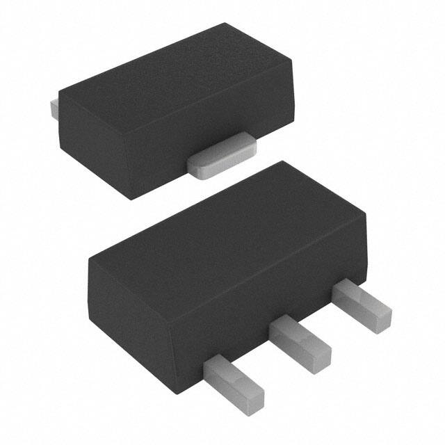
MCP1804
150 mA, 28V LDO Regulator With Shutdown
Features:
Description:
• 150 mA Output Current
• Low Dropout Voltage, 260 mV Typical @ 20 mA,
VR = 3.3V
• 50 µA Typical Quiescent Current
• 0.01 µA Typical Shutdown Current
• Input Operating Voltage Range: 2.0V to 28.0V
• Standard Output Voltage Options
(1.8V, 2.5V, 3.0V, 3.3V, 5.0V, 10.0V, 12.0V)
• Output Voltage Accuracy: ±2%
• Output Voltages from 1.8V to 18.0V in 0.1V
Increments are Available upon Request
• Stable with Ceramic Output Capacitors
• Current Limit Protection with Current Foldback
• Shutdown Pin
• High PSRR: 50 dB Typical @ 1 kHz
The MCP1804 is a family of CMOS low dropout (LDO)
voltage regulators that can deliver up to 150 mA of
current while consuming only 50 µA of quiescent
current (typical, 1.8V VOUT 5.0V). The input
operating range is specified from 2.0V to 28.0V.
Applications:
•
•
•
•
•
•
Cordless Phones, Wireless Communications
PDAs, Notebook and Netbook Computers
Digital Cameras
Microcontroller Power
Car Audio and Navigation Systems
Home Appliances
The MCP1804 is capable of delivering 100 mA with
only 1300 mV (typical) of input to output voltage
differential (VOUT = 3.3V). The output voltage tolerance
of the MCP1804 at +25°C is a maximum of ±2%. Line
regulation is ±0.15% typical at +25°C.
The LDO input and output are stable with 0.1 µF of
input and output capacitance. Ceramic, tantalum or
aluminum electrolytic capacitors can all be used for
input and output. Overcurrent limit with current foldback
to 40 mA (typical) provides short circuit protection.
A shutdown (SHDN) function allows the output to be
enabled or disabled. When disabled, the MCP1804
draws only 0.01 µA of current (typical).
Package options include the 3-lead SOT-89, 3-lead
SOT-223, 5-lead SOT-23 and 5-lead SOT-89.
Package Types
Related Literature:
• AN765, “Using Microchip’s Micropower LDOs”
(DS00765), Microchip Technology Inc., ©2002
• AN766, “Pin-Compatible CMOS Upgrades to
BiPolar LDOs” (DS00766), Microchip Technology
Inc., ©2002
• AN792, “A Method to Determine How Much
Power a SOT23 Can Dissipate in an Application”
(DS00792), Microchip Technology Inc., ©2001
SOT-89-3
SOT-223-3
(Top View)
(Top View)
1
2
3
VIN
VOUT GND
1
2
VOUT GND
3
VIN
SOT-89-5
SOT-23-5
VOUT
SHDN
VIN
NC
5
4
5
4
(Top View)
2009-2013 Microchip Technology Inc.
1
2
3
VIN
GND
NC
1
2
3
VOUT GND SHDN
DS20002200D-page 1
�MCP1804
Functional Block Diagram
VOUT
VIN
*
Thermal
Protection
SHDN
Shutdown
Control
Voltage
Reference
+
Current Limiter
Error Amplifier
*5-Pin Versions Only
GND
Typical Application Circuit
MCP1804
VIN
1
VIN VOUT
5
SOT-23
12V
Battery
+
CIN
1 µF
Ceramic
DS20002200D-page 2
2
GND
3
NC SHDN
VOUT
5.0V @ 30 mA
COUT
1 µF Ceramic
4
2009-2013 Microchip Technology Inc.
�MCP1804
1.0
ELECTRICAL
CHARACTERISTICS
Absolute Maximum Ratings †
Input Voltage ........................................................................................................................................................... +30V
Output Current (Continuous)............................................................................................................. PD/(VIN - VOUT) mA
Output Current (Peak).......................................................................................................................................... 300 mA
Output Voltage ...................................................................................................................... (VSS - 0.3V) to (VIN + 0.3V)
SHDN Voltage .................................................................................................................................. (VSS - 0.3V) to +30V
† Notice: Stresses above those listed under “Maximum
Ratings” may cause permanent damage to the device.
This is a stress rating only and functional operation of
the device at those or any other conditions above those
indicated in the operational listings of this specification
is not implied. Exposure to maximum rating conditions
for extended periods may affect device reliability.
ELECTRICAL CHARACTERISTICS
Electrical Specifications: Unless otherwise specified, all limits are established for VIN = VR + 2.0V, Note 1,
COUT = 1 µF (X7R), CIN = 1 µF (X7R), VSHDN = VIN, TA = +25°C
Parameters
Sym.
Min.
Typ.
Max.
Units
Conditions
2.0
—
28.0
V
Note 1
—
50
105
µA
1.8V VOUT 5.0V
—
60
115
µA
5.1V VOUT 12.0V
—
65
125
µA
12.1V VOUT 18.0V
—
0.01
0.10
µA
SHDN = 0V
Input / Output Characteristics
Input Operating
Voltage
VIN
Input Quiescent
Current
IQ
Shutdown Current
ISHDN
Maximum Output
Current
IOUT
Current Limiter
Output Short Circuit
Current
Output Voltage
Regulation
VOUT Temperature
Coefficient
Note 1:
2:
3:
4:
5:
—
IL = 0 mA
—
VIN = VR + 3.0V
100
—
—
mA
VOUT < 3.0V
150
—
—
mA
VOUT 3.0V
ILIMIT
—
200
—
mA
IOUT_SC
—
40
—
mA
VOUT
VR - 2.0%
VR
VR + 2.0%
V
TCVOUT
—
±100
—
ppm/°C
IOUT = 10 mA, Note 2
IOUT = 20 mA,
-40°C TA 85°C, Note 3
The minimum VIN must meet one condition: VIN (VR + 2.0V).
VR is the nominal regulator output voltage with an input voltage of VIN = VR + 2.0V.
For example: VR = 1.8V, 2.5V, 3.0V, 3.3V, etc.
TCVOUT = (VOUT-HIGH - VOUT-LOW) * 106 / (VR * Temperature), VOUT-HIGH = highest voltage measured
over the temperature range. VOUT-LOW = lowest voltage measured over the temperature range.
Load regulation is measured at a constant junction temperature using low duty cycle pulse testing.
Changes in output voltage due to heating effects are determined using thermal regulation specification
TCVOUT.
Dropout voltage is defined as the input to output differential at which the output voltage drops 2% below its
measured value with an applied input voltage of VR + 2.0V.
2009-2013 Microchip Technology Inc.
DS20002200D-page 3
�MCP1804
ELECTRICAL CHARACTERISTICS (CONTINUED)
Electrical Specifications: Unless otherwise specified, all limits are established for VIN = VR + 2.0V, Note 1,
COUT = 1 µF (X7R), CIN = 1 µF (X7R), VSHDN = VIN, TA = +25°C
Parameters
Line Regulation
Load Regulation
Dropout Voltage
Note 1, Note 5
Sym.
VOUT/(VOUTXVIN)
Min.
Typ.
Max.
Units
Conditions
(VR + 2V) VIN 28V, Note 1
—
—
0.05
0.10
%/V
IOUT = 5 mA
—
0.15
0.30
%/V
IOUT = 13 mA
—
50
90
mV
1.8V VOUT 5.0V
—
110
175
mV
5.1V VOUT 12.0V
—
180
275
mV
12.1V VOUT 18.0V
—
550
710
mV
1.8V VR 1.9V
—
450
600
mV
2.0V VR 2.1V
—
390
520
mV
2.2V VR 2.4V
—
310
450
mV
2.5V VR 2.9V
—
260
360
mV
3.0V VR 3.9V
—
220
320
mV
4.0V VR 4.9V
—
190
280
mV
5.0V VR 6.4V
—
170
230
mV
6.5V VR 8.0V
—
130
190
mV
8.1V VR 10.0V
—
120
170
mV
10.1V VR 18.0V
VOUT/VOUT
—
VDROPOUT
IL = 1.0 mA to 50 mA, Note 4
—
IL = 20 mA
—
IL = 100 mA
—
2200
2700
mV
1.8V VR 1.9V
—
1900
2600
mV
2.0V VR 2.1V
—
1700
2200
mV
2.2V VR 2.4V
—
1500
1900
mV
2.5V VR 2.9V
—
1300
1700
mV
3.0V VR 3.9V
—
1100
1500
mV
4.0V VR 4.9V
—
1000
1300
mV
5.0V VR 6.4V
—
800
1150
mV
6.5V VR 8.0V
—
700
950
mV
8.1V VR 10.0V
—
650
850
mV
10.1V VR 18.0V
SHDN “H” Voltage
VSHDN_H
1.1
—
VIN
V
VIN = 28V
SHDN “L” Voltage
VSHDN_L
0
—
0.35
V
VIN = 28V
ISHDN
-0.1
—
0.1
µA
VIN = 28V, VSHDN = GND or
VIN
SHDN Current
Note 1:
2:
3:
4:
5:
The minimum VIN must meet one condition: VIN (VR + 2.0V).
VR is the nominal regulator output voltage with an input voltage of VIN = VR + 2.0V.
For example: VR = 1.8V, 2.5V, 3.0V, 3.3V, etc.
TCVOUT = (VOUT-HIGH - VOUT-LOW) * 106 / (VR * Temperature), VOUT-HIGH = highest voltage measured
over the temperature range. VOUT-LOW = lowest voltage measured over the temperature range.
Load regulation is measured at a constant junction temperature using low duty cycle pulse testing.
Changes in output voltage due to heating effects are determined using thermal regulation specification
TCVOUT.
Dropout voltage is defined as the input to output differential at which the output voltage drops 2% below its
measured value with an applied input voltage of VR + 2.0V.
DS20002200D-page 4
2009-2013 Microchip Technology Inc.
�MCP1804
ELECTRICAL CHARACTERISTICS (CONTINUED)
Electrical Specifications: Unless otherwise specified, all limits are established for VIN = VR + 2.0V, Note 1,
COUT = 1 µF (X7R), CIN = 1 µF (X7R), VSHDN = VIN, TA = +25°C
Parameters
Sym.
Min.
Typ.
Max.
Units
PSRR
—
50
—
dB
f = 1 kHz, IL = 20 mA,
VIN_AC = 0.5V pk-pk,
CIN = 0 µF
Thermal Shutdown
Protection
TSD
—
150
—
°C
TJ = 150°C
Thermal Shutdown
Hysteresis
TSD
—
25
—
°C
Power Supply Ripple
Rejection Ratio
Note 1:
2:
3:
4:
5:
Conditions
The minimum VIN must meet one condition: VIN (VR + 2.0V).
VR is the nominal regulator output voltage with an input voltage of VIN = VR + 2.0V.
For example: VR = 1.8V, 2.5V, 3.0V, 3.3V, etc.
TCVOUT = (VOUT-HIGH - VOUT-LOW) * 106 / (VR * Temperature), VOUT-HIGH = highest voltage measured
over the temperature range. VOUT-LOW = lowest voltage measured over the temperature range.
Load regulation is measured at a constant junction temperature using low duty cycle pulse testing.
Changes in output voltage due to heating effects are determined using thermal regulation specification
TCVOUT.
Dropout voltage is defined as the input to output differential at which the output voltage drops 2% below its
measured value with an applied input voltage of VR + 2.0V.
TEMPERATURE SPECIFICATIONS
Parameters
Sym.
Min.
Typ.
Max.
Units
Operating Temperature Range
TA
-40
—
+85
°C
Operating Junction Temperature
Range
TJ
-40
—
+125
°C
Storage Temperature Range
TA
-55
—
+125
°C
JA
—
180
—
JC
—
52
—
Conditions
Temperature Ranges
Thermal Package Resistance
Thermal Resistance, 3LD SOT-89
Thermal Resistance, 3LD SOT-223
Thermal Resistance, 5LD SOT-23
Thermal Resistance, 5LD SOT-89
2009-2013 Microchip Technology Inc.
JA
—
62
—
JC
—
15
—
JA
—
256
—
JC
—
81
—
JA
—
180
—
JC
—
52
—
°C/W
EIA/JEDEC® JESD51-7
FR-4 0.063 4-Layer Board
°C/W
EIA/JEDEC JESD51-7
FR-4 0.063 4-Layer Board
°C/W
EIA/JEDEC JESD51-7
FR-4 0.063 4-Layer Board
°C/W
EIA/JEDEC JESD51-7
FR-4 0.063 4-Layer Board
DS20002200D-page 5
�MCP1804
2.0
TYPICAL PERFORMANCE CURVES
Note:
The graphs and tables provided following this note are a statistical summary based on a limited number of
samples and are provided for informational purposes only. The performance characteristics listed herein
are not tested or guaranteed. In some graphs or tables, the data presented may be outside the specified
operating range (e.g., outside specified power supply range) and therefore outside the warranted range.
TA = -40°C
TA = 25°C
TA = 85°C
VIN = SHDN = 4.8V
VR = 2.8V
0
50
100
150
200
Output Current (mA)
FIGURE 2-1:
Current.
Outtput Voltage (V)
Ou
utput Voltage (V)
2.0
1.8
2.0
1.8
1.6
1.4
1.2
1.0
0.8
06
0.6
0.4
0.2
0.0
250
Output Voltage vs. Output
1.2
1.0
0.8
06
0.6
0
5.0
3.0
2.0
VIN = SHDN = 8.0V
VR = 5V
50
100
150
200
Output Current (mA)
FIGURE 2-4:
Current.
5.0
TA = -40°C
TA = 25°C
TA = 85°C
VR = 1.8V
0.4
0.2
0.0
6.0
1.0
250
300
Output Voltage vs. Output
4.0
VIN = 6V
VIN = 7V
VIN = 8V
3.0
2.0
1.0
VR = 5.0V
0.0
0.0
0
50
100
150
200
Output Current (mA)
FIGURE 2-2:
Current.
250
0
300
Output Voltage vs. Output
14.0
12.0
12.0
10.0
TA = -40°C
TA = 25°C
TA = 85°C
6.0
4.0
VIN = SHDN = 15V
VR = 12 V
2.0
100
FIGURE 2-5:
Current.
14.0
8.0
50
150
200
250
300
Output Current (mA)
Output Voltage (V)
Outp
put Voltage (V)
1.4
6.0
4.0
VIN = 2.8V
VIN = 3.8V
VIN = 4.8V
1.6
300
Outpu
ut Voltage (V)
Output Voltage (V)
Note: Unless otherwise indicated: COUT = 1 µF Ceramic (X7R), CIN = 1 µF Ceramic (X7R), TA = +25°C,
VIN = VR + 2.0V.
Output Voltage vs. Output
10.0
VIN = 13V
VIN = 14V
VIN = 15V
8.0
6.0
4.0
2.0
0.0
VR = 12V
0.0
0
50
FIGURE 2-3:
Current.
DS20002200D-page 6
100
150
200
Output Current (mA)
250
300
Output Voltage vs. Output
0
FIGURE 2-6:
Current.
50
100
150
200
Output Current (mA)
250
300
Output Voltage vs. Output
2009-2013 Microchip Technology Inc.
�MCP1804
Note: Unless otherwise indicated: COUT = 1 µF Ceramic (X7R), CIN = 1 µF Ceramic (X7R), TA = +25°C,
VIN = VR + 2.0V.
2.1
2.1
VR = 1.8V
VR = 1.8V
2.0
IOUT = 1 mA
IOUT = 10 mA
IOUT = 30 mA
1.9
Output Voltage (V)
Outp
put Voltage (V)
2.0
1.8
1.7
1.6
1.5
1.8
1.7
IOUT = 1 mA
IOUT = 10 mA
IOUT = 30 mA
1.6
1.5
0.8
1.3
1.8
2.3
2.8
Input Voltage (V)
FIGURE 2-7:
Voltage.
3.3
3.8
Output Voltage vs. Input
4
8
FIGURE 2-10:
Voltage.
12
16
20
Input Voltage (V)
24
VR = 5V
5.8
5.6
Outp
put Voltage (V)
5.2
VR = 5V
5.8
IOUT = 1 mA
IOUT = 10 mA
IOUT = 30 mA
5.4
5.0
4.8
4.6
4.4
5.6
5.4
5.2
5.0
4.8
4.6
IOUT = 1 mA
IOUT = 10 mA
IOUT = 30 mA
4.4
4.2
4.2
4.0
4.0
4.0
4.5
FIGURE 2-8:
Voltage.
5.0
Input Voltage (V)
5.5
8
6.0
Output Voltage vs. Input
12
FIGURE 2-11:
Voltage.
15.0
16
20
Input Voltage (V)
24
28
Output Voltage vs. Input
15.0
VR = 12V
VR = 12V
14.0
Outp
put Voltage (V)
14.0
Outpu
ut Voltage (V)
28
Output Voltage vs. Input
6.0
6.0
Outp
put Voltage (V)
1.9
13.0
12.0
11 0
11.0
IOUT = 1 mA
IOUT = 10 mA
IOUT = 30 mA
10.0
13.0
12.0
11 0
11.0
IOUT = 1 mA
IOUT = 10 mA
IOUT = 30 mA
10.0
9.0
9.0
10
FIGURE 2-9:
Voltage.
11
12
Input Voltage (V)
13
14
Output Voltage vs. Input
2009-2013 Microchip Technology Inc.
14
16
FIGURE 2-12:
Voltage.
18
20
22
24
Input Voltage (V)
26
28
Output Voltage vs. Input
DS20002200D-page 7
�MCP1804
Note: Unless otherwise indicated: COUT = 1 µF Ceramic (X7R), CIN = 1 µF Ceramic (X7R), TA = +25°C,
VIN = VR + 2.0V.
70
4.0
Sup
pply Current (µA)
Dropo
out Voltage (V)
3.5
TA = 85°C
TA = 25°C
TA = -40°C
3.0
2.5
2.0
1.5
1.0
60
50
40
30
TA = 85°C
8 °C
TA = 25°C
TA = -40°C
20
10
0.5
0
0.0
0
25
50
75
100
Output Current (mA)
FIGURE 2-13:
Current.
125
0
150
Dropout Voltage vs. Load
TA = 85°C
TA = 25°C
TA = -40°C
2.5
2.0
1.5
1.0
12
16
20
Input Voltage (V)
28
Supply Current vs. Input
60
50
40
30
TA = 85°C
TA = 25°C
TA = -40°C
20
10
0.5
0.0
0
0
25
FIGURE 2-14:
Current.
50
75
100
Output Current (mA)
125
150
Dropout Voltage vs. Load
0
4
8
FIGURE 2-17:
Voltage.
4.0
12
16
20
Input Voltage (V)
24
28
Supply Current vs. Input
70
VR = 12V
3.0
TA = 85°C
TA = 25°C
TA = -40°C
2.5
2.0
VR = 12V
Sup
pply Current (µA)
3.5
Dropout Voltage (V)
24
VR = 5V
Sup
pply Current (µA)
3.0
8
70
VR = 5V
3.5
4
FIGURE 2-16:
Voltage.
4.0
Drop
pout Voltage (V)
VR = 1.8V
VR = 1.8V
1.5
1.0
60
50
40
30
TA = 85°C
TA = 25°C
TA = -40°C
20
10
0.5
0
0.0
0
25
FIGURE 2-15:
Current.
DS20002200D-page 8
50
75
100
Output Current (mA)
125
150
Dropout Voltage vs. Load
0
4
FIGURE 2-18:
Voltage.
8
12
16
20
Input Voltage (V)
24
28
Supply Current vs. Input
2009-2013 Microchip Technology Inc.
�MCP1804
Note: Unless otherwise indicated: COUT = 1 µF Ceramic (X7R), CIN = 1 µF Ceramic (X7R), TA = +25°C,
VIN = VR + 2.0V.
2.00
70
VR = 1.8V
1.95
60
Outtput Voltage (V)
Sup
pply Current (µA)
VR = 1.8V
50
40
30
20
10
1.80
1.75
IOUT = 1 mA
IOUT = 10 mA
IOUT = 20 mA
1.70
1.60
-40
-20
FIGURE 2-19:
Voltage.
0
20
40
60
Ambient Temperature (°C)
80
100
Supply Current vs. Input
-50
-25
0
25
50
75
Ambient Temperature (°C㸧
FIGURE 2-22:
Temperature.
70
40
30
20
VR = 5V
5.15
Ou
utput Voltage (V)
50
100
Output Voltage vs. Ambient
5.20
VR = 5V
60
Sup
pply Current (µA)
1.85
1.65
0
10
5.10
5.05
5.00
4.95
IOUT = 1 mA
IOUT = 10 mA
IOUT = 20 mA
4.90
4.85
4.80
0
-40
-20
FIGURE 2-20:
Voltage.
0
20
40
60
Ambient Temperature (°C)
80
-50
100
Supply Current vs. Input
30
20
Output Voltage vs. Ambient
VR = 12V
12.4
Output Voltage (V)
40
12.3
12.2
12.1
12.0
11.9
11.8
IOUT = 1 mA
IOUT = 10 mA
IOUT = 20 mA
11.7
10
11.6
0
100
12.5
VR = 12V
60
50
-25
0
25
50
75
Ambient Temperature (°C㸧
FIGURE 2-23:
Temperature.
70
Sup
pply Current (µA)
1.90
11.5
-40
-20
FIGURE 2-21:
Voltage.
0
20
40
60
Ambient Temperature (°C)
80
100
Supply Current vs. Input
2009-2013 Microchip Technology Inc.
-50
FIGURE 2-24:
Temperature.
-25
0
25
50
75
Ambient Temperature (°C㸧
100
Output Voltage vs. Ambient
DS20002200D-page 9
�MCP1804
Note: Unless otherwise indicated: COUT = 1 µF Ceramic (X7R), CIN = 1 µF Ceramic (X7R), TA = +25°C,
VIN = VR + 2.0V.
3.34
4.3
3.32
VOUT
3.3
3.30
2.3
Time (1 ms/div)
Inpu
ut Voltage (V)
8
VIN
7
4.3
3.26
1.3
3.26
FIGURE 2-28:
9
7
4
4.98
4.96
3
FIGURE 2-29:
Dynamic Line Response.
16
12.08
VIN
12.06
14
12.04
12.02
VOUT
15
put Voltage (V)
Inp
VR = 12V
IOUT = 1 mA
Outp
put Voltage (V)
Inpu
ut Voltage (V)
4.96
Time (1 ms/div)
15
14
VR = 12V
IOUT = 30 mA
12.08
12.06
12.04
13
12.02
VOUT
12
12.00
11.98
11
11.98
11.96
10
12
12.00
11
Dynamic Line Response.
11.96
Time (1 ms/div)
Time (1 ms/div)
DS20002200D-page 10
5.02
VOUT
4.98
Dynamic Line Response.
FIGURE 2-27:
5.04
6
Time (1 ms/div)
10
5.06
5.00
4
13
VR = 5V
IOUT = 30 mA
5
5.00
VIN
5.08
8
5.06
5
16
Dynamic Line Response.
VIN
5.02
FIGURE 2-26:
3.32
VOUT
3.28
VOUT
3
3.34
2.3
5.04
6
5.3
3.28
5.08
VR = 5V
IOUT = 1 mA
3.36
3.30
Dynamic Line Response.
9
6.3
Output Voltage (V)
FIGURE 2-25:
3.38
3.3
Inp
put Voltage (V)
1.3
VR = 3.3V
IOUT = 30 mA
Outp
put Voltage (V)
5.3
3.36
Inpu
ut Voltage (V)
VIN
VIN
Outp
put Voltage (V)
Input Voltage (V)
6.3
7.3
Outtput Voltage (V)
3.38
VR = 3.3V
IOUT = 1 mA
Outp
put Voltage (V)
7.3
FIGURE 2-30:
Dynamic Line Response.
2009-2013 Microchip Technology Inc.
�MCP1804
Note: Unless otherwise indicated: COUT = 1 µF Ceramic (X7R), CIN = 1 µF Ceramic (X7R), TA = +25°C,
VIN = VR + 2.0V.
3.3
3.2
90
3.1
3.0
6
2
5
0
-2
0
Dynamic Load Response.
5.2
120
5.1
VOUT
90
4.9
4.8
60
IOUT
4.6
Inp
put Voltage (V)
6
4.7
30
0
2
0
5
VOUT
-2
FIGURE 2-35:
150
3
VR = 3.3V
IOUT = 30 mA
11.4
60
IOUT
11.0
30
Input Voltage (V)
11.6
Outpu
ut Current (mA)
120
90
11.8
0
8
7
VIN
4
2
6
Dynamic Load Response.
5
VOUT
0
4
2
-2
3
-4
VR = 5.0V
IOUT = 1 mA
-8
2
1
0
Time (1 ms/div)
Time (1 ms/div)
2009-2013 Microchip Technology Inc.
1
Start-up Response.
-6
10.8
10.6
2
0
8
6
VOUT
4
Time (1 ms/div)
VR = 12V
12.4
Outp
put Voltage (V)
6
-8
Dynamic Load Response.
12.6
FIGURE 2-33:
7
4
Time (1 ms/div)
11.2
8
VIN
-6
4.4
12.0
Start-up Response.
-4
4.5
12.2
0
8
150
Outpu
ut Current (mA)
Outp
put Voltage (V)
FIGURE 2-34:
VR = 5V
5.3
1
Time (1 ms/div)
5.4
FIGURE 2-32:
2
VR = 3.3V
IOUT = 1 mA
-8
Time (1 ms/div)
5.0
3
-6
2.6
4
VOUT
-4
30
2.7
FIGURE 2-31:
7
4
Outp
put Voltage (V)
2.8
IOUT
8
VIN
Outp
put Voltage (V)
2.9
60
Inp
put Voltage (V)
6
120
VOUT
Output Current (mA)
put Voltage (V)
Outp
3.4
8
150
VR = 3.3V
3.5
Outp
put Voltage (V)
3.6
FIGURE 2-36:
Start-up Response.
DS20002200D-page 11
�MCP1804
Note: Unless otherwise indicated: COUT = 1 µF Ceramic (X7R), CIN = 1 µF Ceramic (X7R), TA = +25°C,
VIN = VR + 2.0V.
6
4
6
2
5
VOUT
0
4
2
-2
3
2
VR = 5.0V
IOUT = 30 mA
-6
-8
4
6
2
5
0
-2
FIGURE 2-40:
18
VOUT
0
9
-5
6
VR = 12V
IOUT = 1 mA
SHD
DN Voltage (V)
12
-10
6
15
5
2
0
4
2
-2
3
2
VR = 5V
IOUT = 1 mA
1
0
SHDN Response.
15
18
SHDN
15
12
VOUT
0
9
-5
6
VR = 12V
IOUT = 30 mA
-15
SHD
DN Voltage (V)
5
10
Outp
put Voltage (V)
Inp
put Voltage (V)
FIGURE 2-41:
18
VIN
Start-up Response.
15
5
12
VOUT
0
9
-5
6
3
-10
0
-15
VR = 12V
IOUT = 1 mA
3
0
Time (1 ms/div)
Time (1 ms/div)
DS20002200D-page 12
5
VOUT
Time (1 ms/div)
15
FIGURE 2-39:
6
-8
Start-up Response.
-10
7
4
Time (1 ms/div)
10
8
SHDN
-6
0
FIGURE 2-38:
SHDN Response.
-4
3
-15
0
8
Outp
put Voltage (V)
Inp
put Voltage (V)
10
1
Time (1 ms/div)
Start-up Response.
VIN
2
VR = 3.3V
IOUT = 1 mA
-8
0
15
3
-4
Time (1 ms/div)
FIGURE 2-37:
4
VOUT
-6
1
7
Outpu
ut Voltage (V)
-4
8
SHDN
Outpu
ut Voltage (V)
8
7
Outpu
ut Voltage (V)
VIN
SHDN
N Voltage (V)
Inp
put Voltage (V)
6
8
Outp
put Voltage (V)
8
FIGURE 2-42:
SHDN Response.
2009-2013 Microchip Technology Inc.
�MCP1804
Note: Unless otherwise indicated: COUT = 1 µF Ceramic (X7R), CIN = 1 µF Ceramic (X7R), TA = +25°C,
VIN = VR + 2.0V.
SHD
DN Voltage (V)
6
8
90
7
80
4
6
2
5
VOUT
0
4
2
-2
3
-4
2
VR = 3.3V
IOUT = 30 mA
-6
-8
VOUT = 3.3V
CIN = 0
IOUT = 1 mA
VIN_AC = 0.5Vpk-pk
70
PSRR (dB)
SHDN
Outpu
ut Voltage (V)
8
60
50
40
30
20
10
1
0
0.01
0
0.1
Time (1 ms/div)
8
4
6
2
5
VOUT
0
4
2
-2
3
-4
2
VR = 5V
IOUT = 30 mA
-6
-8
VOUT = 5V
CIN = 0
IOUT = 1 mA
VIN_AC = 0.5Vpk-pk
70
60
50
40
30
20
10
1
0
0.01
0
0.1
Time (1 ms/div)
FIGURE 2-44:
FIGURE 2-47:
SHDN Response.
15
18
5
12
VOUT
0
9
-5
6
VR = 12V
IOUT = 30 mA
-15
3
0
SHDN Response.
2009-2013 Microchip Technology Inc.
100
VOUT = 12V
CIN = 0
IOUT = 1 mA
VIN_AC = 0.5Vpk-pk
70
60
50
40
30
20
10
0
0.01
Time (1 ms/div)
FIGURE 2-45:
10
PSRR 5.0V @ 1 mA.
80
PSRR (dB)
P
15
Outpu
ut Voltage (V)
SHD
DN Voltage (V)
10
1
Frequency (kHz)
90
SHDN
-10
100
PSRR 3.3V @ 1 mA.
80
7
SHDN
10
90
8
PSRR (dB)
SHD
DN Voltage (V)
6
FIGURE 2-46:
SHDN Response.
Outp
put Voltage (V)
FIGURE 2-43:
1
Frequency (kHz)
FIGURE 2-48:
0.1
1
Frequency (kHz)
10
100
PSRR 12.0V @ 1 mA.
DS20002200D-page 13
�MCP1804
Note: Unless otherwise indicated: COUT = 1 µF Ceramic (X7R), CIN = 1 µF Ceramic (X7R), TA = +25°C,
VIN = VR + 2.0V.
80
90
80
70
PS
SRR (dB)
60
50
40
30
20
VOUT = 5V
VIN = 8V
70
Groun
nd Current (µA)
VOUT = 3.3V
CIN = 0
IOUT = 30 mA
VIN_AC = 0.5Vpk-pk
60
50
40
30
10
0
0.01
20
0.1
1
Frequency (kHz)
FIGURE 2-49:
10
0
100
PSRR 3.3V @ 30 mA.
FIGURE 2-52:
Current.
50
75
100
Output Current (mA)
125
150
Ground Current vs. Output
80
VOUT = 5V
CIN = 0
IOUT = 30 mA
VIN_AC = 0.5Vpk-pk
80
70
60
50
40
30
20
Grou
und Current (µA)
90
PSRR (dB)
P
25
VOUT = 12V
VIN = 15V
70
60
50
40
30
10
0
0.01
20
0.1
FIGURE 2-50:
1
Frequency (kHz)
10
0
100
FIGURE 2-53:
Current.
PSRR 5.0V @ 30 mA.
50
75
100
Output Current (mA)
125
150
Ground Current vs. Output
100
90
VOUT = 12V
CIN = 0
IOUT = 30 mA
VIN_AC = 0.5Vp-p
70
VOUT = 15V
VIN = 18V
90
Groun
nd Current (µA)
80
PSRR (dB)
25
60
50
40
30
20
80
70
60
50
40
10
0
0.01
30
0.1
FIGURE 2-51:
DS20002200D-page 14
1
Frequency (kHz)
10
PSRR 12V @ 30 mA.
100
0
25
50
75
100
125
150
Output Current (mA)
FIGURE 2-54:
Current.
Ground Current vs. Output
2009-2013 Microchip Technology Inc.
�MCP1804
Note: Unless otherwise indicated: COUT = 1 µF Ceramic (X7R), CIN = 1 µF Ceramic (X7R), TA = +25°C,
VIN = VR + 2.0V.
Output Noise (µV/Hz)
10.00
VR = 3.3V
VIN = 5.0V
IOUT = 50 mA
1.00
0.10
0.01
0.01
FIGURE 2-55:
0.1
1
Frequency (kHz)
10
100
Output Noise vs. Frequency.
2009-2013 Microchip Technology Inc.
DS20002200D-page 15
�MCP1804
3.0
PIN DESCRIPTIONS
The descriptions of the pins are listed in Table 3-1.
.
TABLE 3-1:
MCP1804 PIN FUNCTION TABLE
MCP1804
SOT-23-5
3.1
SOT-89-5
SOT-89-3
Symbol
SOT-223-3
1
5
3
3
VIN
2
2, TAB
2, TAB
2, TAB
GND
Description
Unregulated Supply Voltage
Ground Terminal
3
4
—
—
NC
4
3
—
—
SHDN
Shutdown
5
1
1
1
VOUT
Regulated Voltage Output
Unregulated Input Voltage (VIN)
3.4
No connection
Regulated Output Voltage (VOUT)
Connect VIN to the input unregulated source voltage.
Like all low dropout linear regulators, low source
impedance is necessary for the stable operation of the
LDO. The amount of capacitance required to ensure
low source impedance will depend on the proximity of
the input source capacitors or battery type. For most
applications, 0.1 µF to 1.0 µF of capacitance will
ensure stable operation of the LDO circuit. The type of
capacitor used can be ceramic, tantalum or aluminum
electrolytic. The low ESR characteristics of the ceramic
will yield better noise and PSRR performance at high
frequency.
Connect VOUT to the positive side of the load and the
positive terminal of the output capacitor. The positive
side of the output capacitor should be physically
located as close to the LDO VOUT pin as is practical.
The current flowing out of this pin is equal to the DC
load current. For most applications, 0.1 µF to 1.0 µF of
capacitance will ensure stable operation of the LDO
circuit. Larger values may be used to improve dynamic
load response. The type of capacitor used can be
ceramic, tantalum or aluminum electrolytic. The low
ESR characteristics of the ceramic will yield better
noise and PSRR performance at high frequency.
3.2
3.5
Ground Terminal (GND)
Regulator ground. Tie GND to the negative side of the
output and the negative side of the input capacitor.
Only the LDO bias current (50 to 60 µA typical) flows
out of this pin; there is no high current. The LDO output
regulation is referenced to this pin. Minimize voltage
drops between this pin and the negative side of the
load.
3.3
No Connect (NC)
No internal connection. The pins marked NC are true
“No Connect” pins.
Shutdown Input (SHDN)
The SHDN input is used to turn the LDO output voltage
on and off. When the SHDN input is at a logic-high
level, the LDO output voltage is enabled. When the
SHDN input is pulled to a logic-low level, the LDO
output voltage is disabled and the LDO enters a low
quiescent current shutdown state where the typical
quiescent current is 0.01 µA. The SHDN pin does not
have an internal pull-up or pull-down resistor. The
SHDN pin must be connected to either VIN or GND to
prevent the device from becoming unstable.
DS20002200D-page 16
2009-2013 Microchip Technology Inc.
�MCP1804
4.0
DETAILED DESCRIPTION
4.1
Output Regulation
A portion of the LDO output voltage is fed back to the
internal error amplifier and compared with the precision
internal bandgap reference. The error amplifier output
will adjust the amount of current that flows through the
P-Channel pass transistor, thus regulating the output
voltage to the desired value. Any changes in input
voltage or output current will cause the error amplifier
to respond and adjust the output voltage to the target
voltage (refer to Figure 4-1).
4.2
Overcurrent
The MCP1804 internal circuitry monitors the amount of
current flowing through the P-Channel pass transistor.
In the event that the load current reaches the current
limiter level of 200 mA (typical), the current limiter
circuit will operate and the output voltage will drop. As
the output voltage drops, the internal current foldback
circuit will further reduce the output voltage causing the
output current to decrease. When the output is shorted,
a typical output current of 50 mA flows.
4.3
Shutdown
The SHDN input is used to turn the LDO output voltage
on and off. When the SHDN input is at a logic-high
level, the LDO output voltage is enabled. When the
SHDN input is pulled to a logic-low level, the LDO
output voltage is disabled and the LDO enters a low
quiescent current shutdown state where the typical
quiescent current is 0.01 µA. The SHDN pin does not
have an internal pull-up or pull-down resistor. Therefore
the SHDN pin must be pulled either high or low to
prevent the device from becoming unstable. The
internal device current will increase when the device is
operational and current flows through the pull-up or
pull-down resistor to the SHDN pin internal logic. The
SHDN pin internal logic is equivalent to an inverter
input.
4.4
Output Capacitor
The MCP1804 requires a minimum output capacitance
of 0.1 µF to 1.0 µF for output voltage stability. Ceramic
capacitors are recommended because of their size,
cost and environmental robustness qualities.
Aluminum-electrolytic and tantalum capacitors can be
used on the LDO output as well. The output capacitor
should be located as close to the LDO output as is
practical. Ceramic materials X7R and X5R have low
temperature coefficients.
Larger LDO output capacitors can be used with the
MCP1804 to improve dynamic performance and power
supply ripple rejection performance. Aluminumelectrolytic capacitors are not recommended for low
temperature applications of < -25°C.
4.5
Input Capacitor
Low input source impedance is necessary for the LDO
output to operate properly. When operating from
batteries or in applications with long lead length
(> 10 inches) between the input source and the LDO,
some input capacitance is recommended. A minimum
of 0.1 µF to 1.0 µF is recommended for most
applications.
For applications that have output step load
requirements, the input capacitance of the LDO is very
important. The input capacitance provides the LDO
with a good local low-impedance source to pull the
transient currents from in order to respond quickly to
the output load step. For good step response
performance, the input capacitor should be of
equivalent or higher value than the output capacitor.
The capacitor should be placed as close to the input of
the LDO as is practical. Larger input capacitors will also
help reduce any high-frequency noise on the input and
output of the LDO and reduce the effects of any
inductance that exists between the input source
voltage and the input capacitance of the LDO.
4.6
Thermal Shutdown
The MCP1804 thermal shutdown circuitry protects the
device when the internal junction temperature reaches
the typical thermal limit value of +150°C. The thermal
limit shuts off the output drive transistor. Device output
will resume when the internal junction temperature falls
below the thermal limit value by an amount equal to the
thermal limit hysteresis value of +25°C.
2009-2013 Microchip Technology Inc.
DS20002200D-page 17
�MCP1804
VOUT
VIN
*
Thermal
Protection
SHDN
Shutdown
Control
Voltage
Reference
+
Current Limiter
Error Amplifier
*5-Pin Versions Only
FIGURE 4-1:
DS20002200D-page 18
GND
Block Diagram.
2009-2013 Microchip Technology Inc.
�MCP1804
5.0
FUNCTIONAL DESCRIPTION
The MCP1804 CMOS linear regulator is intended for
applications that need low current consumption while
maintaining output voltage regulation. The operating
continuous load of the MCP1804 ranges from 0 mA to
150 mA. The input operating voltage ranges from 2.0V
to 28.0V, making it capable of operating from a single
12V battery or single and multiple Li-Ion cell batteries.
5.1
Input
The input of the MCP1804 is connected to the source
of the P-Channel PMOS pass transistor. As with all
LDO circuits, a relatively low source impedance
(< 10) is needed to prevent the input impedance from
causing the LDO to become unstable. The size and
type of the capacitor needed depend heavily on the
input source type (battery, power supply) and the
output current range of the application. For most
applications, a 0.1 µF ceramic capacitor will be
sufficient to ensure circuit stability. Larger values can
be used to improve circuit AC performance.
5.2
Output
The maximum rated continuous output current for the
MCP1804 is 150 mA.
A minimum output capacitance of 0.1 µF to 1.0 µF is
required for small signal stability in applications that
have up to 150 mA output current capability. The
capacitor type can be ceramic, tantalum or aluminum
electrolytic.
2009-2013 Microchip Technology Inc.
DS20002200D-page 19
�MCP1804
NOTES:
DS20002200D-page 20
2009-2013 Microchip Technology Inc.
�MCP1804
6.0
APPLICATION CIRCUITS AND
ISSUES
6.1
The MCP1804 is most commonly used as a voltage
regulator. Its low quiescent current and wide input
voltage make it ideal for Li-Ion and 12V batterypowered applications.
VOUT
IOUT
50 mA
NC
GND
VIN
COUT
1 µF Ceramic
FIGURE 6-1:
6.1.1
MCP1804
VOUT
1.8V
VIN
4.2V
CIN
1 µF
Ceramic
TJ(MAX)
=
Maximum continuous junction
temperature
PTOTAL
=
Total power dissipation of the device
RJA
=
Thermal resistance from junction to
ambient
TA(MAX)
=
Maximum ambient temperature
The maximum power dissipation capability for a
package can be calculated given the junctionto-ambient thermal resistance and the maximum
ambient temperature for the application. The following
equation can be used to determine the package
maximum internal power dissipation.
EQUATION 6-3:
T J MAX – T A MAX
P D MAX = --------------------------------------------------R JA
Typical Application Circuit.
APPLICATION INPUT CONDITIONS
Package Type
= SOT-23
Input Voltage Range
= 3.8V to 4.2V
VIN maximum
= 4.6V
VOUT typical
= 1.8V
IOUT
= 50 mA maximum
6.2
T J MAX = PTOTAL R JA + T A MAX
Where:
Typical Application
SHDN
EQUATION 6-2:
Where:
PD(MAX)
=
Maximum power dissipation of the
device
TJ(MAX)
=
Maximum continuous junction
temperature
TA(MAX)
=
Maximum ambient temperature
RJA
=
Thermal resistance from junction to
ambient
Power Calculations
6.2.1
POWER DISSIPATION
The internal power dissipation of the MCP1804 is a
function of input voltage, output voltage and output
current. The power dissipation resulting from the
quiescent current draw is so low it is insignificant
(50.0 µA x VIN). The following equation can be used to
calculate the internal power dissipation of the LDO.
EQUATION 6-1:
P LDO = VIN MAX – V OUT MIN I OUT
Where:
PLDO = Internal power dissipation of the LDO
Pass device
VIN(MAX) = Maximum input voltage
VOUT(MIN) = Minimum output voltage of the LDO
The maximum continuous operating temperature
specified for the MCP1804 is +85°C. To estimate the
internal junction temperature of the MCP1804, the total
internal power dissipation is multiplied by the thermal
resistance from junction to ambient (RJA). The thermal
resistance from junction to ambient for the SOT-23 pin
package is estimated at 256°C/W.
2009-2013 Microchip Technology Inc.
EQUATION 6-4:
T J RISE = P D MAX R JA
Where:
TJ(RISE)
=
Rise in the device’s junction
temperature over the ambient
temperature
PD(MAX)
=
Maximum power dissipation of the
device
RJA
=
Thermal resistance from junction to
ambient
EQUATION 6-5:
T J = T J RISE + T A
Where:
TJ
=
Junction Temperature
TJ(RISE)
=
Rise in the device’s junction
temperature over the ambient
temperature
TA
=
Ambient temperature
DS20002200D-page 21
�MCP1804
6.3
Voltage Regulator
Internal power dissipation, junction temperature rise,
junction temperature and maximum power dissipation
are calculated in the following example. The power
dissipation resulting from ground current is small
enough to be neglected.
6.3.1
POWER DISSIPATION EXAMPLE
TJ = TJ(RISE) + TA(MAX)
TJ = 76.3°C
Maximum Package Power Dissipation at +25°C
Ambient Temperature (minimum PCB footprint)
SOT-23 (256°C/Watt = RJA):
PD(MAX) = (125°C - 25°C) / 256°C/W
Package:
Package Type = SOT-23
Input Voltage:
PD(MAX) = 390 milli-Watts
SOT-89 (180°C/Watt = RJA):
PD(MAX) = (125°C - 25°C) / 180°C/W
VIN = 3.8V to 4.6V
PD(MAX) = 555 milli-Watts
LDO Output Voltages and Currents:
VOUT = 1.8V
IOUT = 50 mA
Maximum Ambient Temperature:
TA(MAX) = +40°C
Internal Power Dissipation:
Internal Power dissipation is the product of the LDO
output current times the voltage across the LDO
(VIN to VOUT).
PLDO(MAX) = (VIN(MAX) - VOUT(MIN)) x IOUT(MAX)
PLDO(MAX) = (4.6V - (0.98 x 1.8V)) x 50 mA
PLDO(MAX) = 141.8 milli-Watts
6.3.1.1
Voltage Reference
The MCP1804 can be used not only as a regulator, but
also as a low quiescent current voltage reference. In
many microcontroller applications, the initial accuracy
of the reference can be calibrated using production test
equipment or by using a ratio measurement. When the
initial accuracy is calibrated, the thermal stability and
line regulation tolerance are the only errors introduced
by the MCP1804 LDO. The low-cost, low quiescent
current and small ceramic output capacitor are all
advantages when using the MCP1804 as a voltage
reference.
Device Junction Temperature Rise
The internal junction temperature rise is a function of
internal power dissipation and the thermal resistance
from junction to ambient for the application. The thermal
resistance from junction to ambient (RJA) is derived
from an EIA/JEDEC standard for measuring thermal
resistance for small surface mount packages. The EIA/
JEDEC specification is JESD51-7, “High Effective
Thermal Conductivity Test Board for Leaded Surface
Mount Packages”. The standard describes the test
method and board specifications for measuring the
thermal resistance from junction to ambient. The actual
thermal resistance for a particular application can vary
depending on many factors, such as copper area and
thickness. Refer to AN792, “A Method to Determine
How Much Power a SOT23 Can Dissipate in an
Application” (DS00792), for more information regarding
this subject.
TJ(RISE) = PTOTAL x RJA
TJ(RISE) = 141.8 milli-Watts x 256.0°C/Watt
TJ(RISE) = 36.3°C
6.3.1.2
6.4
Junction Temperature Estimate
To estimate the internal junction temperature, the
calculated temperature rise is added to the ambient or
offset temperature. For this example, the worst-case
junction temperature is estimated below.
DS20002200D-page 22
Ratio Metric Reference
MCP1804
50 µA Bias
CIN
1 µF
VIN
VOUT
GND
PICmicro®
Microcontroller
COUT
1 µF
VREF
AD0
AD1
Bridge Sensor
FIGURE 6-2:
Using the MCP1804 as a
Voltage Reference.
6.5
Pulsed Load Applications
For some applications, there are pulsed load current
events that may exceed the specified 150 mA
maximum specification of the MCP1804. The internal
current limit of the MCP1804 will prevent high peak
load demands from causing non-recoverable damage.
The 150 mA rating is a maximum average continuous
rating. As long as the average current does not exceed
150 mA or the maximum power dissipation of the
packaged device, pulsed higher load currents can be
applied to the MCP1804. The typical current limit for
the MCP1804 is 200 mA (TA = +25°C).
2009-2013 Microchip Technology Inc.
�MCP1804
7.0
PACKAGING INFORMATION
7.1
Package Marking Information
3-Lead SOT-223
Example
Part Number
Code
MCP1804T-1802I/DB
84KXX
MCP1804T-2502I/DB
84TXX
MCP1804T-3002I/DB
84ZXX
MCP1804T-3302I/DB
852XX
MCP1804T-5002I/DB
85MXX
MCP1804T-A002I/DB
879XX
MCP1804T-C002I/DB
87ZXX
3-Lead SOT-89
Example
Part Number
Code
MCP1804T-1802I/MB
84KXX
MCP1804T-2502I/MB
84TXX
MCP1804T-3002I/MB
84ZXX
MCP1804T-3302I/MB
852XX
MCP1804T-5002I/MB
85MXX
MCP1804T-A002I/MB
879XX
MCP1804T-C002I/MB
87ZXX
5-Lead SOT-23
84K
25
Example
Legend: XX...X
Y
YY
WW
NNN
e3
*
Note:
84K25
Part Number
Code
MCP1804T-1802I/OT
80KXX
MCP1804T-2502I/OT
80TXX
MCP1804T-3002I/OT
80ZXX
MCP1804T-3302I/OT
812XX
MCP1804T-5002I/OT
81MXX
MCP1804T-A002I/OT
839XX
MCP1804T-C002I/OT
83ZXX
80K25
Customer-specific information
Year code (last digit of calendar year)
Year code (last 2 digits of calendar year)
Week code (week of January 1 is week ‘01’)
Alphanumeric traceability code
Pb-free JEDEC® designator for Matte Tin (Sn)
This package is Pb-free. The Pb-free JEDEC designator ( e3 )
can be found on the outer packaging for this package.
In the event the full Microchip part number cannot be marked on one line, it will
be carried over to the next line, thus limiting the number of available
characters for customer-specific information.
2009-2013 Microchip Technology Inc.
DS20002200D-page 23
�MCP1804
5-Lead SOT-89
DS20002200D-page 24
Example
Part Number
Code
MCP1804T-1802I/MT
80KXX
MCP1804T-2502I/MT
80TXX
MCP1804T-3002I/MT
80ZXX
MCP1804T-3302I/MT
812XX
MCP1804T-5002I/MT
81MXX
MCP1804T-A002I/MT
839XX
MCP1804T-C002I/MT
83ZXX
80K
25
2009-2013 Microchip Technology Inc.
�MCP1804
�������
���
�����
����
��������
�������������������
�����
.
�#����
#��$ ��#����/����! �-��� 0����� �� ���#������
�����1��/�����������%���#�
���
��#�!��#�
�##�+22---����
������
�2���/�����
D
b2
E1
E
3
2
1
e
e1
A2
A
b
c
φ
L
A1
3��#
����� �
��4���#
5$�8� �
%�4��!
��44��"
"��
��5
56�
��7
5
�
4��!�1�#��
�
�����)�*
6$# �!��4��!�1�#��
��
6,� ����:����#
�
;
;
��
��9��)�*
������
�� ����� �
� �����!�"��!
��
#�����$!���
�!�%�� ��
��
# $ �
� ���
�!�%�� ��
��
# $ �
� � ������
#��&���!������������ � �!��
�� ����� �
�������!�#
�� ��������� ����"�'���(��
)�*+ )� �������� �
���
��
�#��������&��#�,��$�� �
-��-�#�
$#�#
�� ���� �
���
����
����
�
�� � �-��� *������)
2009-2013 Microchip Technology Inc.
DS20002200D-page 25
�MCP1804
�������
���
�����
����
��������
�������������������
�����
.
�#����
#��$ ��#����/����! �-��� 0����� �� ���#������
�����1��/�����������%���#�
���
��#�!��#�
�##�+22---����
������
�2���/�����
DS20002200D-page 26
2009-2013 Microchip Technology Inc.
�MCP1804
�������
���
�����
����
��������
����� �������!��������"#�
�����
.
�#����
#��$ ��#����/����! �-��� 0����� �� ���#������
�����1��/�����������%���#�
���
��#�!��#�
�##�+22---����
������
�2���/�����
D
D1
E
H
L
1
N
2
b
b1
b1
e
E1
e1
A
C
3��#
����� �
��4���#
5$�8� �
%�4��!
��44��"
"��
��5
5
��7
�
1�#��
�
��(��)�*
6$# �!��4��!�1�#��
��
�����)�*
6,� ����:����#
�
����
��9�
6,� ����=�!#�
:
����
���(
�
�!�!�1��/����=�!#���#�)� �
"
����
��9�
�
�!�!�1��/����=�!#���#�
�
"�
����
����
6,� ����4���#�
�
����
��9�
�8�4���#�
��
����
��