MCP1827/MCP1827S
1.5A, Low-Voltage, Low Quiescent Current LDO Regulator
Features:
Description:
• 1.5A Output Current Capability
• Input Operating Voltage Range: 2.3V to 6.0V
• Adjustable Output Voltage Range: 0.8V to 5.0V
(MCP1827 only)
• Standard Fixed Output Voltages:
- 0.8V, 1.2V, 1.8V, 2.5V, 3.0V, 3.3V, 5.0V
• Other Fixed Output Voltage Options Available
Upon Request
• Low Dropout Voltage: 330 mV Typical at 1.5A
• Typical Output Voltage Tolerance: 0.5%
• Stable with 1.0 µF Ceramic Output Capacitor
• Fast response to Load Transients
• Low Supply Current: 120 µA (typ)
• Low Shutdown Supply Current: 0.1 µA (typ)
(MCP1827 only)
• Fixed Delay on Power Good Output
(MCP1827 only)
• Short Circuit Current Limiting and
Overtemperature Protection
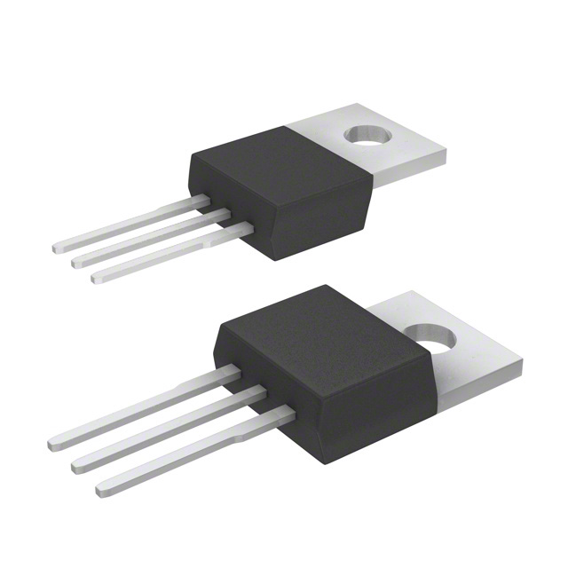
• 5-Lead Plastic DDPAK, 5-Lead TO-220 Package
Options (MCP1827)
• 3-Lead Plastic DDPAK, 3-Lead TO-220 Package
Options (MCP1827S)
The MCP1827/MCP1827S is a 1.5A Low Dropout
(LDO) linear regulator that provides high current and
low output voltages. The MCP1827 comes in a fixed or
adjustable output voltage version, with an output
voltage range of 0.8V to 5.0V. The 1.5A output current
capability, combined with the low output voltage
capability, make the MCP1827 a good choice for new
sub-1.8V output voltage LDO applications that have
high current demands. The MCP1827S is a 3-pin fixed
voltage version. The MCP1827/MCP1827S is based
upon the MCP1727 LDO device.
The MCP1827/MCP1827S is stable using ceramic
output capacitors that inherently provide lower output
noise and reduce the size and cost of the entire
regulator solution. Only 1 µF of output capacitance is
needed to stabilize the LDO.
Using CMOS construction, the quiescent current
consumed by the MCP1827/MCP1827S is typically
less than 120 µA over the entire input voltage range,
making it attractive for portable computing applications
that demand high output current. The MCP1827
versions have a Shutdown (SHDN) pin. When shut
down, the quiescent current is reduced to less than
0.1 µA.
On the MCP1827 fixed output versions the scaleddown output voltage is internally monitored and a
power good (PWRGD) output is provided when the
output is within 92% of regulation (typical). The
PWRGD delay is internally fixed at 200 µs (typical).
The overtemperature and short circuit current-limiting
provide additional protection for the LDO during system
Fault conditions.
Package Types
5-LD DDPAK
5-LD TO-220
Fixed/Adjustable
3-LD DDPAK
MCP1827S
MCP1827
MCP1827
1
2
VOUT
VIN
GND(TAB)
SHDN
VIN
GND(TAB)
VOUT
ADJ
SHDN
VIN
GND(TAB)
VOUT
PWRGD
2006-2013 Microchip Technology Inc.
MCP1827S
3
1 2 3 4 5
1 2 3 4 5
3-LD TO-220
1
2
3
VOUT
High-Speed Driver Chipset Power
Networking Backplane Cards
Notebook Computers
Network Interface Cards
Palmtop Computers
2.5V to 1.XV Regulators
VIN
•
•
•
•
•
•
GND(TAB)
Applications:
DS22001D-page 1
�MCP1827/MCP1827S
Typical Application
MCP1827 Fixed Output Voltage
PWRGD
R1
100 k
On
SHDN
Off
VIN = 2.3V to 2.8V
1 2 3 4 5
VOUT = 1.8V @ 1A
VOUT
VIN
GND
C1
4.7 µF
C2
1 µF
MCP1827 Adjustable Output Voltage
VADJ
R1
40 k
On
SHDN
Off
VIN = 2.3V to 2.8V
C1
4.7 µF
DS22001D-page 2
R2
20 k
1 2 3 4 5
VOUT
VIN
VOUT = 1.2V @ 1A
GND
C2
1 µF
2006-2013 Microchip Technology Inc.
�MCP1827/MCP1827S
Functional Block Diagram – Adjustable Output
PMOS
VIN
VOUT
Undervoltage
Lock Out
(UVLO)
ISNS
Cf
Rf
SHDN
ADJ
Overtemperature
Sensing
+
Driver w/limit
and SHDN
EA
–
SHDN
VREF
V IN
SHDN
Reference
Soft-Start
Comp
TDELAY
GND
92% of VREF
2006-2013 Microchip Technology Inc.
DS22001D-page 3
�MCP1827/MCP1827S
Functional Block Diagram – Fixed Output (5-pin)
PMOS
VIN
VOUT
Undervoltage
Lock Out
(UVLO)
Sense
ISNS
Cf
Rf
SHDN
Overtemperature
Sensing
+
Driver w/limit
and SHDN
EA
–
SHDN
VREF
V IN
SHDN
Reference
Soft-Start
Comp
TDELAY
PWRGD
GND
92% of VREF
DS22001D-page 4
2006-2013 Microchip Technology Inc.
�MCP1827/MCP1827S
Functional Block Diagram – Fixed Output (3-Pin)
PMOS
VIN
VOUT
Undervoltage
Lock Out
(UVLO)
Sense
ISNS
Cf
Rf
SHDN
Overtemperature
Sensing
+
Driver w/limit
and SHDN
EA
–
SHDN
VREF
VIN
SHDN
Reference
Soft-Start
Comp
TDELAY
GND
92% of VREF
2006-2013 Microchip Technology Inc.
DS22001D-page 5
�MCP1827/MCP1827S
1.0
ELECTRICAL
CHARACTERISTICS
Absolute Maximum Ratings †
VIN ....................................................................................6.5V
† Notice: Stresses above those listed under “Maximum Ratings” may cause permanent damage to the device. This is a
stress rating only and functional operation of the device at
those or any other conditions above those indicated in the
operational listings of this specification is not implied. Exposure to maximum rating conditions for extended periods may
affect device reliability.
Maximum Voltage on Any Pin .. (GND – 0.3V) to (VDD + 0.3)V
Maximum Power Dissipation ......... Internally-Limited (Note 6)
Output Short Circuit Duration ................................ Continuous
Storage temperature .....................................-65°C to +150°C
Maximum Junction Temperature, TJ ........................... +150°C
ESD protection on all pins (HBM/MM) 2 kV; 200V
AC/DC CHARACTERISTICS
Electrical Specifications: Unless otherwise noted, VIN = VOUT(MAX) + VDROPOUT(MAX) Note 1, VR=1.8V for Adjustable Output,
IOUT = 1 mA, CIN = COUT = 4.7 µF (X7R Ceramic), TA = +25°C. Boldface type applies for junction temperatures, TJ (Note 7) of
-40°C to +125°C
Parameters
Sym.
Min.
Input Operating Voltage
VIN
2.3
Input Quiescent Current
Iq
—
Input Quiescent Current for
SHDN Mode
ISHDN
Maximum Output Current
Max.
Units
6.0
V
120
220
µA
IL = 0 mA,
VOUT = 0.8V to 5.0V
—
0.1
3
µA
SHDN = GND
IOUT
1.5
—
—
A
VIN = 2.3V to 6.0V
VR = 0.8V to 5.0V
Line Regulation
VOUT/
(VOUT x VIN)
—
0.05
0.16
%/V
(Note 1) VIN 6V
Load Regulation
VOUT/VOUT
-1.0
±0.5
1.0
%
IOUT = 1 mA to 1.5A
(Note 4)
IOUT_SC
—
2.2
—
A
RLOAD < 0.1, Peak Current
VADJ
0.402
0.410
0.418
V
VIN = 2.3V to VIN = 6.0V,
IOUT = 1 mA
IADJ
-10
±0.01
+10
nA
VIN = 6.0V, VADJ = 0V to 6V
TCVOUT
—
40
—
ppm/°C
Note 3
VR - 2.5%
VR
±0.5%
VR + 2.5%
V
Note 2
Output Short Circuit Current
Typ.
Conditions
Adjust Pin Characteristics (Adjustable Output Only)
Adjust Pin Reference Voltage
Adjust Pin Leakage Current
Adjust Temperature Coefficient
Fixed-Output Characteristics (Fixed Output Only)
Voltage Regulation
Note 1:
2:
3:
4:
5:
6:
7:
VOUT
The minimum VIN must meet two conditions: VIN2.3V and VIN VOUT(MAX)VDROPOUT(MAX).
VR is the nominal regulator output voltage for the fixed cases. VR = 1.2V, 1.8V, etc. VR is the desired set point output
voltage for the adjustable cases. VR = VADJ * ((R1/R2)+1). Figure 4-1.
TCVOUT = (VOUT-HIGH – VOUT-LOW) *106 / (VR * Temperature). VOUT-HIGH is the highest voltage measured over the
temperature range. VOUT-LOW is the lowest voltage measured over the temperature range.
Load regulation is measured at a constant junction temperature using low duty-cycle pulse testing. Load regulation is
tested over a load range from 1 mA to the maximum specified output current.
Dropout voltage is defined as the input-to-output voltage differential at which the output voltage drops 2% below its
nominal value that was measured with an input voltage of VIN = VOUTMAX + VDROPOUT(MAX).
The maximum allowable power dissipation is a function of ambient temperature, the maximum allowable junction
temperature and the thermal resistance from junction to air. (i.e., TA, TJ, JA). Exceeding the maximum allowable power
dissipation will cause the device operating junction temperature to exceed the maximum +150°C rating. Sustained
junction temperatures above 150°C can impact device reliability.
The junction temperature is approximated by soaking the device under test at an ambient temperature equal to the
desired junction temperature. The test time is small enough such that the rise in the junction temperature over the
ambient temperature is not significant.
DS22001D-page 6
2006-2013 Microchip Technology Inc.
�MCP1827/MCP1827S
AC/DC CHARACTERISTICS (CONTINUED)
Electrical Specifications: Unless otherwise noted, VIN = VOUT(MAX) + VDROPOUT(MAX) Note 1, VR=1.8V for Adjustable Output,
IOUT = 1 mA, CIN = COUT = 4.7 µF (X7R Ceramic), TA = +25°C. Boldface type applies for junction temperatures, TJ (Note 7) of
-40°C to +125°C
Parameters
Sym.
Min.
Typ.
Max.
Units
VIN-VOUT
—
330
600
mV
VPWRGD_VIN
1.0
—
6.0
V
1.2
—
6.0
Conditions
Dropout Characteristics
Dropout Voltage
Note 5, IOUT = 1.5A,
VIN(MIN) = 2.3V
Power Good Characteristics
PWRGD Input Voltage Operating Range
TA = +25°C
TA = -40°C to +125°C
For VIN < 2.3V, ISINK = 100 µA
PWRGD Threshold Voltage
(Referenced to VOUT)
VPWRGD_TH
90
92
94
PWRGD Threshold Hysteresis
VPWRGD_HYS
1.0
2.0
3.0
%VOUT
PWRGD Output Voltage Low
VPWRGD_L
—
0.2
0.4
V
PWRGD Leakage
PWRGD_LK
—
1
—
nA
VPWRGD = VIN = 6.0V
TPG
—
200
—
µs
Rising Edge
RPULLUP = 10 k
TVDET-PWRGD
—
200
—
µs
VADJ or VOUT = VPWRGD_TH +
20 mV to VPWRGD_TH - 20 mV
Logic High Input
VSHDN-HIGH
45
%VIN
VIN = 2.3V to 6.0V
Logic Low Input
VSHDN-LOW
15
%VIN
VIN = 2.3V to 6.0V
+0.1
µA
VIN = 6V, SHDN =VIN,
SHDN = GND
µs
SHDN = GND to VIN
VOUT = GND to 95% VR
PWRGD Time Delay
Detect Threshold to PWRGD
Active Time Delay
%VOUT
89
92
95
Falling Edge
VOUT < 2.5V Fixed, VOUT = Adj.
VOUT >= 2.5V Fixed
IPWRGD SINK = 1.2 mA,
ADJ = 0V
Shutdown Input
SHDN Input Leakage Current
SHDNILK
-0.1
±0.001
AC Performance
Output Delay From SHDN
Output Noise
Power Supply Ripple Rejection
Ratio
Note 1:
2:
3:
4:
5:
6:
7:
TOR
100
eN
—
2.0
—
µV/Hz
PSRR
—
60
—
dB
IOUT = 200 mA, f = 1 kHz, COUT
= 10 µF (X7R Ceramic), VOUT =
2.5V
f = 100 Hz, COUT = 10 µF,
IOUT = 10 mA,
VINAC = 30 mV pk-pk,
CIN = 0 µF
The minimum VIN must meet two conditions: VIN2.3V and VIN VOUT(MAX)VDROPOUT(MAX).
VR is the nominal regulator output voltage for the fixed cases. VR = 1.2V, 1.8V, etc. VR is the desired set point output
voltage for the adjustable cases. VR = VADJ * ((R1/R2)+1). Figure 4-1.
TCVOUT = (VOUT-HIGH – VOUT-LOW) *106 / (VR * Temperature). VOUT-HIGH is the highest voltage measured over the
temperature range. VOUT-LOW is the lowest voltage measured over the temperature range.
Load regulation is measured at a constant junction temperature using low duty-cycle pulse testing. Load regulation is
tested over a load range from 1 mA to the maximum specified output current.
Dropout voltage is defined as the input-to-output voltage differential at which the output voltage drops 2% below its
nominal value that was measured with an input voltage of VIN = VOUTMAX + VDROPOUT(MAX).
The maximum allowable power dissipation is a function of ambient temperature, the maximum allowable junction
temperature and the thermal resistance from junction to air. (i.e., TA, TJ, JA). Exceeding the maximum allowable power
dissipation will cause the device operating junction temperature to exceed the maximum +150°C rating. Sustained
junction temperatures above 150°C can impact device reliability.
The junction temperature is approximated by soaking the device under test at an ambient temperature equal to the
desired junction temperature. The test time is small enough such that the rise in the junction temperature over the
ambient temperature is not significant.
2006-2013 Microchip Technology Inc.
DS22001D-page 7
�MCP1827/MCP1827S
AC/DC CHARACTERISTICS (CONTINUED)
Electrical Specifications: Unless otherwise noted, VIN = VOUT(MAX) + VDROPOUT(MAX) Note 1, VR=1.8V for Adjustable Output,
IOUT = 1 mA, CIN = COUT = 4.7 µF (X7R Ceramic), TA = +25°C. Boldface type applies for junction temperatures, TJ (Note 7) of
-40°C to +125°C
Parameters
Sym.
Min.
Typ.
Max.
Units
Thermal Shutdown Temperature
TSD
—
150
—
°C
IOUT = 100 µA, VOUT = 1.8V,
VIN = 2.8V
TSD
—
10
—
°C
IOUT = 100 µA, VOUT = 1.8V,
VIN = 2.8V
Thermal Shutdown Hysteresis
Note 1:
2:
3:
4:
5:
6:
7:
Conditions
The minimum VIN must meet two conditions: VIN2.3V and VIN VOUT(MAX)VDROPOUT(MAX).
VR is the nominal regulator output voltage for the fixed cases. VR = 1.2V, 1.8V, etc. VR is the desired set point output
voltage for the adjustable cases. VR = VADJ * ((R1/R2)+1). Figure 4-1.
TCVOUT = (VOUT-HIGH – VOUT-LOW) *106 / (VR * Temperature). VOUT-HIGH is the highest voltage measured over the
temperature range. VOUT-LOW is the lowest voltage measured over the temperature range.
Load regulation is measured at a constant junction temperature using low duty-cycle pulse testing. Load regulation is
tested over a load range from 1 mA to the maximum specified output current.
Dropout voltage is defined as the input-to-output voltage differential at which the output voltage drops 2% below its
nominal value that was measured with an input voltage of VIN = VOUTMAX + VDROPOUT(MAX).
The maximum allowable power dissipation is a function of ambient temperature, the maximum allowable junction
temperature and the thermal resistance from junction to air. (i.e., TA, TJ, JA). Exceeding the maximum allowable power
dissipation will cause the device operating junction temperature to exceed the maximum +150°C rating. Sustained
junction temperatures above 150°C can impact device reliability.
The junction temperature is approximated by soaking the device under test at an ambient temperature equal to the
desired junction temperature. The test time is small enough such that the rise in the junction temperature over the
ambient temperature is not significant.
TEMPERATURE SPECIFICATIONS
Electrical Specifications: Unless otherwise indicated, all limits apply for VIN = 2.3V to 6.0V.
Parameters
Sym.
Min.
Typ.
Max.
Units
Conditions
Operating Junction Temperature
Range
TJ
-40
—
+125
°C
Steady State
Maximum Junction Temperature
TJ
—
—
+150
°C
Transient
Storage Temperature Range
TA
-65
—
+150
°C
Thermal Resistance, 5LD DDPAK
JA
—
31.2
—
°C/W
4-Layer JC51 Standard Board
Thermal Resistance, 3LD DDPAK
JA
—
31.4
—
°C/W
4-Layer JC51 Standard Board
Thermal Resistance, 5LD TO-220
JA
—
29.3
—
°C/W
4-Layer JC51 Standard Board
Thermal Resistance, 3LD TO-220
JA
—
29.4
—
°C/W
4-Layer JC51 Standard Board
Temperature Ranges
Thermal Package Resistances
DS22001D-page 8
2006-2013 Microchip Technology Inc.
�MCP1827/MCP1827S
2.0
TYPICAL PERFORMANCE CURVES
Note:
The graphs and tables provided following this note are a statistical summary based on a limited number of
samples and are provided for informational purposes only. The performance characteristics listed herein
are not tested or guaranteed. In some graphs or tables, the data presented may be outside the specified
operating range (e.g., outside specified power supply range) and therefore outside the warranted range.
Note: Unless otherwise indicated, VOUT = 1.8V (Adjustable), VIN = 2.8V, COUT = 4.7 µF Ceramic (X7R), CIN = 4.7 µF
Ceramic (X7R), IOUT = 1 mA, Temperature = +25°C, VIN = VOUT + 0.6V, RPWRGD = 10 k To VIN.
Note: Junction Temperature (TJ) is approximated by soaking the device under test to an ambient temperature equal to
the desired Junction temperature. The test time is small enough such that the rise in Junction temperature over the
Ambient temperature is not significant.
Line Regulation (%/V)
Quiescent Current (μA)
150
140
130
130°C
90°C
120
25°C
110
-45°C
100
VOUT = 1.2V Adj
IOUT = 0 mA
90
2
3
4
5
0.1
0.09
0.08
0.07
0.06
0.05
0.04
0.03
0.02
0.01
0
VOUT = 1.2V adj
VIN = 2.3V to 6.0V
IOUT = 1 mA
IOUT = 1000 mA
IOUT = 100 mA
IOUT = 500 mA
-45
6
-20
5
30
105
130
FIGURE 2-4:
Line Regulation vs.
Temperature (1.2V Adjustable).
0.15
VIN=5.0V
V IN=3.3V
VOUT = 1.2V Adj
VIN=2.3V
Load Regulation (%)
Ground Current (µA)
FIGURE 2-1:
Quiescent Current vs. Input
Voltage (1.2V Adjustable).
200
190
180
170
160
150
140
130
120
110
100
80
Temperature (°C)
Input Voltage (V)
VOUT = 3.3V
0.10
IOUT = 1.0 mA to 1500 mA
0.05
0.00
VOUT = 0.8V
-0.05
VOUT = 1.8V
VOUT = 5.0V
-0.10
-0.15
0
250
500
750
1000
1250
-45
1500
-20
5
30
55
80
105
130
Temperature (°C)
Load Current (mA)
FIGURE 2-2:
Ground Current vs. Load
Current (1.2V Adjustable).
FIGURE 2-5:
Load Regulation vs.
Temperature (Adjustable Version).
0.411
140
IOUT = 0 mA
VOUT = 1.2V Adj
135
Adjust Pin Voltage (V)
Quiescent Current (μA)
55
130
125
120
VIN=5.0V
115
VIN=2.5V
110
VIN=4.0V
105
VIN = 6.0V
0.410
VIN = 5.0V
0.410
VIN = 2.3V
0.409
0.409
IOUT = 1.0 mA
0.408
100
-45
-20
5
30
55
80
105
130
-45
2006-2013 Microchip Technology Inc.
5
30
55
80
105
130
Temperature (°C)
Temperature (°C)
FIGURE 2-3:
Quiescent Current vs.
Junction Temperature (1.2V Adjustable).
-20
FIGURE 2-6:
Temperature.
Adjust Pin Voltage vs.
DS22001D-page 9
�MCP1827/MCP1827S
Note: Unless otherwise indicated, VOUT = 1.8V (Adjustable), VIN = 2.8V, COUT = 4.7 µF Ceramic (X7R), CIN = 4.7 µF
Ceramic (X7R), IOUT = 1 mA, Temperature = +25°C, VIN = VOUT + 0.6V, RPWRGD = 10 k To VIN.
150
VOUT = 5.0V Adj
0.30
Quiescent Current (μA)
Dropout Voltage (V)
0.35
0.25
0.20
VOUT = 2.5V Adj
0.15
0.10
0.05
VOUT = 0.8V
IOUT = 0 mA
140
+130°C
130
+85°C
120
+25°C
110
-45°C
100
90
80
0.00
0
250
500
750
1000
1250
2
1500
3
FIGURE 2-7:
Dropout Voltage vs. Load
Current (Adjustable Version).
0.36
VOUT = 3.3V Adj
VOUT = 2.5V Adj
0.32
Quiescent Current (μA)
Dropout Voltage (V)
150
VOUT = 5.0V Adj
0.34
VOUT = 2.5V
IOUT = 0 mA
140
+130°C
130
+90°C
120
+25°C
110
-45°C
100
90
80
0.30
-45
-20
5
30
55
80
105
3
130
3.5
4
FIGURE 2-8:
Dropout Voltage vs.
Temperature (Adjustable Version).
370
VIN = 4.5V
350
340
330
VIN = 5.0V
320
5.5
6
250.00
Ground Current (μA)
360
5
FIGURE 2-11:
Quiescent Current vs. Input
Voltage (2.5V Fixed).
VOUT = 3.3V Fixed
VIN = 3.9V
4.5
Input Voltage (V)
Temperature (°C)
Power Good Time Delay (µs)
6
FIGURE 2-10:
Quiescent Current vs. Input
Voltage (0.8V Fixed).
IOUT = 1.5A
0.40
0.38
5
Input Voltage (V)
Load Current (mA)
0.42
4
310
300
200.00
VOUT=0.8V
150.00
VOUT=2.5V
100.00
50.00
VIN = 2.3V for VR=0.8V
VIN = 3.1V for VR=2.5V
0.00
-45
-20
5
30
55
80
105
130
0
Temperature (°C)
FIGURE 2-9:
Power Good (PWRGD)
Time Delay vs. Temperature (Adjustable
Version).
DS22001D-page 10
250
500
750
1000
1250
1500
Load Current (mA)
FIGURE 2-12:
Current.
Ground Current vs. Load
2006-2013 Microchip Technology Inc.
�MCP1827/MCP1827S
Note: Unless otherwise indicated, VOUT = 1.8V (Adjustable), VIN = 2.8V, COUT = 4.7 µF Ceramic (X7R), CIN = 4.7 µF
Ceramic (X7R), IOUT = 1 mA, Temperature = +25°C, VIN = VOUT + 0.6V, RPWRGD = 10 k To VIN.
0.045
IOUT = 0 mA
125
Line Regulation (%/V)
Quiescent Current (μA)
130
120
115
110
VOUT = 0.8V
105
100
VOUT = 2.5V
95
-45
-20
5
VR = 2.5V
VIN = 3.1 to 6.0V
0.040
IOUT = 1 mA
0.035
0.030
IOUT = 100 mA
0.025
IOUT = 1000 mA
IOUT = 1500 mA
0.015
30
55
80
105
-45
130
-20
5
0.30
0.20
Load Regulation (%)
Ishdn (μA)
80
0.30
VR = 0.8V
VIN = 6.0V
0.15
VIN = 4.0V
0.10
VIN = 2.3V
0.05
105
130
VIN = 2.3V
VOUT = 0.8V
0.20
0.10
0.00
-0.10
IOUT = 1 mA to 1500 mA
-0.20
-0.30
0.00
-45
-20
5
30
55
80
105
-45
130
-20
5
ISHDN vs. Temperature.
FIGURE 2-14:
30
0.08
IOUT = 1 mA
IOUT = 1A
IOUT = 100 mA
IOUT = 500mA
VOUT = 0.8V
VIN = 2.3V to 6.0V
0.00
-45
-20
5
30
55
80
105
Temperature (°C)
FIGURE 2-15:
Line Regulation vs.
Temperature (0.8V Fixed).
2006-2013 Microchip Technology Inc.
130
Load Regulation (%)
0.00
-0.05
0.04
80
105
130
FIGURE 2-17:
Load Regulation vs.
Temperature (VOUT < 2.5V Fixed).
0.10
0.06
55
Temperature (°C)
Temperature (°C)
Line Regulation (%/V)
55
FIGURE 2-16:
Line Regulation vs.
Temperature (2.5V Fixed).
Quiescent Current vs.
0.25
0.02
30
Temperature (°C)
Temperature (°C)
FIGURE 2-13:
Temperature.
IOUT = 500 mA
0.020
IOUT = 1 mA to 1500 mA
-0.10
-0.15
VOUT = 2.5V
-0.20
-0.25
-0.30
VOUT = 5.0V
-0.35
-0.40
-0.45
-45
-20
5
30
55
80
105
130
Temperature (°C)
FIGURE 2-18:
Load Regulation vs.
Temperature (VOUT 2.5V Fixed).
DS22001D-page 11
�MCP1827/MCP1827S
Note: Unless otherwise indicated, VOUT = 1.8V (Adjustable), VIN = 2.8V, COUT = 4.7 µF Ceramic (X7R), CIN = 4.7 µF
Ceramic (X7R), IOUT = 1 mA, Temperature = +25°C, VIN = VOUT + 0.6V, RPWRGD = 10 k To VIN.
0.40
VR=0.8V, VIN=2.3V
VOUT = 2.5V
0.30
Noise (µV/ Hz)
Dropout Voltage (V)
10.000
Temperature = 25°C
0.35
0.25
VOUT = 5.0V
0.20
0.15
0.10
COUT=1 μF ceramic X7R
CIN=10 μF ceramic
1.000
IOUT=200 mA
VR=3.3V, VIN=4.1V
0.100
0.05
0.00
0
250
500
750
1000
1250
0.010
0.01
1500
0.1
Load Current (mA)
FIGURE 2-19:
Current.
Dropout Voltage vs. Load
1000
0
IOUT = 1.5A
-10
0.40
-20
0.35
VOUT = 5.0V
0.30
-45
-20
-30
-40
VR=1.2V Adj
COUT=10 μF ceramic X7R
VIN=3.1V
CIN=0 μF
IOUT=10 mA
-50
-60
VOUT = 2.5V
-70
0.25
5
30
55
80
105
-80
0.01
130
0.1
Temperature (°C)
FIGURE 2-20:
Temperature.
Dropout Voltage vs.
1
10
Frequency (kHz)
100
1000
FIGURE 2-23:
Power Supply Ripple
Rejection (PSRR) vs. Frequency (VOUT = 1.2V
Adj.).
0
3.00
-10
2.50
-20
PSRR (dB)
Short Circuit Current (A)
100
FIGURE 2-22:
Output Noise Voltage
Density vs. Frequency.
PSRR (dB)
Dropout Voltage (V)
0.45
1
10
Frequency (kHz)
2.00
1.50
1.00
VOUT = 2.5V
Temperature = 25°C
0.50
0.00
3.0
3.5
4.0
4.5
5.0
5.5
6.0
Input Voltage (V)
FIGURE 2-21:
Input Voltage.
DS22001D-page 12
Short Circuit Current vs.
-30
-40
VR=1.2V Adj
COUT=22 μF ceramic X7R
VIN=3.1V
CIN=0 μF
IOUT=10 mA
-50
-60
-70
-80
0.01
0.1
1
10
Frequency (kHz)
100
1000
FIGURE 2-24:
Power Supply Ripple
Rejection (PSRR) vs. Frequency (VOUT = 1.2V
Adj.).
2006-2013 Microchip Technology Inc.
�MCP1827/MCP1827S
Note: Unless otherwise indicated, VOUT = 1.8V (Adjustable), VIN = 2.8V, COUT = 4.7 µF Ceramic (X7R), CIN = 4.7 µF
Ceramic (X7R), IOUT = 1 mA, Temperature = +25°C, VIN = VOUT + 0.6V, RPWRGD = 10 k To VIN.
0
-10
PSRR (dB)
-20
-30
-40
VR=3.3V Fixed
COUT=10 μF ceramic X7R
VIN=3.9V
CIN=0 μF
IOUT=10 mA
-50
-60
-70
-80
0.01
0.1
1
10
Frequency (kHz)
100
1000
FIGURE 2-25:
Power Supply Ripple
Rejection (PSRR) vs. Frequency (VOUT = 3.3V
Fixed).
FIGURE 2-28:
Shutdown.
2.5V (Adj.) Startup from
FIGURE 2-29:
Timing.
Power Good (PWRGD)
FIGURE 2-30:
(3.3V Fixed).
Dynamic Line Response
0
-10
PSRR (dB)
-20
-30
-40
VR=3.3V Fixed
COUT=22 μF ceramic X7R
VIN=3.9V
CIN=0 μF
IOUT=10 mA
-50
-60
-70
-80
0.01
0.1
1
10
Frequency (kHz)
100
1000
FIGURE 2-26:
Power Supply Ripple
Rejection (PSRR) vs. Frequency (VOUT = 3.3V
Fixed).
FIGURE 2-27:
2.5V (Adj.) Startup from VIN.
2006-2013 Microchip Technology Inc.
DS22001D-page 13
�MCP1827/MCP1827S
Note: Unless otherwise indicated, VOUT = 1.8V (Adjustable), VIN = 2.8V, COUT = 4.7 µF Ceramic (X7R), CIN = 4.7 µF
Ceramic (X7R), IOUT = 1 mA, Temperature = +25°C, VIN = VOUT + 0.6V, RPWRGD = 10 k To VIN.
FIGURE 2-31:
Dynamic Load Response
(3.3V Fixed, 10 mA to 1500 mA).
DS22001D-page 14
FIGURE 2-32:
Dynamic Load Response
(3.3V Fixed, 100 mA to 1500 mA).
2006-2013 Microchip Technology Inc.
�MCP1827/MCP1827S
3.0
PIN DESCRIPTION
The descriptions of the pins are listed in Table 3-1.
TABLE 3-1:
PIN FUNCTION TABLE
3-Pin Fixed
Output
5-Pin Fixed
Output
Adjustable
Output
Name
Description
—
1
1
SHDN
Shutdown Control Input (active-low)
1
2
2
VIN
2
3
3
GND
Ground
Regulated Output Voltage
3.1
3
4
4
VOUT
—
5
—
PWRGD
—
—
5
ADJ
Voltage Adjust/Sense Input
Pad
Pad
Pad
EP
Exposed Pad of the Package (ground potential)
Input Voltage Supply (VIN)
Connect the unregulated or regulated input voltage
source to VIN. If the input voltage source is located
several inches away from the LDO, or the input source
is a battery, it is recommended that an input capacitor
be used. A typical input capacitance value of 1 µF to
10 µF should be sufficient for most applications.
3.2
Input Voltage Supply
Shutdown Control Input (SHDN)
Power Good Output
3.4
The PWRGD output is an open-drain output used to
indicate when the LDO output voltage is within 92%
(typically) of its nominal regulation value. The PWRGD
threshold has a typical hysteresis value of 2%. The
PWRGD output is delayed by 200 µs (typical) from the
time the LDO output is within 92% + 3% (max
hysteresis) of the regulated output value on power-up.
This delay time is internally fixed.
The SHDN input is used to turn the LDO output voltage
on and off. When the SHDN input is at a logic-high
level, the LDO output voltage is enabled. When the
SHDN input is pulled to a logic-low level, the LDO
output voltage is disabled. When the SHDN input is
pulled low, the PWRGD output also goes low and the
LDO enters a low quiescent current shutdown state
where the typical quiescent current is 0.1 µA.
3.5
3.3
3.6
Ground (GND)
Connect the GND pin of the LDO to a quiet circuit
ground. This will help the LDO power supply rejection
ratio and noise performance. The ground pin of the
LDO only conducts the quiescent current of the LDO
(typically 120 µA), so a heavy trace is not required.
For applications have switching or noisy inputs tie the
GND pin to the return of the output capacitor. Ground
planes help lower inductance and voltage spikes
caused by fast transient load currents and are
recommended for applications that are subjected to
fast load transients.
2006-2013 Microchip Technology Inc.
Power Good Output (PWRGD)
Output Voltage Adjust Input (ADJ)
For adjustable applications, the output voltage is
connected to the ADJ input through a resistor divider
that sets the output voltage regulation value. This
provides the user the capability to set the output
voltage to any value they desire within the 0.8V to 5.0V
range of the device.
Regulated Output Voltage (VOUT)
The VOUT pin is the regulated output voltage of the
LDO. A minimum output capacitance of 1.0 µF is
required for LDO stability. The MCP1827/MCP1827S is
stable with ceramic, tantalum and aluminum-electrolytic capacitors. See Section 4.3 “Output Capacitor”
for output capacitor selection guidance.
3.7
Exposed Pad (EP)
The DDPAK and TO-220 package have an exposed tab
on the package. A heat sink may be mount to the tab to
aid in the removal of heat from the package during
operation. The exposed tab is at the ground potential of
the LDO.
DS22001D-page 15
�MCP1827/MCP1827S
4.0
DEVICE OVERVIEW
EQUATION 4-2:
The MCP1827/MCP1827S is a high output current,
Low Dropout (LDO) voltage regulator. The low dropout
voltage of 330 mV typical at 1.5A of current makes it
ideal for battery-powered applications. Unlike other
high output current LDOs, the MCP1827/MCP1827S
only draws a maximum of 220 µA of quiescent current.
The MCP1827 has a shutdown control input and a
power good output.
4.1
The 5-pin MCP1827 LDO is available with either a fixed
output voltage or an adjustable output voltage. The
output voltage range is 0.8V to 5.0V for both versions.
The 3-pin MCP1827S LDO is available as a fixed
voltage device.
4.1.1
ADJUST INPUT
The adjustable version of the MCP1827 uses the ADJ
pin (pin 5) to get the output voltage feedback for output
voltage regulation. This allows the user to set the
output voltage of the device with two external resistors.
The nominal voltage for ADJ is 0.41V.
Figure 4-1 shows the adjustable version of the
MCP1827. Resistors R1 and R2 form the resistor
divider network necessary to set the output voltage.
With this configuration, the equation for setting VOUT is:
EQUATION 4-1:
VOUT
=
LDO Output Voltage
VADJ
=
ADJ Pin Voltage
(typically 0.41V)
MCP1827-ADJ
VOUT
On
SHDN
1
R1
2 3 4 5
ADJ
C2
1 µF
VIN
C1
4.7 µF
GND
=
LDO Output Voltage
VADJ
=
ADJ Pin Voltage
(typically 0.41V)
Output Current and Current
Limiting
The MCP1827/MCP1827S LDO is tested and ensured
to supply a minimum of 1.5A of output current. The
MCP1827/MCP1827S has no minimum output load, so
the output load current can go to 0 mA and the LDO will
continue to regulate the output voltage to within
tolerance.
The MCP1827/MCP1827S also incorporates an output
current limit. If the output voltage falls below 0.7V due
to an overload condition (usually represents a shorted
load condition), the output current is limited to 2.2A
(typical). If the overload condition is a soft overload, the
MCP1827/MCP1827S will supply higher load currents
of up to 3A. The MCP1827/MCP1827S should not be
operated in this condition continuously as it may result
in failure of the device. However, this does allow for
device usage in applications that have higher pulsed
load currents having an average output current value of
1.5A or less.
4.3
Off
VOUT
Output overload conditions may also result in an overtemperature shutdown of the device. If the junction
temperature rises above 150°C, the LDO will shut
down the output voltage. See Section 4.8
“Overtemperature Protection” for more information
on overtemperature shutdown.
R1 + R 2
V OUT = V ADJ ------------------
R2
Where:
Where:
4.2
LDO Output Voltage
VOUT – V ADJ
R1 = R2 --------------------------------
V ADJ
R2
FIGURE 4-1:
Typical adjustable output
voltage application circuit.
Output Capacitor
The MCP1827/MCP1827S requires a minimum output
capacitance of 1 µF for output voltage stability. Ceramic
capacitors are recommended because of their size,
cost and environmental robustness qualities.
Aluminum-electrolytic and tantalum capacitors can be
used on the LDO output as well. The Equivalent Series
Resistance (ESR) of the electrolytic output capacitor
must be no greater than 1 ohm. The output capacitor
should be located as close to the LDO output as is
practical. Ceramic materials X7R and X5R have low
temperature coefficients and are well within the
acceptable ESR range required. A typical 1 µF X7R
0805 capacitor has an ESR of 50 milli-ohms.
The allowable resistance value range for resistor R2 is
from 10 k to 200 k. Solving the equation for R1
yields the following equation:
DS22001D-page 16
2006-2013 Microchip Technology Inc.
�MCP1827/MCP1827S
Larger LDO output capacitors can be used with the
MCP1827/MCP1827S
to
improve
dynamic
performance and power supply ripple rejection. A
maximum of 22 µF is recommended. Aluminumelectrolytic capacitors are not recommended for lowtemperature applications of 25°C.
4.4
Input Capacitor
Low input source impedance is necessary for the LDO
output to operate properly. When operating from
batteries, or in applications with long lead length
(> 10 inches) between the input source and the LDO,
some input capacitance is recommended. A minimum
of 1.0 µF to 4.7 µF is recommended for most
applications.
For applications that have output step load
requirements, the input capacitance of the LDO is very
important. The input capacitance provides the LDO
with a good local low-impedance source to pull the
transient currents from in order to respond quickly to
the output load step. For good step response
performance, the input capacitor should be of
equivalent (or higher) value than the output capacitor.
The capacitor should be placed as close to the input of
the LDO as is practical. Larger input capacitors will also
help reduce any high-frequency noise on the input and
output of the LDO and reduce the effects of any
inductance that exists between the input source
voltage and the input capacitance of the LDO.
4.5
Power Good Output (PWRGD)
The PWRGD output is used to indicate when the output
voltage of the LDO is within 92% (typical value, see
Section 1.0 “Electrical Characteristics” for Minimum
and Maximum specifications) of its nominal regulation
value.
As the output voltage of the LDO rises, the PWRGD
output will be held low until the output voltage has
exceeded the power good threshold plus the hysteresis
value. Once this threshold has been exceeded, the
power good time delay is started (shown as TPG in the
Electrical Characteristics table). The power good time
delay is fixed at 200 µs (typical). After the time delay
period, the PWRGD output will go high, indicating that
the output voltage is stable and within regulation limits.
If the output voltage of the LDO falls below the power
good threshold, the power good output will transition
low. The power good circuitry has a 170 µs delay when
detecting a falling output voltage, which helps to
increase noise immunity of the power good output and
avoid false triggering of the power good output during
fast output transients. See Figure 4-2 for power good
timing characteristics.
2006-2013 Microchip Technology Inc.
When the LDO is put into Shutdown mode using the
SHDN input, the power good output is pulled low
immediately, indicating that the output voltage will be
out of regulation. The timing diagram for the power
good output when using the shutdown input is shown in
Figure 4-3.
The power good output is an open-drain output that can
be pulled up to any voltage that is equal to or less than
the LDO input voltage. This output is capable of sinking
1.2 mA (VPWRGD < 0.4V maximum).
VPWRGD_TH
VOUT
TPG
VOH
TVDET_PWRGD
PWRGD
VOL
FIGURE 4-2:
VIN
Power Good Timing.
TOR
30 µs
70 µs
TPG
SHDN
VOUT
PWRGD
FIGURE 4-3:
Shutdown.
4.6
Power Good Timing from
Shutdown Input (SHDN)
The SHDN input is an active-low input signal that turns
the LDO on and off. The SHDN threshold is a
percentage of the input voltage. The typical value of
this shutdown threshold is 30% of VIN, with minimum
and maximum limits over the entire operating
temperature range of 45% and 15%, respectively.
DS22001D-page 17
�MCP1827/MCP1827S
The SHDN input will ignore low-going pulses (pulses
meant to shut down the LDO) that are up to 400 ns in
pulse width. If the shutdown input is pulled low for more
than 400 ns, the LDO will enter Shutdown mode. This
small bit of filtering helps to reject any system noise
spikes on the shutdown input signal.
On the rising edge of the SHDN input, the shutdown
circuitry has a 30 µs delay before allowing the LDO
output to turn on. This delay helps to reject any false
turn-on signals or noise on the SHDN input signal. After
the 30 µs delay, the LDO output enters its soft-start
period as it rises from 0V to its final regulation value. If
the SHDN input signal is pulled low during the 30 µs
delay period, the timer will be reset and the delay time
will start over again on the next rising edge of the
SHDN input. The total time from the SHDN input going
high (turn-on) to the LDO output being in regulation is
typically 100 µs. See Figure 4-4 for a timing diagram of
the SHDN input.
TOR
400 ns (typ)
30 µs
70 µs
SHDN
Since the MCP1827/MCP1827S LDO undervoltage
lockout activates at 2.04V as the input voltage is falling,
the dropout voltage specification does not apply for
output voltages that are less than 1.9V.
For high-current applications, voltage drops across the
PCB traces must be taken into account. The trace
resistances can cause significant voltage drops
between the input voltage source and the LDO. For
applications with input voltages near 2.3V, these PCB
trace voltage drops can sometimes lower the input
voltage enough to trigger a shutdown due to
undervoltage lockout.
4.8
Overtemperature Protection
The MCP1827/MCP1827S LDO has temperaturesensing circuitry to prevent the junction temperature
from exceeding approximately 150°C. If the LDO
junction temperature does reach 150°C, the LDO
output will be turned off until the junction temperature
cools to approximately 140°C, at which point the LDO
output will automatically resume normal operation. If
the internal power dissipation continues to be
excessive, the device will again shut off. The junction
temperature of the die is a function of power
dissipation, ambient temperature and package thermal
resistance. See Section 5.0 “Application Circuits/
Issues” for more information on LDO power
dissipation and junction temperature.
VOUT
FIGURE 4-4:
Diagram.
4.7
Shutdown Input Timing
Dropout Voltage and Undervoltage
Lockout
Dropout voltage is defined as the input-to-output
voltage differential at which the output voltage drops
2% below the nominal value that was measured with a
VR + 0.6V differential applied. The MCP1827/
MCP1827S LDO has a very low dropout voltage
specification of 330 mV (typical) at 1.5A of output
current. See Section 1.0 “Electrical Characteristics”
for maximum dropout voltage specifications.
The MCP1827/MCP1827S LDO operates across an
input voltage range of 2.3V to 6.0V and incorporates
input Undervoltage Lockout (UVLO) circuitry that keeps
the LDO output voltage off until the input voltage
reaches a minimum of 2.18V (typical) on the rising
edge of the input voltage. As the input voltage falls, the
LDO output will remain on until the input voltage level
reaches 2.04V (typical).
DS22001D-page 18
2006-2013 Microchip Technology Inc.
�MCP1827/MCP1827S
5.0
APPLICATION CIRCUITS/
ISSUES
5.1
Typical Application
In addition to the LDO pass element power dissipation,
there is power dissipation within the MCP1827/
MCP1827S as a result of quiescent or ground current.
The power dissipation as a result of the ground current
can be calculated using the following equation:
The MCP1827/MCP1827S is used for applications that
require high LDO output current and a power good
output.
EQUATION 5-2:
P I GND = VIN MAX I VIN
Where:
VOUT = 2.5V @ 1.5A
MCP1827-2.5
On
Off
1 2 3 4 5
SHDN
R1
10 k
C2
10 µF
VIN
3.3V
C1
4.7 µF
GND
FIGURE 5-1:
5.1.1
Typical Application Circuit.
APPLICATION CONDITIONS
Package Type = TO-220-5
VIN maximum = 3.465V
VIN minimum = 3.135V
VDROPOUT (max) = 0.600V
VOUT (typical) = 2.5V
IOUT = 1.5A maximum
PDISS (typical) = 1.2W
Temperature Rise = 35.2°C
Power Calculations
5.2.1
=
Power dissipation due to the
quiescent current of the LDO
VIN(MAX)
=
Maximum input voltage
IVIN
=
Current flowing in the VIN pin
with no LDO output current
(LDO quiescent current)
PWRGD
Input Voltage Range = 3.3V ± 5%
5.2
PI(GND
POWER DISSIPATION
The internal power dissipation within the MCP1827/
MCP1827S is a function of input voltage, output
voltage, output current and quiescent current.
Equation 5-1 can be used to calculate the internal
power dissipation for the LDO.
EQUATION 5-1:
PLDO = V INMAX – V OUT MIN I OUT MAX
The total power dissipated within the MCP1827/
MCP1827S is the sum of the power dissipated in the
LDO pass device and the P(IGND) term. Because of the
CMOS construction, the typical IGND for the MCP1827/
MCP1827S is 120 µA. Operating at a maximum of
3.465V results in a power dissipation of 0.49 milliWatts. For most applications, this is small compared to
the LDO pass device power dissipation and can be
neglected.
The maximum continuous operating junction
temperature specified for the MCP1827/MCP1827S is
+125°C. To estimate the internal junction temperature
of the MCP1827/MCP1827S, the total internal power
dissipation is multiplied by the thermal resistance from
junction to ambient (RJA) of the device. The thermal
resistance from junction to ambient for the TO-220-5
package is estimated at 29.3° C/W.
EQUATION 5-3:
T J MAX = PTOTAL R JA + T A MAX
TJ(MAX) = Maximum continuous junction
temperature
PTOTAL = Total device power dissipation
RJA = Thermal resistance from junction to
ambient
TA(MAX) = Maximum ambient temperature
Where:
PLDO
=
LDO Pass device internal
power dissipation
VIN(MAX)
=
Maximum input voltage
VOUT(MIN)
=
LDO minimum output voltage
2006-2013 Microchip Technology Inc.
DS22001D-page 19
�MCP1827/MCP1827S
The maximum power dissipation capability for a
package can be calculated given the junction-toambient thermal resistance and the maximum ambient
temperature for the application. Equation 5-4 can be
used to determine the package maximum internal
power dissipation.
EQUATION 5-4:
P D MAX
T J MAX – T A MAX
= --------------------------------------------------R JA
PD(MAX) = Maximum device power dissipation
TJ(MAX) = maximum continuous junction
temperature
TA(MAX) = maximum ambient temperature
5.3
Typical Application
Internal power dissipation, junction temperature rise,
junction temperature and maximum power dissipation
is calculated in the following example. The power
dissipation as a result of ground current is small
enough to be neglected.
5.3.1
POWER DISSIPATION EXAMPLE
Package
Package Type = TO-220-5
Input Voltage
VIN = 3.3V ± 5%
LDO Output Voltage and Current
VOUT = 2.5V
RJA = Thermal resistance from junction to
ambient
IOUT = 1.5A
Maximum Ambient Temperature
EQUATION 5-5:
T J RISE = P D MAX R JA
TA(MAX) = 60°C
Internal Power Dissipation
PLDO(MAX) = (VIN(MAX) – VOUT(MIN)) x IOUT(MAX)
TJ(RISE) = Rise in device junction temperature
over the ambient temperature
PLDO = ((3.3V x 1.05) – (2.5V x 0.975))
x 1.5A
PD(MAX) = Maximum device power dissipation
PLDO = 1.54 Watts
RJA = Thermal resistance from junction to
ambient
EQUATION 5-6:
T J = T J RISE + T A
TJ = Junction temperature
TJ(RISE) = Rise in device junction temperature
over the ambient temperature
TA = Ambient temperature
5.3.1.1
Device Junction Temperature Rise
The internal junction temperature rise is a function of
internal power dissipation and the thermal resistance
from junction-to-ambient for the application. The
thermal resistance from junction-to-ambient (RJA) is
derived from EIA/JEDEC standards for measuring
thermal resistance. The EIA/JEDEC specification is
JESD51. The standard describes the test method and
board specifications for measuring the thermal
resistance from junction to ambient. The actual thermal
resistance for a particular application can vary
depending on many factors such as copper area and
thickness. Refer to AN792, “A Method to Determine
How Much Power a SOT23 Can Dissipate in an
Application” (DS00792), for more information regarding
this subject.
TJ(RISE) = PTOTAL x RJA
TJ(RISE) = 1.54 W x 29.3° C/W
TJ(RISE) = 45.12°C
DS22001D-page 20
2006-2013 Microchip Technology Inc.
�MCP1827/MCP1827S
5.3.1.2
Junction Temperature Estimate
To estimate the internal junction temperature, the
calculated temperature rise is added to the ambient or
offset temperature. For this example, the worst-case
junction temperature is estimated below:
TJ = TJ(RISE) + TA(MAX)
TJ = 45.12°C + 60.0°C
TJ = 105.12°C
As you can see from the result, this application will be
operating within the maximum operating junction
temperature of 125°C.
5.3.1.3
Maximum Package Power
Dissipation at 60°C Ambient
Temperature
TO-220-5 (29.3° C/W RJA):
PD(MAX) = (125°C – 60°C) / 29.3° C/W
PD(MAX) = 2.218W
DDPAK-5 (31.2°C/Watt RJA):
PD(MAX) = (125°C – 60°C)/ 31.2° C/W
PD(MAX) = 2.083W
From this table you can see the difference in maximum
allowable power dissipation between the TO-220-5
package and the DDPAK-5 package.
2006-2013 Microchip Technology Inc.
DS22001D-page 21
�MCP1827/MCP1827S
6.0
PACKAGING INFORMATION
6.1
Package Marking Information
3-Lead DDPAK (MCP1827S)
XXXXXXXXX
XXXXXXXXX
YYWWNNN
1
2
Example:
MCP1827S
e3
0.8EEB^^
0630256
3
1
2
3
3-Lead TO-220 (MCP1827S)
Example:
XXXXXXXXX
XXXXXXXXX
YYWWNNN
MCP1827S
12EAB^^
e3
0630256
1
2
1
3
5-Lead DDPAK (Fixed) (MCP1827)
2
3
Example:
XXXXXXXXX
XXXXXXXXX
YYWWNNN
MCP1827
e3
1.0EET^^
0630256
1 2 3 4 5
1 2 3 4 5
5-Lead TO-220 (Adj) (MCP1827)
Example:
XXXXXXXXX
XXXXXXXXX
YYWWNNN
MCP1827
e3
08EAT^^
0630256
1 2 3 4 5
1 2 3 4 5
Legend: XX...X
Y
YY
WW
NNN
e3
*
Note:
DS22001D-page 22
Customer-specific information
Year code (last digit of calendar year)
Year code (last 2 digits of calendar year)
Week code (week of January 1 is week ‘01’)
Alphanumeric traceability code
Pb-free JEDEC designator for Matte Tin (Sn)
This package is Pb-free. The Pb-free JEDEC designator ( e3 )
can be found on the outer packaging for this package.
In the event the full Microchip part number cannot be marked on one line, it will
be carried over to the next line, thus limiting the number of available
characters for customer-specific information.
2006-2013 Microchip Technology Inc.
�MCP1827/MCP1827S
��/HDG�3ODVWLF��(%��>''3$.@
1RWH�
)RU�WKH�PRVW�FXUUHQW�SDFNDJH�GUDZLQJV��SOHDVH�VHH�WKH�0LFURFKLS�3DFNDJLQJ�6SHFLILFDWLRQ�ORFDWHG�DW�
KWWS���ZZZ�PLFURFKLS�FRP�SDFNDJLQJ
E
E1
L1
D1
D
H
1
N
b
BOTTOM VIEW
e
TOP VIEW
b1
CHAMFER
OPTIONAL
C2
A
φ
c
A1
L
8QLWV
'LPHQVLRQ�/LPLWV
1XPEHU�RI�3LQV
,1&+(6
0,1
1
120
0$;
�
3LWFK
H
2YHUDOO�+HLJKW
$
����
�����%6&
±
6WDQGRII��
$�
����
±
����
2YHUDOO�:LGWK
(
����
±
����
([SRVHG�3DG�:LGWK
(�
����
±
±
0ROGHG�3DFNDJH�/HQJWK
'
����
±
����
2YHUDOO�/HQJWK
+
����
±
����
([SRVHG�3DG�/HQJWK
'�
����
±
±
/HDG�7KLFNQHVV
F
����
±
����
3DG�7KLFNQHVV
����
&�
����
±
����
/RZHU�/HDG�:LGWK
E
����
±
����
8SSHU�/HDG�:LGWK
E�
����
±
����
)RRW�/HQJWK
/
����
±
����
3DG�/HQJWK
/�
±
±
����
)RRW�$QJOH
�
�
±
�
1RWHV�
�� �6LJQLILFDQW�&KDUDFWHULVWLF�
�� 'LPHQVLRQV�'�DQG�(�GR�QRW�LQFOXGH�PROG�IODVK�RU�SURWUXVLRQV��0ROG�IODVK�RU�SURWUXVLRQV�VKDOO�QRW�H[FHHG�������SHU�VLGH�
�� 'LPHQVLRQLQJ�DQG�WROHUDQFLQJ�SHU�$60(�72����@
1RWH�
)RU�WKH�PRVW�FXUUHQW�SDFNDJH�GUDZLQJV��SOHDVH�VHH�WKH�0LFURFKLS�3DFNDJLQJ�6SHFLILFDWLRQ�ORFDWHG�DW�
KWWS���ZZZ�PLFURFKLS�FRP�SDFNDJLQJ
CHAMFER
OPTIONAL
φP
E
A
A1
Q
H1
D
D1
L1
L
b2
1
2
N
b
c
e
A2
e1
8QLWV
'LPHQVLRQ�/LPLWV
1XPEHU�RI�3LQV
,1&+(6
0,1
1
120
0$;
�
3LWFK
H
�����%6&
2YHUDOO�3LQ�3LWFK
H�
�����%6&
2YHUDOO�+HLJKW
$
����
±
����
7DE�7KLFNQHVV
$�
����
±
����
%DVH�WR�/HDG
$�
����
±
����
2YHUDOO�:LGWK
(
����
±
����
0RXQWLQJ�+ROH�&HQWHU
4
����
±
����
2YHUDOO�/HQJWK
'
����
±
����
0ROGHG�3DFNDJH�/HQJWK
'�
����
±
����
7DE�/HQJWK
+�
����
±
����
0RXQWLQJ�+ROH�'LDPHWHU
�3
����
±
����
/HDG�/HQJWK
/
����
±
����
/HDG�6KRXOGHU
/�
±
±
����
/HDG�7KLFNQHVV
F
����
±
����
/HDG�:LGWK
E
����
����
����
6KRXOGHU�:LGWK
E�
����
����
����
1RWHV�
�� 'LPHQVLRQV�'�DQG�(�GR�QRW�LQFOXGH�PROG�IODVK�RU�SURWUXVLRQV��0ROG�IODVK�RU�SURWUXVLRQV�VKDOO�QRW�H[FHHG�������SHU�VLGH�
�� 'LPHQVLRQLQJ�DQG�WROHUDQFLQJ�SHU�$60(�''3$.@
1RWH�
)RU�WKH�PRVW�FXUUHQW�SDFNDJH�GUDZLQJV��SOHDVH�VHH�WKH�0LFURFKLS�3DFNDJLQJ�6SHFLILFDWLRQ�ORFDWHG�DW�
KWWS���ZZZ�PLFURFKLS�FRP�SDFNDJLQJ
E1
E
L1
D1
D
H
1
N
b
BOTTOM VIEW
e
TOP VIEW
CHAMFER
OPTIONAL
C2
A
φ
c
A1
L
8QLWV
'LPHQVLRQ�/LPLWV
1XPEHU�RI�3LQV
,1&+(6
0,1
1
120
0$;
�
3LWFK
H
2YHUDOO�+HLJKW
$
����
±
6WDQGRII��
$�
����
±
����
2YHUDOO�:LGWK
(
����
±
����
([SRVHG�3DG�:LGWK
(�
����
±
±
0ROGHG�3DFNDJH�/HQJWK
'
����
±
����
2YHUDOO�/HQJWK
+
����
±
����
([SRVHG�3DG�/HQJWK
'�
����
±
±
/HDG�7KLFNQHVV
F
����
±
����
3DG�7KLFNQHVV
&�
����
±
����
E
����
±
����
)RRW�/HQJWK
/
����
±
����
3DG�/HQJWK
/�
±
±
����
/HDG�:LGWK
�����%6&
����
)RRW�$QJOH
�
�
±
�
1RWHV�
�� �6LJQLILFDQW�&KDUDFWHULVWLF�
�� 'LPHQVLRQV�'�DQG�(�GR�QRW�LQFOXGH�PROG�IODVK�RU�SURWUXVLRQV��0ROG�IODVK�RU�SURWUXVLRQV�VKDOO�QRW�H[FHHG�������SHU�VLGH�
�� 'LPHQVLRQLQJ�DQG�WROHUDQFLQJ�SHU�$60(�72����@
1RWH�
)RU�WKH�PRVW�FXUUHQW�SDFNDJH�GUDZLQJV��SOHDVH�VHH�WKH�0LFURFKLS�3DFNDJLQJ�6SHFLILFDWLRQ�ORFDWHG�DW�
KWWS���ZZZ�PLFURFKLS�FRP�SDFNDJLQJ
A
E
φP
CHAMFER
OPTIONAL
A1
Q
H1
D
D1
L
1
N
2 3
e
b
e1
c
A2
8QLWV
'LPHQVLRQ�/LPLWV
1XPEHU�RI�3LQV
,1&+(6
0,1
1
120
0$;
�
3LWFK
H
�����%6&
2YHUDOO�3LQ�3LWFK
H�
�����%6&
2YHUDOO�+HLJKW
$
����
±
2YHUDOO�:LGWK
(
����
±
����
2YHUDOO�/HQJWK
'
����
±
����
����
0ROGHG�3DFNDJH�/HQJWK
'�
����
±
����
7DE�/HQJWK
+�
����
±
����
7DE�7KLFNQHVV
$�
����
±
����
0RXQWLQJ�+ROH�&HQWHU
4
����
±
����
0RXQWLQJ�+ROH�'LDPHWHU
�3
����
±
����
/
����
±
����
$�
����
±
����
F
����
±
����
/HDG�/HQJWK
%DVH�WR�%RWWRP�RI�/HDG
/HDG�7KLFNQHVV
/HDG�:LGWK
E
����
����
����
1RWHV�
�� 'LPHQVLRQV�'�DQG�(�GR�QRW�LQFOXGH�PROG�IODVK�RU�SURWUXVLRQV��0ROG�IODVK�RU�SURWUXVLRQV�VKDOO�QRW�H[FHHG�������SHU�VLGH�
�� 'LPHQVLRQLQJ�DQG�WROHUDQFLQJ�SHU�$60(�