MCP19214/5
Digitally Enhanced Power Analog, Dual Channel, Low-Side PWM
Controller
Features
Microcontroller Features
• AEC Q100 Qualified and PPAP Capable
• Input Voltage Range: 4.5V-42V
• Two Independent High-Performance PWM
Controllers
• Two Independent Control Loops per Channel
allowing the User to Simultaneously Control the
Output Voltage and Current
• Can Be Configured to Control Multiple Topologies
including but Not Limited To:
- Boost
- Flyback
- Ćuk
- Single-Ended Primary-Inductor Converter
(SEPIC)
• Peak Current Mode Control
• Master/Slave Operation of the PWM Controllers
with Adjustable Phase Shift
• Differential Output Current Sense Capability
• Integrated Low-Side Current Sense Differential
Amplifier (10X)
• Integrated Low-Side Gate Drivers:
- 0.5A Sink/Source Current Capability at 5V
Supply Voltage
- 1A Sink/Source Current Capability at 10V
Supply Voltage
• Special Events Generator (the state of regulating
loops can be monitored without firmware
overhead)
• Configurable Parameters:
- Reference Voltages for Regulating Loops
(four internal DACs)
- Input Undervoltage Lockout (UVLO)
- Input Overvoltage Lockout (OVLO)
- Primary Current Leading Edge Blanking:
0 ns, 50 ns, 100 ns and 200 ns
- Fixed Switching Frequency Range:
31.25 kHz-2.0 MHz
- Slope Compensation
- Primary Current Sense Offset Adjustment
- Configurable GPIO Pin Options
• Low Quiescent Current: 10 mA Typical
• Low Sleep Current: 120 µA Typical
• Thermal Shutdown
• Precision 8 MHz Internal Oscillator Block:
- Factory-Calibrated to ±1%, Typical
• Interrupt-Capable
- Firmware
- Interrupt-on-Change Pins
• Only 35 Instructions to Learn
• 8192 Words On-Chip Program Memory
• 336 bytes of Internal RAM
• High-Endurance Flash:
- 100,000 Write Flash Endurance
- Flash Retention: > 40 Years
• Watchdog Timer (WDT) with Independent
Oscillator for Reliable Operation
• Programmable Code Protection
• In-Circuit Serial Programming™ (ICSP™) via Two
Pins
• Up to 12 I/O Pins and One Input-Only Pin
• Analog-to-Digital Converter (ADC):
- 10-Bit Resolution
- Internal 4096 mV Precision Reference
Generator
- Up to 8 External Channels
• Timer0: 8-Bit Timer/Counter with 8-Bit Prescaler
• Enhanced Timer1:
- 16-bit Timer with Prescaler
- Two Selectable Clock Sources
• Timer2: 8-Bit Timer with Prescaler
- 8-Bit Period Register
• I2C Communication:
- 7-bit Address Masking
- Two Dedicated Address Registers
• Addressable Universal Synchronous
Asynchronous Receiver Transmitter (AUSART)
(only MCP19215):
- 8 and 9-Bit Data Operations
- Address Detect
- Asynchronous and Synchronous Operating
Modes
2017 Microchip Technology Inc.
DS20005681A-page 1
�MCP19214/5
Pin Diagram – 28-Pin 5x5 QFN (MCP19214)
GPA0/AN0/TS_OUT1
GPA1/AN1
GPA2/AN2/T0CKI/INT
GPB4/AN5/CCD2/ICSPDAT
22 IP1
23 VFB1
24 VCOMP1
25 CCOMP1
ISP1
26
27 ISN1
GPB5/AN6/
28 ICSPCLK
MCP19214
5x5 QFN*
21 VIN
1
2
20 VDD
3
19 VDR
18 PDRV1
MCP19214
4
GPA3/AN3/TS_OUT2
5
17 PGND
GPA7/SCL
6
16 PDRV2
EXP-29
12
13
14
CCOMP2
VCOMP2
VFB2
10
ISN2
ISP2 11
9
GPA5/MCLR
15 IP2
GPA6/CCD1
7
8
GPB0/SDA
* Includes Exposed Thermal Pad (EP); see Table 1.
DS20005681A-page 2
2017 Microchip Technology Inc.
�MCP19214/5
Y
GPB4
4
GPA3
5
GPA7
GPB0
GPA5
GPA6
Basic
Y
3
Pull-Up
2
GPA2
Interrupt
GPA1
AUSART
Y
MSSP
1
Timers
ANSEL
GPA0
A/D
28-Pin QFN
28-PIN QFN (MCP19214) SUMMARY
I/O
TABLE 1:
AN0
—
—
—
IOC
Y
—
Analog Circuitry Debug Out(1)
AN1
—
—
—
IOC
Y
—
—
AN2
T0CKI
—
—
IOC
INT
Y
—
—
Y
AN5
—
—
—
IOC
Y
—
Dual Capture/Compare Input 2
Y
AN3
—
—
—
IOC
Y
6
N
—
—
SCL
—
IOC
Y
ICSPDAT —
7
N
—
—
SDA
—
IOC
Y
—
8
N
—
—
—
—
9
(2)
IOC
(3)
Y
Additional
Digital Circuitry Debug Out(1)
MCLR
Test Enable Input
N
—
—
—
—
IOC
Y
—
Dual Capture/Compare Input 1
ISN2
10 —
—
—
—
—
—
—
—
Current Sense Amplifier Negative
Input for PWM Channel 2
ISP2
11 —
—
—
—
—
—
—
—
Current Sense Amplifier Positive
Input for PWM Channel 2
CCOMP2 12 —
—
—
—
—
—
—
—
The Output of the Error Amplifier of
the Current Loop of PWM Channel 2
VCOMP2 13 —
—
—
—
—
—
—
—
The Output of the Error Amplifier of
the Voltage Loop of PWM Channel 2
VFB2
14 —
—
—
—
—
—
—
—
Feedback Input of the Voltage Loop
of PWM Channel 2
IP2
15 —
—
—
—
—
—
—
—
Primary Input Current Sense
of PWM Channel 2
PDRV2
16 —
—
—
—
—
—
—
—
Gate Drive Output of PWM Channel 2
PGND
17 —
—
—
—
—
—
—
—
Power Ground
PDRV1
18 —
—
—
—
—
—
—
—
Gate Drive Output of PWM Channel 1
VDR
19 —
—
—
—
—
—
—
—
Gate Drive Supply Voltage
VDD
20 —
—
—
—
—
—
—
—
VDD Output (+5V)
VIN
21 —
—
—
—
—
—
—
—
Input Supply Voltage
IP1
22 —
—
—
—
—
—
—
—
Primary Input Current Sense
of PWM Channel 1
VFB1
23 —
—
—
—
—
—
—
—
Feedback Input of the Voltage Loop
of PWM Channel 1
VCOMP1 24 —
—
—
—
—
—
—
—
The Output of the Error Amplifier of
the Voltage Loop of PWM Channel 1
CCOMP1 25 —
—
—
—
—
—
—
—
The Output of the Error Amplifier of
the Current Loop of PWM Channel 1
ISP1
26 —
—
—
—
—
—
—
—
Current Sense Amplifier Positive
Input for PWM Channel 1
ISN1
27 —
—
—
—
—
—
—
—
Current Sense Amplifier Negative
Input for PWM Channel 1
AN6
—
—
IOC
Y
—
—
—
—
GPB5
EP
Note 1:
2:
3:
28
Y
29 —
—
ICSPCLK —
AGND
Small Signal Ground and Digital
Ground
The Analog/Digital Debug Output is selected through the control of the ABECON1 register.
The IOC is disabled when MCLR is enabled.
Weak pull-up always enabled when MCLR is enabled, otherwise the pull-up is under user control.
2017 Microchip Technology Inc.
DS20005681A-page 3
�MCP19214/5
Pin Diagram – 32-PIN 5X5 QFN (MCP19215)
GPB6/AN7/TX/CK
ISN1
ISP1
CCOMP1
VCOMP1
VFB1
32
GPB1/AN4/RX/DT
GPB5/AN6/ICSPCLK
MCP19215
5x5 QFN*
31
30
29
28
27
26
25
GPA0/AN0/TS_OUT1
1
24 IP1
GPA1/AN1
2
23 VIN
22 VDD
GPA2/AN2/T0CKI/INT 3
21 VDR
GPB4/AN5/ICSPDAT 4
MCP19215
GPA3/AN3/TS_OUT2
5
20 PDRV1
GPA7/SCL
6
19 PGND
GPB0/SDA
18 PDRV2
7
EXP-33
17 IP2
9
10
11
12
13
14
15
16
GPA6/CCD1
AGND/DGND
ISN2
ISP2
CCOMP2
VCOMP2
VFB2
8
GPB7/CCD2
GPA5/MCLR
* Includes Exposed Thermal Pad (EP); see Table 2.
DS20005681A-page 4
2017 Microchip Technology Inc.
�MCP19214/5
32-Pin QFN
ANSEL
A/D
Timers
MSSP
AUSART
Interrupt
Pull-Up
32-PIN QFN (MCP19215) SUMMARY
I/O
TABLE 2:
Basic
GPA0
1
Y
AN0
—
—
—
IOC
Y
—
Analog Circuitry Debug Out(1)
GPA1
2
Y
AN1
—
—
—
IOC
Y
—
—
GPA2
3
Y
AN2 T0CKI
—
—
IOC
INT
Y
—
—
GPB4
4
Y
AN5
—
—
—
IOC
Y
GPA3
5
Y
AN3
—
—
—
IOC
Y
—
Digital Circuitry Debug Out(1)
GPA7
6
N
—
—
SCL
—
IOC
Y
—
Dual Capture/Single
Compare1 Input
GPB0
7
N
—
—
SDA
—
IOC
Y
—
—
MCLR
—
Additional
ICSPDAT —
GPA5
8
N
—
—
—
—
IOC(2)
Y(3)
GPB7
9
N
—
—
—
—
IOC
Y
—
—
GPA6
10
N
—
—
—
—
IOC
Y
—
—
AGND/DGND 11 —
—
—
—
—
—
—
—
—
ISN2
12 —
—
—
—
—
—
—
—
Current Sense Amplifier
Negative Input for PWM Channel
2
ISP2
13 —
—
—
—
—
—
—
—
Current Sense Amplifier
Positive Input for PWM Channel 2
CCOMP2
14 —
—
—
—
—
—
—
—
The Output of the Error Amplifier
of the Current Loop of PWM
Channel 2
VCOMP2
15 —
—
—
—
—
—
—
—
The Output of the Error Amplifier
of the Voltage Loop of PWM
Channel 2
VFB2
16 —
—
—
—
—
—
—
—
Feedback Input of the Voltage
Loop of PWM Channel 2
IP2
17 —
—
—
—
—
—
—
—
Primary Input Current Sense of
PWM Channel 2
PDRV2
18 —
—
—
—
—
—
—
—
Gate Drive Output of
PWM Channel 2
PGND
19 —
—
—
—
—
—
—
—
Power Ground
PDRV1
20 —
—
—
—
—
—
—
—
Gate Drive Output of
PWM Channel 1
VDR
21 —
—
—
—
—
—
—
—
Gate Drives Supply Voltage
VDD
22 —
—
—
—
—
—
—
—
VDD Output (+5V)
VIN
23 —
—
—
—
—
—
—
—
Input Supply Voltage
IP1
24 —
—
—
—
—
—
—
—
Primary Input Current Sense of
PWM Channel 1
VFB1
25 —
—
—
—
—
—
—
—
Feedback Input of the Voltage
Loop of PWM Channel 1
Note 1:
2:
3:
The Analog/Digital Debug Output is selected through the control of the ABECON1 register.
The IOC is disabled when MCLR is enabled.
Weak pull-up always enabled when MCLR is enabled, otherwise the pull-up is under user control.
2017 Microchip Technology Inc.
DS20005681A-page 5
�MCP19214/5
32-PIN QFN (MCP19215) SUMMARY (CONTINUED)
A/D
Timers
MSSP
AUSART
Interrupt
Pull-Up
Basic
VCOMP1
26 —
—
—
—
—
—
—
—
The Output of the Error Amplifier
of the Voltage Loop of PWM
Channel 1
CCOMP1
27 —
—
—
—
—
—
—
—
The Output of the Error Amplifier
of the Current Loop of PWM
Channel 1
ISP1
28 —
—
—
—
—
—
—
—
Current Sense Amplifier Positive
Input for PWM Channel 1
ISN1
29 —
—
—
—
—
—
—
—
Current Sense Amplifier Negative
Input for PWM Channel 1
I/O
ANSEL
32-Pin QFN
TABLE 2:
Additional
GPB6
30
Y
AN7
—
—
TX/CK
IOC
Y
—
—
GPB1
31
Y
AN4
—
—
RX/DT
IOC
Y
—
—
GPB5
32
Y
AN6
—
—
—
IOC
Y
—
—
—
—
—
—
EP
Note 1:
2:
3:
33 —
ICSPCLK —
—
—
The Analog/Digital Debug Output is selected through the control of the ABECON1 register.
The IOC is disabled when MCLR is enabled.
Weak pull-up always enabled when MCLR is enabled, otherwise the pull-up is under user control.
DS20005681A-page 6
2017 Microchip Technology Inc.
�MCP19214/5
Table of Contents
1.0 Device Overview .......................................................................................................................................................................... 9
2.0 Pin Description ........................................................................................................................................................................... 14
3.0 Functional Description................................................................................................................................................................ 19
4.0 Electrical Characteristics ............................................................................................................................................................ 22
5.0 Digital Electrical Characteristics ................................................................................................................................................. 29
6.0 Configuring the MCP19214/5 ..................................................................................................................................................... 37
7.0 Typical Performance Curves ...................................................................................................................................................... 51
8.0 System Bench Testing................................................................................................................................................................ 55
9.0 Device Calibration ...................................................................................................................................................................... 59
10.0 Memory Organization ................................................................................................................................................................. 75
11.0 Device Configuration .................................................................................................................................................................. 89
12.0 Resets ........................................................................................................................................................................................ 91
13.0 Interrupts .................................................................................................................................................................................... 99
14.0 Watchdog Timer (WDT)............................................................................................................................................................. 111
15.0 Interrupt-On-Change .................................................................................................................................................................113
16.0 Oscillator Modes........................................................................................................................................................................117
17.0 Flash Program Memory Control ................................................................................................................................................119
18.0 I/O Ports ................................................................................................................................................................................... 125
19.0 Power-Down Mode (Sleep) ...................................................................................................................................................... 133
20.0 Analog-to-Digital Converter (ADC) Module .............................................................................................................................. 135
21.0 Timer0 Module ......................................................................................................................................................................... 145
22.0 Timer1 Module ......................................................................................................................................................................... 147
23.0 Timer2 Module ......................................................................................................................................................................... 151
24.0 Enhanced PWM Module........................................................................................................................................................... 153
25.0 Internal Temperature Indicator Module..................................................................................................................................... 157
26.0 PWM Control Logic .................................................................................................................................................................. 159
27.0 Master Synchronous Serial Port (MSSP) Module .................................................................................................................... 161
28.0 Addressable Universal Synchronous Asynchronous Receiver Transmitter (AUSART) ........................................................... 205
29.0 Application Hints....................................................................................................................................................................... 215
30.0 Instruction Set Summary .......................................................................................................................................................... 219
31.0 Dual Capture/Compare (CCD) Module .................................................................................................................................... 229
32.0 In-Circuit Serial Programming™ (ICSP™) ............................................................................................................................... 233
33.0 Development Support............................................................................................................................................................... 235
34.0 Packaging Information.............................................................................................................................................................. 239
Appendix A: Revision History............................................................................................................................................................. 247
Index .................................................................................................................................................................................................. 249
The Microchip Web Site ..................................................................................................................................................................... 255
Customer Change Notification Service .............................................................................................................................................. 255
Customer Support .............................................................................................................................................................................. 255
Product Identification System ............................................................................................................................................................ 257
Trademarks ........................................................................................................................................................................................ 259
Worldwide Sales and Service ............................................................................................................................................................ 260
2017 Microchip Technology Inc.
DS20005681A-page 7
�MCP19214/5
TO OUR VALUED CUSTOMERS
It is our intention to provide our valued customers with the best documentation possible to ensure successful use of your Microchip
products. To this end, we will continue to improve our publications to better suit your needs. Our publications will be refined and
enhanced as new volumes and updates are introduced.
If you have any questions or comments regarding this publication, please contact the Marketing Communications Department via
e-mail at docerrors@microchip.com. We welcome your feedback.
Most Current Data Sheet
To obtain the most up-to-date version of this data sheet, please register at our web site at:
www.microchip.com
You can determine the version of a data sheet by examining its literature number found on the bottom outside corner of any page.
The last character of the literature number is the version number (e.g., DS30000000A is version A of document DS30000000).
Errata
An errata sheet, describing minor operational differences from the data sheet and recommended workarounds, may exist for current
devices. As device/documentation issues become known to us, we will publish an errata sheet. The errata will specify the revision
of silicon and revision of document to which it applies.
To determine if an errata sheet exists for a particular device, please check with one of the following:
• Microchip’s web site; www.microchip.com
• Your local Microchip sales office (see last page)
When contacting a sales office, please specify which device, revision of silicon and data sheet (include literature number) you are
using.
Customer Notification System
Register on our web site at www.microchip.com to receive the most current information on all of our products.
DS20005681A-page 8
2017 Microchip Technology Inc.
�MCP19214/5
1.0
DEVICE OVERVIEW
The MCP19214/5 devices are highly integrated,
digitally enhanced PWM controllers, used for battery
chargers, bidirectional converters, LED lighting
systems and other low-side switch PWM applications.
These devices feature two independent analog PWM
controllers, and the internal architecture is optimized
for applications that require precise control of the
output parameters. Like the other members of the
digitally
enhanced
PWM
controllers
family,
MCP19214/5 includes a fully programmable
microcontroller core and a 10-bit analog-to-digital
converter.
Each PWM channel includes two error amplifiers with
independent adjustable reference voltage generators,
current sense input with programmable leading edge
blanking, programmable slope compensation ramp
generator, integrated internal programmable oscillator,
current sense differential amplifier and an integrated
MOSFET driver.
An internal LDO (+5V) is used to power the PIC core,
the analog circuitry and to provide 5V externally. This
5V external output can also be used to supply the
internal MOSFET drivers. The internal MOSFET
drivers have the option to be powered from an external
voltage source (up to 10V) in order to accommodate
applications that require higher voltages for gate
driving.
The MCP19214 is packaged in a 28-lead
5 mm x 5 mm QFN, and the MCP19215 in a 32-lead
5 mm x 5 mm QFN. The operating input voltage for
normal device operation is 4.5V-42V, with an absolute
maximum of 44V. The maximum transient voltage is
48V for 500 mS.
Power trains supported by this architecture include, but
are not limited to, Boost, Buck-Boost, Flyback, SEPIC
and Cuk.
MCP19214/5 integrates an I2C controller and an
Addressable Universal Synchronous Asynchronous
Receiver Transmitter (AUSART) module (only for
MCP19215). The user can develop specific
communication protocols using the internal interfaces.
A PMBus compatible protocol, specific for power
converters, can be implemented using the provided
I2C serial bus.
Complete customization of the device operating
parameters, start-up or shutdown profiles, protection
levels and fault handling procedures are accomplished
by firmware that can be developed using Microchip’s
MPLAB® X Integrated Development Environment.
Programming the MCP19214/5 is done using one of
Microchip’s many in-circuit debugger and device
programmers.
The MCP19214/5 controllers offer a very high degree
of integration, allowing the user to develop complex
applications without additional circuitry. Some unique
features, like simultaneous control of the converter’s
output current and voltage, make MCP19214/5
devices ideally suited for battery chargers, LED drivers
and bidirectional converters. Additionally, the General
Purpose Inputs/Outputs (GPIOs) can be used to drive
various switches, to enable/disable additional circuitry,
or to indicate a typical state.
2017 Microchip Technology Inc.
DS20005681A-page 9
�MCP19214/5
FIGURE 1-1:
MCP19214/5 SIMPLIFIED INTERNAL BLOCK DIAGRAM
2048
mV
BGAP
6 bit
V''
LDO
VIN
UVLO
VREF1
UVLO
V''
OVLO
V''
OVLO
8 bit
Ȉ
IREF1
Vref1
VREF2
Iref 1
Vpedestal
Vref2
8 bit
Ȉ
IREF2
R
Iref 2
Vpedestal
V''
OK
V''OK_ref -
1024
mV
8 bit
4096
mV
6 bit
+
8 bit
R
V''
V''
Vsns1
EA 2
+
VFB1
Vref1
100
μA
200
μA
3V
VCOMP1
V''
Iref1
+
EA 1
-
Slope
Comp 1
+ Ȉ
200
μA
6 bit
AV'' PWM1
S
+
PWM
-
R
SET
CLR
Q
Q
+ Ȉ
VDR
+
4 bit
OFF
CCOMP1
PDRV1
3V
DRV1
2 bit
LEB
IP1
VDR
0V
PGOOD
IV_GOOD
Control
Logic
VDR
VDR
UVLO
IV_DOM
Vpedestal
Vpedestal
V''
VDR
V''
ISP1
+
A1
-
ISN1
ISN1
+
-A
2
PDRV2
Isns
DRV2
Vpedestal A=2
PWM Channel #1
Common for both channels
A=10
VFB2
VCOMP2
CCOMP2
IP2
ISP2
ISN2
PWM Channel #2
OVLO UVLO
V''
OK
PGOOD1 PGOOD2
Interrupt Generator
Isns1 Vsns1 Isns2 Vsns2
PWM 1 PWM 2
Clock
Generator
INT
PWM
EN2
EN1
AN1
AN2
PIC Micro Core
MUX
MCLR
DS20005681A-page 10
SDA
SCL
IOs
2017 Microchip Technology Inc.
�MCP19214/5
FIGURE 1-2:
MCP19214 DUAL LED STRING APPLICATION DIAGRAM
VIN
VIN
VDD
VDR
PDRV1
IP1
ISP1
PWM Ch. 1
ISN1
VFB1
VCOMP1
ICOMP1
8
I/O
PDRV2
IP2
PWM Ch. 2
ISP2
MCP19214
ISN2
VFB2
VCOMP2
ICOMP2
Second Flyback
Channel
AGND
2017 Microchip Technology Inc.
PGND
DS20005681A-page 11
�MCP19214/5
FIGURE 1-3:
MCP19214 BIDIRECTIONAL CONVERTER APPLICATION DIAGRAM
Current-limited Voltage Regulated Source
Voltage-limited Current Source
COUT
CIN
Q1
VIN
V''
Battery
T1
Input/
Output
Voltage
Q2
VDR
PDRV1
GPA5/MCLR
GPB5/AN6/ICSPCLK
IP1
GPB4/AN5//ICSPDAT
ISP1
ISN1
VFB1
GPA0/AN0
GPA2/AN2/T0CKI/INT
VCOMP1
GPA6/CCD1
CCOMP1
MCP19214
VFB2
IP2
PDRV2
Comm
ISP2
GPB0/SDA
GPA7/SCL
ISN2
VCOMP2
CCOMP2
PAD
DS20005681A-page 12
PGND
2017 Microchip Technology Inc.
�MCP19214/5
FIGURE 1-4:
MICROCONTROLLER CORE BLOCK DIAGRAM
Configuration
13
Flash
8K x 14
Program
Memory
8
Data Bus
Program Counter
PORTA
GPA0
GPA1
GPA2
GPA3
RAM
336
bytes
File
Registers
8 Level Stack
(13-bit)
Program
14
Bus
RAM Addr
GPA5
GPA6
GPA7
9
Addr MUX
Instruction reg
Direct Addr
7
8
PORTB
Indirect
Addr
GPB0
GPB1 (Note 1)
FSR reg
STATUS reg
8
3
Instruction
Decode &
Control
TESTCLKIN
Timing
Generation
GPB4
GPB5
GPB6 (Note 1)
GPB7 (Note 1)
MUX
Power-up
Timer
ALU
Power-on
Reset
8
8 MHz Internal
Oscillator
MCLR VIN VSS
USART
TX
RX
PMDATL
Self read/
write flash
memory
Timer1
Timer2
T0CKI
Analog interface
registers
SDA
SCL
W reg
Watchdog
Timer
Timer0
I2C
Enhanced
PWM
CCD
CCD1
EEADDR
CCD2
Note 1: MCP19215 only
2017 Microchip Technology Inc.
DS20005681A-page 13
�MCP19214/5
2.0
PIN DESCRIPTION
The 28-lead MCP19214 and 32-lead MCP19215
devices feature pins that have multiple functions
associated with each pin. Table 2-1 provides a
description of the different functions. Refer to
Section 2.1 “Detailed Pin Functional Description”
for more detailed information.
TABLE 2-1:
MCP19214/5 PINOUT DESCRIPTION
Name
GPA0/AN0/TS_OUT1
GPA1/AN1
GPA2/AN2/T0CKI/INT
GPA3/AN3/TS_OUT2
Function
Input
Type
Output
Type
GPA0
TTL
AN0
AN
—
A/D Channel 0 input
TS_OUT1
—
—
Internal analog signal multiplexer output(1)
GPA1
TTL
AN1
AN
CMOS General-purpose I/O
CMOS General-purpose I/O
—
GPA6/CCD1
GPA7/SCL
GPB0/SDA
GPB1/AN4/RX/DT
(MCP19215 Only)
GPB4/AN5/ICSPDAT
GPB5/AN6/ICSPCLK
A/D Channel 1 input
GPA2
ST
AN2
AN
—
A/D Channel 2 input
T0CKI
ST
—
Timer0 clock input
—
External interrupt
INT
ST
GPA3
TTL
AN3
AN
CMOS General-purpose I/O
CMOS General-purpose I/O
—
A/D Channel 3 input
Internal digital signals multiplexer output(1)
TS_OUT2
GPA5/MCLR
Description
GPA5
TTL
—
General-purpose input only
MCLR
ST
—
Master Clear with internal pull-up
GPA6
ST
CMOS General-purpose I/O
CCD1
ST
CMOS Single Compare output of PWM channel 1.
Dual Capture input of PWM channel 1.
GPA7
ST
CMOS General-purpose open drain I/O
SCL
I2C
GPB0
TTL
SDA
I2C
GPB1
TTL
AN4
AN
—
A/D Channel 4 input
RX
ST
—
AUSART asynchronous receive input
DT
TTL
CMOS AUSART synchronous data input/output
GPB4
TTL
CMOS General-purpose I/O
AN5
AN
OD
I2C clock
CMOS General-purpose I/O
OD
I2C data input/output
CMOS General-purpose I/O
—
A/D Channel 5 input
ICSPDAT
ST
CMOS In-Circuit Debugger and ICSP programming data
GPB5
TTL
CMOS General-purpose I/O
AN6
AN
—
A/D Channel 6 input
ISCPCLK
ST
—
In-Circuit Debugger and ICSP programming clock
Legend:
AN = Analog input or output
TTL = TTL compatible input
Note 1:
The Analog/Digital Debug Output is selected through the control of the ABECON1 register.
DS20005681A-page 14
CMOS = CMOS compatible input or output
ST = Schmitt Trigger input with CMOS levels
OD = Open-Drain
I2C = Schmitt Trigger input with I2C
2017 Microchip Technology Inc.
�MCP19214/5
TABLE 2-1:
MCP19214/5 PINOUT DESCRIPTION (CONTINUED)
Name
GPB6/AN7/TX/CK
(MCP19215 Only)
GPB7/CCD2
(MCP19215 Only)
Function
Input
Type
GPB6
TTL
AN7
AN
Output
Type
Description
CMOS General-purpose I/O
—
A/D Channel 7 input
TX
—
CK
TTL
CMOS AUSART synchronous clock input/output
CMOS AUSART asynchronous transmit output
GPB7
TTL
CMOS General-purpose I/O
CCD2
ST
CMOS Single Compare output of PWM channel 2
Dual Capture input of PWM channel 2
VIN
VIN
—
—
Device input supply voltage
VDD
VDD
—
—
Internal +5V LDO output pin
VDR
—
—
Gate drivers supply voltage
AGND
—
—
Small signal quiet ground
VDR
AGND/DGND
PGND
PGND
—
—
Large signal power ground
PDRV1
PDRV1
—
—
Primary PWM channel MOSFET gate drive
PDRV2
PDRV2
—
—
Secondary PWM channel MOSFET gate drive
IP1
—
—
Primary input current sense for PWM channel 1
IP1
IP2
IP2
—
—
Primary input current sense for PWM channel 2
ISN1
ISN1
—
—
Differential current sense amplifier negative input
of PWM channel 1
ISN2
ISN2
—
—
Differential current sense amplifier negative input
of PWM channel 2
ISP1
ISP1
—
—
Differential current sense amplifier positive input of
PWM channel 1
ISP2
ISP2
—
—
Differential current sense amplifier positive input of
PWM channel 2
CCOMP1
CCOMP1
—
—
Output of the current loop error amplifier of PWM
channel 1
CCOMP2
CCOMP2
—
—
Output of the current loop error amplifier of PWM
channel 2
VCOMP1
VCOMP1
—
—
Output of the voltage loop error amplifier of PWM
channel 1
VCOMP2
VCOMP2
—
—
Output of the voltage loop error amplifier of PWM
channel 2
VFB1
VFB1
—
—
Feedback input of the voltage loop of PWM
channel 1
VFB2
VFB2
—
—
Feedback input of the voltage loop of PWM
channel 2
EP
Exposed Pad. The AGND and DGND internal nodes
close here. Connect this to the PCBs ground plane
using multiple vias.
Legend:
AN = Analog input or output
TTL = TTL compatible input
Note 1:
The Analog/Digital Debug Output is selected through the control of the ABECON1 register.
2017 Microchip Technology Inc.
CMOS = CMOS compatible input or output
ST = Schmitt Trigger input with CMOS levels
OD = Open-Drain
I2C = Schmitt Trigger input with I2C
DS20005681A-page 15
�MCP19214/5
2.1
2.1.1
Detailed Pin Functional
Description
GPA0 PIN
2.1.5
GPA5 PIN
GPA5 is a general-purpose TTL input only pin. An
internal weak pull-up and interrupt-on-change are also
available.
GPA0 is a general-purpose TTL input or CMOS output
pin whose data direction is controlled in TRISGPA. An
internal weak pull-up and interrupt-on-change are also
available.
For programming purposes, this pin is to be connected
to the MCLR pin of the serial programmer. Refer to
Section 32.0 “In-Circuit Serial Programming™
(ICSP™)” for more information.
AN0 is an input to the A/D. To configure this pin to be
read by the A/D on channel 0, bits TRISA0 and ANSA0
must be set.
This pin is MCLR when the MCLRE bit is set in the
CONFIG register. When the MCLR is active, the
interrupt-on-change is disabled and the weak pull-up
is always enabled.
The ABECON1/2 registers can be configured to set this
pin to the TS_OUT1 function. It is a buffered output of
the internal analog signals multiplexer. Analog signals
present on this pin are controlled by the ADCON0
register.
2.1.2
GPA1 PIN
GPA1 is a general-purpose TTL input or CMOS output
pin whose data direction is controlled in TRISGPA. An
internal weak pull-up and interrupt-on-change are also
available.
AN1 is an input to the A/D. To configure this pin to be
read by the A/D on channel 1, bits TRISA1 and ANSA1
must be set.
2.1.3
GPA2 PIN
GPA2 is a general-purpose ST input or CMOS output
pin whose data direction is controlled in TRISGPA. An
internal weak pull-up and interrupt-on-change are also
available.
2.1.6
GPA6 PIN
GPA6 is a general-purpose CMOS output ST input pin
whose data direction is controlled in TRISGPA.
GPA6 is part of the CCD Module. For more information,
refer to Section 31.0 “Dual Capture/Compare (CCD)
Module”.
2.1.7
GPA7 PIN
GPA7 is a general-purpose TTL input or CMOS output
pin whose data direction is controlled in TRISGPA. An
internal weak pull-up and interrupt-on-change are also
available.
When the MCP19214/5 is configured for I2C
communication, Section 27.2 “I2C Mode Overview”,
GPA7 functions as the I2C clock (SCL). This pin must
be configured as an input to allow proper operation.
AN2 is an input to the A/D. To configure this pin to be
read by the A/D on channel 2, bits TRISA2 and ANSA2
must be set.
When bit T0CS is set in the OPTION_REG register, the
T0CKI function is enabled. Refer to Section 21.0
“Timer0 Module” for more information.
GPA2 can also be configured as an external interrupt
by setting the INTE bit. Refer to Section 13.2
“GPA2/INT Interrupt” for more information.
2.1.4
GPA3 PIN
GPA3 is a general-purpose TTL input or CMOS output
pin whose data direction is controlled in TRISGPA. An
internal weak pull-up and interrupt-on-change are also
available.
AN3 is an input to the A/D. To configure this pin to be
read by the A/D on channel 3, bits TRISA3 and ANSA3
must be set.
The ABECON1/2 registers can be configured to set this
pin to the TS_OUT2 function. It is a buffered output of
the internal digital signals multiplexer. Digital signals
present on this pin are controlled by the ABECON2
register.
DS20005681A-page 16
2017 Microchip Technology Inc.
�MCP19214/5
2.1.8
GPB0 PIN
2.1.12
GPB6 PIN (MCP19215 ONLY)
GPB0 is a general-purpose TTL input or CMOS output
pin whose data direction is controlled in TRISGPB. An
internal weak pull-up and interrupt-on-change are also
available.
GPB6 is a general-purpose TTL input or CMOS output
pin whose data direction is controlled in TRISGPB. An
internal weak pull-up and interrupt-on-change are also
available.
When the MCP19214/5 are configured for I2C
communication, Section 27.2 “I2C Mode Overview”,
GPB0 functions as the I2C clock (SDA). This pin must
be configured as an input to allow proper operation.
AN7 is an input to the A/D. To configure this pin to be
read by the A/D on channel 7, bits TRISB6 and ANSB6
must be set.
2.1.9
GPB1 PIN (MCP19215 ONLY)
GPB1 is a general-purpose TTL input or CMOS output
pin whose data direction is controlled in TRISGPB. An
internal weak pull-up and interrupt-on-change are also
available.
AN4 is an input to the A/D. To configure this pin to be
read by the A/D on channel 4, bits TRISB1 and ANSB1
must be set.
RX is the receiver’s input of the AUSART block for
asynchronous operation.
DT is the input/output pin of the AUSART block for
synchronous operation
2.1.10
GPB4 PIN
GPB4 is a general-purpose TTL input or CMOS output
pin whose data direction is controlled in TRISGPB. An
internal weak pull-up and interrupt-on-change are also
available.
AN5 is an input to the A/D. To configure this pin to be
read by the A/D on channel 5, bits TRISB4 and ANSB4
must be set.
ICSPDAT is the serial programming data I/O function.
This is used in conjunction with ICSPCLK to serial
program the device. Refer to Section 32.0 “In-Circuit
Serial Programming™ (ICSP™)” for more
information.
2.1.11
GPB5 PIN
GPB5 is a general-purpose TTL input or CMOS output
pin whose data direction is controlled in TRISGPB. An
internal weak pull-up and interrupt-on-change are also
available.
AN6 is an input to the A/D. To configure this pin to be
read by the A/D on channel 6, bits TRISB5 and ANSB5
must be set.
ICSPCLK is the serial programming/debugging clock
function. This is used in conjunction with ICSPDAT to
serial program the device. Refer to Section 32.0
“In-Circuit Serial Programming™ (ICSP™)” for
more information.
2017 Microchip Technology Inc.
TX is the transmitter’s output of the AUSART block
during asynchronous operation.
CK is the input/output clock of the AUSART block
during synchronous operation.
2.1.13
GPB7 PIN (MCP19215 ONLY)
GPB7 is a general-purpose TTL input or CMOS output
pin whose data direction is controlled in TRISGPB. An
internal weak pull-up and interrupt-on-change are also
available.
GPB7 is part of the CCD Module. For more information,
refer to Section 31.0 “Dual Capture/Compare (CCD)
Module”.
2.1.14
VIN PIN
VIN is the input voltage pin of the MCP19214/5 controller. This pin is connected to the input of the +5V internal
voltage regulator. A bypass capacitor of minimum
100 nF must be connected between this pin and GND.
This capacitor should be physically placed close to the
device.
2.1.15
VDD PIN
The output of the internal +5.0V regulator is connected
to this pin. It is recommended that a minimum 4.7 µF
ceramic bypass capacitor be connected between this
pin and the GND pin of the device. The bypass
capacitor should be physically placed close to the
device.
2.1.16
VDR PIN
The supply for the MOSFET drivers is connected to this
pin and has an absolute maximum rating of +13.5V. A
decoupling capacitor of 1.0 µF should be placed
between this pin and PGND pin. This pin can be connected by an RC filter to the VDD pin.
2.1.17
AGND/DGND PIN (MCP19215 ONLY)
AGND/DGND is the small signal ground connection pin.
This pin should be connected to a low noise ground.
2.1.18
PGND PIN
This is the large signal ground pin. PGND is the return
path for the internal MOSFET drivers. This pin should
be connected to the power train ground using short, low
impedance connection.
DS20005681A-page 17
�MCP19214/5
2.1.19
PDRV1 PIN
The output of the internal MOSFET driver of PWM
channel 1. Connect this pin to the gate of the power
MOSFET using short, low-impedance trace.
2.1.20
PDRV2 PIN
The output of the internal MOSFET driver of PWM
channel 2. Connect this pin to the gate of the power
MOSFET using short, low-impedance trace.
2.1.21
IP1 PIN
This pin is the primary current sense input of the PWM
channel 1. IP1 is connected to the main PWM
comparator via a blanking circuit.This input is sensitive
to high-frequency noise. Keep the associated trace
away from noise sources like the main switch node of
the converter or the MOSFET’s gate drive signals. It is
recommended to insert an RC low-pass filter between
this input and the shunt resistor used to sense the
inductor's current.
2.1.22
IP2 PIN
This pin is the primary current sense input of the PWM
channel 2. IP2 is connected to the main PWM
comparator via a blanking circuit.This input is sensitive
to high-frequency noise. Keep the associated trace
away from noise sources like the main switch node of
the converter or the MOSFETs gate drive signals. It is
recommended to insert an RC low-pass filter between
this input and the shunt resistor used to sense the
inductor's current.
2.1.23
ISN1 PIN
This pin is the inverting input of the internal differential
current sense amplifier of PWM channel 1.
2.1.24
ISN2 PIN
This pin is the inverting input of the internal differential
current sense amplifier of PWM channel 2.
2.1.25
ISP1 PIN
This pin is the noninverting input of the internal
differential current sense amplifier of PWM channel 1.
2.1.26
ISP2 PIN
This pin is the noninverting input of the internal
differential current sense amplifier of PWM channel 2.
2.1.27
CCOMP1
2.1.28
CCOMP2
The CCOMP2 pin is the output of the current loop error
amplifier of PWM channel 2. The loop's compensation
network is connected between this pin and GND. This
is a high-impedance node, and the traces associated
with this pin must be kept far from the noise sources
like the main switch node of the converter or the
MOSFETs gate drive signals.
2.1.29
VCOMP1
The VCOMP1 pin is the output of the voltage loop error
amplifier of PWM channel 1. The compensation network is connected between this pin and GND. This is a
high-impedance node, and the traces associated with
this pin must be kept far from the noise sources like the
main switch node of the converter or the MOSFET’s
gate drive signals.
2.1.30
VCOMP2
The VCOMP2 pin is the output of the voltage loop error
amplifier of PWM channel 2. The compensation network is connected between this pin and GND. This is a
high-impedance node, and the traces associated with
this pin must be kept far from the noise sources like the
main switch node of the converter or the MOSFET’s
gate drive signals.
2.1.31
VFB1 PIN
The inverting input of the error amplifier of the voltage
loop for PWM channel 1. This is a high-impedance
input and is sensitive to noise. Keep the trace
associated with this pin far from noise sources like the
main switch node of the converter or MOSFETs gate
drive signals.
2.1.32
VFB2 PIN
The inverting input of the error amplifier of the voltage
loop for PWM channel 2. This is a high-impedance
input and is sensitive to noise. Keep the trace
associated with this pin far from noise sources like the
main switch node of the converter or MOSFET’s gate
drive signals.
2.1.33
EXPOSED PAD (EP)
This pad should be connected to a solid ground plane
using multiple vias.The connection must provide low
thermal impedance as well as low electrical noise. In
case of MCP19214, this pad is associated with analog
and digital internal grounds (AGND/DGND).
The CCOMP1 pin is the output of the current loop error
amplifier of PWM channel 1. The loop's compensation
network is connected between this pin and GND. This
is a high-impedance node, and the traces associated
with this pin must be kept far from the noise sources
like the main switch node of the converter or the
MOSFET’s gate drive signals.
DS20005681A-page 18
2017 Microchip Technology Inc.
�MCP19214/5
The operating input voltage for the MCP19214/5
devices ranges from 4.5V-42V. The internal 5V LDO
provides bias voltage for the microcontroller core and
for the analog circuitry. The output of this LDO can be
used for bias additional external low-power circuitry, as
well as for the integrated MOSFET drivers. Care should
be exercised to avoid an overload of the LDO. The
output of this LDO is monitored using a comparator and
a specific interrupt is generated in case of malfunction.
The thresholds of this comparator are adjustable. Bits
that control the functionality of the VDD UVLO
comparator are located in the VDDCON register.
The error amplifiers are of transconductance type
(OTA) with separate, external compensation network
connected between the output and the ground (AGND).
The outputs of the OTAs are tied together through
diodes in order to allow the simultaneous control of the
output voltage and current. The typical sink current is
200 uA. This type of amplifier makes possible the
usage of high-valued resistors for the feedback divider
without affecting the frequency response of the
amplifier, as these resistors are out of the
compensation loop. Only one inverting input is
accessible outside the chip (VFBx), the other being
internally connected to the output of the 10X differential
amplifier. The error signal is clamped at a certain level
(3V, typical) in order to prevent overcurrent in the main
switching MOSFET of the converter.
In order to minimize the current consumption during
Sleep mode, the output voltage of the LDO can be
adjusted in two steps: 3V and 5V (typical). There are
also two operating modes during sleep: Normal mode
and Low-Power mode. Bits that control the functionality
of the LDO during Sleep mode are located in PE1
register.
The output of the error amplifiers (CCOMP and
VCOMP) are equipped with switches (S1 and S2 in
Figure 3-1) in order to reset the compensation networks before the soft start or before the activation of a
certain loop. These switches are under the software
control (VLRES and CLRES bits), and it is the responsibility of the user to ensure proper operation.
The MCP19214/5 also incorporate a brown-out
protection. Refer to Section 12.3 “Brown-out Reset
(BOR)” for details. The PIC core will reset at 2.0V VDD.
The internal 10X differential amplifier is used to
improve the accuracy of the current regulated loops
and reduce the power dissipation in the external
current sensing element (shunt).
3.2
A second amplifier (common for both PWM channels)
with a gain of 2X is connected between the ADC input
and the output of the 10X amplifier. This second
amplifier increases the dynamic range of the current
measurement circuitry.
3.0
FUNCTIONAL DESCRIPTION
3.1
Linear Regulator
Output Drive Circuitry
The MCP19214/5 integrates two low-side drivers, one
per PWM channel used to drive the external low-side
N-Channel power MOSFETs. MCP19214/5 directly
controls only topologies that involve low-side MOSFET
drivers like boost, buck-boost, flyback, SEPIC or Cuk.
For topologies that require high-side MOSFET drive
(e.g., buck or synchronous buck) an external,
specialized MOSFET driver can be used.
The gate drive (VDR) can be supplied from 5V-10V. The
drive strength is capable of up to 1A sink/source with
10V gate drive and down to 0.5A sink/source with 5V
gate drive. The supply voltage of the MOSFET drivers
is monitored by a UVLO circuit in order to prevent
damage to the external power switches. The MOSFET
driver’s UVLO circuit has two thresholds: 2.7V and
5.4V (typical).
Each driver has its own enable bit, controlled by the
microcontroller core. These bits are located in PE1
register.
3.3
PWM Controller
MCP19214/5 integrates two independent PWM controllers. Each PWM channel comprises a set of two
error amplifiers with independent reference voltage
generators, a PWM comparator with latched output, a
current sense input with adjustable leading-edge blanking time, and a ramp generator for slope compensation.
See Figure 3-1 for details.
2017 Microchip Technology Inc.
In order to prevent any inherent errors that may occur
when the output of the amplifier goes near ground or
input rail, a special circuit centers the common mode
voltage at a specified level (pedestal voltage, typical
2.048V). This technique allows the microcontroller core
to read the current in both directions (as with the
bidirectional converters): the forward direction when
the converter charges the battery, and the reverse
direction when the converter delivers constant output
voltage from the battery. The output of the 10X
differential amplifier as well as the output of the second
2X amplifier will be at the pedestal voltage if the sensed
current is zero. The same pedestal voltage is added
tothe value of the reference voltage generator of the
current loop in order to compensate the DC offset
introduced by the pedestal voltage. The 2X amplifier
output can be connected via the analog multiplexer to
the ADC input for current monitoring purposes (Isnsx
signal). The pedestal voltage is fixed at 2.048V.
DS20005681A-page 19
�MCP19214/5
The loop implements the Peak Current mode control.
The IPx input is used to sense the inductor’s current. A
leading-edge blanking circuit (LEB) is used to prevent
false reset of the PWM circuitry. The LEB can be set to
four steps (0 ns, 50 ns, 100 ns and 200 ns). The blank
time is controlled from the ICLEBCON register.
External resistor capacitor filtering techniques can still
be used to filter the leading edge if desired. An
adjustable offset voltage generator is used to add a
certain amount of DC offset (programmable) on top of
the IPx signal. This offset prevents the effects of the
nonlinearities associated with the error amplifiers
outputs at very low-voltage levels, and can also be
used
for
overcurrent
protection
purposes
(cycle-by-cycle current limit). This offset adjustment is
controlled by the ICOACON register.
When the current sense signal reaches the level of the
control voltage minus slope compensation, the on cycle
is terminated and the external switch is latched off until
the beginning of the next cycle, which begins at the
next clock cycle.
A S-R Latch (Set-Reset Latch) is used to prevent the
PWM circuitry from turning the external switch on until
the beginning of the next clock cycle.
In order to avoid severe overshoots of the controlled
parameter (current or voltage) when the loop switches
between operating modes (constant current or constant voltage), the outputs of the error amplifiers are
clamped together.
The Peak Current mode control requires slope compensation in order to avoid subharmonic oscillations. A
programmable (6-bit) ramp generator is provided and
its output is subtracted from the error signal.
FIGURE 3-1:
THE PWM CONTROLLER BLOCK DIAGRAM
VCOMPx
V''
S1
VLRES
VFBx
VFBx
Vrefx
V''
EA 2
+
100
μA
200
μA
Slope
Comp 1
3V
CCOMPx
V''
S2
ILRES
Crefx
+
EA 1
-
PWMx
SLPx
200
μA
+ Ȉ
3V
To MOSFET
Driver
V''
+
PWM
-
FAULT
Conditions
+ Ȉ
+
2 bit
LEB
IPx
6 bit
OFF 4 bit
IPx
0V
PGOOD
IV_GOOD
IV_DOM
Vpedestal
Vpedestal
V''
ISP_x
ISN_x
+
A1
-
A=10
DS20005681A-page 20
V''
+
A2
-
Via ADC
MUX
Vpedestal
PWM Channel
#x
Isnsx
A=2
2017 Microchip Technology Inc.
�MCP19214/5
3.4
Current Sense
The output current is differentially sensed by the
MCP19214/5. In high-current applications, this helps to
maintain high-system efficiency by minimizing power
dissipation in current sense resistors. Differential
current sensing also minimizes external ground shift
errors. The internal differential amplifier has a typical
gain of 10 V/V (typical).
3.8
To control the output current during start-up, the
MCP19214/5 has the capability to monotonically
increase system voltage or current at the user’s
discretion. This is accomplished through the control of
the reference voltage DACs for each control loop. The
entire start-up profile is under user control via software.
3.9
3.5
Power Good Circuitry
The Power Good circuitry monitors the outputs of the
error amplifiers to detect an open-loop condition. The
IV_GOOD signal will generate an interrupt and the PIC
core will read the status of the IV_GOOD and IV_DOM
bits. The IV_GOOD signal indicates if one of the loops
is active, and IV_DOM indicates which loop is
dominant. The associated bits are located in
LOOPCON1 and LOOPCON2.
3.6
PWM Frequency
The MCP19214/5 device uses a fixed frequency PWM
control strategy. Both PWM channels will have the
same switching frequency, but the phase difference
between them is adjustable. The first PWM channel is
considered the master channel, while the second is the
slave channel. The user sets the MCP19214/5
switching frequency by configuring the PR2 register.
The maximum allowable PDRVx duty cycle is
adjustable and is controlled by the PWMRL register.
The programmable range of the switching frequency
will be 31.25 kHz to 2 MHz. The available switching
frequency below 2 MHz is defined as FSW = 8 MHz/N,
where N is a whole number between 4 N 256.
Refer to Section 24.0 “Enhanced PWM Module” for
details.
3.7
Start-Up
3.9.1
Temperature Management
THERMAL SHUTDOWN
To protect the MCP19214/5 from overtemperature
conditions, a 150°C (typical) junction temperature
thermal shutdown has been implemented. When the
junction temperature reaches this limit, the device
disables the output drivers. In Shutdown mode, both
PDRV1 and PDRV1 outputs are disabled and the
overtemperature flag (OTIF) is set in the PIR2 register.
The internal LDO is also disabled during thermal
shutdown phase. When the junction temperature is
reduced by 20°C to 130°C (typical), the MCP19214/5
can resume normal output drive switching.
3.9.2
TEMPERATURE REPORTING
The MCP19214/5 has a second on-chip temperature
monitoring circuit that can be read by the ADC through
the analog test MUX. Refer to Section 25.0 “Internal
Temperature Indicator Module” for details on this
internal temperature monitoring circuit.
Reference Voltage Generators
There are four internal reference generators, two for
each PWM channel. The digital-to-analog converters
that control these reference have 8-bit resolution and
are controlled by firmware.
The output voltage range of the DACs that set the
reference voltage for the voltage loops is 0 mV to
2.048 mV (typical). Thus, the reference voltage of the
voltage loops can be adjusted with a step of 8 mV. The
associated registers that hold the DAC value are
VREFCON1 and VREFCON2.
The output voltage range of the DACs that set the
reference voltage for the current loops is 0 mV to
1.024 mV (typical). Thus, the reference voltage of the
current loops can be adjusted with a step of 4 mV. The
associated registers that hold the DAC value are
CREFCON1 and CREFCON2.
2017 Microchip Technology Inc.
DS20005681A-page 21
�MCP19214/5
4.0
ELECTRICAL CHARACTERISTICS
4.1
ABSOLUTE MAXIMUM RATINGS †
VIN - VGND (operating) ................................................................................................................................................ –0.3V to +44V
VIN (transient < 500 ms) ............................................................................................................................................+48V
PDRVx.................................................................................................................................(GND - 0.3V) to (VDR + 0.3V)
VDD Internally Generated ......................................... ...............................................................................................+6.5V
VDR Externally Generated ........................................ .............................................................................................+13.5V
Voltage on MCLR with respect to GND .................... .............................................................................. –0.3V to +13.5V
Maximum voltage: any other pin .................................. ...................................................+(VGND - 0.3V) to (VDD + 0.3V)
Maximum output current sunk by any single I/O pin .... ..........................................................................................25 mA
Maximum output current sourced by any single I/O pin ..........................................................................................25 mA
Maximum current sunk by all GPIO.............................. ..........................................................................................90 mA
Maximum current sourced by all GPIO ........................ ..........................................................................................35 mA
Storage Temperature.................................................... ......................................................................... –65°C to +150°C
Maximum Junction Temperature .................................. ........................................................................................ +150°C
Operating Junction Temperature .................................. ......................................................................... –40°C to +125°C
ESD protection on all pins (CDM) ................................ ......................................................................................... 2.0 kV
ESD protection on all pins (HBM)................................. ......................................................................................... 1.0 kV
ESD protection on all pins (MM)................................... ........................................................................................... 100V
† Notice: Stresses above those listed under “Maximum Ratings” may cause permanent damage to the device. This is
a stress rating only and functional operation of the device at those or any other conditions above those indicated in the
operational listings of this specification is not implied. Exposure to maximum rating conditions for extended periods
may affect device reliability.
4.2
Electrical Characteristics
Electrical Specifications: Unless otherwise noted, VIN = 12V, FSW = 300 kHz, TA = +25°C, Boldface specifications apply
over the TA range of –40°C to +125°C
Parameters
Sym.
Min.
Typ.
Max.
Units
Conditions
Input Voltage
VIN
4.5
—
42
V
Input Quiescent Current
IQ
—
6
10
mA
Not Switching,
Analog circuitry disabled
ISHDN
—
110
400
µA
Depends on the selected
mode; see Section 19.0
“Power-Down Mode
(Sleep)”
Input
Shutdown Current
Steady State
Linear Regulator VDD
Internal Circuitry Bias Voltage
VDD
4.75
5.0
5.25
V
VIN = 6.0V to 42V
IDD_OUT
35
—
—
mA
VIN = 6.0V to 42V,
VDD = 5.0V,
(Note 1)
Line Regulation
VDD-OUT/
(VDD-OUT*VIN)
—
0.02
0.1
%/V
(VDD + 1.0V) VIN 20V
(Note 1)
Load Regulation
VDD-OUT/
VDD-OUT
-1
±0.1
+1
%
IDD_OUT = 1 mA to 35 mA
(Note 1)
IDD_SC
—
60
90
mA
Maximum External VDD
Output Current
Output Short Circuit Current
Note 1:
2:
3:
4:
VIN = (VDD + 1.0V)
(Note 1)
VDD is the voltage present at the VDD pin.
Dropout voltage is defined as the input-to-output voltage differential at which the output voltage drops 2%
below its nominal value measured at a 1V differential between VIN and VDD.
Characterized during validation phase, not production tested.
The VDD LDO will limit the total source current to less than 90 mA. Each pin individually can source a
maximum of 15 mA.
DS20005681A-page 22
2017 Microchip Technology Inc.
�MCP19214/5
4.2
Electrical Characteristics (Continued)
Electrical Specifications: Unless otherwise noted, VIN = 12V, FSW = 300 kHz, TA = +25°C, Boldface specifications apply
over the TA range of –40°C to +125°C
Parameters
Sym.
Min.
Typ.
Max.
Units
Dropout Voltage
VIN - VDD
—
0.3
0.6
V
IDD_OUT = 35 mA,
(Notes 1 and 2)
Power Supply Rejection Ratio
PSRRLDO
40
60
—
dB
f 1000 Hz,
IDD_OUT = 25 mA
CIN = 0 µF, CDD = 4.7 µF
BG
1.215
1.23
1.245
V
Trimmed at 1.0% tolerance
UVLO Range (VIN_ON)
UVLOON
4.0
—
20
V
VIN Falling
UVLO Hysteresis (VIN_OFF)
UVLOHYS
—
5
—
%
Hysteresis is based upon
UVLOON setting
nbits
—
6
—
Bits
Logarithmic DAC
Input Offset Voltage
VOS
—
+/-10
20
mV
Ensure by design
Input-to-Output Delay
TD
—
5
—
µs
100 ns rise time to
1V overdrive on VIN.
VIN > UVLO to flag set.
OVLO (VIN Rising) Range
(VIN_ON)
OVLOON
8.8
—
44
V
VIN Rising
OVLO Hysteresis (VIN_OFF)
OVLOHYS
—
5
—
%
Hysteresis is based upon
OVLOON setting
nbits
—
6
—
Bits
Input Offset Voltage
VOS
—
+/-10
20
mV
Input-to-Output Delay
TD
—
5
—
µs
Input Offset Voltage
VOS
—
20
50
mV
Input-to-Output Delay
TD
—
5
—
µs
Note 3
Linear DAC
Band Gap Voltage
Conditions
Input UVLO Voltage DAC
Resolution
Input UVLO Comparator
Input OVLO Voltage DAC
Resolution
Logarithmic DAC
Input OVLO Comparator
100 nS rise time to
1V overdrive on VIN
VIN > OVLO to flag set
VDD UVLO Comparator
Voltage Loop Reference DAC(PWM #1/2)
Resolution
nbits
—
8
—
Bits
Full Scale Range
FSR
—
2048
—
mV
VVREFTOL
-2
+/-1
+2
%
Tolerance
Trimmed
Current Loop Reference DAC(PWM #1/2)
Resolution
nbits
—
8
—
Bits
Linear DAC
Full Scale Range
FSR
—
1024
—
mV
The pedestal voltage is
added on top of this voltage
CVREFTOL
-2
+/-1
+2
%
Tolerance
Note 1:
2:
3:
4:
Trimmed
VDD is the voltage present at the VDD pin.
Dropout voltage is defined as the input-to-output voltage differential at which the output voltage drops 2%
below its nominal value measured at a 1V differential between VIN and VDD.
Characterized during validation phase, not production tested.
The VDD LDO will limit the total source current to less than 90 mA. Each pin individually can source a
maximum of 15 mA.
2017 Microchip Technology Inc.
DS20005681A-page 23
�MCP19214/5
4.2
Electrical Characteristics (Continued)
Electrical Specifications: Unless otherwise noted, VIN = 12V, FSW = 300 kHz, TA = +25°C, Boldface specifications apply
over the TA range of –40°C to +125°C
Parameters
Sym.
Min.
Typ.
Max.
Units
Conditions
—
+/-1
+/-2
mV
Trimmed, 6 bits adjustable
Differential Current Sense Amplifiers (A1)
Input Offset Voltage
VOS
Amplifier PSRR
PSRR
60
—
—
dB
VCM = 2V
Voltage Gain
A1VCL
9.5
10
10.5
V/V
VCM = ±0.1V
VOL
—
50
—
GBWP
7
10
Low-Level Output
Gain Bandwidth Product
Input Impedance
RIN
mV
MHz
20
VVDD = 5V
k
Common Mode Range
VCMR
GND-0.3
—
2
V
Common Mode Rejection Ratio
CMRR
30
—
—
dB
Note 3
Input Offset Voltage
VOS
—
1
5
mV
Trimmed
Voltage Gain
VG
—
1/2
—
V/V
Programmable
VPD
2028
2048
2068
mV
Trimmed, 6 bits
IOS
–4
0
+4
µA
Trimmed, 4 bits
VCM = 2.048V
Auxiliary Measuring Amplifier
Pedestal Voltage
Pedestal Voltage Level
Current loop Error Amplifiers (EA1)
Input Current Offset
Error Amplifier PSRR
PSRR
80
—
—
dB
Common Mode Input Range
VCM
0.8
—
3
V
Common Mode Rejection Ratio
CMRR
60
—
dB
VCM = 0.8V-2.5V
gm
180
200
220
µS
VCM = 0.8V-3V, Trimmed, 4
bits
GBWP
—
3.5
—
MHz
VOL
—
100
—
mV
IOS
–4
0
+4
µA
Trimmed, 4 bits
PSRR
80
—
—
dB
VCM = 1.024V
VCM
0.8
—
3
V
CMRR
60
—
—
dB
VCM = 0.8V to 3V (Note 3)
gm
180
200
220
µS
VCM = 0.8V to 3.0V,
Trimmed, 4 bits
GBWP
—
3.5
—
MHz
VOL
—
100
—
mV
VIP_MAX
—
1.2
1.5
V
Transconductance
Gain Bandwidth Product
Low-Level Output
Voltage Loop Error Amplifiers (EA2)
Input Current Offset
Error Amplifier PSRR
Common Mode Input Range
Common Mode Rejection Ratio
Transconductance
Gain Bandwidth Product
Low-Level Output
Peak Current Sense Input
Maximum Current Sense Signal
Voltage
Note 1:
2:
3:
4:
VDD is the voltage present at the VDD pin.
Dropout voltage is defined as the input-to-output voltage differential at which the output voltage drops 2%
below its nominal value measured at a 1V differential between VIN and VDD.
Characterized during validation phase, not production tested.
The VDD LDO will limit the total source current to less than 90 mA. Each pin individually can source a
maximum of 15 mA.
DS20005681A-page 24
2017 Microchip Technology Inc.
�MCP19214/5
4.2
Electrical Characteristics (Continued)
Electrical Specifications: Unless otherwise noted, VIN = 12V, FSW = 300 kHz, TA = +25°C, Boldface specifications apply
over the TA range of –40°C to +125°C
Parameters
Sym.
Min.
Typ.
Max.
Units
VCMR
GND-0.3
—
3
V
TD
—
20
50
ns
LEB
—
2
—
Bits
LEBRANGE
0
—
200
ns
4
Conditions
PWM Comparator
Common-Mode Input Voltage
Range
Input-to-Output Delay
Note 3
Peak Current Leading Edge Blanking
Resolution
Blanking Time Adjustable
Range
4 Step Programmable
Range (0, 50,100 and
200 ns)
Offset Adjustment (IP Sense)
Resolution
Offset Adjustment Range
Offset Adjustment Step Size
OSADJ
—
OSADJ_RANGE
0
OSADJ_STEP
—
50
—
Bits
750
mV
—
mV
Linear Steps
Bits
Log steps
437
mV/µs
Adjustable Slope Compensation
Resolution
SCRES
Slope
6
m
4
SCSTEP
—
8
—
%
mTOL
—
+/-10
+/-32
%
VDR UVLO (2.7V VDR Falling)
VDR_UVLO_2.7
2.6
2.7
2.8
V
VDR UVLO (2.7 VDR Rising)
VDR_UVLO_2.7
2.9
3.05
3.2
V
VDR UVLO (2.7V) Hysteresis
VDR_UVLO 2.7 HYS
300
350
400
mV
VDR UVLO (5.4V VDR Falling)
VDR_UVLO_5.4
5.2
5.4
5.6
V
VDR UVLO (5.4V VDR Rising)
VDR_UVLO_5.4
5.8
6.1
6.4
V
VDR UVLO (5.4V) Hysteresis
VDR_UVLO 5.4 HYS
600
700
800
mV
PDRV Gate Drive Source
Resistance
RDR-SCR
—
—
12
VDR = 4.5V
(Note 3)
PDRV Gate Drive Sink
Resistance
RDR-SINK
—
—
12
VDR = 4.5V
(Note 3)
PDRV Gate Drive Source Current
IDR-SCR
—
—
0.5
1.0
—
—
A
VDR = 5V
VDR = 1 0V
(Note 3)
PDRV Gate Drive Sink Current
IDR-SINK
—
—
0.5
1.0
—
—
A
VDR = 5V
VDR = 10V
(Note 3)
Slope Step Size
Ramp Set Point Tol
Log Steps
VDR UVLO
Output Driver (PDRV 1/2)
Note 1:
2:
3:
4:
VDD is the voltage present at the VDD pin.
Dropout voltage is defined as the input-to-output voltage differential at which the output voltage drops 2%
below its nominal value measured at a 1V differential between VIN and VDD.
Characterized during validation phase, not production tested.
The VDD LDO will limit the total source current to less than 90 mA. Each pin individually can source a
maximum of 15 mA.
2017 Microchip Technology Inc.
DS20005681A-page 25
�MCP19214/5
4.2
Electrical Characteristics (Continued)
Electrical Specifications: Unless otherwise noted, VIN = 12V, FSW = 300 kHz, TA = +25°C, Boldface specifications apply
over the TA range of –40°C to +125°C
Parameters
Sym.
Min.
Typ.
Max.
Units
Conditions
Internal Oscillator Frequency
FOSC
7.60
8.00
8.40
MHz
Switching Frequency
FSW
—
FOSC/N
—
MHz
N
4
—
255
Resolution
NR
—
—
10
Bits
Integral Error
EIL
—
—
±1
LSb
VREF_ADC = 4.096V
(Note 3)
Differential Error
EDL
—
—
±1
LSb
No missing code in 10 bits,
VREF_ADC = 4.096V
(Note 3)
Offset Error
EOFF
—
+1.5
+7
LSb
VREF_ADC = 4.096V
(Note 3)
Gain Error
EGN
—
—
±6
LSb
VREF_ADC = 4.096V
(Note 3)
Reference Voltage
VREF_ADC
4.055
4.096
4.137
V
Full-Scale Range
FSRA/D
GND
—
VREF_ADC
V
Maximum GPIO Sink Current
(all pin ports combined)
ISINK_GPIO
—
—
90
mA
Note 4
Maximum GPIO Sink Current
(all pin ports combined)
ISOURCE_GPIO
—
—
90
mA
Note 4
GPIO Weak Pull-up Current
IPULL-UP_GPIO
50
250
400
µA
VGPIO_IL
GND
—
0.8
V
I/O Port with TTL buffer,
VDD = 5V
GND
—
0.2VDD
V
I/O Port with Schmitt Trigger
buffer, VDD = 5V
GND
—
0.2VDD
V
MCLR
2.0
—
VDD
V
I/O Port with TTL buffer,
VDD = 5V
0.8VDD
—
VDD
V
I/O Port with Schmitt Trigger
buffer, VDD = 5V
0.8VDD
—
VDD
V
MCLR
Oscillator/PWM
Switching Frequency Range
Select
FMAX = 2 MHz
A/D Converter (ADC) Characteristics
Trimmed
GPIO Pins
GPIO Input Low Voltage
GPIO Input High Voltage
Note 1:
2:
3:
4:
VGPIO_IH
VDD is the voltage present at the VDD pin.
Dropout voltage is defined as the input-to-output voltage differential at which the output voltage drops 2%
below its nominal value measured at a 1V differential between VIN and VDD.
Characterized during validation phase, not production tested.
The VDD LDO will limit the total source current to less than 90 mA. Each pin individually can source a
maximum of 15 mA.
DS20005681A-page 26
2017 Microchip Technology Inc.
�MCP19214/5
4.2
Electrical Characteristics (Continued)
Electrical Specifications: Unless otherwise noted, VIN = 12V, FSW = 300 kHz, TA = +25°C, Boldface specifications apply
over the TA range of –40°C to +125°C
Parameters
Sym.
Min.
Typ.
Max.
Units
Conditions
GPIO Output Low Voltage
VGPIO_OL
—
—
0.6
V
IOL = 7 mA, VDD = 5V
GPIO Output High Voltage
VGPIO_OH
VDD-0.7
—
—
V
IOH = 2.5 mA, VDD = 5V
GPIO Input Leakage Current
GPIO_IIL
—
±0.1
±1
µA
Negative current is defined
as current sourced by the pin.
TSHD
—
150
—
°C
TSHD_HYS
—
20
—
°C
Thermal Shutdown
Thermal Shutdown
Thermal Shutdown Hysteresis
Note 1:
2:
3:
4:
4.3
VDD is the voltage present at the VDD pin.
Dropout voltage is defined as the input-to-output voltage differential at which the output voltage drops 2%
below its nominal value measured at a 1V differential between VIN and VDD.
Characterized during validation phase, not production tested.
The VDD LDO will limit the total source current to less than 90 mA. Each pin individually can source a
maximum of 15 mA.
Thermal Specifications
Parameters
Sym.
Min.
Typ.
Max.
Units
Specified Temperature Range
TA
–40
—
+125
°C
Operating Junction Temperature Range
TJ
–40
—
+125
°C
Maximum Junction Temperature
TJ
—
—
+150
°C
Storage Temperature Range
TA
–65
—
+150
°C
Thermal Resistance, 28L-QFN 5x5
JA
—
26
—
°C/W
Thermal Resistance, 32L-QFN 5x5
JA
—
25.8
—
°C/W
Temperature Ranges
Thermal Package Resistances
2017 Microchip Technology Inc.
DS20005681A-page 27
�MCP19214/5
NOTES:
DS20005681A-page 28
2017 Microchip Technology Inc.
�MCP19214/5
5.0
DIGITAL ELECTRICAL
CHARACTERISTICS
5.1
Timing Parameter Symbology
The timing parameter symbols have been created with
one of the following formats:
1. TppS2ppS
3. TCC:ST
(I2C specifications only)
2. TppS
4. Ts
(I2C specifications only)
T
F
Frequency
Lowercase letters (pp) and their meanings:
pp
cc
CCP1
ck
CLKOUT
cs
CS
di
SDI
do
SDO
dt
Data in
io
I/O port
mc
MCLR
Uppercase letters and their meanings:
S
F
Fall
H
High
I
Invalid (high-impedance)
L
Low
T
Time
osc
rd
rw
sc
ss
t0
wr
OSC1
RD
RD or WR
SCK
SS
T0CKI
WR
P
R
V
Z
Period
Rise
Valid
High-Impedance
I2C only
AA
BUF
High
Low
High
Low
Hold
SU
Setup
DATA input hold
START condition
STO
STOP condition
output access
Bus free
TCC:ST (I2C specifications only)
CC
HD
ST
DAT
STA
2017 Microchip Technology Inc.
DS20005681A-page 29
�MCP19214/5
FIGURE 5-1:
LOAD CONDITIONS
Load Condition 1
Load Condition 2
VDD/2
RL
CL
Pin
CL
Pin
VSS
VSS
RL = 464
CL = 50 pF for all GPIO pins
5.2
AC Characteristics: MCP19214 (Industrial, Extended)
FIGURE 5-2:
I/O TIMING
Q1
Q4
Q2
Q3
OSC
22
23
19
18
I/O Pin
(input)
17
I/O Pin
(output)
new value
old value
20, 21
DS20005681A-page 30
2017 Microchip Technology Inc.
�MCP19214/5
TABLE 5-1:
I/O TIMING REQUIREMENTS
Param.
No.
Sym.
17
TosH2ioV
18
Min.
Typ.†
Max.
Units
OSC1 (Q1 cycle) to Port
out valid
—
50
70*
ns
TosH2ioI
OSC1(Q2 cycle) to Port
input invalid
(I/O in hold time)
50
—
—
ns
19
TioV2osH
Port input valid to OSC1
(I/O in setup time)
20
—
—
ns
20
TioR
Port output rise time
—
32
40
ns
Characteristic
21
TioF
Port output fall time
—
15
30
ns
22*
Tinp
INT pin high or low time
25
—
—
ns
23*
TRABP
GPIO
interrupt-on-change
new input level time
TCY
—
—
ns
Conditions
† Data in “Typ” column is at VIN = 12V (VDD = 5V), 25C unless otherwise stated.
*
These parameters are characterized but not tested.
FIGURE 5-3:
RESET, WATCHDOG TIMER, OSCILLATOR START-UP TIMER AND POWER-UP
TIMER TIMING
VDD
MCLR
30
Internal
POR
33
PWRT
Time Out
32
OSC
Time Out
Internal
Reset
Watchdog
Timer
Reset
34
31
34
I/O Pins
2017 Microchip Technology Inc.
DS20005681A-page 31
�MCP19214/5
FIGURE 5-4:
BROWN-OUT RESET TIMING AND CHARACTERISTICS
VDD
VBOR
BVHY
VBOR + BVHY
35
Reset (Due to BOR)
(Device not in Brown-out Reset)
DS20005681A-page 32
(Device in Brown-out Reset)
64 ms Time Out (if PWRTE)
2017 Microchip Technology Inc.
�MCP19214/5
TABLE 5-2:
RESET, WATCHDOG TIMER, OSCILLATOR START-UP TIMER AND POWER-UP
TIMER REQUIREMENTS
Param.
No.
Sym.
30
TMCL
31
Min.
Typ.†
Max.
Units
MCLR Pulse Width (low)
2
—
—
s
VDD = 5 V, –40°C to
+85°C
TWDT
Watchdog Timer Time-Out
Period (No Prescaler)
7
18
33
ms
VDD = 5 V, –40°C to
+85°C
32
TOST
Oscillation Start-Up Timer
Period
—
1024TOSC
—
—
TOSC = OSC1 period
33*
TPWRT
Power-up Timer Period
(4 x TWDT)
28
72
132
ms
VDD = 5 V, –40°C to
+85°C
34
TIOZ
I/O high impedance from
MCLR Low or Watchdog Timer
Reset
—
—
2.0
µs
VBOR
Brown-out Reset voltage
2.0
2.13
2.3
V
BVHY
Brown-out Hysteresis
—
100
—
mV
TBCR
Brown-out Reset pulse width
100*
—
—
µs
2TOSC
—
7TOSC
35
48
Characteristic
TCKEZ-TMR Delay from clock edge to timer
increment
Conditions
VDD VBOR (D005)
* These parameters are characterized but not tested.
† Data in “Typ.” column is at VIN = 12V (VDD = AVDD = 5V), 25°C unless otherwise stated. These parameters
are for design guidance only and are not tested.
FIGURE 5-5:
TIMER0 EXTERNAL CLOCK TIMING
T0CKI
41
40
42
48
TMR0
2017 Microchip Technology Inc.
DS20005681A-page 33
�MCP19214/5
TABLE 5-3:
Param.
No.
Sym.
40*
Tt0H
41*
TIMER0 EXTERNAL CLOCK REQUIREMENTS
Tt0L
42*
Tt0P
Characteristic
T0CKI High Pulse Width
T0CKI Low Pulse Width
T0CKI Period
Min.
Max. Units
No Prescaler
0.5TCY + 20
—
—
ns
With
Prescaler
10
—
—
ns
No Prescaler
0.5TCY + 20
—
—
ns
With
Prescaler
10
—
—
ns
Greater of:
20 or
—
—
ns
T CY + 40
---------------------N
*
†
Typ.†
Conditions
N = prescale
value
(2, 4, ..., 256)
These parameters are characterized but not tested.
Data in “Typ.” column is at VIN = 12V, 25°C unless otherwise stated. These parameters are for design guidance only
and are not tested.
DS20005681A-page 34
2017 Microchip Technology Inc.
�MCP19214/5
TABLE 5-4:
MCP19214/5 A/D CONVERTER (ADC) CHARACTERISTICS
Electrical Specifications: Unless otherwise noted, operating temperature = –40°C TA +125°C
Param.
Sym.
No.
Characteristic
Min.
Typ.†
Max.
Units
Conditions
AD01
NR
Resolution
—
—
10 bits
bit
AD02
EIL
Integral Error
—
—
1
LSb
AVDD = 5V
AD03
EDL
Differential Error
—
—
1
LSb
No missing codes to 10 bits
AVDD = 5V
AD04
EOFF Offset Error
—
+3.0
+7
LSb
AVDD = 5V
AD07
EGN
Gain Error
—
2
6
LSb
AVDD = 5V
AD07
VAIN Full-Scale Range
AGND
—
4.096
V
AD08
ZAIN Recommended Impedance
of Analog Voltage Source
—
—
10
k
* These parameters are characterized but not tested.
† Data in ‘Typ.’ column is at VIN = 12V (AVDD = 5V), 25°C unless otherwise stated. These parameters are
for design guidance only and are not tested.
TABLE 5-5:
MCP19214/5 A/D CONVERSION REQUIREMENTS
Electrical Specifications: Unless otherwise noted, operating temperature = 40°C TA +125°C
Param.
Sym.
No.
Characteristic
Min.
Typ.†
Max.
Units
Conditions
A/D Clock Period
1.6
—
9.0
µs
TOSC-based
A/D Internal RC
Oscillator Period
1.6
4.0
6.0
µs
ADCS = 11 (ADRC mode)
Conversion Time
(not including
Acquisition Time)(1)
—
11
—
TAD
Set GO/DONE bit to new data in A/D
Result registers
AD132* TACQ
Acquisition Time
—
11.5
—
µs
AD133* TAMP
Amplifier Settling
Time
—
—
5
µs
Q4 to A/D Clock Start
—
TOSC/2
—
—
AD130*
TAD
AD131 TCNV
AD134
TGO
* These parameters are characterized but not tested.
† Data in ‘Typ.’ column is at VIN = 12V (VDD = AVDD = 5V), 25°C unless otherwise stated. These parameters
are for design guidance only and are not tested.
Note 1: ADRESH and ADRESL registers may be read on the following TCY cycle.
2017 Microchip Technology Inc.
DS20005681A-page 35
�MCP19214/5
FIGURE 5-6:
A/D CONVERSION TIMING
BSF ADCON0, GO
134
1/2 TCY
131
Q4
130
A/D CLK
9
A/D DATA
8
7
6
3
OLD_DATA
ADRES
2
1
0
NEW_DATA
ADIF
DONE
GO
SAMPLE
Note:
132
SAMPLING STOPPED
If the A/D clock source is selected as RC, a time of TCY is added before the A/D clock starts. This
allows the SLEEP instruction to be executed.
DS20005681A-page 36
2017 Microchip Technology Inc.
�MCP19214/5
6.0
CONFIGURING THE
MCP19214/5
The MCP19214/5 devices are digitally enhanced
analog controllers. This means that most of the device
configuration is handled through register settings
instead of adding external components. There are
several internal configurable modules used to interface
the analog circuitry to digital core. These modules are
very similar to a standard comparator module found in
many PIC microcontrollers. The following sections
detail how to set the analog control registers for all the
configurable parameters.
6.1
Input Undervoltage and
Overvoltage Lockout
(UVLO and OVLO)
VINCON is the comparator control register for both the
VINUVLO and VINOVLO registers. It contains the
enable bits, the polarity edge detection bits and the
status output bits for both protection circuits. The
interrupt flags and in the PIR2
register are independent of the enable and
bits in the VINCON register. The
Undervoltage Lockout Status Output bit
in the VINCON register indicates if an UVLO event has
occurred. The Overvoltage Lockout
Status Output bit in the VINCON register indicates if an
OVLO event has occurred.
REGISTER 6-1:
The VINUVLO register contains the digital value that
sets the input undervoltage lockout. UVLO has a range
of 4V-20V. For VIN values below this range and above
processor come-alive (VDD = 2V), the UVLO
comparator and the UVLOOUT Status bit will indicate
an undervoltage condition. If using UVLO to determine
power-up VIN, it is recommended to poll the UVLOOUT
bit for status. When the input voltage on the VIN pin to
the MCP19214/5 is below this programmed level and
the bit in the VINCON register is set, both
PDRV1 and PDRV2 gate drivers are disabled. This bit
is automatically cleared when the MCP19214/5 VIN
voltage rises above this programmed level.
The VINOVLO register contains the digital value that
sets the input overvoltage lockout. OVLO has a range
of 8.8V-44V. When the input voltage on the VIN pin to
the MCP19214/5 is above this programmed level and
the bit in the VINCON register is set, both
PDRV1 and PDRV2 gate drivers are disabled. This bit
is automatically cleared when the MCP19214/5 VIN
voltage drops below this programmed level. Refer to
Figure 26-1.
Note:
The UVLOIF and OVLOIF interrupt flag
bits are set when an interrupt condition
occurs, regardless of the state of its
corresponding enable bit or the Global
Enable bit (GIE) in the INTCON register.
VINCON: UVLO AND OVLO COMPARATOR CONTROL REGISTER
R/W-0
R-0
R/W-0
R/W-0
R/W-0
R-0
R/W-0
R/W-0
UVLOEN
UVLOOUT
UVLOINTP
UVLOINTN
OVLOEN
OVLOOUT
OVLOINTP
OVLOINTN
bit 7
bit 0
Legend:
R = Readable bit
W = Writable bit
U = Unimplemented bit, read as ‘0’
u = Bit is unchanged
x = Bit is unknown
-n = Value at POR
‘1’ = Bit is set
‘0’ = Bit is cleared
bit 7
UVLOEN: UVLO Comparator Module Logic Enable bit
1 = UVLO Comparator Module Logic enabled
0 = UVLO Comparator Module Logic disabled
bit 6
UVLOOUT: Undervoltage Lockout Status Output
1 = UVLO event has occurred
0 = No UVLO event has occurred
bit 5
UVLOINTP: UVLO Comparator Interrupt on Positive Going Edge Enable bit
1 = The UVLOIF interrupt flag will be set upon a positive going edge of the UVLO
0 = No UVLOIF interrupt flag will be set upon a positive going edge of the UVLO
bit 4
UVLOINTN: UVLO Comparator Interrupt on Negative Going Edge Enable bit
1 = The UVLOIF interrupt flag will be set upon a negative going edge of the UVLO
0 = No UVLOIF interrupt flag will be set upon a negative going edge of the UVLO
2017 Microchip Technology Inc.
DS20000000A-page 37
�MCP19214/5
REGISTER 6-1:
VINCON: UVLO AND OVLO COMPARATOR CONTROL REGISTER (CONTINUED)
bit 3
OVLOEN: OVLO Comparator Module Logic enable bit
1 = OVLO Comparator Module Logic enabled
0 = OVLO Comparator Module Logic disabled
bit 2
OVLOOUT: Overvoltage Lockout Status Output bit
1 = OVLO event has occurred
0 = No OVLO event has occurred
bit 1
OVLOINTP: OVLO Comparator Interrupt on Positive Going Edge Enable bit
1 = The OVLOIF interrupt flag will be set upon a positive going edge of the OVLO
0 = No OVLOIF interrupt flag will be set upon a positive going edge of the OVLO
bit 0
OVLOINTN: OVLO Comparator Interrupt on Negative Going Edge Enable bit
1 = The OVLOIF interrupt flag will be set upon a negative going edge of the OVLO
0 = No OVLOIF interrupt flag will be set upon a negative going edge of the OVLO
REGISTER 6-2:
VINUVLO: INPUT UNDERVOLTAGE LOCKOUT REGISTER
U-0
U-0
R/W-x
R/W-x
R/W-x
R/W-x
R/W-x
R/W-x
—
—
UVLO5
UVLO4
UVLO3
UVLO2
UVLO1
UVLO0
bit 7
bit 0
Legend:
R = Readable bit
W = Writable bit
U = Unimplemented bit, read as ‘0’
u = Bit is unchanged
x = Bit is unknown
-n = Value at POR
‘1’ = Bit is set
‘0’ = Bit is cleared
bit 7-6
Unimplemented: Read as ‘0’
bit 5-0
UVLO: Undervoltage Lockout Configuration bits
UVLO(V) = 3.5472 * (1.0285N) where N = the decimal value written to the VINUVLO register
from 0 to 63
REGISTER 6-3:
VINOVLO: INPUT OVERVOLTAGE LOCKOUT REGISTER
U-0
U-0
R/W-x
R/W-x
R/W-x
R/W-x
R/W-x
R/W-x
—
—
OVLO5
OVLO4
OVLO3
OVLO2
OVLO1
OVLO0
bit 7
bit 0
Legend:
R = Readable bit
W = Writable bit
U = Unimplemented bit, read as ‘0’
u = Bit is unchanged
x = Bit is unknown
-n = Value at POR
‘1’ = Bit is set
‘0’ = Bit is cleared
bit 7-6
Unimplemented: Read as ‘0’
bit 5-0
OVLO: Overvoltage Lockout Configuration bits
OVLO(V) = 7.4847 * (1.0286N) where N = the decimal value written to the VINOVLO register
from 0 to 63
DS20000000A-page 38
2017 Microchip Technology Inc.
�MCP19214/5
6.2
VDD VOLTAGE UVLO Control
Register
The VDDCON register holds the set-up control bits for
the UVLO circuits of the internal voltage regulator
(VDD LDO).
REGISTER 6-4:
R/W-0
VDDUVEN
VDDCON: VDD UVLO CONTROL REGISTER (ADDRESS 98H)
R-x
R/W-0
R/W-0
VDDUVOUT VDDUVINTP VDDUVINTN
U-0
U-0
R/W-0
R/W-0
—
—
VDDUV1
VDDUV0
bit7
bit0
Legend:
R = Readable bit
W = Writable bit
U = Unimplemented bit, read as ‘0’
-n = Value at POR
‘1’ = Bit is set
‘0’ = Bit is cleared
x = Bit is unknown
bit 7
VDDUVEN: VDD UVLO Comparator Module Logic enable bit
1 = VDD UVLO Comparator Module Logic enabled
0 = VDD UVLO Comparator Module Logic disabled
bit 6
VDDUVOUT: VDD Undervoltage Lockout Status Output
1 = VDD UVLO event has occurred
0 = No VDD UVLO event has occurred
bit 5
VDDUVINTP: VDD UVLO Comparator Interrupt on Positive Going Edge Enable bit
1 = The VDDUVIF interrupt flag will be set upon a positive going edge of the VDD UVLO
0 = No VDDUVIF interrupt flag will be set upon a positive going edge of the VDD UVLO
bit 4
VDDUVINTN: VDD UVLO Comparator Interrupt on Negative Going Edge Enable bit
1 = The VDDUVIF interrupt flag will be set upon a negative going edge of the VDD UVLO
0 = No VDDUVIF interrupt flag will be set upon a negative going edge of the VDD UVLO
bit 3-2
Unimplemented: Read as ‘0’
bit 1-0
VDDUV: VDD UVLO Thresholds Configuration bits
00 = 3V
01 = 3.5V
10 = 4V
11 = 4.5V
2017 Microchip Technology Inc.
DS20000000A-page 39
�MCP19214/5
6.3
Slope Compensation
This register defines the slope compensation ramp
that is added to the error amplifier output. The six
SLPS bits control the slew rate of the ramp. The
REGISTER 6-5:
SLPBY bit controls the slope compensation circuitry.
Setting this bit bypasses the slope compensation
circuitry. No slope compensation will be added to the
error signal.
SLPCRCON1: SLOPE COMPENSATION RAMP REGISTER FOR PWM CHANNEL
#1 (ADDRESS 9Ch)
U-0
R/W-0
R/W-x
R/W-x
R/W-x
R/W-x
R/W-x
R/W-x
—
SLPBY
SLPS5
SLPS4
SLPS3
SLPS2
SLPS1
SLPS0
bit7
bit0
Legend:
R = Readable bit
W = Writable bit
U = Unimplemented bit, read as ‘0’
-n = Value at POR
‘1’ = Bit is set
‘0’ = Bit is cleared
x = Bit is unknown
bit 7
Unimplemented: Read as ‘0’
bit 6
SLPBY: Slope Compensation Bypass Control bit
1 = Slope compensation is Bypassed
0 = Slope compensation is not Bypassed
bit 5-0
SLPS: Slope Compensation Slew Rate Control bits
SLPS[mV/us] = 4.4683 * 1.077N where N is the decimal value written to the SLPCRCON1 Register
from 0 to 63
REGISTER 6-6:
SLPCRCON2: SLOPE COMPENSATION RAMP REGISTER FOR PWM CHANNEL
#2 (ADDRESS 9Dh)
U-0
R/W-0
R/W-x
R/W-x
R/W-x
R/W-x
R/W-x
R/W-x
—
SLPBY
SLPS5
SLPS4
SLPS3
SLPS2
SLPS1
SLPS0
bit7
bit0
Legend:
R = Readable bit
W = Writable bit
U = Unimplemented bit, read as ‘0’
-n = Value at POR
‘1’ = Bit is set
‘0’ = Bit is cleared
x = Bit is unknown
bit 7
Unimplemented: Read as ‘0’
bit 6
SLPBY: Slope Compensation Bypass Control bit
1 = Slope compensation is Bypassed
0 = Slope compensation is not Bypassed
bit 5-0
SLPS: Slope Compensation Slew Rate Control bits
SLPS[mV/us] = 4.4683 * 1.077N where N is the decimal value written to the SLPCRCON2 Register
from 0 to 63.
DS20000000A-page 40
2017 Microchip Technology Inc.
�MCP19214/5
6.4
Input Current Offset Adjust
This register contains the four bits that set the Input
Current Offset Adjustment. This Offset Adjustment
gets added to the Primary Input Current voltage
measurement.
REGISTER 6-7:
ICOACON: INPUT CURRENT OFFSET ADJUST CONTROL REGISTER
(ADDRESS 9Eh)
R/W-x
R/W-x
R/W-x
R/W-x
R/W-x
R/W-x
R/W-x
R/W-x
IC1OAC3
IC1OAC2
IC1OAC1
IC1OAC0
IC2OAC3
IC2OAC2
IC2OAC1
IC2OAC0
bit7
bit0
Legend:
R = Readable bit
W = Writable bit
U = Unimplemented bit, read as ‘0’
-n = Value at POR
‘1’ = Bit is set
‘0’ = Bit is cleared
x = Bit is unknown
bit 7-4
IC1OAC: Input current offset adjustment Configuration bits for PWM channel #1
0000 = 0 mV
0001 = 50 mV
0010 = 100 mV
0011 = 150 mV
0100 = 200 mV
0101 = 250 mV
0110 = 300 mV
0111 = 350 mV
1000 = 400 mV
1001 = 450 mV
1010 = 500 mV
1011 = 550 mV
1100 = 600 mV
1101 = 650 mV
1110 = 700 mV
1111 = 750 mV
bit 3-0
IC2OAC1: Input current offset adjustment Configuration bits for PWM channel #2
0000 = 0 mV
0001 = 50 mV
0010 = 100 mV
0011 = 150 mV
0100 = 200 mV
0101 = 250 mV
0110 = 300 mV
0111 = 350 mV
1000 = 400 mV
1001 = 450 mV
1010 = 500 mV
1011 = 550 mV
1100 = 600 mV
1101 = 650 mV
1110 = 700 mV
1111 = 750 mV
2017 Microchip Technology Inc.
DS20000000A-page 41
�MCP19214/5
6.5
Leading Edge Blanking
This register contains the two bits that set the Input
Peak Leading Edge Blanking. Leading Edge Blanking
is applied to the Primary Input Current measurement.
The amount of leading edge blanking time is controlled
by ICLEB bits in the ICLEBCON register.
REGISTER 6-8:
ICLEBCON: INPUT CURRENT LEADING EDGE BLANKING CONTROL
REGISTER (ADDRESS 9Fh)
U-0
U-0
U-0
U-0
R/W-x
R/W-x
R/W-x
R/W-x
—
—
—
—
IC1LEBC1
IC1LEBC0
IC2LEBC1
IC2LEBC0
bit7
bit0
Legend:
R = Readable bit
W = Writable bit
U = Unimplemented bit, read as ‘0’
-n = Value at POR
‘1’ = Bit is set
‘0’ = Bit is cleared
x = Bit is unknown
bit 7-4
Unimplemented: Read as ‘0’
bit 3-2
IC1LEBC: Input current Leading Edge Blanking Configuration bits for PWM channel #1
00 = 0 nS
01 = 50 nS
10 = 100 nS
11 = 200 nS
bit 1-0
IC2LEBC: Input current Leading Edge Blanking Configuration bits for PWM channel #2
00 = 0 nS
01 = 50 nS
10 = 100 nS
11 = 200 nS
DS20000000A-page 42
2017 Microchip Technology Inc.
�MCP19214/5
6.6
PWM channel #1 I/V Good
Comparators Control Register
This register contains the configuration bits that reset
the compensation networks and set the behaviour of
the interrupt generated by the IV_GOOD signal. The
outputs of the IV_GOOD and IV_DOM comparators
can be read from this register.
REGISTER 6-9:
LOOPCON1: I/V LOOPS CONTROL REGISTER FOR PWM #1 (ADDRESS 99h)
R/W-1
U-0
R-x
R/W-0
R/W-0
R-x
U-0
U-0
IVLRES
—
IVGOOD
IGDINTP
IGDINTN
IV_DOM
—
—
bit7
bit0
Legend:
R = Readable bit
W = Writable bit
U = Unimplemented bit, read as ‘0’
-n = Value at POR
‘1’ = Bit is set
‘0’ = Bit is cleared
x = Bit is unknown
bit 7
IVLRES: Current and Voltage Loop RESet bit PWM channel #1
1 = The CCOMP1 and ICCOMP1 pins are connected to ground
0 = The CCOMP1 and ICCOMP1 pins are disconnected from ground (normal operation)
bit 6
Unimplemented:
bit 5
IV_GOOD: Output of the IV_GOOD Comparator of the PWM channel #1
1 = The current or voltage loop is in regulation
0 = The current/voltage loops are out of regulation
bit 4
IVGDINTP: IV_GOOD Comparator Interrupt on Positive Going Edge Enable bit (PWM #1)
1 = The IVGD1IF interrupt flag will be set upon a positive going edge of the IGOOD signal
0 = No IVGD1IF interrupt flag will be set upon a positive going edge of the IGOOD signal
bit 3
IVGDINTP: IV_GOOD Comparator Interrupt on Negative Going Edge Enable bit (PWM #1)
1 = The IVGD1IF interrupt flag will be set upon a negative going edge of the IGOOD signal
0 = No IVGD1IF interrupt flag will be set upon a negative going edge of the IGOOD signal
bit 2
IV_DOM: Output of the Dominant Loop Comparator for PWM channel #1
1 = The voltage loop controls the PWM
0 = The current loop controls the PWM
bit 1
Unimplemented: Read as ‘0’
bit 0
Unimplemented: Read as ‘0’
2017 Microchip Technology Inc.
DS20000000A-page 43
�MCP19214/5
6.7
PWM Channel #2 I/V Good
Comparators Control Register
This register contains the configuration bits that reset
the compensation networks and set the behaviour of
the interrupt generated by the IV_GOOD signal. The
outputs of the IV_GOOD and IV_DOM comparators
can be read from this register.
REGISTER 6-10:
LOOPCON2: I/V LOOPS CONTROL REGISTER FOR PWM #2 (ADDRESS 9Ah)
R/W-1
U-0
R-x
R/W-0
R/W-0
R-x
U-0
U-0
IVLRES
—
IV_GOOD
IGDINTP
IGDINTN
IV_DOM
—
—
bit7
bit0
Legend:
R = Readable bit
W = Writable bit
U = Unimplemented bit, read as ‘0’
-n = Value at POR
‘1’ = Bit is set
‘0’ = Bit is cleared
x = Bit is unknown
bit 7
IVLRES: Current and Voltage Loop RESet bit PWM channel #2
1 = the CCOMP2 and VCOMP2 pins are connected to ground
0 = the CCOMP2 and VCOMP2 pins are disconnected from ground (normal operation)
bit 6
Unimplemented: Read as ‘0’
bit 5
IV_GOOD: Output of the IV_GOOD Comparator of the PWM channel #2
1 = the current or voltage loop is in regulation
0 = the current/voltage loops are out of regulation
bit 4
IVGDINTP: IV_GOOD Comparator Interrupt on Positive Going Edge Enable bit (PWM #2)
1 = The IVGD2IF interrupt flag will be set upon a positive going edge of the IV_GOOD signal
0 = No IVGD2IF interrupt flag will be set upon a positive going edge of the IV_GOOD signal
bit 3
IVGDINTP: IV_GOOD Comparator Interrupt on Negative Going Edge Enable bit (PWM #2)
1 = The IVGD2IF interrupt flag will be set upon a negative going edge of the IV_GOOD signal
0 = No IVGD2IF interrupt flag will be set upon a negative going edge of the IV_GOOD signal
bit 2
IV_DOM: Output of the Dominant Loop Comparator for PWM channel #2
1 = the voltage loop controls the PWM
0 = the current loop controls the PWM
bit 1
Unimplemented: Read as ‘0’
bit 0
Unimplemented: Read as ‘0’
DS20000000A-page 44
2017 Microchip Technology Inc.
�MCP19214/5
6.8
Reference Voltage Control
Registers for the Voltage
Regulation Loops
These registers hold the digital value that controls the
DAC used to set the output voltage regulation set
point.
REGISTER 6-11:
VREFCON1: VOLTAGE REGULATION SET-POINT REGISTER FOR PWM
CHANNEL #1 (ADDRESS 91h)
R/W-0
R/W-0
R/W-0
R/W-0
R/W-0
R/W-0
R/W-0
R/W-0
VREF7
VREF6
VREF5
VREF4
VREF3
VREF2
VREF1
VREF0
bit7
bit0
Legend:
R = Readable bit
W = Writable bit
U = Unimplemented bit, read as ‘0’
-n = Value at POR
‘1’ = Bit is set
‘0’ = Bit is cleared
bit 7-0
x = Bit is unknown
VREF: Reference voltage generator for voltage loop of PWM channel #1 bits
VREF [mV] = 2048*(VREF(dec)/28)
REGISTER 6-12:
VREFCON2: VOLTAGE REGULATION SET-POINT REGISTER FOR PWM
CHANNEL #2 (ADDRESS 92h)
R/W-0
R/W-0
R/W-0
R/W-0
R/W-0
R/W-0
R/W-0
R/W-0
VREF7
VREF6
VREF5
VREF4
VREF3
VREF2
VREF1
VREF0
bit7
bit0
Legend:
R = Readable bit
W = Writable bit
U = Unimplemented bit, read as ‘0’
-n = Value at POR
‘1’ = Bit is set
‘0’ = Bit is cleared
bit 7-0
x = Bit is unknown
VREF: Reference voltage generator for voltage loop of PWM channel #2 bits
VREF [mV] = 2048*(VREF(dec)/28)
2017 Microchip Technology Inc.
DS20000000A-page 45
�MCP19214/5
6.9
Reference Voltage Control
Registers for the Current
Regulation Loops
These registers hold the digital value that controls the
DAC used to set the output current regulation set
point.
REGISTER 6-13:
CREFCON1: CURRENT REGULATION SET-POINT REGISTER FOR PWM
CHANNEL #1 (ADDRESS 8Fh)
R/W-0
R/W-0
R/W-0
R/W-0
R/W-0
R/W-0
R/W-0
R/W-0
CREF7
CREF6
CREF5
CREF4
CREF3
CREF2
CREF1
CREF0
bit7
bit0
Legend:
R = Readable bit
W = Writable bit
U = Unimplemented bit, read as ‘0’
-n = Value at POR
‘1’ = Bit is set
‘0’ = Bit is cleared
bit 7-0
x = Bit is unknown
CREF: Reference voltage generator for current loop of PWM channel #1 bits
CREF[mV] = 1024*(CREF(dec)/28)
REGISTER 6-14:
CREFCON2: CURRENT REGULATION SET-POINT REGISTER FOR PWM
CHANNEL #2 (ADDRESS 90h)
R/W-0
R/W-0
R/W-0
R/W-0
R/W-0
R/W-0
R/W-0
R/W-0
CREF7
CREF6
CREF5
CREF4
CREF3
CREF2
CREF1
CREF0
bit7
bit0
Legend:
R = Readable bit
W = Writable bit
U = Unimplemented bit, read as ‘0’
-n = Value at POR
‘1’ = Bit is set
‘0’ = Bit is cleared
bit 7-0
x = Bit is unknown
CREF: Reference voltage generator for current loop of PWM channel #2 bits
CREF[mV] = 1024*(CREF(dec)/28)
DS20000000A-page 46
2017 Microchip Technology Inc.
�MCP19214/5
6.10
Peripheral Control
This register contains the bits that control the various
peripheral settings in the MCP19214/5.
The PDRVxEN bits enable the gates drivers ouputs for
each PWM channel.
REGISTER 6-15:
The ISxPUEN bit determines if the IP inputs are pulled
up to VDD.
The LDO_LP bit enables the low-power operating
mode of LDO.
PE1: PERIPHERAL ENABLE REGISTER 1 (ADDRESS 107h)
R/W-0
R/W-0
U-0
U-0
R/W-1
R/W-1
R/W-0
R/W-0
PDR1VEN
PDR2VEN
—
—
IS1PUEN
IS2PUEN
LDO_LV
LDO_LP
bit7
bit0
Legend:
R = Readable bit
W = Writable bit
U = Unimplemented bit, read as ‘0’
-n = Value at POR
‘1’ = Bit is set
‘0’ = Bit is cleared
bit 7
PDR1VEN: PDRV1 Gate Drive Enable bit
1 = ENABLED
0 = DISABLED
bit 6
PDR2VEN: PDRV2 Gate Drive Enable bit
1 = ENABLED
0 = DISABLED
bit 5-4
Unimplemented: Read as ‘0’
bit 3
IS1PUEN: ISP Weak Pull Up Enable bit
1 = ISP weak pull up is enabled
0 = ISP weak pull up is disabled
bit 2
IS2PUEN: ISP Weak Pull Up Enable bit
1 = ISP weak pull up is enabled
0 = ISP weak pull up is disabled
bit 1
LDO_LV: LDO Voltage During Sleep
1 = LDO voltage is 5V
0 = LDO voltage is 3V
bit 0
LDO_LP: LDO low power mode Enable bit
1 = Low Power Mode Enabled
0 = Low Power Mode Disabled
2017 Microchip Technology Inc.
x = Bit is unknown
DS20000000A-page 47
�MCP19214/5
6.10.1
ENABLE CONTROLS
Various analog circuit blocks can be enabled or
disabled to reduce current consumption. The
ABECON1/2 registers contain the bits that control
certain analog circuit blocks. These registers also
contain control bits to send analog and digital test
signals to a GPIO pin.
REGISTER 6-16:
The DIGOEN bit enables the output of the Digital Test
MUX to be connected to the GPA3 pin. The DCHSEL0
and DCHSEL1 bits select the digital channels for
these signals. Refer to Figure 8-1 for details about the
configuration of the digital circuitry test MUX.
The ANAOEN bit enables the Analog Mux to be
connected to the GPA0 pin. When ANAEON is active,
the channel select line controls the analog signals to
GPA0.
ABECON1: ANALOG BLOCK CONTROL REGISTER FOR PWM CHANNEL #1
(ADDRESS 10Ch)
R/W-0
R/W-0
R/W-0
R/W-0
R/W-0
R/W-0
R/W-0
R/W-0
DIGOEN
GCTRL
DCHSEL1
DCHSEL0
DRUVSEL
EA1DIS1
EA2DIS1
ANAOEN
bit7
bit0
Legend:
R = Readable bit
W = Writable bit
U = Unimplemented bit, read as ‘0’
-n = Value at POR
‘1’ = Bit is set
‘0’ = Bit is cleared
x = Bit is unknown
bit 7
DIGOEN: DIG Test MUX to GPA3 connection control
1 = Digital Test MUX output is connected to external pin GPA3
0 = Digital Test MUX output is not connected to external pin GPA3
bit 6
GCTRL: Auxiliary AmplifierGain Control Bit
1 = Gain is set to 2 (6 dB)
0 = Gain is set to 1 (0 dB)
bit 5-4
DCHSEL: Digital MUX selection bits (Refer to Figure 8-1 for details)
bit 3
DRUVSEL: Selects Gate Drive Undervoltage Lockout level
1 = Gate Drive UVLO set to 5.4V
0 = Gate Drive UVLO set to 2.7V
bit 2
EA1DIS1: Current Loop Error Amplifier Disable bit (PWM #1)
1 = Disables the Current Loop Error Amplifier (Output is clamped to VDD)
0 = Enables the Error Amplifier (Normal operation)
bit 1
EA2DIS1: Voltage Loop Error Amplifier Disable bit (PWM #1)
1 = Disables the Voltage Loop Error Amplifier (Output is clamped to VDD)
0 = Enables the Error Amplifier (Normal operation)
bit 0
ANAOEN: Analog Mux Output Control bit
1 = Analog Mux output is connected to external pin GPA0
0 = Analog Mux output is not connected to external pin GPA0
DS20000000A-page 48
2017 Microchip Technology Inc.
�MCP19214/5
REGISTER 6-17:
ABECON2: ANALOG BLOCK CONTROL REGISTER FOR PWM CHANNEL #2
(ADDRESS 10Dh)
U-0
R/W-0
R/W-0
R/W-0
U-0
R/W-0
R/W-0
U-0
—
DSEL2
DSEL1
DSEL0
—
EA1DIS2
EA2DIS2
—
bit7
bit0
Legend:
R = Readable bit
W = Writable bit
U = Unimplemented bit, read as ‘0’
-n = Value at POR
‘1’ = Bit is set
‘0’ = Bit is cleared
bit 7
Unimplemented: Read as ‘0’
bit 6-4
DSEL :MUX selection bits (Refer to Figure 8-1 for details)
bit 3
Unimplemented: Read as ‘0’
bit 2
EA1DIS2: Current Loop Error Amplifier Disable bit (PWM #2)
1 = Disables the Current Loop Error Amplifier (Output is clamped to VDD)
0 = Enables the Error Amplifier (Normal operation)
bit 1
EA2DIS2: Voltage Loop Error Amplifier Disable bit (PWM #2)
1 = Disables the Voltage Loop Error Amplifier (Output is clamped to VDD)
0 = Enables the Error Amplifier (Normal operation)
bit 0
Unimplemented: Read as ‘0’
2017 Microchip Technology Inc.
x = Bit is unknown
DS20000000A-page 49
�MCP19214/5
NOTES:
DS20000000A-page 50
2017 Microchip Technology Inc.
�MCP19214/5
7.0
TYPICAL PERFORMANCE CURVES
The graphs and tables provided following this note are a statistical summary based on a limited number of
samples and are provided for informational purposes only. The performance characteristics listed herein
are not tested or guaranteed. In some graphs or tables, the data presented may be outside the specified
operating range (e.g., outside specified power supply range) and therefore, outside the warranted range.
Note:
Note: Unless otherwise indicated, VIN = 12V, FSW = 150 kHz, TA = +25°C.
5.15
7.5
5.05
VIN = 12V
6.5
4.95
+125°C
4.85
5.5
4.75
-50
-25
0
25
50
75
Temperature (°C)
FIGURE 7-1:
Temperature.
100
125
0
150
Quiescent Current vs.
5
10
FIGURE 7-4:
Regulation.
0.35
15
20
Current (mA)
25
30
35
40
39
44
Internal LDO Load
5.1
5
0.3
4.9
0.25
4.8
VDD (V)
Sleep Current (mA)
+25°C
6.0
5.0
0.2
0.15
0.1
+125°C
+25°C
-45°C
4.7
4.6
4.5
VDD=3V
Lo Power Mode
V
DD = 3V, Lo Power Mode
V
HiPower
PowerMode
Mode
VDD=3V
DD = 3V,Hi
V
LoPower
PowerMode
Mode
VDD=5V
DD = 5V,Lo
V
=
5V,
Hi
Power
Mode
DD
VDD=5V
Hi Power Mode
0.05
4.4
4.3
4.2
0
4.5
9.5
FIGURE 7-2:
Voltage.
14.5
19.5 24.5
VIN (V)
29.5
34.5
4
39.5
Sleep Current vs. Input
9
14
FIGURE 7-5:
Regulation.
19
24
VIN (V)
29
34
Internal LDO Line
1
220
200
190
VDD = 5V, Hi Power Mode
180
170
160
150
-40 -25 -10
FIGURE 7-3:
Temperature.
5 20 35 50 65
Temperature (°C)
80
95 110 125
Sleep Current vs.
2017 Microchip Technology Inc.
'URSRXW�9ROWDJH��9�
'URSRXW�9ROWDJH��9�
1
210
Sleep Current (µA)
-40°C
7.0
VDD (V)
Quiescent Current (mA)
8.0
0.8
0.8
0.6
0.6
+125°C
+125°C
0.4
0.4
+25°C
+25°C
-45°C
-45°C
0.2
0.2
0
00
0
10
10
30
20
Current20
(mA)
40
30
40
Current (mA)
FIGURE 7-6:
Internal LDO Dropout
Voltage vs. Load Current.
DS20005681A-page 51
�MCP19214/5
Note: Unless otherwise indicated, VIN = 12V, FSW = 150 kHz, TA = +25°C.
0.5
ILOAD = 30 mA
0.4
0.3
0.2
0.1
Pedestal Voltage (V)
VDD Dropout Voltage (V)
0.6
0
-40 -25 -10
5
20 35 50 65
Temperature (°C)
80
2.05
2.049
2.048
2.047
2.046
2.045
2.044
2.043
2.042
2.041
2.04
95 110 125
FIGURE 7-7:
Internal LDO Dropout
Voltage vs. Temperature.
-40 -25 -10
FIGURE 7-10:
Temperature.
5 20 35 50 65
Temperature (°C)
80
95 110 125
Pedestal Voltage vs.
9.85
-40
-60
Gain (V/V)
PSRR (dB)
-50
-70
-80
VIN = 12V
CIN = 0 µF
COUT = 4.7µF
ILOAD = 25 mA
-90
-100
10
100
1,000
10,000
Frequency (Hz)
FIGURE 7-8:
Frequency.
100,000 1,000,000
Internal LDO PSRR vs.
9.8
9.75
9.7
-40 -25 -10
5 20 35 50 65
Temperature (°C)
80
95 110 125
FIGURE 7-11:
Gain of the Internal 10x
Differential Amplifier vs. Temperature.
4.096 V Reference (V)
4.11
4.1
4.09
4.08
4.07
4.06
4.05
-40 -25 -10
5 20 35 50 65
Temperature (°C)
80
95 110 125
FIGURE 7-9:
Internal ADC Reference
Voltage vs. Temperature.
DS20005681A-page 52
FIGURE 7-12:
RDSon vs. VDR.
Sourcing Output Driver
2017 Microchip Technology Inc.
�MCP19214/5
Note: Unless otherwise indicated, VIN = 12V, FSW = 150 kHz, TA = +25°C.
FIGURE 7-13:
vs. VDR.
Sinking Output Driver RDSon
8.05
FOSC (MHz)
8.03
8.01
7.99
7.97
7.95
-50
-25
0
25
50
Temperature (°C)
75
100
125
FIGURE 7-14:
Internal Oscillator
Frequency vs. Temperature.
Internal Temp. Sensor
Voltage (V)
3.5
3
2.5
2
1.5
1
0.5
0
-40 -25 -10
5
20
35
50
65
80
95 110 125
Temperature (°C)
FIGURE 7-15:
Internal Temperature
Sensor Voltage vs. Temperature.
2017 Microchip Technology Inc.
DS20005681A-page 53
�MCP19214/5
NOTES:
DS20005681A-page 54
2017 Microchip Technology Inc.
�MCP19214/5
8.0
8.0.2
SYSTEM BENCH TESTING
To allow for easier system design and bench testing,
the MCP19214/5 devices feature two multiplexers
used to output various internal analog and digital
signals.
8.0.1
THE ANALOG TEST MUX
These signals can be measured on the
GPA0/AN0/TS_OUT1 pin through a unity gain buffer.
The ANAOEN bit from the ABECON1 register controls
the functionality of GPA0/AN0/TS_OUT1 pin.
THE DIGITAL TEST MUX
These signals can be measured on the
GPA3/AN3/TS_OUT2 pin. The DIGOEN bit from the
ABECON1 register controls the functionality of
GPA3/AN3/TS_OUT2 pin. The digital signals MUX is
controlled by the DCHSEL bits of the ABECON1
register and the DSEL bits of the ABECON2
register. Refer to Register 8-1 and Register 8-3 for
details. Figure 8-1 presents the internal diagram of the
digital signals MUX.
The analog signals MUX is controlled by the CHS
bits of the ADCON0 register. Refer to Register 8-2 for
details.
REGISTER 8-1:
ABECON1: ANALOG BLOCK CONTROL REGISTER FOR PWM CHANNEL #1
(ADDRESS 10Ch)
R/W-0
R/W-0
R/W-0
R/W-0
R/W-0
R/W-0
R/W-0
R/W-0
DIGOEN
GCTRL
DCHSEL1
DCHSEL0
DRUVSEL
EA1DIS1
EA2DIS1
ANAOEN
bit7
bit0
Legend:
R = Readable bit
W = Writable bit
U = Unimplemented bit, read as ‘0’
-n = Value at POR
‘1’ = Bit is set
‘0’ = Bit is cleared
bit 7
DIGOEN: DIG Test MUX to GPA3 connection control
1 = Digital Test MUX output is connected to external pin GPA3
0 = Digital Test MUX output is not connected to external pin GPA3
bit 6
GCTRL: Auxiliary AmplifierGain Control Bit
1 = Gain is set to 2 (6 dB)
0 = Gain is set to 1 (0 dB)
x = Bit is unknown
bit 5-4
DCHSEL: Digital MUX selection bits (Refer to Figure 8-1 for details)
bit 3
DRUVSEL: Selects Gate Drive Undervoltage Lockout level
1 = Gate Drive UVLO set to 5.4V
0 = Gate Drive UVLO set to 2.7V
bit 2
EA1DIS1: Current Loop Error Amplifier Disable bit (PWM #1)
1 = Disables the Current Loop Error Amplifier (Output is clamped to VDD)
0 = Enables the Error Amplifier (Normal operation)
bit 1
EA2DIS1: Voltage Loop Error Amplifier Disable bit (PWM #1)
1 = Disables the Voltage Loop Error Amplifier (Output is clamped to VDD)
0 = Enables the Error Amplifier (Normal operation)
bit 0
ANAOEN: Analog Mux Output Control bit
1 = Analog Mux output is connected to external pin GPA0
0 = Analog Mux output is not connected to external pin GPA0
2017 Microchip Technology Inc.
DS20005681A-page 55
�MCP19214/5
.
REGISTER 8-2:
ADCON0: ANALOG-TO-DIGITAL CONTROL REGISTER
R/W-0
R/W-0
R/W-0
R/W-0
R/W-0
R/W-0
R/W-0
R/W-0
CHS5
CHS4
CHS3
CHS2
CHS1
CHS0
GO/DONE
ADON
bit 7
bit 0
Legend:
R = Readable bit
W = Writable bit
U = Unimplemented bit, read as ‘0’
u = Bit is unchanged
x = Bit is unknown
-n = Value at POR
‘1’ = Bit is set
‘0’ = Bit is cleared
bit 7-2
CHS: Analog Channel Select bits
000000 = PWM #1 EA1 (Current loop) reference voltage
000001 = PWM #1 EA2 (Voltage loop) reference voltage
000010 = PWM #1 Error Amplifier output voltage
000011 = PWM #1 VFB1 pin voltage
000100 = PWM #1 Slope Compensation reference voltage
000101 = PWM #1 IP1 signal offset reference voltage
000110 = PWM #1 PWM Comparator negative input
000111 = PWM #1 PWM Comparator positive input
001000 = PWM #2 EA1 (Current loop) reference voltage
001001 = PWM #2 EA2 (Voltage loop) reference voltage
001010 = PWM #2 Error Amplifier output voltage
001011 = PWM #2 VFB2 pin voltage
001100 = PWM #2 Slope Compensation reference voltage
001101 = PWM #2 IP2 signal offset reference voltage
001110 = PWM #2 PWM Comparator negative input
001111 = PWM #2 PWM Comparator positive input
010000 = PWM #1 A1 Current Sense Amplifier output
010001 =
1024 mV reference adjust
010010 = PWM #2 A1 Current Sense Amplifier output
010011 =
Internal VDD for analog circuitry
010100 =
Internal VDD for digital circuitry
010101 =
4096 mV Reference Voltage
010110 =
2048 mV Reference Voltage
010111 = PWM #2 ISN2 pin voltage
011000 =
1024 mV Reference Voltage
011001 =
Bandgap Reference Voltage
011010 =
VIN/n voltage
011011 =
VIN UVLO Threshold
011100 =
VIN OVLO Threshold
011101 =
VDD UVLO voltage
011110 =
VDR/n (MOSFET drivers supply voltage)
011111 =
TEMP_SNS temperature sensor voltage measurement
100000 =
Internal GND node
111000 = AN0 analog input
111001 = AN1 analog input
111010 = AN2 analog input
111011 = AN3 analog input
111100 = AN4 analog input
111101 = AN5 analog input
111110 = AN6 analog input
111111 = AN7 analog input
DS20005681A-page 56
2017 Microchip Technology Inc.
�MCP19214/5
REGISTER 8-2:
ADCON0: ANALOG-TO-DIGITAL CONTROL REGISTER (CONTINUED)
bit 1
GO/DONE: A/D Conversion Status bit
1 = A/D conversion cycle in progress. Setting this bit starts an A/D conversion cycle.
This bit is automatically cleared by hardware when the A/D conversion has completed.
0 = A/D conversion completed/not in progress
bit 0
ADON: A/D Conversion Status bit
1 = A/D converter module is operating
0 = A/D converter is shut off and consumes no operating current
REGISTER 8-3:
ABECON2: ANALOG BLOCK CONTROL REGISTER FOR PWM CHANNEL #2
(ADDRESS 10Dh)
U-0
R/W-0
R/W-0
R/W-0
U-0
R/W-0
R/W-0
U-0
—
DSEL2
DSEL1
DSEL0
—
EA1DIS2
EA2DIS2
—
bit7
bit0
Legend:
R = Readable bit
W = Writable bit
U = Unimplemented bit, read as ‘0’
-n = Value at POR
‘1’ = Bit is set
‘0’ = Bit is cleared
bit 7
Unimplemented: Read as ‘0’
bit 6-4
DSEL: Digital MUX selection bits Refer to Figure 8-1 for details
bit 3
Unimplemented: Read as 0
bit 2
EA1DIS2: Current Loop Error Amplifier Disable bit (PWM #2)
1 = Disables the Current Loop Error Amplifier (Output is clamped to VDD)
0 = Enables the Error Amplifier (Normal operation)
bit 1
EA2DIS2: Voltage Loop Error Amplifier Disable bit (PWM #2)
1 = Disables the Voltage Loop Error Amplifier (Output is clamped to VDD)
0 = Enables the Error Amplifier (Normal operation)
bit 0
Unimplemented: Read as ‘0’
2017 Microchip Technology Inc.
x = Bit is unknown
DS20005681A-page 57
�MCP19214/5
DIGITAL SIGNALS TEST MUX
FIGURE 8-1:
ABECON2[6:4]
ABECON2[6:4]
IV_GOOD Signal
IV_DOM Signal
Switching Frequency (clock generated by TMR2)
PWM comparator output
PWM latch output
PWM gate drive signal
Unimplemented
Unimplemented
000
001
010
011
100
101
110
111
PWM
Channel #2
DS20005681A-page 58
00
01
10
11
To GPA3 (TS_OUT2)
000
001
010
011
100
101
110
111
PWR &
other
ABECON2[6:4]
TMR2EQ (When TMR2 equals PR2)
DRV UVLO comparator output
VIN OVLO comparator output
VIN UVLO comparator output
VDD UVLO comparator output
Unimplemented
Unimplemented
Unimplemented
ABECON1[5:4]
IV_GOOD Signal
IV_DOM Signal
Switching Frequency (clock generated by TMR2)
PWM comparator output
PWM latch output
PWM gate drive signal
Unimplemented
Unimplemented
PWM
Channel #1
000
001
010
011
100
101
110
111
2017 Microchip Technology Inc.
�MCP19214/5
9.0
DEVICE CALIBRATION
Read-only memory locations 2080h through 208Fh
contain factory calibration data. Refer to Section 17.0
“Flash Program Memory Control” for information on
how to read from these memory locations.
9.1
Calibration Word 1
Calibration Word 1 at memory location 2080h contains
the calibration bits for the current sense differential
amplifier, voltage loop EA and current loop EA of
PWM channel #1.
REGISTER 9-1:
The DCSCAL bits set the offset calibration for
the current sense differential amplifier (10X) of the first
PWM channel. The IGMCAL bits trim the
transconductance of the current loop EA of PWM
channel #1.
The VGMCAL bits trim the
transconductance of the voltage loop EA of PWM
channel #1.
Firmware must load these values into the appropriate
registers (DCSCAL1 and GMCAL1 registers).
CONFIG: CALIBRATION WORD 1 (ADDRESS 2080H)
R/P-1
R/P-1
R/P-1
R/P-1
R/P-1
R/P-1
DCSCAL5
DCSCAL4
DCSCAL3
DCSCAL2
DCSCAL1
DCSCAL0
bit 13
bit 8
R/P-1
R/P-1
R/P-1
R/P-1
R/P-1
R/P-1
R/P-1
R/P-1
IGMCAL3
IGMCAL2
IGMCAL1
IGMCAL0
VGMCAL3
VGMCAL2
VGMCAL1
VGMCAL0
bit 7
bit 0
Legend:
R = Readable bit
P = Programmable bit
U = Unimplemented bit, read as ‘1’
-n = Value at POR
‘1’ = Bit is set
‘0’ = Bit is cleared
x = Bit is unknown
bit 13-8
DCSCAL: Differential Current Sense Amplifier calibration for PWM channel #1.
111111 = Largest negative offset calibration
.
.
.
100000 = Mid scale, no offset applied or
000000 = Mid scale, no offset applied
.
.
.
011111 = Largest positive offset calibration
bit 7-4
IGMCAL: Current Loop EA transconductance for PWM channel #1.
1111 = Largest negative offset calibration
.
.
.
1000 = Mid scale, no offset applied or
0000 = Mid scale, no offset applied
.
.
.
0111 = Largest positive offset calibration
2017 Microchip Technology Inc.
DS20005681A-page 59
�MCP19214/5
REGISTER 9-1:
bit 3-0
CONFIG: CALIBRATION WORD 1 (ADDRESS 2080H) (CONTINUED)
VGMCAL: Voltage Loop EA transconductance for PWM channel #1.
1111 = Largest negative offset calibration
.
.
.
1000 = Mid scale, no offset applied or
0000 = Mid scale, no offset applied
.
.
.
0111 = Largest positive offset calibration
DS20005681A-page 60
2017 Microchip Technology Inc.
�MCP19214/5
9.2
Calibration Word 2
Calibration Word 2 at memory location 2081h contains
the calibration bits for the current sense differential
amplifier, voltage loop EA and current loop EA of
PWM channel #2.
The DCSCAL bits set the offset calibration for
the current sense differential amplifier (10X) of the
second PWM channel.
REGISTER 9-2:
The IGMCAL bits trim the transconductance of
the current loop EA of PWM channel #2.
The VGMCAL bits trim the transconductance of
the voltage loop EA of PWM channel #2.
Firmware must load these values into the appropriate
registers (DCSCAL2 and GMCAL2 registers).
CONFIG: CALIBRATION WORD 2 (ADDRESS 2081H)
R/P-1
R/P-1
R/P-1
R/P-1
R/P-1
R/P-1
DCSCAL5
DCSCAL4
DCSCAL3
DCSCAL2
DCSCAL1
DCSCAL0
bit 13
bit 8
R/P-1
R/P-1
R/P-1
R/P-1
R/P-1
R/P-1
R/P-1
R/P-1
IGMCAL3
IGMCAL2
IGMCAL1
IGMCAL0
VGMCAL3
VGMCAL2
VGMCAL1
VGMCAL0
bit 7
bit 0
Legend:
R = Readable bit
P = Programmable bit
U = Unimplemented bit, read as ‘1’
-n = Value at POR
‘1’ = Bit is set
‘0’ = Bit is cleared
x = Bit is unknown
bit 13-8
DCSCAL: Differential Current Sense Amplifier offset calibration for PWM channel #2.
111111 = Largest negative offset calibration
.
.
.
100000 = Mid scale, no offset applied or
000000 = Mid scale, no offset applied
.
.
.
011111 = Largest positive offset calibration
bit 7-4
IGMCAL: Current Loop EA offset for PWM channel #2.
1111 = Largest negative offset calibration
.
.
.
1000 = Mid scale, no offset applied or
0000 = Mid scale, no offset applied
.
.
.
0111 = Largest positive offset calibration
2017 Microchip Technology Inc.
DS20005681A-page 61
�MCP19214/5
REGISTER 9-2:
bit 3-0
CONFIG: CALIBRATION WORD 2 (ADDRESS 2081H) (CONTINUED)
VGMCAL: Voltage Loop EA offset for PWM channel #2.
1111 = Largest negative offset calibration
.
.
.
1000 = Mid scale, no offset applied or
0000 = Mid scale, no offset applied
.
.
.
0111 = Largest positive offset calibration
DS20005681A-page 62
2017 Microchip Technology Inc.
�MCP19214/5
9.3
Calibration Word 3
Calibration Word 3 is at memory location 2082h. It
contains the calibration bits for the 4.096V reference
generator, the pedestal voltage generator and for the
Bandgap reference voltage generator.
The VR4VT bits trim the 4.096V reference
generator. Firmware must load these bits into VRCAL
register.
REGISTER 9-3:
The DACT bits trim the DACs input current.
Firmware must load these bits into DACBGRCAL
register.
The BGRT bits trim the bandgap voltage
generator. Firmware must load these bits into
DACBGRCAL register.
CONFIG: CALIBRATION WORD 3 (ADDRESS 2082H)
R/P-1
R/P-1
R/P-1
R/P-1
R/P-1
R/P-1
VR4VT5
VR4VT4
VR4VT3
VR4VT2
VR4VT1
VR4VT0
bit 13
bit 8
U-0
U-0
R/P-1
R/P-1
R/P-1
R/P-1
R/P-1
R/P-1
—
—
DACT1
DACT0
BGRT3
BGRT2
BGRT1
BGRT0
bit 7
bit 0
Legend:
R = Readable bit
P = Programmable bit
U = Unimplemented bit, read as ‘1’
-n = Value at POR
‘1’ = Bit is set
‘0’ = Bit is cleared
bit 13-8
VR4VT: The 4.096V reference voltage calibration bits.
bit 7-6
Unimplemented: Read as ‘1’.
bit 5-4
DACT: Calibration bits for the input current of the DACs.
bit 3-0
BGRT: Band Gap Reference Voltage Generator calibration bits.
2017 Microchip Technology Inc.
x = Bit is unknown
DS20005681A-page 63
�MCP19214/5
9.4
The PDST bits trim the pedestal voltage.
Firmware must load these bits into PDSCAL register.
Calibration Word 4
Calibration Word 4 is at memory location 2083h. It
contains the calibration bits for the pedestal voltage,
offset voltage of the 2X differential amplifier and the
trim bits for the over temperature set-point.
The ADBOT bits trim the offset of the 1/2X
programmable gain differential amplifier. Firmware
must load these bits into ADBT register.
The TTA bits trim the over temperature set-point.
Firmware must load these bits into TTCAL register.
REGISTER 9-4:
CONFIG: CALIBRATION WORD 4 (ADDRESS 2083H)
R/P-1
R/P-1
R/P-1
R/P-1
R/P-1
R/P-1
PDST5
PDST4
PDST3
PDST2
PDST1
PDST0
bit 13
bit 8
R/P-1
R/P-1
R/P-1
R/P-1
R/P-1
R/P-1
R/P-1
R/P-1
ADBOT3
ADBOT2
ADBOT1
ADBOT0
TTA3
TTA2
TTA1
TTA0
bit 7
bit 0
Legend:
R = Readable bit
P = Programmable bit
U = Unimplemented bit, read as ‘1’
-n = Value at POR
‘1’ = Bit is set
‘0’ = Bit is cleared
bit 13-8
PDST: Pedestal voltage trim bits.
111111 = Largest negative offset calibration
.
.
.
100000 = Mid scale, no offset applied or
000000 = Mid scale, no offset applied
.
.
.
011111 = Largest positive offset calibration
bit 7-4
ADBOT: 2X Differential Amplifier offset calibration bits.
bit 3-0
TTA: Over temperature threshold calibration bits.
DS20005681A-page 64
x = Bit is unknown
2017 Microchip Technology Inc.
�MCP19214/5
9.5
Calibration Word 5
Calibration Word 5 is at memory location 2084h. It
contains the ADC reading of the TEMP_ANA input
(ADC channel 0x0dh) when the diode temperature is
at 30°C.
REGISTER 9-5:
This is the actual 10-bit reading. Since the
temperature coefficient is 16 mV/°C, the value stored
at 2084h can be used to calibrate the ADC reading at
any temperature.
CONFIG: CALIBRATION WORD 5 (ADDRESS 2084H)
U-0
U-0
U-0
U-0
R/P-1
R/P-1
—
—
—
—
TANA9
TANA8
bit 13
bit 8
R/P-1
R/P-1
R/P-1
R/P-1
R/P-1
R/P-1
R/P-1
R/P-1
TANA7
TANA6
TANA5
TANA4
TANA3
TANA2
TANA1
TANA0
bit 7
bit 0
Legend:
R = Readable bit
P = Programmable bit
U = Unimplemented bit, read as ‘1’
-n = Value at POR
‘1’ = Bit is set
‘0’ = Bit is cleared
bit 13-10
Unimplemented: Read as ‘1’.
bit 9-0
TANA: ADC TEMP_ANA reading at 30°C calibration bits
2017 Microchip Technology Inc.
x = Bit is unknown
DS20005681A-page 65
�MCP19214/5
9.6
Calibration Word 6
Calibration Word 6 is at memory location 2085h. The
FCAL bits set the internal oscillator calibration.
Firmware must load these bits into OSCCAL register
REGISTER 9-6:
CONFIG: CALIBRATION WORD 6 (ADDRESS 2085H)
U-0
U-0
U-0
U-0
U-0
U-0
—
—
—
—
—
—
bit 13
bit 8
U-0
R/P-1
R/P-1
R/P-1
R/P-1
R/P-1
R/P-1
R/P-1
—
FCAL6
FCAL5
FCAL4
FCAL3
FCAL2
FCAL1
FCAL0
bit 7
bit 0
Legend:
R = Readable bit
P = Programmable bit
U = Unimplemented bit, read as ‘1’
-n = Value at POR
‘1’ = Bit is set
‘0’ = Bit is cleared
x = Bit is unknown
bit 13-7
Unimplemented: Read as ‘1’.
bit 6-0
FCAL: Internal oscillator calibration bits.
0111111 = Maximum frequency
.
.
.
0000001
0000000 = Center frequency. Oscillator is running at the calibrated frequency
1111111
.
.
.
1000000 = Minimum frequency
DS20005681A-page 66
2017 Microchip Technology Inc.
�MCP19214/5
9.7
Firmware must load these bits into EACAL2 register.
Calibration Word 7
Calibration Word 7 is at memory location 2086h. The
EACAL bits trim the offset of the voltage loop
error amplifier of PWM channel #2. The EACAL
bits trim the offset of the current loop error amplifier of
PWM channel #2.
REGISTER 9-7:
CONFIG: CALIBRATION WORD 7 (ADDRESS 2086H)
U-0
U-0
U-0
U-0
U-0
U-0
—
—
—
—
—
—
bit 13
bit 8
R/P-1
R/P-1
R/P-1
R/P-1
R/P-1
R/P-1
R/P-1
R/P-1
EACAL7
EACAL6
EACAL5
EACAL4
EACAL3
EACAL2
EACAL1
EACAL0
bit 7
bit 0
Legend:
R = Readable bit
P = Programmable bit
U = Unimplemented bit, read as ‘1’
-n = Value at POR
‘1’ = Bit is set
‘0’ = Bit is cleared
x = Bit is unknown
bit 13-8
Unimplemented: Read as ‘1’.
bit 7-4
EACAL: Trimming bits for the current loop error amplifier of PWM channel #2.
0111 = Maximum offset
.
.
.
0001
0000 = Center offset
1111
.
.
.
1000 = Minimum offset
bit 3-0
EACAL: Trimming bits for the voltage loop error amplifier of PWM channel #2.
0111 = Maximum offset
.
.
.
0001
0000 = Center offset
1111
.
.
.
1000 = Minimum offset
2017 Microchip Technology Inc.
DS20005681A-page 67
�MCP19214/5
9.8
Calibration Word 8
Calibration Word 8 is at memory location 2087h. This
calibration register is reserved for future use.
REGISTER 9-8:
CONFIG: CALIBRATION WORD 8 (ADDRESS 2087H)
U-0
U-0
U-0
U-0
U-0
U-0
—
—
—
—
—
—
bit 13
bit 8
R/P-1
R/P-1
R/P-1
R/P-1
R/P-1
R/P-1
R/P-1
R/P-1
CAL7
CAL6
CAL5
CAL4
CAL3
CAL2
CAL1
CAL0
bit 7
bit 0
Legend:
R = Readable bit
P = Programmable bit
U = Unimplemented bit, read as ‘1’
-n = Value at POR
‘1’ = Bit is set
‘0’ = Bit is cleared
bit 13-8
Unimplemented: Read as ‘1’.
bit 7-0
CAL: Spare calibration bits.
DS20005681A-page 68
x = Bit is unknown
2017 Microchip Technology Inc.
�MCP19214/5
9.9
Firmware must load these bits into DACCAL2 register.
Calibration Word 9
Calibration Word 9 is at memory location 2088h. The
DACCAL bits trim the DAC’s input current of the
current loop of PWM channel #2. The DACCAL
bits trim the DAC’s input current of the voltage loop of
PWM channel #2.
REGISTER 9-9:
CONFIG: CALIBRATION WORD 9 (ADDRESS 2088H)
U-0
U-0
U-0
U-0
U-0
U-0
—
—
—
—
—
—
bit 13
bit 8
R/P-1
R/P-1
R/P-1
R/P-1
R/P-1
R/P-1
R/P-1
R/P-1
DACCAL7
DACCAL6
DACCAL5
DACCAL4
DACCAL3
DAC1CAL2
DAC1CAL1
DAC1CAL0
bit 7
bit 0
Legend:
R = Readable bit
P = Programmable bit
U = Unimplemented bit, read as ‘1’
-n = Value at POR
‘1’ = Bit is set
‘0’ = Bit is cleared
x = Bit is unknown
bit 13-8
Unimplemented: Read as ‘1’.
bit 7-4
DACCAL: Trimming bits for the current loop DAC of PWM channel #2.
0111 = Maximum current offset
.
.
.
0001
0000 = Center current offset
1111
.
.
.
1000 = Minimum current offset
bit 3-0
DACCAL: Trimming bits for the voltage loop DAC of PWM channel #2.
0111 = Maximum current offset
.
.
.
0001
0000 = Center current offset
1111
.
.
.
1000 = Minimum current offset
2017 Microchip Technology Inc.
DS20005681A-page 69
�MCP19214/5
9.10
Calibration Word 10
Calibration Word 10 is at memory location 2089h. The
DACCAL bits trim the DAC’s input current of the
current loop of PWM channel #1. The DACCAL
bits trim the DAC’s input current of the voltage loop of
PWM channel #1.
Firmware must load these bits into DACCAL1 register.
REGISTER 9-10:
CONFIG: CALIBRATION WORD 10 (ADDRESS 2089H)
U-0
U-0
U-0
U-0
U-0
U-0
—
—
—
—
—
—
bit 13
bit 8
R/P-1
R/P-1
R/P-1
R/P-1
R/P-1
R/P-1
R/P-1
R/P-1
DACCAL7
DACCAL6
DACCAL5
DACCAL4
DACCAL3
DACCAL2
DACCAL1
DACCAL0
bit 7
bit 0
Legend:
R = Readable bit
P = Programmable bit
U = Unimplemented bit, read as ‘1’
-n = Value at POR
‘1’ = Bit is set
‘0’ = Bit is cleared
x = Bit is unknown
bit 13-8
Unimplemented: Read as ‘1’.
bit 7-4
DACCAL: Trimming bits for the current loop DAC of PWM channel #1
0111 = Maximum current offset
.
.
.
0001
0000 = Center current offset
1111
.
.
.
1000 = Minimum current offset
bit 3-0
DACCAL: Trimming bits for the voltage loop DAC of PWM channel #1.
0111 = Maximum current offset
.
.
.
0001
0000 = Center current offset
1111
.
.
.
1000 = Minimum current offset
DS20005681A-page 70
2017 Microchip Technology Inc.
�MCP19214/5
9.11
Calibration Word 11
Calibration Word 11 is at memory location 208Ah. The
EACAL bits trim the offset of the voltage loop
error amplifier of PWM channel #1. The EACAL
bits trim the offset of the current loop error amplifier of
PWM channel #1. Firmware must load these bits into
EACAL1 register.
REGISTER 9-11:
CONFIG: CALIBRATION WORD 11 (ADDRESS 208AH)
U-0
U-0
U-0
U-0
U-0
U-0
—
—
—
—
—
—
bit 13
bit 8
R/P-1
R/P-1
R/P-1
R/P-1
R/P-1
R/P-1
R/P-1
R/P-1
EACAL7
EACAL6
EACAL5
EACAL4
EACAL3
EACAL2
EACAL1
EACAL0
bit 7
bit 0
Legend:
R = Readable bit
P = Programmable bit
U = Unimplemented bit, read as ‘1’
-n = Value at POR
‘1’ = Bit is set
‘0’ = Bit is cleared
x = Bit is unknown
bit 13-8
Unimplemented: Read as ‘1’.
bit 7-4
EACAL: Trimming bits for the current loop error amplifier of PWM channel #1
0111 = Maximum offset
.
.
.
0001
0000 = Center offset
1111
.
.
.
1000 = Minimum offset
bit 3-0
EACAL: Trimming bits for the voltage loop error amplifier of PWM channel #1
0111 = Maximum offset
.
.
.
0001
0000 = Center offset
1111
.
.
.
1000 = Minimum offset
2017 Microchip Technology Inc.
DS20005681A-page 71
�MCP19214/5
9.12
Characterization Word 1
EQUATION 9-1:
Characterization Word 1 is at memory location 208Bh.
The GAIN bits contain the measured voltage
gain of the 10x differential amplifier of PWM
channel #1. User can use this value to determine the
real gain of the differential amplifier. The gain is
calculated with Equation 9-1:
REGISTER 9-12:
GAIN
=
CONFIG
-----------------------1024
CONFIG: CHARACTERIZATION WORD 1 (ADDRESS 208BH)
U-0
U-0
U-0
U-0
R/P-1
R/P-1
—
—
—
—
GAIN9
GAIN8
bit 13
bit 8
R/P-1
R/P-1
R/P-1
R/P-1
R/P-1
R/P-1
R/P-1
R/P-1
GAIN7
GAIN6
GAIN5
GAIN4
GAIN3
GAIN2
GAIN1
GAIN0
bit 7
bit 0
Legend:
R = Readable bit
P = Programmable bit
U = Unimplemented bit, read as ‘1’
-n = Value at POR
‘1’ = Bit is set
‘0’ = Bit is cleared
x = Bit is unknown
bit 13-10
Unimplemented: Read as ‘1’.
bit 9-0
GAIN: Measured voltage gain of the 10x differential amplifier of PWM channel #1
DS20005681A-page 72
2017 Microchip Technology Inc.
�MCP19214/5
9.13
Characterization Word 2
EQUATION 9-2:
Characterization Word 2 is at memory location 208Ch.
The GAIN bits contains the measured voltage
gain of the 10x differential amplifier of PWM
channel #2. User can use this value to determine the
real gain of the differential amplifier. The gain is
calculated with equation:
REGISTER 9-13:
GAIN
=
CONFIG
-----------------------1024
CONFIG: CHARACTERIZATION WORD 2 (ADDRESS 208CH)
U-0
U-0
U-0
U-0
R/P-1
R/P-1
—
—
—
—
GAIN9
GAIN8
bit 13
bit 8
R/P-1
R/P-1
R/P-1
R/P-1
R/P-1
R/P-1
R/P-1
R/P-1
GAIN7
GAIN6
GAIN5
GAIN4
GAIN3
GAIN2
GAIN1
GAIN0
bit 7
bit 0
Legend:
R = Readable bit
P = Programmable bit
U = Unimplemented bit, read as ‘1’
-n = Value at POR
‘1’ = Bit is set
‘0’ = Bit is cleared
x = Bit is unknown
bit 13-10
Unimplemented: Read as ‘1’.
bit 9-0
GAIN: Measured voltage gain of the 10X differential amplifier of PWM channel #2
2017 Microchip Technology Inc.
DS20005681A-page 73
�MCP19214/5
NOTES:
DS20005681A-page 74
2017 Microchip Technology Inc.
�MCP19214/5
10.0
MEMORY ORGANIZATION
There are two types of memory in the MCP19214/5:
• Program Memory
• Data Memory
- Special Function Registers (SFRs)
- General-Purpose RAM
10.1
Program Memory Organization
FIGURE 10-1:
PROGRAM MEMORY MAP
AND STACK FOR
MCP19214/5 DEVICES
PC
CALL, RETURN
RETFIE, RETLW
13
Stack Level 1
The MCP19214/5 devices have a 13-bit program
counter capable of addressing an 8192 x 14 program
memory space.
Stack Level 8
The MCP19214/5 are 8K word devices and the
address locations range is 0000h-1FFFh.
Reset Vector
0000h
The Reset vector is at 0000h and the interrupt vector is
at 0004h (refer to Figure 10-1). The width of the
program memory bus (instruction word) is 14 bits.
Since all instructions are a single word, the
MCP19214/5 devices have space for 8192 instructions.
Interrupt Vector
0004h
0005h
On-Chip Program
Memory
1FFFh
User IDs(1)
2000h
2003h
ICD Instruction(1)
2004h
Codes(1)
2005h
Device ID (hardcoded)(1)
2006h
Config Word(1)
2007h
Manufacturing
Reserved
Reserved for
Manufacturing & Test(1)
Calibration Words(1)
2008h
200Ah
200Bh
207Fh
2080h
208Fh
2090h
Unimplemented
20FFh
2100h
Shadows 2000-20FFh
3FFFh
Note 1: Not code-protected.
2017 Microchip Technology Inc.
DS20005681A-page 75
�MCP19214/5
10.1.1
READING PROGRAM MEMORY
AS DATA
There are two methods of accessing constants in
program memory:
• using tables of RETLW instructions
• setting a Files Select register (FSR) to point to the
program memory.
10.1.1.1
RETLW Instruction
The RETLW instruction can be used to provide access
to the tables of constants. The recommended way to
create such tables is shown in Example 10-1.
EXAMPLE 10-1:
constants
BRW
RETLW
RETLW
RETLW
RETLW
DATA0
DATA1
DATA2
DATA3
RETLW INSTRUCTION
;Add Index in W to
;program counter to
;select data
;Index0 data
;Index1 data
my_function
;… LOTS OF CODE…
MOVLW
DATA_INDEX
call constants
;… THE CONSTANT IS IN W
The BRW instruction makes this type of table very
simple to implement. If your code must remain portable
with previous generations of microcontrollers, then the
BRW instruction is not available, so the older table-read
method must be used.
10.2
Data Memory Organization
The data memory (refer to Figure 10-1) is partitioned
into four banks, which contain the General Purpose
registers (GPR) and the Special Function registers
(SFR). The Special Function registers are located in
the first 32 locations of each bank. Register locations
20h-7Fh in Bank 0, A0h-EFh in Bank 1, and 120h-16Fh
in Bank 2 are General Purpose registers, implemented
as static RAM. All other RAM is unimplemented and
returns ‘0’ when read. The RP bits in the STATUS
register are the bank select bits.
EXAMPLE 10-2:
BANK SELECT
RP1
RP0
0
0
Bank 0 is selected
0
1
Bank 1 is selected
1
0
Bank 2 is selected
1
1
Bank 3 is selected
To move values from one register to another register,
the value must pass through the W register. This
means that for all register-to-register moves, two
instruction cycles are required.
The entire data memory can be accessed either
directly or indirectly. Direct addressing may require the
use of the RP bits. Indirect addressing requires
the use of the FSR. Indirect addressing uses the
Indirect Register Pointer (IRP) bit in the STATUS
register for access to the Bank0/Bank1 or the
Bank2/Bank3 areas of data memory.
10.2.1
GENERAL PURPOSE REGISTER
FILE
The register file is organized as 64 x 8 in the
MCP19214/5. Each register is accessed, either directly
or indirectly, through the FSR (refer to Section 10.5
“Indirect Addressing, INDF and FSR Registers”).
DS20005681A-page 76
2017 Microchip Technology Inc.
�MCP19214/5
10.2.2
CORE REGISTERS
10.2.2.1
The core registers contain the registers that directly
affect the basic operation. The core registers can be
addressed from any bank. These registers are listed
below in Table 10-1. For detailed information, refer to
Table 10-2.
TABLE 10-1: CORE REGISTERS
Addresses
BANKx
x00h, x80h, x100h, or x180h
INDF
x02h, x82h, x102h, or x182h
PCL
x03h, x83h, x103h, or x183h
STATUS
x04h, x84h, x104h, or x184h
FSR
x0Ah, x8Ah, x10Ah, or x18Ah
PCLATH
x0Bh, x8Bh, x10Bh, or x18Bh
INTCON
STATUS Register
The STATUS register contains:
• the arithmetic status of the ALU
• the Reset status
• the bank select bits for data memory (RAM)
The STATUS register can be the destination for any
instruction, like any other register. If the STATUS
register is the destination for an instruction that affects
the Z, DC or C bits, the write to these three bits is
disabled. These bits are set or cleared according to the
device logic. Furthermore, the TO and PD bits are not
writable. Therefore, the result of an instruction with the
STATUS register as destination may be different than
intended.
For example, CLRF STATUS will clear the upper three
bits and set the Z bit. This leaves the STATUS register
as ‘000u u1uu’ (where u = unchanged).
It is recommended, therefore, that only BCF, BSF,
SWAPF and MOVWF instructions are used to alter the
STATUS register, because these instructions do not
affect any Status bits.
Note 1: The C and DC bits operate as Borrow
and Digit Borrow out bits, respectively, in
subtraction.
REGISTER 10-1:
R/W-0
STATUS: STATUS REGISTER
R/W-0
IRP
RP1
R/W-0
RP0
R-1
TO
R-1
PD
R/W-x
R/W-x
R/W-x
Z
DC(1)
C(1)
bit 7
bit 0
Legend:
R = Readable bit
W = Writable bit
U = Unimplemented bit, read as ‘0’
-n = Value at POR
x = Bit is unknown
‘0’ = Bit is cleared
‘1’ = Bit is set
bit 7
IRP: Register Bank Select bit (used for Indirect addressing)
1 = Bank 2 & 3 (100h - 1FFh)
0 = Bank 0 & 1 (00h - FFh)
bit 6-5
RP: Register Bank Select bits (used for Direct addressing)
00 = Bank 0 (00h - 7Fh)
01 = Bank 1 (80h - FFh)
10 = Bank 2 (100h - 17Fh)
11 = Bank 3 (180h - 1FFh)
bit 4
TO: Time-Out bit
1 = After power-up, CLRWDT instruction or SLEEP instruction
0 = A WDT time out occurred
Note 1:
For Borrow, the polarity is reversed. A subtraction is executed by adding the two’s complement of the
second operand. For rotate (RRF, RLF) instructions, this bit is loaded with either the high-order or
low-order bit in the source register.
2017 Microchip Technology Inc.
DS20005681A-page 77
�MCP19214/5
REGISTER 10-1:
STATUS: STATUS REGISTER (CONTINUED)
bit 3
PD: Power-Down bit
1 = After power-up or by the CLRWDT instruction
0 = By execution of the SLEEP instruction
bit 2
Z: Zero bit
1 = The result of an arithmetic or logic operation is zero
0 = The result of an arithmetic or logic operation is not zero
bit 1
DC: Digit Carry/Digit Borrow bit(1) (ADDWF, ADDLW, SUBLW, SUBWF instructions)
1 = A carry-out from the 4th low-order bit of the result occurred
0 = No carry-out from the 4th low-order bit of the result
bit 0
C: Carry/Borrow bit(1) (ADDWF, ADDLW, SUBLW, SUBWF instructions)(1)
1 = A carry-out from the Most Significant bit of the result occurred
0 = No carry-out from the Most Significant bit of the result occurred
Note 1:
10.2.3
For Borrow, the polarity is reversed. A subtraction is executed by adding the two’s complement of the
second operand. For rotate (RRF, RLF) instructions, this bit is loaded with either the high-order or
low-order bit in the source register.
SPECIAL FUNCTION REGISTERS
The Special Function registers are registers used by
the CPU and peripheral functions for controlling the
desired operation of the device (refer to Figure 10-2).
These registers are static RAM.
The special registers can be classified into two sets:
core and peripheral. The Special Function registers
associated with the microcontroller core are described
in this section. Those related to the operation of the
peripheral features are described in the associated
section for that peripheral feature.
DS20005681A-page 78
2017 Microchip Technology Inc.
�MCP19214/5
10.3
DATA MEMORY
TABLE 10-2:
MCP19214/5 DATA MEMORY MAP
File
Address
Indirect addr.(1) 00h
File
Address
Indirect addr. (1) 80h
OPTION_REG 81h
File
Address
Indirect addr.(1) 100h
File
Address
File
Address
Indirect addr. (1) 180h
Indirect addr. (1) 180h
OPTION_REG 181h
TMR0
01h
TMR0
101h
OPTION_REG
181h
PCL
02h
PCL
82h
PCL
102h
PCL
182h
PCL
182h
STATUS
03h
STATUS
83h
STATUS
103h
STATUS
183h
STATUS
183h
FSR
04h
FSR
84h
FSR
104h
FSR
184h
FSR
184h
PORTGPA
05h
TRISGPA
85h
WPUGPA
105h
IOCA
185h
IOCA
185h
PORTGPB
06h
TRISGPB
86h
WPUGPB
106h
IOCB
186h
IOCB
186h
PIR1
07h
PIE1
87h
PE1
107h
ANSELA
187h
ANSELA
187h
ANSELB
188h
ANSELB
188h
PIR2
08h
PIE2
88h
108h
PIR3(4)
09h
PIE3(4)
89h
109h
PCLATH
0Ah
PCLATH
8Ah
PCLATH
10Ah
PCLATH
18Ah
PCLATH
18Ah
INTCON
0Bh
INTCON
8Bh
INTCON
10Bh
INTCON
18Bh
INTCON
18Bh
18Ch
189h
TMR1L
0Ch
VINUVLO
8Ch
ABECON1
10Ch
PORTICD
18Ch
PORTICD(2)
TMR1H
0Dh
VINOVLO
8Dh
ABECON2
10Dh
TRISICD(2)
18Dh
TRISICD(2)
18Dh
T1CON
0Eh
VINCON
8Eh
10Eh
ICKBUG(2)
18Eh
ICKBUG(2)
18Eh
TMR2
0Fh
CREFCON1
8Fh
10Fh
BIGBUG(2)
18Fh
BIGBUG(2)
18Fh
T2CON
10h
CREFCON2
90h
SSPADD
110h
PMCON1
190h
PMCON1
190h
PR2
11h
VREFCON1
91h
SSPBUF
111h
PMCON2
191h
PMCON2
191h
PCON
12h
VREFCON2
92h
SSPCON1
112h
PMADRL
192h
PMADRL
192h
PWM2PHL
13h
CC1RL
93h
SSPCON2
113h
PMADRH
193h
PMADRH
193h
PWM2PHH
14h
CC1RH
94h
SSPCON3
114h
PMDATL
194h
PMDATL
194h
PWM2RL
15h
CC2RL
95h
SSPMSK
115h
PMDATH
195h
PMDATH
195h
PWM2RH
16h
CC2RH
96h
SSPSTAT
116h
GMCAL1
196h
EACAL2(3)
196h
PWM1RL
17h
CCDCON
97h
SSPADD2
117h
GMCAL2
197h
SPARECAL(3)
197h
PWM1RH
(3)
198h
199h
18h
VDDCON
98h
118h
DCSCAL1
198h
DACCAL1
19h
LOOPCON1
99h
119h
DCSCAL2
199h
DACCAL2(3)
1Ah
LOOPCON2
9Ah
11Ah
ADBT
19Ah
EACAL1(3)
19Ah
OSCTUNE
1Bh
TTCAL
9Bh
SPBRG(4)
11Bh
DACBGRCAL
19Bh
ADRESL
1Ch
SLPCRCON1
9Ch
RCREG(4)
11Ch
PDSCAL
19Ch
PDSCAL
19Ch
ADRESH
1Dh
SLPCRCON2
9Dh
TXREG(4)
11Dh
VRCAL
19Dh
VRCAL
19Dh
ADCON0
1Eh
ICOACON
9Eh
TXSTA(4)
11Eh
OSCCAL
19Eh
OSCCAL
19Eh
ADCON1
1Fh
ICLEBCON
9Fh
RCSTA(4)
11Fh
General
Purpose
Register
20h
General
Purpose
Register
A0h
General
Purpose
Register
120h
96 Bytes
.
.
.
80 Bytes
Accesses
Bank 0
7Fh
Bank 0
Legend:
Legend:
Note 1:
2:
3:
4:
.
.
.
EFh
F0h
SSPMSK2
(2)
189h
80 bytes
Accesses
Bank 0
FFh
Bank 1
.
.
.
DACBGRCAL 19Bh
19Fh
General
Purpose
Register
80 bytes
16F
170h
.
.
.
1EF
Accesses
Bank 0
17Fh
Bank2
1A0h
1F0h
19Fh
General
Purpose
Register
80 bytes
Accesses
Bank 0
1FFh
Bank3
1A0h
.
.
.
1EF
1F0h
1FFh
Bank4
Unimplemented data memory locations, read as '0'.
Not a physical register.
Only accessible when DBGEN = 0 and ICKBUG = 1.
Only accessible when CALSEL = 1.
Only implemented in MCP19215; read as ‘0’ in MCP19214.
2017 Microchip Technology Inc.
DS20005681A-page 79
�TABLE 10-3:
Name
Bit 7
Bit 6
Bit 5
Bit 4
Bit 3
Bit 2
Bit 1
Bit 0
Value on
POR/BOR Reset
Value on all other
resets(1)
Bank 0
00h
INDF
Addressing this location uses contents of FSR to address data memory (not a physical register)
xxxx xxxx
xxxx xxxx
01h
TMR0
Timer0 Module’s Register
xxxx xxxx
uuuu uuuu
02h
PCL
Program Counter's (PC) Least Significant byte
0000 0000
0000 0000
03h
STATUS
0001 1xxx
000q quuu
04h
FSR
05h
PORTGPA
GPA7
GPA6
06h
PORTGPB
GPB7(3)
GPB6(3)
07h
PIR1
OTIF
08h
PIR2
IVGD1IF
09h
PIR3(3)
0Ah
PCLATH
—
—
0Bh
INTCON
GIE
PEIE
0Ch
TMR1L
Holding register for the Least Significant byte of the 16-bit TMR1
0Dh
TMR1H
Holding register for the Most Significant byte of the 16-bit TMR1
xxxx xxxx
uuuu uuuu
0Eh
T1CON
--uu --uu
0Fh
TMR2
10h
T2CON
11h
PR2
12h
PCON
13h
PWM2PHL
14h
PWM2PHH
IRP
RP1
RP0
TO
PD
Z
DC
C
Indirect data memory address pointer
—
GPA5
GPA3
GPA2
GPA1
GPA0
xxx- xxxx
GPB5
GPB4
—
—
GPB1(3)
GPB0
xxxx --xx
uuuu --uu
ADIF
BCLIF
SSPIF
CC2IF
CC1IF
TMR2IF
TMR1IF
0000 0000
0000 0000
—
IVGD2IF
—
VDDUVIF
DRUVIF
OVLOIF
UVLOIF
0000 0000
0000 0000
RCIF
TXIF
---- --00
---- --00
---0 0000
---0 0000
0000 000x
0000 000u
xxxx xxxx
uuuu uuuu
—
—
T0IE
T1CKPS1
Write buffer for upper 5 bits of program counter
INTE
T1CKPS0
IOCE
—
T0IF
INTF
IOCF(2)
—
TMR1CS
TMR1ON
--00 --00
—
—
—
—
0000 0000
uuuu uuuu
TMR2ON
T2CKPS1
T2CKPS0
---- -000
---- -000
—
POR
BOR
Timer2 Module Period Register
—
uuuu uuuu
uuu- uuuu
—
Timer2 Module Register
—
xxxx xxxx
—
—
1111 1111
1111 1111
---- --qq
---- --uu
PWM2 (SLAVE) Phase Shift Register
xxxx xxxx
uuuu uuuu
PWM2 (SLAVE) Phase Shift Register
xxxx xxxx
uuuu uuuu
—
—
2017 Microchip Technology Inc.
15h
PWM2RL
PWM2 Register Low Byte
xxxx xxxx
uuuu uuuu
16h
PWM2RH
PWM2 Register High Byte
xxxx xxxx
uuuu uuuu
17h
PWM1RL
PWM1 Register Low Byte
xxxx xxxx
uuuu uuuu
18h
PWM1RH
PWM1 Register High Byte
xxxx xxxx
uuuu uuuu
—
19h
—
Unimplemented
—
1Ah
—
Unimplemented
—
—
1Bh
OSCTUNE
---0 0000
---0 0000
Least significant 8 bits of the A/D result
xxxx xxxx
uuuu uuuu
Most significant 2 bits of the A/D right shifted
0000 00xx
0000 00uu
1Ch
ADRESL
1Dh
ADRESH
—
1Eh
ADCON0
CHS5
1Fh
ADCON1
—
Legend:
—
—
TUN4
TUN3
TUN2
TUN1
TUN0
CHS4
CHS3
CHS2
CHS1
CHS0
GO/DONE
ADON
0000 0000
0000 0000
ADCS2
ADCS1
ADCS0
—
—
—
—
-000 ----
-000 ----
— = Unimplemented locations read as ‘0’, u = unchanged, x = unknown, q = value depends on condition shaded = unimplemented
Note 1: Other (non power-up) resets include MCLR Reset and Watchdog Timer Reset during normal operation.
2: MCLR and WDT reset does not affect the previous value data latch. The IOCF bit will be cleared upon reset but will set again if the mismatch exists.
3: Available only in MCP19215.
MCP19214/5
DS20005681A-page 80
Addr.
MCP19214/5 SPECIAL REGISTERS SUMMARY BANK 0
�TABLE 10-4:
2017 Microchip Technology Inc.
Addr.
MCP19214/5 SPECIAL FUNCTION REGISTERS SUMMARY BANK 1
Name
Bit 7
Bit 6
Bit 5
Bit 4
Bit 3
Bit 2
Bit 1
Bit 0
Value on
POR/BOR Reset
Values on all
other resets(1)
xxxx xxxx
uuuu uuuu
1111 1111
1111 1111
0000 0000
0000 0000
0001 1xxx
000q quuu
xxxx xxxx
uuuu uuuu
Bank 1
INDF
OPTION_REG
82h
PCL
83h
STATUS
84h
FSR
85h
TRISGPA
TRISA7
TRISA6
TRISA5
—
TRISA3
TRISA2
TRISA1
TRISA0
1110 1111
1110 1111
86h
TRISGPB
TRISB7(3)
TRISB6(3)
TRISB5
TRISB4
—
—
TRISB1(3)
TRISB0
1111 --11
1111 --11
87h
PIE1
OTIE
ADIE
BCLIE
SSPIE
CC2IE
CC1IE
TMR2IE
TMR1IE
-000 0000
-000 0000
88h
PIE2
IVGD1IE
—
IVGD2IE
—
VDDUVIE
DRUVIE
OVLOIE
UVLOIE
0-0- 0000
0-00 -000
89h
PIE3(3)
—
—
—
—
—
—
RCIE
TXIE
---- --00
---- --00
8Ah
PCLATH
—
—
—
---0 0000
---0 0000
8Bh
INTCON
GIE
PEIE
T0IE
IOCF(2)
0000 000x
0000 000u
8Ch
VINUVLO
—
—
UVLO5
UVLO4
UVLO3
UVLO2
UVLO1
UVLO0
--xx xxxx
--uu uuuu
8Dh
VINOVLO
—
—
OVLO5
OVLO4
OVLO3
OVLO2
OVLO1
OVLO0
--xx xxxx
--uu uuuu
8Eh
VINCON
UVLOEN
UVLOOUT
UVLOINTP
UVLOINTN
OVLOEN
OVLOOUT
OVLOINTP
OVLOINTN
0x00 0x00
0u00 0u00
8Fh
CREFCON1
CREF7
CREF6
CREF5
CREF4
CREF3
CREF2
CREF1
CREF0
0000 0000
0000 0000
90h
CREFCON2
CREF7
CREF6
CREF5
CREF4
CREF3
CREF2
CREF1
CREF0
0000 0000
0000 0000
91h
VREFCON1
VREF7
VREF6
VREF5
VREF4
VREF3
VREF2
VREF1
VREF0
0000 0000
0000 0000
92h
VREFCON1
VREF7
VREF6
VREF5
VREF4
VREF3
VREF2
VREF1
VREF0
0000 0000
0000 0000
93h
CC1RL
Capture1/Compare1 Register1 x Low Byte (LSB)
xxxx xxxx
uuuu uuuu
94h
CC1RH
Capture1/Compare1 Register2 x High Byte (MSB)
xxxx xxxx
uuuu uuuu
95h
CC2RL
Capture2/Compare2 Register1 x Low Byte (LSB)
xxxx xxxx
uuuu uuuu
96h
CC2RH
Capture2/Compare2 Register2 x High Byte (MSB)
xxxx xxxx
uuuu uuuu
97h
CCDCON
0000 0000
0000 0000
98h
VDDCON
VDDUVEN
VDDUVOUT
VDDUVINTP
VDDUVINTN
—
—
VDDUV1
VDDUV0
0x00 0000
0x00 0000
99h
LOOPCON1
IVLRES
—
IV_GOOD
IVGDINTP
IVGDINTN
IV_DOM
—
—
10x0 0x00
10x0 0x00
9Ah
LOOPCON2
IVLRES
—
IV_GOOD
IVGDINTP
IVGDINTN
IV_DOM
—
—
10x0 0x00
10x0 0x00
9Bh
TTCAL
TSTOT
—
—
—
TTA3
TTA2
TTA1
TTA0
0000 0000
0000 0000
9Ch
SLPCRCON1
—
SLPBY
SLPS5
SLPS4
SLPS3
SLPS2
SLPS1
SLPS0
-xxx xxxx
-uuu uuuu
9Dh
SLPCRCON2
—
SLPBY
SLPS5
SLPS4
SLPS3
SLPS2
SLPS1
SLPS0
-xxx xxxx
-uuu uuuu
9Eh
ICOACON
IC1OAC3
IC1OAC2
IC1OAC1
IC1OAC0
IC2OAC3
IC2OAC2
IC2OAC1
IC2OAC0
xxxx xxxx
uuuu uuuu
9Fh
ICLEBCON
—
—
—
—
IC1LEBC1
IC1LEBC0
IC2LEBC1
IC2LEBC0
---- xxxx
---- uuuu
Legend:
Note 1:
2:
Addressing this location uses contents of FSR to address data memory (not a physical register)
RAPU
INTEDG
T0CS
T0SE
PSA
PS2
PS1
PS0
Z
DC
C
Program Counter's (PC) Least Significant byte
IRP
RP1
RP0
TO
PD
Indirect data memory address pointer
Write buffer for upper 5 bits of program counter
INTE
CC2M
IOCE
T0IF
INTF
CC1M
— = Unimplemented locations read as ‘0’, u = unchanged, x = unknown, q = value depends on condition, shaded = unimplemented
Other (non power-up) resets include MCLR Reset and Watchdog Timer Reset during normal operation.
MCLR and WDT Reset does not affect the previous value data latch. The IOCF bit will be cleared upon reset but will set again if the mismatch exists.
3: Available only in MCP19215.
MCP19214/5
DS20005681A-page 81
80h
81h
�TABLE 10-5:
Name
Bit 7
Bit 6
Bit 5
Bit 4
Bit 3
Bit 2
Bit 1
Bit 0
Value on
POR/BOR Reset
Value on all
other resets(1)
Bank 2
100h
INDF
Addressing this location uses contents of FSR to address data memory (not a physical register)
xxxx xxxx
xxxx xxxx
101h
TMR0
Timer0 Module’s Register
xxxx xxxx
uuuu uuuu
102h
PCL
Program Counter's (PC) Least Significant byte
0000 0000
0000 0000
103h
STATUS
0001 1xxx
000q quuu
xxxx xxxx
uuuu uuuu
WPUA0
1-1- 1111
u-u- uuuu
104h
FSR
105h
WPUGPA
IRP
RP1
WPUA7
—
RP0
TO
PD
Z
DC
C
Indirect data memory address pointer
WPUB7
(3)
(3)
WPUA5
—
WPUA3
WPUA2
WPUA1
106h
WPUGPB
WPUB5
WPUB4
—
—
WPUB1(3)
WPUB0
1111 ---1
uuuu --uu
107h
PE1
PDRV1EN
PDRV2EN
—
—
IS1PUEN
IS2PUEN
LDO_LV
LDO_LP
00-- 1100
00-- 1100
108h
—
—
—
—
—
—
—
—
—
—
—
109h
—
—
—
—
—
—
—
—
—
10Ah
PCLATH
—
—
—
10Bh
INTCON
GIE
PEIE
T0IE
INTE
IOCE
10Ch
ABECON1
DIGOEN
GCTRL
DCHSEL1
DCHSEL0
DRUVSEL
10Dh
ABECON2
—
DSEL2
DSEL1
DSEL0
10Eh
—
10Fh
—
110h
SSPADD
WPUB6
Write buffer for upper 5 bits of program counter
T0IF
INTF
IOCF(2)
—
—
---0 0000
---0 0000
0000 000x
0000 000u
EA1DIS1
EA2DIS1
ANAOEN
0000 0000
0000 0000
EA1DIS2
EA2DIS2
—
-000 -00-
-000 -00-
Unimplemented
—
—
Unimplemented
—
—
ADD
0000 0000
0000 0000
xxxx xxxx
uuuu uuuu
0000 0000
0000 0000
—
111h
SSPBUF
112h
SSPCON1
WCOL
SSPOV
SSPEN
Synchronous Serial Port Receive Buffer/Transmit Register
CKP
113h
SSPCON2
GCEN
ACKSTAT
ACKDT
ACKEN
RCEN
PEN
RSEN
SEN
0000 0000
0000 0000
114h
SSPCON3
ACKTIM
PCIE
SCIE
BOEN
SDAHT
SBCDE
AHEN
DHEN
0000 0000
0000 0000
115h
SSPMSK
1111 1111
1111 1111
116h
SSPSTAT
117h
SSPADD2
SSPM
MSK
SMP
CKE
D/A
P
S
R/W
UA
BF
—
—
ADD2
0000 0000
0000 0000
2017 Microchip Technology Inc.
118h
SSPMSK2
MSK2
1111 1111
1111 1111
119h
—
Unimplemented
—
—
11Ah
—
Unimplemented
—
—
11Bh
SPBRG(3)
0000 0000
0000 0000
11Ch
RCREG(3)
USART Receive Data Register
0000 0000
0000 0000
11Dh
TXREG(3)
USART Transmit Data Register
0000 0000
0000 0000
11Eh
TXSTA(3)
CSRC
TX9
TXEN
SYNC
SENDB
BRGH
TRMT
TX9D
0000 0000
0000 0000
11Fh
RCSTA(3)
SPEN
RX9
SREN
CREN
ADDEN
FERR
OERR
RX9D
0000 0000
0000 0000
Legend:
BRG7
BRG6
BRG5
BRG4
BRG3
BRG2
BRG1
BRG0
— = Unimplemented locations read as ‘0’, u = unchanged, x = unknown, q = value depends on condition shaded = unimplemented
Note 1: Other (non power-up) resets include MCLR Reset and Watchdog Timer Reset during normal operation.
2: MCLR and WDT reset does not affect the previous value data latch. The IOCF bit will be cleared upon reset but will set again if the mismatch exists.
3: Available only in MCP19215.
MCP19214/5
DS20005681A-page 82
Addr.
MCP19214/5 SPECIAL REGISTERS SUMMARY BANK 2
�TABLE 10-6:
2017 Microchip Technology Inc.
Addr.
MCP19214/5 SPECIAL FUNCTION REGISTERS SUMMARY BANK 3 (PMCON1.CALSEL = 0)
Name
Bit 7
Bit 0
Value on
POR/BOR Reset
Addressing this location uses contents of FSR to address data memory (not a physical register)
xxxx xxxx
uuuu uuuu
INTEDG
1111 1111
1111 1111
0000 0000
0000 0000
0001 1xxx
000q quuu
xxxx xxxx
uuuu uuuu
000- 0000
Bit 6
Bit 5
Bit 4
Bit 3
Bit 2
Bit 1
Values on all
other resets(1)
Bank 3
180h
INDF
181h
OPTION_REG
182h
PCL
183h
STATUS
184h
FSR
185h
IOCA
IOCA7
IOCA6
IOCA5
—
IOCA3
IOCA2
IOCA1
IOCA0
000- 0000
186h
IOCB
IOCB7(3)
IOCB6(3)
IOCB5
IOCB4
—
—
IOCB1(3)
IOCB0
0000 --00
0000 --00
187h
ANSELA
—
—
—
—
ANSA3
ANSA2
ANSA1
ANSA0
---- 1111
---- 1111
188h
ANSELB
—
ANSB6(3)
ANSB5
ANSB4
—
—
ANSB1(3)
—
-111 --1-
--11 --1-
189h
—
18Ah
PCLATH
—
—
—
18Bh
INTCON
GIE
PEIE
T0IE
RAPU
T0CS
T0SE
PSA
PS2
PS1
PS0
Z
DC
C
Program Counter's (PC) Least Significant byte
IRP(1)
RP1(2)
RP0
TO
PD
Indirect data memory address pointer
Unimplemented
(5)
18Ch
PORTICD
18Dh
TRISICD(5)
18Eh
Write buffer for upper 5 bits of program counter
INTE
IOCE
T0IF
INTF
IOCF(4)
—
—
---0 0000
---0 0000
0000 000x
0000 000u
In-Circuit Debug Port Register
xxxx --xx
uuuu --uu
In-Circuit Debug TRIS Register
1111 0011
1111 0011
ICKBUG(5)
In-Circuit Debug Register
0000 0000
000u uuuu
18Fh
BIGBUG(5)
In-Circuit Debug Breakpoint Register
0000 0000
uuuu uuuu
190h
PMCON1
-0-- -000
-0-- -000
191h
PMCON2
---- ----
---- ----
192h
193h
CALSEL
—
—
—
WREN
WR
RD
PMADRL
PMADRL7
PMADRL6
PMADRL5
PMADRL4
PMADRL3
PMADRL2
PMADRL1
PMADRL0
0000 0000
PMADRH
—
—
—
—
PMADRH3
0000 0000
PMADRH2
PMADRH1
PMADRH0
---- 0000
---- 0000
194h
PMDATL
PMDATL7
PMDATL6
PMDATL5
PMDATL4
PMDATL3
PMDATL2
PMDATL1
PMDATL0
0000 0000
0000 0000
195h
PMDATH
—
—
PMDATH5
PMDATH4
PMDATH3
PMDATH2
PMDATH1
PMDATH0
--00 0000
--00 0000
196h
GMCAL1
IGMCAL3
IGMCAL2
IGMCAL1
IGMCAL0
VGMCAL3
VGMCAL2
VGMCAL1
VGMCAL0
xxxx xxxx
uuuu uuuu
197h
GMCAL2
IGMCAL3
IGMCAL2
IGMCAL1
IGMCAL0
VGMCAL3
VGMCAL2
VGMCAL1
VGMCAL0
xxxx xxxx
uuuu uuuu
198h
DCSCAL1
—
DCSCAL6
DCSCAL5
DCSCAL4
DCSCAL3
DCSCAL2
DCSCAL1
DCSCAL0
-xxx xxxx
-uuu uuuu
199h
DCSCAL2
—
DCSCAL6
DCSCAL5
DCSCAL4
DCSCAL3
DCSCAL2
DCSCAL1
DCSCAL0
-xxx xxxx
-uuu uuuu
19Ah
ADBT
ADBOT3
ADBOT2
ADBOT1
ADBOT0
—
—
—
—
xxxx ----
uuuu ----
19Bh
DACBGRCAL
SPARE
—
DACT1
DACT0
BGRT3
BGRT2
BGRT1
BGRT0
x-xx xxxx
u-uu uuuu
19Ch
PDSCAL
—
—
PDST5
PDST4
PDST3
PDST2
PDST1
PDST0
--xx xxxx
--uu uuuu
19Dh
VRCAL
—
—
VR4VT4
VR4VT4
VR4VT3
VR4VT2
VR4VT1
VR4VT0
--xx xxxx
--uu uuuu
19Eh
OSCCAL
—
FCAL6
FCAL5
FCAL4
FCAL3
FCAL2
FCAL1
FCAL0
-xxx xxxx
-uuu uuuu
Program Memory Control Register 2 (not a physical register)
19Fh
Legend:
Note 1:
2:
3:
4:
5:
— = Unimplemented locations read as ‘0’, u = unchanged, x = unknown, q = value depends on condition, shaded = unimplemented
Other (non power-up) resets include MCLR Reset and Watchdog Timer Reset during normal operation.
IRP & RP1 bits are reserved, always maintain these bits clear.
Available only in MCP19215.
MCLR and WDT Reset does not affect the previous value data latch. The IOCF bit will be cleared upon reset but will set again if the mismatch exists.
Only accessible when DBGEN = 0 and ICKBUG = 1.
MCP19214/5
DS20005681A-page 83
—
�Addr.
MCP19214/5 SPECIAL FUNCTION REGISTERS SUMMARY BANK 3 (PMCON1.CALSEL = 1)
Name
Bit 7
Bit 6
RAPU
INTEDG
Bit 5
Bit 4
Bit 3
Bit 2
Bit 1
Bit 0
Value on
POR/BOR Reset
Values on all
other resets(1)
xxxx xxxx
uuuu uuuu
PS0
1111 1111
1111 1111
0000 0000
0000 0000
0001 1xxx
000q quuu
Bank 3
180h
INDF
181h
OPTION_REG
Addressing this location uses contents of FSR to address data memory (not a physical register)
182h
PCL
183h
STATUS
T0CS
T0SE
PSA
PS2
PS1
Program Counter's (PC) Least Significant byte
IRP
(1)
RP1
(2)
RP0
TO
PD
Z
DC
C
184h
FSR
xxxx xxxx
uuuu uuuu
185h
IOCA
IOCA7
IOCA6
IOCA5
Indirect data memory address pointer
—
IOCA3
IOCA2
IOCA1
IOCA0
000- 0000
000- 0000
186h
IOCB
IOCB7(3)
IOCB6(3)
IOCB5
IOCB4
—
—
IOCB1(3)
IOCB0
0000 --00
0000 --00
187h
ANSELA
—
—
—
—
ANSA3
ANSA2
ANSA1
ANSA0
---- 1111
---- 1111
188h
ANSELB
—
ANSB6(3)
ANSB5
ANSB4
—
—
ANSB1(3)
—
-111 --1-
--11 --1-
189h
—
18Ah
PCLATH
—
—
—
18Bh
INTCON
GIE
PEIE
T0IE
Unimplemented
(5)
18Ch
PORTICD
18Dh
TRISICD(5)
18Eh
Write buffer for upper 5 bits of program counter
INTE
IOCE
T0IF
INTF
IOCF(4)
—
—
---0 0000
---0 0000
0000 000x
0000 000u
In-Circuit Debug Port Register
xxxx --xx
uuuu --uu
In-Circuit Debug TRIS Register
1111 0011
1111 0011
ICKBUG(5)
In-Circuit Debug Register
0000 0000
000u uuuu
18Fh
BIGBUG(5)
In-Circuit Debug Breakpoint Register
0000 0000
uuuu uuuu
190h
PMCON1
-0-- -000
-0-- -000
191h
PMCON2
---- ----
---- ----
192h
193h
2017 Microchip Technology Inc.
—
CALSEL
—
—
—
WREN
WR
RD
PMADRL
PMADRL7
PMADRL6
PMADRL5
PMADRL4
PMADRL3
PMADRL2
PMADRL1
PMADRL0
0000 0000
PMADRH
—
—
—
—
PMADRH3
0000 0000
PMADRH2
PMADRH1
PMADRH0
---- 0000
---- 0000
194h
PMDATL
PMDATL7
PMDATL6
PMDATL5
PMDATL4
PMDATL3
PMDATL2
PMDATL1
PMDATL0
0000 0000
0000 0000
195h
PMDATH
—
—
PMDATH5
PMDATH4
PMDATH3
PMDATH2
PMDATH1
PMDATH0
--00 0000
--00 0000
196h
EACAL2
CAL7
CAL6
CAL5
CAL4
CAL3
CAL2
CAL1
CAL0
xxxx xxxx
uuuu uuuu
197h
SPARECAL2
CAL7
CAL6
CAL5
CAL4
CAL3
CAL2
CAL1
CAL0
xxxx xxxx
uuuu uuuu
198h
DACCAL1
CAL7
CAL6
CAL5
CAL4
CAL3
CAL2
CAL1
CAL1
xxxx xxxx
uuuu uuuu
199h
DACCAL2
CAL7
CAL6
CAL5
CAL4
CAL3
CAL2
CAL1
CAL1
xxxx xxxx
uuuu uuuu
19Ah
EACAL1
CAL7
CAL6
CAL5
CAL4
CAL3
CAL2
CAL1
CAL0
xxxx xxxx
uuuu uuuu
19Bh
DACBGRCAL
—
—
DACT1
DACT0
BGRT3
BGRT2
BGRT1
BGRT0
--xx xxxx
u-uu uuuu
19Ch
PDSCAL
—
—
IVROT5
IVROT4
IVROT3
IVROT2
IVROT1
IVROT0
--xx xxxx
--uu uuuu
19Dh
VRCAL
—
—
VR4VT5
VR4VT4
VR4VT3
VR4VT2
VR4VT1
VR4VT0
--xx xxxx
--uu uuuu
19Eh
OSCCAL
—
FCAL6
FCAL5
FCAL4
FCAL3
FCAL2
FCAL1
FCAL0
-xxx xxxx
-uuu uuuu
Program Memory Control Register 2 (not a physical register)
19Fh
Legend:
Note 1:
2:
3:
4:
5:
— = Unimplemented locations read as ‘0’, u = unchanged, x = unknown, q = value depends on condition, shaded = unimplemented
Other (non power-up) resets include MCLR Reset and Watchdog Timer Reset during normal operation.
IRP & RP1 bits are reserved, always maintain these bits clear.
Available only in MCP19215.
MCLR and WDT Reset does not affect the previous value data latch. The IOCF bit will be cleared upon reset but will set again if the mismatch exists.
Only accessible when DBGEN = 0 and ICKBUG = 1.
MCP19214/5
DS20005681A-page 84
TABLE 10-7:
�MCP19214/5
10.3.1
OPTION_REG REGISTER
Note:
The OPTION_REG register is a readable and writable
register, which contains various control bits to
configure:
•
•
•
•
Timer0/WDT prescaler
External GPA2/INT interrupt
Timer0
Weak pull-ups on PORTGPA and PORTGPB
REGISTER 10-2:
To achieve a 1:1 prescaler assignment for
Timer0, assign the prescaler to the WDT by
setting PSA bit to ‘1’ in the OPTION_REG
register. Refer to
Section 21.1.3 “Software Programmable
Prescaler”.
OPTION_REG: OPTION REGISTER
R/W-1
R/W-1
R/W-1
R/W-1
R/W-1
R/W-1
R/W-1
R/W-1
RAPU
INTEDG
T0CS
T0SE
PSA
PS2
PS1
PS0
bit 7
bit 0
Legend:
R = Readable bit
W = Writable bit
U = Unimplemented bit, read as ‘0’
-n = Value at POR
x = Bit is unknown
‘0’ = Bit is cleared
‘1’ = Bit is set
bit 7
RAPU: Port GPx Pull-Up Enable bit(1)
1 = Port GPx pull-ups are disabled
0 = Port GPx pull-ups are enabled
bit 6
INTEDG: Interrupt Edge Select bit
0 = Interrupt on rising edge of INT pin
1 = Interrupt on falling edge of INT pin
bit 5
T0CS: TMR0 Clock Source Select bit
1 = Transition on T0CKI pin
0 = Internal instruction cycle clock
bit 4
T0SE: TMR0 Source Edge Select bit
1 = Increment on high-to-low transition on T0CKI pin
0 = Increment on low-to-high transition on T0CKI pin
bit 3
PSA: Prescaler Assignment bit
1 = Prescaler is assigned to WDT
0 = Prescaler is assigned to the Timer0 module
bit 2-0
PS: Prescaler Rate Select bits
Bit Value
TMR0 Rate WDT Rate
000
001
010
011
100
101
110
111
Note 1:
1: 2
1: 4
1: 8
1: 16
1: 32
1: 64
1: 128
1: 256
1: 1
1: 2
1: 4
1: 8
1: 16
1: 32
1: 64
1: 128
Individual WPUx bit must also be enabled.
2017 Microchip Technology Inc.
DS20005681A-page 85
�MCP19214/5
10.4
PCL and PCLATH
The Program Counter (PC) is 13 bits wide. The low byte
comes from the PCL register, which is a readable and
writable register. The high byte (PC) is not directly
readable or writable and comes from PCLATH. On any
reset, the PC is cleared. Figure 10-2 shows the two
situations for loading the PC:
• the upper example shows how the PC is loaded
on a write to PCL (PCLATH PCH)
• the lower example in Figure 10-2 shows how the
PC is loaded during a CALL or GOTO instruction
(PCLATH PCH).
FIGURE 10-2:
PROGRAM COUNTER
(PC) LOADING IN
DIFFERENT SITUATIONS
PCH
PCL
12
8
7
0
Instruction with
Destination
PC
8
PCLATH
5
ALU Result
PCLATH
PCH
12
11 10
PCL
8
0
7
PC
GOTO, CALL
2
PCLATH
11
OPCODE
PCLATH
10.4.1
10.4.3
COMPUTED GOTO
A computed GOTO is accomplished by adding an offset
to the program counter (ADDWF PCL). Care should be
exercised when jumping into a look-up table or
program branch table (computed GOTO) by modifying
the PCL register. Assuming that PCLATH is set to the
table start address, if the table length is greater than
255 instructions or if the lower 8 bits of the memory
address roll over from 0xFFh to 0X00h in the middle of
the table, then PCLATH must be incremented for each
address rollover that occurs between the table
beginning and the table location within the table.
DS20005681A-page 86
COMPUTED FUNCTION CALLS
A computed function CALL allows programs to maintain
tables of functions and provide another way to execute
state machines or look-up tables. When performing a
table read using a computed function CALL, care
should be exercised if the table location crosses a PCL
memory boundary (each 256-byte block).
If using the CALL instruction, the PCH and PCL
registers are loaded with the operand of the CALL
instruction. PCH is loaded with PCLATH.
10.4.4
STACK
The MCP19214/5 devices have an 8-level x 13-bit
wide hardware stack (refer to Figure 10-1). The stack
space is not part of either program or data space and
the Stack Pointer is not readable or writable. The PC is
PUSHed onto the stack when CALL instruction is
executed or an interrupt causes a branch. The stack is
POPed in the event of a RETURN, RETLW or a RETFIE
instruction execution. PCLATH is not affected by a
PUSH or POP operation.
The stack operates as a circular buffer. This means that
after the stack has been PUSHed eight times, the 9th
push overwrites the value that was stored from the first
push. The 10th push overwrites the 2nd push (and so
on).
Note 1: There are no Status bits to indicate Stack
Overflow or Stack Underflow conditions.
2: There are no instructions/mnemonics
called PUSH or POP. These are actions
that occur from the execution of the
CALL, RETURN, RETLW and RETFIE
instructions or the vectoring to an
interrupt address.
MODIFYING PCL REGISTER
Executing any instruction with the PCL register as the
destination simultaneously causes the Program
Counter PC bits (PCH) to be replaced by the
contents of the PCLATH register. This allows the entire
contents of the program counter to be changed by
writing the desired upper 5 bits to the PCLATH register.
When the lower 8 bits are written to the PCL register, all
13 bits of the program counter will change to the values
contained in the PCLATH register and those being
written to the PCL register.
10.4.2
For more information, refer to Application Note AN556,
“Implementing a Table Read” (DS00556E).
10.5
Indirect Addressing, INDF and
FSR Registers
The INDF register is not a physical register. Addressing
the INDF register will cause indirect addressing.
Indirect addressing is possible by using the INDF
register. Any instruction using the INDF register
actually accesses data pointed to by the File Select
Register (FSR). Reading INDF itself indirectly will
produce 00h. Writing to the INDF register directly
results in a no operation (although Status bits may
be affected). An effective 9-bit address is obtained by
concatenating the 8-bit FSR and the IRP bit in the
STATUS register, as shown in Figure 10-3.
A simple program to clear RAM location 40h-7Fh using
indirect addressing is shown in Example 10-3.
2017 Microchip Technology Inc.
�MCP19214/5
EXAMPLE 10-3:
MOVLW
MOVWF
NEXT
CLRF
INCF
BTFSS
GOTO
CONTINUE
INDIRECT ADDRESSING
0x40
FSR
INDF
FSR
FSR,7
NEXT
FIGURE 10-3:
;initialize pointer
;to RAM
;clear INDF register
;inc pointer
;all done?
;no clear next
;yes continue
DIRECT/INDIRECT ADDRESSING
Direct Addressing
RP1
RP0
Bank Select
6
From Opcode
Indirect Addressing
0
IRP
7
Bank Select
Location Select
00
01
10
File Select Register
0
Location Select
11
00h
180h
Data
Memory
7Fh
1FFh
Bank 0
Bank 1
Bank 2
Bank 3
For memory map detail, refer to Figure 10-2.
2017 Microchip Technology Inc.
DS20005681A-page 87
�MCP19214/5
NOTES:
DS20005681A-page 88
2017 Microchip Technology Inc.
�MCP19214/5
11.0
DEVICE CONFIGURATION
Note:
Device Configuration consists of Configuration Word,
Code Protection and Device ID.
11.1
Configuration Word
There are several Configuration Word bits that allow
different timers to be enabled and memory protection
options. These are implemented as Configuration
Word at 2007h.
REGISTER 11-1:
The DBGEN bit in Configuration Word is
managed
automatically
by
device
development tools, including debuggers
and programmers. For normal device
operation, this bit should be maintained as
a '1'. Debug is available only on the
MCP19215.
CONFIG: CONFIGURATION WORD
R/P-1
U-1
R/P-1
R/P-1
U-1
R/P-1
DBGEN
—
WRT1
WRT0
—
BOREN
bit 13
bit 8
U-1
R/P-1
R/P-1
R/P-1
R/P-1
U-1
U-1
U-1
—
CP
MCLRE
PWRTE
WDTE
—
—
—
bit 7
bit 0
Legend:
R = Readable bit
W = Writable bit
U = Unimplemented bit, read as ‘0’
-n = Value at POR
‘1’ = Bit is set
‘0’ = Bit is cleared
x = Bit is unknown
bit 13
DBGEN: ICD Debug bit
1 = ICD debug mode disabled
0 = ICD debug mode enabled
bit 12
Unimplemented: Read as ‘0’
bit 11-10
WRT: Flash Program Memory Self-Write Enable bit
11 =Write protection off
10 =000h to 3FFh write protected, 400h to FFFh may be modified by PMCON1 control
01 =000h to 7FFh write protected, 800h to FFFh may be modified by PMCON1 control
00 =000h to FFFh write protected, entire program memory is write protected.
bit 9
Unimplemented: Read as ‘0’
bit 8
BOREN: Brown-Out Reset Enable bit
1 = BOR disabled during Sleep and Enabled during operation
0 = BOR disabled
bit 7
Unimplemented: Read as ‘0’
bit 6
CP: Code Protection
1 = Program memory is not code protected
0 = Program memory is external read and write protected
bit 5
MCLRE: MCLR Pin Function Select
1 = MCLR pin is MCLR function and weak internal pull-up is enabled
0 = MCLR pin is alternate function, MCLR function is internally disabled
bit 4
PWRTE: Power-Up Timer Enable bit(1)
1 = PWRT disabled
0 = PWRT enabled
bit 3
WDTE: Watchdog Timer Enable bit
1 = WDT enabled
0 = WDT disabled
bit 2-0
Unimplemented: Read as ‘0’
Note 1:
Bit is reserved and not controlled by user.
2017 Microchip Technology Inc.
DS20000000A-page 89
�MCP19214/5
11.2
Code Protection
Code protection allows the device to be protected from
unauthorized access. Internal access to the program
memory is unaffected by any code protection setting.
11.2.1
PROGRAM MEMORY PROTECTION
The entire program memory space is protected from
external reads and writes by the CP bit in the
Configuration Word. When CP = 0, external reads and
writes of program memory are inhibited and a read will
return all ‘0’s. The CPU can continue to read program
memory, regardless of the protection bit settings.
Writing the program memory is dependent upon the
write protection setting. Refer to Section 11.3 “Write
Protection” for more information.
11.3
11.4
ID Locations
Four memory locations (2000h-2003h) are designated
as ID locations where the user can store checksum or
other code identification numbers. These locations are
not accessible during normal execution, but are
readable and writable during Program/Verify mode.
Only the Least Significant 7 bits of the ID locations are
reported when using MPLAB Integrated Development
Environment (IDE).
Write Protection
Write protection allows the device to be protected from
unintended self-writes. Applications, such as boot
loader software, can be protected while allowing other
regions of the program memory to be modified.
The WRT bits in the Configuration Word define
the size of the program memory block that is protected.
DS20000000A-page 90
2017 Microchip Technology Inc.
�MCP19214/5
12.0
RESETS
The reset logic is used to place the MCP19214/5 into a
known state. The source of the reset can be
determined by using the device status bits.
There are multiple ways to reset these devices:
•
•
•
•
•
Power-on Reset (POR)
Overtemperature Reset (OT)
MCLR Reset
WDT Reset
Brown-out Reset (BOR)
WDT (Watchdog Timer) wake-up does not cause
register resets in the same manner as a WDT Reset,
since wake-up is viewed as the resumption of normal
operation. TO and PD bits are set or cleared differently
in different Reset situations, as indicated in Table 12-1.
The software can use these bits to determine the
nature of the Reset. Refer to Table 12-2 for a full
description of Reset states of all registers.
A simplified block diagram of the On-Chip Reset Circuit
is shown in Figure 12-1.
To allow VDD to stabilize, an optional power-up timer
can be enabled to extend the Reset time after a POR
event.
The MCLR Reset path has a noise filter to detect and
ignore small pulses. Refer to Section 5.0 “Digital
Electrical
Characteristics”
for
pulse-width
specifications.
Some registers are not affected in any Reset condition;
their status is unknown on POR and unchanged in any
other Reset. Most other registers are reset to a Reset
state on:
•
•
•
•
•
Power-on Reset
MCLR Reset
MCLR Reset during Sleep
WDT Reset
Brown-out Reset
FIGURE 12-1:
SIMPLIFIED BLOCK DIAGRAM OF ON-CHIP RESET CIRCUIT
External
Reset
MCLR/TEST_EN
pin
VDD
Sleep
WDT
Module Time-out
Reset
VDD Rise Power-on Reset
Detect
Brown-out
Brown-out Reset
Reset
S
Chip_Reset
R
Q
BOREN
PWRT
On-Chip
RC OSC
11-bit Ripple Counter
Enable PWRT
TABLE 12-1:
TIME-OUT IN VARIOUS
SITUATIONS
Power-Up
PWRTE = 0
PWRTE = 1
Wake-Up from
Sleep
TPWRT
—
—
2017 Microchip Technology Inc.
DS20005681A-page 91
�MCP19214/5
TABLE 12-2:
STATUS/PCON BITS AND THEIR SIGNIFICANCE
POR
BOR
TO
PD
Condition
0
x
1
1
Power-on Reset
u
0
1
1
Brown-out Reset
u
u
0
u
WDT Reset
u
u
0
0
WDT Wake-Up
u
u
u
u
MCLR Reset during normal operation
u
u
1
0
MCLR Reset during Sleep
Legend: u = unchanged, x = unknown
12.1
Power-on Reset (POR)
The on-chip POR circuit holds the chip in Reset until
VDD has reached a high enough level for proper
operation. To take advantage of the POR, simply
connect the MCLR pin through a resistor to VDD. This
will eliminate external RC components usually needed
to create Power-on Reset.
When the device starts normal operation (exits the
Reset condition), device operating parameters (i.e.,
voltage, frequency, temperature, etc.) must be met to
ensure proper operation. If these conditions are not
met, the device must be held in Reset until the
operating conditions are met.
12.2
MCLR
MCP19214/5 devices have a noise filter in the MCLR
Reset path. The filter will detect and ignore small
pulses.
It should be noted that a WDT Reset does not drive the
MCLR pin low.
Voltages applied to the MCLR pin that exceed its
specification can result in both MCLR Resets and
excessive current beyond the device specification
during the ESD event. For this reason, Microchip
recommends that the MCLR pin no longer be tied
directly to VDD. The use of a Resistor-Capacitor (RC)
network, as shown in Figure 12-2, is recommended.
An internal MCLR option is enabled by clearing the
MCLRE bit in the CONFIG register. When MCLRE = 0,
the Reset signal to the chip is generated internally.
When MCLRE = 1, the MCLR pin becomes an external
Reset input. In this mode, the MCLR pin has a weak
pull-up to VDD.
FIGURE 12-2:
RECOMMENDED MCLR
CIRCUIT
VDD
R2
SW1
(optional)
100
(needed with
capacitor)
MCLR
MCP19214/5
R1
1 k (or greater)
C1
0.1 µF
(optional, not critical)
DS20005681A-page 92
2017 Microchip Technology Inc.
�MCP19214/5
12.3
Brown-out Reset (BOR)
Note:
The BOREN bit in the CONFIG register enables or
disables the BOR mode, as defined in the CONFIG
register. A brown-out occurs when VDD falls below
VBOR for greater than 100 µs minimum. On any Reset
(Power-on, Brown-out, Watchdog Timer, etc.), the chip
will remain in Reset until VDD rises above VBOR (refer
to Figure 12-3). If enabled, the Power-Up Timer will be
invoked by the Reset and will keep the chip in Reset for
an additional 64 ms. During power-up, it is
recommended that the BOR configuration bit is
enabled, holding the MCU in Reset (OSC turned off
and no code execution) until VDD exceeds the VBOR
threshold. Users have the option of adding an
additional 64 ms delay by clearing the PWRTE bit. At
this time, the VDD voltage level is high enough to
operate the MCU functions only; all other device
functionality is not operational. This is independent of
the value of VIN, which is typically VDD + VDROPOUT.
During power-down with BOR enabled, the MCU
operation will be held in Reset when VDD falls below the
VBOR threshold. With BOR disabled or while operating
in Sleep mode, the POR will hold the part in Reset
when VDD falls below the VPOR threshold. Since this
device runs at FOSC = 8 MHz and the processor is fully
operational at VDD = 2V, it is recommended that BOR
always be enabled during power-up and power-down.
FIGURE 12-3:
The Power-Up Timer is enabled by the
PWRTE bit in the CONFIG register. If VDD
drops below VBOR while the Power-Up
Timer is running, the chip will go back into
a Brown-out Reset and the Power-Up
Timer will be re-initialized. Once the VDD
rises above VBOR, the Power-Up Timer
will execute a 64 ms reset.
BROWN-OUT SITUATIONS
VDD
Internal
Reset
VBOR
64 ms(1)
VDD
Internal
Reset
VBOR
< 64 ms
64 ms(1)
VDD
VBOR
Internal
Reset
64 ms(1)
Note 1: 64 ms delay only if PWRTE bit is programmed to ‘0’.
2017 Microchip Technology Inc.
DS20005681A-page 93
�MCP19214/5
12.4
Power-Up Timer (PWRT)
The Power-Up Timer provides a fixed 64 ms (nominal)
time-out on power-up only, from POR Reset. The
Power-Up Timer operates from an internal RC
oscillator. The chip is kept in Reset as long as PWRT is
active. The PWRT delay allows the VDD to rise to an
acceptable level. A bit (PWRTE) in the CONFIG
register can disable (if set) or enable (if cleared or
programmed) the Power-Up Timer.
The Power-Up Timer delay will vary from chip to chip
due to:
• VDD variation
• Temperature variation
• Process variation
Note:
Voltage spikes below VSS at the MCLR
pin, inducing currents greater than 80 mA,
may cause latch-up. Thus, a series
resistor of 50-100 should be used when
applying a low level to the MCLR pin,
rather than pulling this pin directly to VSS.
The Power-Up Timer optionally delays device execution
after a POR event. This timer is typically used to allow
VDD to stabilize before allowing the device to start
running.
The Power-Up Timer is controlled by the PWRTE bit in
the CONFIG register.
FIGURE 12-4:
12.5
Watchdog Timer (WDT) Reset
The Watchdog Timer generates a Reset if the firmware
does not issue a CLRWDT instruction within the time-out
period. The TO and PD bits in the STATUS register are
changed to indicate the WDT Reset. Refer to
Section 14.0 “Watchdog Timer (WDT)” for more
information.
12.6
Start-Up Sequence
Upon the release of a POR, the following must occur
before the device begins executing:
• Power-Up Timer runs to completion (if enabled)
• Oscillator start-up timer runs to completion
• MCLR must be released (if enabled)
The total time out will vary based on PWRTE bit status.
For example, with PWRTE bit erased (PWRT disabled),
there will be no time out at all. Figures 12-4, 12-5
and 12-6 represent time-out sequences.
Since the time outs occur from the POR pulse, if MCLR
is kept low long enough, the time-outs will expire. Then,
bringing MCLR high will begin execution immediately
(refer to Figure 12-5). This is useful for testing purposes
or to synchronize more than one MCP19214/5 device
operating in parallel.
12.6.1
POWER CONTROL (PCON)
REGISTER
The Power Control (PCON) register (address 8Eh) has
two Status bits to indicate what type of Reset occurred
last.
TIME-OUT SEQUENCE ON POWER-UP (DELAYED MCLR): CASE 1
VDD
MCLR
Internal POR
TPWRT
PWRT Time-Out
TIOSCST
OST Time-Out
Internal Reset
DS20005681A-page 94
2017 Microchip Technology Inc.
�MCP19214/5
FIGURE 12-5:
TIME-OUT SEQUENCE ON POWER-UP (DELAYED MCLR): CASE 2
VDD
MCLR
Internal POR
TPWRT
PWRT Time-Out
TIOSCST
OST Time-Out
Internal Reset
FIGURE 12-6:
TIME-OUT SEQUENCE ON POWER-UP (MCLR WITH VDD)
VDD
MCLR
Internal POR
TPWRT
PWRT Time-Out
TIOSCST
OST Time-Out
Internal Reset
12.7
Determining the Cause of a Reset
Upon any Reset, multiple bits in the STATUS and
PCON register are updated to indicate the cause of the
Reset.Table 12-3 and 12-4 show the Reset conditions
of these registers.
2017 Microchip Technology Inc.
TABLE 12-3:
RESET STATUS BITS AND
THEIR SIGNIFICANCE
POR BOR TO PD
Condition
0
x
1
1
Power-On Reset
u
0
1
1
Brown-Out Reset
u
u
0
u
WDT Reset
u
u
0
0
WDT Wake-Up from Sleep
u
u
1
0
Interrupt Wake-Up from
Sleep
u
u
u
u
MCLR Reset during normal
operation
u
u
1
0
MCLR Reset during Sleep
0
u
0
x
Not allowed. TO is set on
POR.
0
u
x
0
Not allowed. PD is set on
POR.
DS20005681A-page 95
�MCP19214/5
TABLE 12-4:
RESET CONDITION FOR SPECIAL REGISTERS (Note 1)
Program
Counter
STATUS
Register
PCON
Register
Power-on Reset
0000h
0001 1xxx
---- --0u
Brown-out Reset
0000
0001 1xxx
---- --u0
MCLR Reset during normal operation
0000h
000u uuuu
---- --uu
MCLR Reset during Sleep
0000h
0001 0uuu
---- --uu
WDT Reset
0000h
0000 uuuu
---- --uu
WDT Wake-Up from Sleep
PC + 1
uuu0 0uuu
---- --uu
uuu1 0uuu
---- --uu
Condition
Interrupt Wake-Up from Sleep
PC +
1(2)
Legend: u = unchanged, x = unknown, - = unimplemented bit, reads as ‘0’.
Note 1: If a Status bit is not implemented, that bit will be read as ‘0’.
2: When the wake-up is due to an interrupt and Global Enable bit (GIE) is set, the return address is pushed
on the stack and PC is loaded with the interrupt vector (0004h) after execution of PC + 1.
DS20005681A-page 96
2017 Microchip Technology Inc.
�MCP19214/5
12.8
Power Control (PCON) Register
The Power Control (PCON) register contains flag bits
to differentiate between a:
• Power-on Reset (POR)
• Brown-out Reset (BOR)
The PCON register bits are shown in Register 12-1.
REGISTER 12-1:
PCON: POWER CONTROL REGISTER
U-0
U-0
U-0
U-0
U-0
R/W-0
R/W-0
R/W-0
—
—
—
—
—
—
POR
BOR
bit 7
bit 0
Legend:
R = Readable bit
W = Writable bit
U = Unimplemented bit, read as ‘0’
-n = Value at POR
‘1’ = Bit is set
‘0’ = Bit is cleared
x = Bit is unknown
bit 7-2
Unimplemented: Read as '0'
bit 1
POR: Power-on Reset Status bit
1 = No Power-on Reset occurred
0 = A Power-on Reset occurred (must be set in software after a Power-on Reset occurs)
bit 0
BOR: Brown-out Reset
1 = No Brown-out Reset occurred
0 = A Brown-out Reset occurred (must be set in software after a Brown-out Reset occurs)
TABLE 12-5:
Name
PCON
STATUS
SUMMARY OF REGISTERS ASSOCIATED WITH RESETS
Bit 7
Bit 6
Bit 5
Bit 4
Bit 3
Bit 2
Bit 1
Bit 0
Register
on Page
—
—
—
—
—
—
POR
BOR
97
IPR
RP1
RP0
TO
PD
Z
DC
C
77
Legend: — = unimplemented bit, read as ‘0’. Shaded cells are not used by Resets.
Note 1: Other (non-power-up) Resets include MCLR Reset and Watchdog Timer Reset during normal operation.
2017 Microchip Technology Inc.
DS20005681A-page 97
�MCP19214/5
NOTES:
DS20005681A-page 98
2017 Microchip Technology Inc.
�MCP19214/5
13.0
INTERRUPTS
The MCP19214/5 devices have multiple sources of
interrupt:
•
•
•
•
•
•
•
•
•
•
•
•
•
•
•
•
•
•
External Interrupt (INT pin)
Interrupt-On-Change (IOC)
Timer0 Overflow Interrupt
Timer1 Overflow Interrupt
Timer2 Match Interrupt
ADC Interrupt
System Input Undervoltage Error
System Input Overvoltage Error
Master Synchronous Serial Port (MSSP)
Bus Collision on MSSP (BCL)
I/V Good Comparators
Gate Drive UVLO Circuit
Internal Voltage Regulator (VDD) UVLO Circuit
Capture/Compare 1
Capture/Compare 2
USART TX interrupt (MCP19215 only)
USART RX complete interrupt (MCP19215 only)
Overtemperature
The Interrupt Control (INTCON) register and the
Peripheral Interrupt Request (PIRx) registers record
individual interrupt requests in flag bits. The INTCON
register also has individual and global interrupt enable
bits.
The Global Interrupt Enable bit (GIE) in the INTCON
register enables (if set) all unmasked interrupts or
disables (if cleared) all interrupts. Individual interrupts
can be disabled through their corresponding enable
bits in the INTCON register and PIEx registers. GIE is
cleared on Reset.
When an interrupt is serviced, the following actions
occur automatically:
• the GIE is cleared to disable any further interrupt
• the return address is pushed onto the stack
• the PC is loaded with 0004h
The firmware within the Interrupt Service Routine (ISR)
should determine the source of the interrupt by polling
the interrupt flag bits. The interrupt flag bits must be
cleared before exiting the ISR to avoid repeated
interrupts. Because the GIE bit is cleared, any interrupt
that occurs while executing the ISR will be recorded
through its interrupt flag, but will not cause the
processor to redirect to the interrupt vector.
2017 Microchip Technology Inc.
Note 1: Individual interrupt flag bits are set,
regardless of the status of their
corresponding mask bit or the GIE bit.
2: When an instruction that clears the GIE
bit is executed, any interrupts that were
pending for execution in the next cycle
are ignored. The interrupts which were
ignored are still pending to be serviced
when the GIE bit is set again.
The RETFIE instruction exits the ISR by popping the
previous address from the stack, restoring the saved
context from the shadow registers and setting the GIE bit.
For additional information on a specific interrupt
operation, refer to its peripheral chapter.
13.1
Interrupt Latency
For external interrupt events, such as the INT pin or
PORTGPx change interrupt, the interrupt latency will
be three or four instruction cycles. The exact latency
depends upon when the interrupt event occurs (refer to
Figure 13-2). The latency is the same for one- or
two-cycle instructions.
13.2
GPA2/INT Interrupt
The external interrupt on the GPA2/INT pin is
edge-triggered, either on the rising edge if the INTEDG
bit in the OPTION_REG register is set, or the falling
edge if the INTEDG bit is clear. When a valid edge
appears on the GPA2/INT pin, the INTF bit in the
INTCON register is set. This interrupt can be disabled
by clearing the INTE control bit in the INTCON register.
The INTF bit must be cleared by software in the
Interrupt Service Routine before re-enabling this
interrupt. The GPA2/INT interrupt can wake up the
processor from Sleep, if the INTE bit was set prior to
going into Sleep. Refer to Section 19.0 “Power-Down
Mode (Sleep)” for details on Sleep and Section 19.1
“Wake-Up from Sleep” for timing of wake-up from
Sleep through GPA2/INT interrupt.
Note:
The ANSEL register must be initialized to
configure an analog channel as a digital
input. Pins configured as analog inputs
will read ‘0’ and cannot generate an
interrupt.
DS20005681A-page 99
�MCP19214/5
FIGURE 13-1:
INTERRUPT LOGIC
VDDUVIF
VDDUVIE
IVGD1IF
IVGD1IE
IVGD2IF
IVGD2IE
OVLOIF
OVLOIE
UVLOIF
UVLOIE
DRUVIF
DRUVIE
OTIF
OTIE
T0IF
T0IE
ADIF
ADIE
INTF
INTE
BCLIF
BCLIE
IOCF
IOCE
SSPIF
SSPIE
CC2IF
CC2IE
PEIF
PEIE
Wake-up
(If in Sleep
mode)
GIE
Interrupt to CPU
CC1IF
CC1IE
TMR2IF
TMR2IE
TMR1IF
TMR1IE
RCIF
RCIE
TXIF
TXIE
DS20005681A-page 100
2017 Microchip Technology Inc.
�MCP19214/5
FIGURE 13-2:
INT PIN INTERRUPT TIMING
Q1 Q2 Q3 Q4 Q1 Q2 Q3 Q4 Q1 Q2 Q3 Q4 Q1 Q2 Q3 Q4 Q1 Q2 Q3 Q4
CLKIN
CLKOUT(1)
(2)
INT pin
(3)
INTF flag
(INTCON reg.)
(3)
Interrupt Latency(5)
(4)
GIE bit
(INTCON reg.)
INSTRUCTION FLOW
PC
PC
Instruction
Fetched
Instruction
Executed
Note 1:
Inst (PC)
Inst (PC – 1)
PC + 1
Inst (PC + 1)
Inst (PC)
PC + 1
—
Dummy Cycle
0004h
0005h
Inst (0004h)
Inst (0005h)
Dummy Cycle
Inst (0004h)
CLKOUT is available only in INTOSC and RC Oscillator modes.
2:
For minimum width of INT pulse, refer to AC specifications in Section 5.0 “Digital Electrical Characteristics”.
3:
INTF flag is sampled here (every Q1).
4:
INTF is enabled to be set any time during the Q4-Q1 cycles.
5:
Asynchronous interrupt latency = 3-4 TCY. Synchronous latency = 3 TCY, where TCY = instruction cycle time.
Latency is the same whether Inst (PC) is a single-cycle or a two-cycle instruction.
2017 Microchip Technology Inc.
DS20005681A-page 101
�MCP19214/5
13.3
Interrupt Control Registers
13.3.1
Note:
INTCON REGISTER
The INTCON register is a readable and writable
register that contains the various enable and flag bits
for the TMR0 register overflow, interrupt-on-change
and external INT pin interrupts.
REGISTER 13-1:
Interrupt flag bits are set when an interrupt
condition occurs, regardless of the state of
its corresponding enable bit or the Global
Enable bit (GIE) in the INTCON register.
The user’s software should ensure the
appropriate interrupt flag bits are clear
prior to enabling an interrupt.
INTCON: INTERRUPT CONTROL REGISTER
R/W-0
R/W-0
R/W-0
R/W-0
R/W-0
R/W-0
R/W-0
R/W-x
GIE
PEIE
T0IE
INTE
IOCE
T0IF
INTF
IOCF
bit 7
bit 0
Legend:
R = Readable bit
W = Writable bit
U = Unimplemented bit, read as ‘0’
-n = Value at POR
‘1’ = Bit is set
‘0’ = Bit is cleared
bit 7
GIE: Global Interrupt Enable bit
1 = Enables all unmasked interrupts
0 = Disables all interrupts
bit 6
PEIE: Peripheral Interrupt Enable bit
1 = Enables all unmasked peripheral interrupts
0 = Disables all peripheral interrupts
bit 5
T0IE: TMR0 Overflow Interrupt Enable bit
1 = Enables the TMR0 interrupt
0 = Disables the TMR0 interrupt
bit 4
INTE: INT External Interrupt Enable bit
1 = Enables the INT external interrupt
0 = Disables the INT external interrupt
bit 3
IOCE: Interrupt-on-Change Enable bit(1)
1 = Enables the interrupt-on-change
0 = Disables the interrupt-on-change
bit 2
T0IF: TMR0 Overflow Interrupt Flag bit(2)
1 = TMR0 register has overflowed (must be cleared in software)
0 = TMR0 register did not overflow
bit 1
INTF: External Interrupt Flag bit
1 = The external interrupt occurred (must be cleared in software)
0 = The external interrupt did not occur
bit 0
IOCF: Interrupt-on-Change Interrupt Flag bit
1 = When at least one of the interrupt-on-change pins changed state
0 = None of the interrupt-on-change pins have changed state
Note 1:
2:
x = Bit is unknown
IOCx registers must also be enabled.
T0IF bit is set when TMR0 rolls over. TMR0 is unchanged on Reset and should be initialized before
clearing T0IF bit.
DS20005681A-page 102
2017 Microchip Technology Inc.
�MCP19214/5
13.3.1.1
PIE1 Register
The PIE1 register contains the Peripheral Interrupt
Enable bits, as shown in Register 13-2.
Note 1: Bit PEIE in the INTCON register must be
set to enable any peripheral interrupt.
REGISTER 13-2:
PIE1: PERIPHERAL INTERRUPT ENABLE REGISTER 1 (ADDRESS: 87h)
R/W-0
R/W-0
R/W-0
R/W-0
R/W-0
R/W-0
R/W-0
R/W-0
OTIE
ADIE
BCLIE
SSPIE
CC2IE
CC1IE
TMR2IE
TMR1IE
bit 7
bit 0
Legend:
R = Readable bit
W = Writable bit
U = Unimplemented bit, read as ‘0’
-n = Value at POR
‘1’ = Bit is set
‘0’ = Bit is cleared
bit 7
OTIE: Over Temperature Interrupt Enable bit
1 = Enables the Over temperature interrupt
0 = Disables the Over temperature interrupt
bit 6
ADIE: ADC Interrupt Enable bit
1 = Enables the ADC interrupt
0 = Disables the ADC interrupt
bit 5
BCLIE: MSSP Bus Collision Interrupt Enable bit
1 = Enables the MSSP Bus Collision Interrupt
0 = Disables the MSSP Bus Collision Interrupt
bit 4
SSPIE: Synchronous Serial Port (MSSP) Interrupt Enable bit
1 = Enables the MSSP interrupt
0 = Disables the MSSP interrupt
bit 3
CC2IE: Capture2/Compare2 Interrupt enable bit
1 = Enables the Capture2/Compare2 interrupt
0 = Disables the Capture2/Compare2 interrupt
bit 2
CC1IE: Capture1/Compare1 Interrupt enable bit
1 = Enables the Capture1/Compare1 interrupt
0 = Disables the Capture1/Compare1 interrupt
bit 1
TMR2IE: Timer2 Interrupt Enable
1 = Enables the Timer2 interrupt
0 = Disables the Timer2 interrupt
bit 0
TMR1IE: Timer1 Interrupt Enable
1 = Enables the Timer1 interrupt
0 = Disables the Timer1 interrupt
2017 Microchip Technology Inc.
x = Bit is unknown
DS20005681A-page 103
�MCP19214/5
13.3.1.2
PIE2 Register
The PIE2 register contains the Peripheral Interrupt
Enable bits, as shown in Register 13-3.
Note 1: Bit PEIE in the INTCON register must be
set to enable any peripheral interrupt.
REGISTER 13-3:
PIE2: PERIPHERAL INTERRUPT FLAG REGISTER 2 (ADDRESS: 08h)
R/W-0
U-0
R/W-0
U-0
R/W-0
R/W-0
R/W-0
R/W-0
IVGD1IF
—
IVGD2IF
—
VDDUVIF
DRUVIF
OVLOIF
UVLOIF
bit 7
bit 0
Legend:
R = Readable bit
W = Writable bit
U = Unimplemented bit, read as ‘0’
-n = Value at POR
‘1’ = Bit is set
‘0’ = Bit is cleared
x = Bit is unknown
bit 7
IVGD1IF: IV_GOOD comparator interrupt flag bit (PWM #1)
1 = IV_GOOD event has occurred
0 = IV_GOOD event has not occurred
bit 6
Unimplemented: Read as ‘0’
bit 5
IVGD2IF: IV_GOOD comparator interrupt flag bit (PWM #2)
1 = IV_GOOD event has occurred
0 = IV_GOOD event has not occurred
bit 4
Unimplemented: Read as ‘0’
bit 3
VDDUVIF: Internal LDO UVLO interrupt flag bit
1 = VDD UVLO event has occurred
0 = VDD UVLO event has not occurred
bit 2
DRUVIF: Gate Drive Undervoltage Lockout Interrupt flag bit
1 = Gate Drive Undervoltage Lockout has occurred
0 = Gate Drive Undervoltage Lockout has not occurred
bit 1
OVLOIF: VIN Overvoltage Lockout interrupt flag bit
With OVLOINTP bit set
1 = A VIN Not Overvoltage to VIN Overvoltage edge has been detected
0 = A VIN Not Overvoltage to VIN Overvoltage edge has Not been detected
With OVLOINTN bit set
1 = A VIN Overvoltage to VIN Not Overvoltage edge has been detected
0 = A VIN Overvoltage to VIN Not Overvoltage edge has Not been detected
bit 0
UVLOIF: VIN Undervoltage Lockout interrupt flag bit
With UVLOINTP bit set
1 = A VIN Not Undervoltage to VIN Undervoltage edge has been detected
0 = A VIN Not Undervoltage to VIN Undervoltage edge has Not been detected
With UVLOINTN bit set
1 = A VIN Undervoltage to VIN Not Undervoltage edge has been detected
0 = A VIN Undervoltage to VIN Not Undervoltage edge has Not been detected
DS20005681A-page 104
2017 Microchip Technology Inc.
�MCP19214/5
13.3.1.3
PIE3 Register
The PIE3 register contains the Peripheral Interrupt
Enable bits, as shown in Register 13-4. This register is
present only in MCP19215 device.
REGISTER 13-4:
Note 1: Bit PEIE in the INTCON register must be
set to enable any peripheral interrupt.
PIE3: PERIPHERAL INTERRUPT ENABLE REGISTER 3 (ADDRESS: 89h)
U-0
U-0
U-0
U-0
U-0
U-0
R/W-0
R/W-0
—
—
—
—
—
—
RCIE
TXIE
bit 7
bit 0
Legend:
R = Readable bit
W = Writable bit
U = Unimplemented bit, read as ‘0’
-n = Value at POR
‘1’ = Bit is set
‘0’ = Bit is cleared
bit 7-2
Unimplemented: Read as ‘0’
bit 1
RCIE: USART Receive Interrupt Flag bit (MCP19215 only)
1 = Enables the USART receive interrupt
0 = Disables the USART receive interrupt
bit 0
TXIE: USART Transmit Interrupt Flag bit (MCP19215 only)
1 = Enables the USART transmit interrupt
0 = Disables the USART transmit interrupt
2017 Microchip Technology Inc.
x = Bit is unknown
DS20005681A-page 105
�MCP19214/5
13.3.1.4
PIR1 Register
The PIR1 register contains the Peripheral Interrupt
Flag bits, as shown in Register 13-5.
Note 1: Interrupt flag bits are set when an
interrupt condition occurs, regardless of
the state of its corresponding enable bit
or the Global Enable bit (GIE) in the
INTCON register. The user’s software
should ensure the appropriate interrupt
flag bits are clear prior to enabling an
interrupt.
REGISTER 13-5:
PIR1: PERIPHERAL INTERRUPT FLAG REGISTER 1 (ADDRESS: 07h)
R/W-0
R/W-0
R/W-0
R/W-0
R/W-0
R/W-0
R/W-0
R/W-0
OTIF
ADIF
BCLIF
SSPIF
CC2IF
CC1IF
TMR2IF
TMR1IF
bit 7
bit 0
Legend:
R = Readable bit
W = Writable bit
U = Unimplemented bit, read as ‘0’
-n = Value at POR
‘1’ = Bit is set
‘0’ = Bit is cleared
bit 7
OTIF: Over Temperature interrupt flag bit
1 = Over temperature event has occurred
0 = Over temperature event has not occurred
bit 6
ADIF: ADC Interrupt Flag bit
1 = ADC conversion complete
0 = ADC conversion has not completed or has not been started
bit 5
BCLIF: MSSP Bus Collision Interrupt Flag bit
1 = Bus collision has occurred
0 = Bus collision has not occurred
bit 4
SSPIF: Synchronous Serial Port (MSSP) Interrupt Flag bit
1 = Transmission or Reception has occurred
0 = Transmission or Reception has not occurred
bit 3
CC2IF: Capture2/Compare2 interrupt flag bit
1 = Capture or Compare has occurred
0 = Capture or Compare has not occurred
bit 2
CC1IF: Capture1/Compare1 interrupt flag bit
1 = Capture or Compare has occurred
0 = Capture or Compare has not occurred
bit 1
TMR2IF: Timer2 to PR2 Match Interrupt Flag
1 = Timer2 to PR2 match occurred (must be cleared in software)
0 = Timer2 to PR2 match did not occur
bit 0
TMR1IF: Timer1 Interrupt Flag
1 = Timer1 rolled over (must be cleared in software)
0 = Timer1 has not rolled over
DS20005681A-page 106
x = Bit is unknown
2017 Microchip Technology Inc.
�MCP19214/5
13.3.1.5
PIR2 Register
The PIR2 register contains the Peripheral Interrupt
Flag bits, as shown in Register 13-6.
Note 1: Interrupt flag bits are set when an
interrupt condition occurs, regardless of
the state of its corresponding enable bit
or the Global Enable bit (GIE) in the
INTCON register. The user’s software
should ensure the appropriate interrupt
flag bits are clear prior to enabling an
interrupt.
REGISTER 13-6:
PIR2: PERIPHERAL INTERRUPT FLAG REGISTER 2 (ADDRESS: 08h)
R/W-0
U-0
R/W-0
U-0
R/W-0
R/W-0
R/W-0
R/W-0
IVGD1IF
—
IVGD2IF
—
VDDUVIF
DRUVIF
OVLOIF
UVLOIF
bit 7
bit 0
Legend:
R = Readable bit
W = Writable bit
U = Unimplemented bit, read as ‘0’
-n = Value at POR
‘1’ = Bit is set
‘0’ = Bit is cleared
x = Bit is unknown
bit 7
IVGD1IF: IV_GOOD comparator interrupt flag bit (PWM #1)
1 = IV_GOOD event has occurred
0 = IV_GOOD event has not occurred
bit 6
Unimplemented: Read as ‘0’
bit 5
IVGD2IF: IV_GOOD comparator interrupt flag bit (PWM #2)
1 = IV_GOOD event has occurred
0 = IV_GOOD event has not occurred
bit 4
Unimplemented: Read as ‘0’
bit 3
VDDUVIF: Internal LDO UVLO interrupt flag bit
1 = VDD UVLO event has occurred
0 = VDD UVLO event has not occurred
bit 2
DRUVIF: Gate Drive Undervoltage Lockout Interrupt flag bit
1 = Gate Drive Undervoltage Lockout has occurred
0 = Gate Drive Undervoltage Lockout has not occurred
bit 1
OVLOIF: VIN Overvoltage Lockout interrupt flag bit
With OVLOINTP bit set
1 = VIN Not Overvoltage to VIN Overvoltage edge has been detected
0 = A VIN Not Overvoltage to VIN Overvoltage edge has Not been detected
With OVLOINTN bit set
1 = A VIN Overvoltage to VIN Not Overvoltage edge has been detected
0 = A VIN Overvoltage to VIN Not Overvoltage edge has Not been detected
bit 0
UVLOIF: VIN Undervoltage Lockout interrupt flag bit
With UVLOINTP bit set
1 = A VIN Not Undervoltage to VIN Undervoltage edge has been detected
0 = A VIN Not Undervoltage to VIN Undervoltage edge has Not been detected
With UVLOINTN bit set
1 = A VIN Undervoltage to VIN Not Undervoltage edge has been detected
0 = A VIN Undervoltage to VIN Not Undervoltage edge has Not been detected
2017 Microchip Technology Inc.
DS20005681A-page 107
�MCP19214/5
13.3.1.6
PIR3 Register
The PIR3 register contains the Peripheral Interrupt
Flag bits, as shown in Register 13-7. This register is
present only in MCP19215 device.
Note 1: Interrupt flag bits are set when an
interrupt condition occurs, regardless of
the state of its corresponding enable bit
or the Global Enable bit (GIE) in the
INTCON register. The user’s software
should ensure the appropriate interrupt
flag bits are clear prior to enabling an
interrupt.
REGISTER 13-7:
PIR3: PERIPHERAL INTERRUPT FLAG REGISTER 2 (ADDRESS: 09h)
U-0
U-0
U-0
U-0
U-0
U-0
R/W-0
R/W-0
—
—
—
—
—
—
RCIF
TXIF
bit 7
bit 0
Legend:
R = Readable bit
W = Writable bit
U = Unimplemented bit, read as ‘0’
-n = Value at POR
‘1’ = Bit is set
‘0’ = Bit is cleared
x = Bit is unknown
bit 7-2
Unimplemented: Read as ‘0’
bit 1
RCIF: USART Receive Interrupt Flag bit (MCP19215 only)
1 = The USART receive buffer is full (cleared by reading RCREG)
0 = The USART receive buffer is not full
bit 0
TXIF: USART Transmit Interrupt Flag bit (MCP19215 only)
1 = The USART transmit buffer is empty (cleared by writing to TXREG)
0 = The USART transmit buffer is full
DS20005681A-page 108
2017 Microchip Technology Inc.
�MCP19214/5
TABLE 13-1:
SUMMARY OF REGISTERS ASSOCIATED WITH INTERRUPTS
Bit 7
Bit 6
Bit 5
Bit 4
Bit 3
Bit 2
Bit 1
Bit 0
Register
on Page
GIE
PEIE
T0IE
INTE
IOCE
T0IF
INTF
IOCF
102
RAPU
INTEDG
T0CS
T0SE
PSA
PS2
PS1
PS0
85
PIE1
OTIE
ADIE
BCLIE
SSPIE
CC2IE
CC1IE
TMR2IE
TMR1IE
103
PIE2
IVGD1IE
—
IVGD2IE
OTIE
OVLOIE
UVLOIE
104
Name
INTCON
OPTION_REG
VDDUVIE DRUVIE
PIE3
—
—
—
—
—
—
RCIE
TXIE
105
PIR1
OTIF
ADIF
BCLIF
SSPIF
CC2IF
CC1IF
TMR2IF
TMR1IF
106
PIR2
IVGD1IF
—
IVGD2IF
—
VDDUVIF
DRUVIF
OVLOIF
UVLOIF
107
PIR3
—
—
—
—
—
—
RCIF
TXIF
108
Legend: — = unimplemented locations, read as ‘0’. Shaded cells are not used by Interrupts.
13.4
Context Saving During Interrupts
During an interrupt, only the return PC value is saved
on the stack. Typically, users may want to save key
registers during an interrupt (e.g., W and STATUS
registers). This must be implemented in software.
Temporary
holding
registers
W_TEMP
and
STATUS_TEMP should be placed in the last 16 bytes
of GPR (refer to Figure 10-2). These 16 locations are
common to all banks and do not require banking. This
makes context save and restore operations simpler.
The code shown in Example 13-1 can be used to:
•
•
•
•
•
Store the W register
Store the STATUS register
Execute the ISR code
Restore the Status (and Bank Select Bit) register
Restore the W register
Note:
The MCP19214/5 devices do not require
saving the PCLATH. However, if computed GOTOs are used in both the ISR and
the main code, the PCLATH must be
saved and restored in the ISR.
EXAMPLE 13-1:
MOVWF
SWAPF
SAVING STATUS AND W REGISTERS IN RAM
W_TEMP
STATUS,W
MOVWF
STATUS_TEMP
:
:(ISR)
:
SWAPF
STATUS_TEMP,W
MOVWF
SWAPF
SWAPF
STATUS
W_TEMP,F
W_TEMP,W
2017 Microchip Technology Inc.
;Copy W to TEMP
;Swap status to
;Swaps are used
;Save status to
register
be saved into W
because they do not affect the status bits
bank zero STATUS_TEMP register
;Insert user code here
;Swap STATUS_TEMP register into W
;(sets bank to original state)
;Move W into STATUS register
;Swap W_TEMP
;Swap W_TEMP into W
DS20005681A-page 109
�MCP19214/5
NOTES:
DS20005681A-page 110
2017 Microchip Technology Inc.
�MCP19214/5
14.0
WATCHDOG TIMER (WDT)
14.2
The WDT has a nominal time-out period of 18 ms (with
no prescaler). The time-out periods vary with
temperature, VDD and process variations from part to
part (refer to Table 5-2). If longer time-out periods are
desired, a prescaler with a division ratio of up to 1:128
can be assigned to the WDT under software control by
writing to the OPTION_REG register. Thus, time-out
periods up to 2.3 seconds can be realized.
The Watchdog Timer is a free-running timer. The WDT
is enabled by setting the WDTE bit in the CONFIG
register (default setting).
14.1
WDT Period
Watchdog Timer (WDT) Operation
During normal operation, a WDT time-out generates a
device reset. If the device is in Sleep mode, a WDT
time-out causes the device to wake-up and continue
with normal operation; this is known as a WDT
wake-up. The WDT can be permanently disabled by
clearing the WDTE bit in the CONFIG register. Refer to
Section 11.1 “Configuration Word” for more
information.
The CLRWDT and SLEEP instructions clear the WDT
and the prescaler, if assigned to the WDT, and prevent
it from timing out and generating a device reset.
The TO bit in the STATUS register will be cleared upon
a Watchdog Timer time-out.
The postscaler assignment is fully under software
control and can be changed during program execution.
14.3
WDT Programming
Considerations
Under worst-case conditions (i.e., VDD = Minimum,
Temperature = Maximum, Maximum WDT prescaler), it
may take several seconds before a WDT time-out
occurs.
FIGURE 14-1:
WATCHDOG TIMER WITH SHARED PRESCALE BLOCK DIAGRAM
FOSC/4
Data Bus
0
8
1
Sync
2 TCY
1
T0CKI
pin
T0SE
0
T0CS
0
Set Flag bit T0IF
on Overflow
PSA
8-Bit
Prescaler
TMR0
1
PSA
8
PS
Watchdog
Timer
1
WDT
Time-Out
0
PSA
WDTE
Note 1: T0SE, T0CS, PSA, PS are bits in the OPTION_REG register.
2: WDTE bit is in the CONFIG register.
2017 Microchip Technology Inc.
DS20005681A-page 111
�MCP19214/5
TABLE 14-1:
WDT STATUS
Conditions
WDT
WDTE = 0
CLRWDT Command
Cleared
Exit Sleep
TABLE 14-2:
SUMMARY OF REGISTERS ASSOCIATED WITH WATCHDOG TIMER
Name
Bit 7
Bit 6
Bit 5
Bit 4
Bit 3
Bit 2
Bit 1
Bit 0
Register on
Page
OPTION_REG
RAPU
INTEDG
T0CS
T0SE
PSA
PS2
PS1
PS0
85
Legend: Shaded cells are not used by the Watchdog Timer.
Note 1: Refer to Register 11-1 for operation of all the bits in the CONFIG register.
TABLE 14-3:
Name
CONFIG
SUMMARY OF CONFIGURATION WORD ASSOCIATED WITH WATCHDOG TIMER
Bits
Bit -/7
Bit -/6
Bit 13/5
Bit 12/4
Bit 11/3
Bit 10/2
Bit 9/1
Bit 8/0
Register
on Page
13:8
—
—
DBGEN
—
WRT1
WRT0
—
BOREN
89
7:0
—
CP
MCLRE
PWRTE
WDTE
—
—
—
Legend: — = unimplemented location, read as ‘1’. Shaded cells are not used by Watchdog Timer.
DS20005681A-page 112
2017 Microchip Technology Inc.
�MCP19214/5
15.0
INTERRUPT-ON-CHANGE
Each PORTGPA and PORTGPB pin is individually
configurable as an interrupt-on-change pin. Control bits
IOCA and IOCB enable or disable the interrupt function
for each pin. Refer to Registers 15-1 and 15-2. The
interrupt-on-change is disabled on a Power-on Reset.
The interrupt-on-change on GPA5 is disabled when
configured as MCLR pin in the CONFIG register.
For enabled interrupt-on-change pins, the values are
compared with the old value latched on the last read of
PORTGPA or PORTGPB. The mismatched outputs of
the last read of all the PORTGPA and PORTGPB pins
are ORed together to set the Interrupt-on-Change
Interrupt Flag (IOCF) bit in the INTCON register.
15.1
Enabling the Module
To allow individual port pins to generate an interrupt, the
IOCE bit in the INTCON register must be set. If the IOCE
bit is disabled, the edge detection on the pin will still
occur, but an interrupt will not be generated.
15.2
Individual Pin Configuration
To enable a pin to detect an interrupt-on-change, the
associated IOCAx or IOCBx bit in the IOCA or IOCB
registers is set.
2017 Microchip Technology Inc.
15.3
Clearing Interrupt Flags
The user, in the Interrupt Service Routine, clears the
interrupt by:
a)
Any read of PORTGPA or PORTGPB AND
Clear flag bit IOCF. This will end the mismatch
condition.
OR
b)
Any write of PORTGPA or PORTGPB AND
Clear flag bit IOCF. This will end the mismatch
condition.
A mismatch condition will continue to set flag bit IOCF.
Reading PORTGPA or PORTGPB will end the
mismatch condition and allow flag bit IOCF to be
cleared. The latch holding the last read value is not
affected by a MCLR Reset. After this Reset, the IOCF
flag will continue to be set if a mismatch is present.
Note:
15.4
If a change on the I/O pin occurs when
any PORTGPA or PORTGPB operation is
being executed, the IOCF interrupt flag
may not get set.
Operation in Sleep
The interrupt-on-change interrupt sequence wakes the
device from Sleep mode, if the IOCE bit is set.
DS20005681A-page 113
�MCP19214/5
15.5
Interrupt-On-Change Registers
REGISTER 15-1:
IOCA: INTERRUPT-ON-CHANGE PORTGPA REGISTER
R/W-0
R/W-0
R/W-0
U-0
R/W-0
R/W-0
R/W-0
R/W-0
IOCA7
IOCA6
IOCA5
—
IOCA3
IOCA2
IOCA1
IOCA0
bit 7
bit 0
Legend:
R = Readable bit
W = Writable bit
U = Unimplemented bit, read as ‘0’
u = Bit is unchanged
x = Bit is unknown
-n = Value at POR
‘1’ = Bit is set
‘0’ = Bit is cleared
bit 7-6
IOCA: Interrupt-on-Change PORTGPA register bits
1 = Interrupt-on-change enabled on the pin.
0 = Interrupt-on-change disabled on the pin.
bit 5
IOCA: Interrupt-on-Change PORTGPA register bits(1)
1 = Interrupt-on-change enabled on the pin.
0 = Interrupt-on-change disabled on the pin.
bit 4
Unimplemented: Read as ‘0’
bit 3-0
IOCA: Interrupt-on-Change PORTGPA register bits
1 = Interrupt-on-change enabled on the pin.
0 = Interrupt-on-change disabled on the pin.
Note 1:
The Interrupt-on-Change on GPA5 is disabled if GPA5 is configured as MCLR.
REGISTER 15-2:
IOCB: INTERRUPT-ON-CHANGE PORTGPB REGISTER
R/W-0
R/W-0
R/W-0
R/W-0
U-0
U-0
R/W-0
R/W-0
IOCB7(1)
IOCB6(1)
IOCB5
IOCB4
—
—
IOCB1(1)
IOCB0
bit 7
bit 0
Legend:
R = Readable bit
W = Writable bit
U = Unimplemented bit, read as ‘0’
u = Bit is unchanged
x = Bit is unknown
-n = Value at POR
‘1’ = Bit is set
‘0’ = Bit is cleared
bit 7-4
IOCB: Interrupt-on-Change PORTGPB register bits
1 = Interrupt-on-change enabled on the pin.
0 = Interrupt-on-change disabled on the pin.
bit 3-2
Unimplemented: Read as ‘0’
bit 1-0
IOCB: Interrupt-on-Change PORTGPB register bits
1 = Interrupt-on-change enabled on the pin.
0 = Interrupt-on-change disabled on the pin.
Note 1:
MCP19215 only.
DS20005681A-page 114
2017 Microchip Technology Inc.
�MCP19214/5
TABLE 15-1:
Name
ANSELA
ANSELB
SUMMARY OF REGISTERS ASSOCIATED WITH INTERRUPT-ON-CHANGE
Bit 7
Bit 6
—
—
—
Bit 5
—
(1)
ANSB6
ANSB5
(1)
Bit 4
Bit 3
Bit 2
Bit 1
—
ANSA3
ANSA2
ANSA1
ANSB4
—
—
(1)
ANSB1
Bit 0
Register
on Page
ANSA0
128
—
132
GIE
PEIE
T0IE
INTE
IOCE
T0IF
INTF
IOCF
102
IOCA
IOCA7
IOCA6
IOCA5
—
IOCA3
IOCA2
IOCA1
IOCA0
114
IOCB
IOCB7(1)
IOCB6(1)
IOCB5
IOCB4
—
—
IOCB1(1)
IOCB0
114
TRISA7
TRISA6
TRISA5
—
TRISA3
TRISA2
TRISA1
TRISA0
127
TRISB0
131
INTCON
TRISGPA
TRISGPB
TRISB7(1) TRISB6(1)
TRISB5
TRISB4
—
—
(1)
TRISB1
Legend: — = unimplemented locations, read as ‘0’. Shaded cells are not used by interrupt-on-change.
Note 1: MCP19215 only.
2017 Microchip Technology Inc.
DS20005681A-page 115
�MCP19214/5
NOTES:
DS20005681A-page 116
2017 Microchip Technology Inc.
�MCP19214/5
16.0
OSCILLATOR MODES
16.3
The MCP19214/5 devices have one oscillator configuration which is an 8 MHz internal oscillator.
16.1
Internal Oscillator (INTOSC)
The Internal Oscillator module provides a system
clock source of 8 MHz. The frequency of the internal
oscillator can be trimmed with a calibration value in the
OSCTUNE register.
16.2
Frequency Tuning in User Mode
In addition to the factory calibration, the base
frequency can be tuned in the user's application. This
frequency tuning capability allows the user to deviate
from the factory-calibrated frequency. The user can
tune the frequency by writing to the OSCTUNE
register (refer to Register 16-1).
Oscillator Calibration
The 8 MHz internal oscillator is factory-calibrated. The
factory calibration values reside in the read-only
CALWD6 register. These values must be read from the
CALWD6 register and stored in the OSCCAL register.
Refer to Section 17.0 “Flash Program Memory
Control” for the procedure on reading the program
memory.
Note:
The FCAL bits in the CALWD6
register must be written into the OSCCAL
register to calibrate the internal oscillator.
REGISTER 16-1:
OSCTUNE: OSCILLATOR TUNING REGISTER
U-0
U-0
U-0
R/W-0
R/W-0
R/W-0
R/W-0
R/W-0
—
—
—
TUN4
TUN3
TUN2
TUN1
TUN0
bit 7
bit 0
Legend:
R = Readable bit
W = Writable bit
U = Unimplemented bit, read as ‘0’
-n = Value at POR
‘1’ = Bit is set
‘0’ = Bit is cleared
x = Bit is unknown
bit 7-5
Unimplemented: Read as ‘0’
bit 4-0
TUN: Frequency Tuning bits
01111 = Maximum frequency
01110
•
•
•
00001
00000 = Center frequency. Oscillator Module is running at the calibrated frequency.
11111
•
•
•
10000 = Minimum frequency
2017 Microchip Technology Inc.
DS20005681A-page 117
�MCP19214/5
16.3.1
OSCILLATOR DELAY UPON
POWER-UP, WAKE-UP AND BASE
FREQUENCY CHANGE
In applications where the OSCTUNE register is used to
shift the frequency of the internal oscillator, the
application should not expect the frequency of the
internal oscillator to stabilize immediately. In this case,
the frequency may shift gradually toward the new
value. The time for this frequency shift is less than eight
cycles of the base frequency.
On power-up, the device is held in reset by the
power-up time if the power-up timer is enabled.
Following a wake-up from Sleep mode or POR, an
internal delay of ~10 µs is invoked to allow the memory
bias to stabilize before program execution can begin.
TABLE 16-1:
SUMMARY OF REGISTERS ASSOCIATED WITH CLOCK SOURCES
Name
Bit 7
Bit 6
Bit 5
Bit 4
Bit 3
Bit 2
Bit 1
Bit 0
Register
on Page
OSCTUNE
—
—
—
TUN4
TUN3
TUN2
TUN1
TUN0
117
Legend: — = unimplemented locations, read as ‘0’. Shaded cells are not used by clock sources.
TABLE 16-2:
Name
CONFIG6
SUMMARY OF CONFIGURATION WORD ASSOCIATED WITH CLOCK SOURCES
Bits
Bit -/7
Bit -/6
Bit 13/5
Bit 12/4
Bit 11/3
Bit 10/2
Bit 9/1
Bit 8/0
13:8
—
—
—
—
—
—
—
—
7:0
—
FCAL6
FCAL5
FCAL4
FCAL3
FCAL2
FCAL1
FCAL0
Register
on Page
66
Legend: — = unimplemented locations, read as ‘0’. Shaded cells are not used by clock sources.
DS20005681A-page 118
2017 Microchip Technology Inc.
�MCP19214/5
17.0
FLASH PROGRAM MEMORY
CONTROL
The Flash program memory is readable and writable
during normal operation (full VIN range). This memory is
not directly mapped in the register file space. Instead, it
is indirectly addressed through the Special Function
registers (refer to Registers 17-1 to 17-5). There are six
SFRs used to read and write this memory:
•
•
•
•
•
•
PMCON1
PMCON2
PMDATL
PMDATH
PMADRL
PMADRH
When interfacing the program memory block, the
PMDATL and PMDATH registers form a two-byte word
that holds the 14-bit data for read/write, and the
PMADRL and PMADRH registers form a two-byte
word that holds the 13-bit address of the FLASH location being accessed. These devices have 8k words of
program Flash with an address range from
0000h-1FFFh.
The program memory allows single-word read and a
four-word write. A four-word write automatically erases
the row of the location and writes the new data (erase
before write).
The write time is controlled by an on-chip timer. The
write/erase voltages are generated by an on-chip
charge pump rated to operate over the voltage range
of the device for byte or word operations.
17.1
PMADRH and PMADRL Registers
The PMADRH and PMADRL registers can address up
to a maximum of 8,192 words of program memory.
When selecting a program address value, the Most
Significant Byte (MSB) of the address is written to the
PMADRH register and the Least Significant Byte
(LSB) is written to the PMADRL register.
17.2
PMCON1 and PMCON2 Registers
The PMCON1 register is the control register for the
data program memory accesses.
Control bits RD and WR initiate read and write,
respectively. In software, these bits can only be set,
not cleared. They are cleared in hardware at
completion of the read or write operation. The inability
to clear the WR bit in software prevents the accidental
premature termination of a write operation.
The WREN bit, when set, will allow a write operation.
On power-up, the WREN bit is clear.
The CALSEL bit allows the user to read locations in
test memory in case there are calibration bits stored in
the calibration word locations that need to be
transferred to SFR trim registers. The CALSEL bit is
only for reads. If a write operation is attempted with
CALSEL = 1, no write will occur.
PMCON2 is not a physical register. Reading PMCON2
will read all '0's. The PMCON2 register is used
exclusively in the flash memory write sequence.
When the device is code-protected, the CPU may
continue to read and write the Flash program memory.
Depending on the settings of the Flash Program
Memory Enable (WRT) bits, the device may or
may not be able to write certain blocks of the program
memory; however, reads of the program memory are
allowed.
When the Flash Program Memory Code Protection
(CP) bit is enabled, the program memory is
code-protected and the device programmer (ICSP)
cannot access data or program memory.
2017 Microchip Technology Inc.
DS20005681A-page 119
�MCP19214/5
17.3
Flash Program Memory Control Registers
REGISTER 17-1:
R/W-0
PMDATL: PROGRAM MEMORY DATA LOW BYTE REGISTER
R/W-0
R/W-0
R/W-0
R/W-0
R/W-0
R/W-0
R/W-0
PMDATL
bit 7
bit 0
Legend:
R = Readable bit
W = Writable bit
U = Unimplemented bit, read as ‘0’
-n = Value at POR
‘1’ = Bit is set
‘0’ = Bit is cleared
bit 7-0
x = Bit is unknown
PMDATL: 8 Least Significant Data bits to Write or Read from Program Memory
REGISTER 17-2:
R/W-0
PMADRL: PROGRAM MEMORY ADDRESS LOW BYTE REGISTER
R/W-0
R/W-0
R/W-0
R/W-0
R/W-0
R/W-0
R/W-0
PMADRL
bit 7
bit 0
Legend:
R = Readable bit
W = Writable bit
U = Unimplemented bit, read as ‘0’
-n = Value at POR
‘1’ = Bit is set
‘0’ = Bit is cleared
bit 7-0
x = Bit is unknown
PMADRL: 8 Least Significant Address bits for Program Memory Read/Write Operation
REGISTER 17-3:
PMDATH: PROGRAM MEMORY DATA HIGH BYTE REGISTER
U-0
U-0
—
—
R/W-0
R/W-0
R/W-0
R/W-0
R/W-0
R/W-0
PMDATH
bit 7
bit 0
Legend:
R = Readable bit
W = Writable bit
U = Unimplemented bit, read as ‘0’
-n = Value at POR
‘1’ = Bit is set
‘0’ = Bit is cleared
bit 7-6
Unimplemented: Read as ‘0’
bit 5-0
PMDATH: 6 Most Significant Data bits from Program Memory
DS20005681A-page 120
x = Bit is unknown
2017 Microchip Technology Inc.
�MCP19214/5
REGISTER 17-4:
PMADRH: PROGRAM MEMORY ADDRESS HIGH BYTE REGISTER
U-0
U-0
U-0
U-0
—
—
—
—
R/W-0
R/W-0
R/W-0
R/W-0
PMADRH
bit 7
bit 0
Legend:
R = Readable bit
W = Writable bit
U = Unimplemented bit, read as ‘0’
-n = Value at POR
‘1’ = Bit is set
‘0’ = Bit is cleared
x = Bit is unknown
bit 7-4
Unimplemented: Read as ‘0’
bit 3-0
PMADRH: 4 Most Significant Address bits or High bits for Program Memory Reads
REGISTER 17-5:
PMCON1: PROGRAM MEMORY CONTROL REGISTER 1
U-1
R/W-0
U-0
U-0
U-0
R/W-0
R/S-0
R/S-0
—
CALSEL
—
—
—
WREN
WR
RD
bit 7
bit 0
Legend:
R = Readable bit
W = Writable bit
U = Unimplemented bit, read as ‘0’
-n = Value at POR
‘1’ = Bit is set
‘0’ = Bit is cleared
x = Bit is unknown
S = Bit can only be set
bit 7
Unimplemented: Read as '1'
bit 6
CALSEL: Program Memory calibration space select bit
1 = Select test memory area for reads only (for loading calibration trim registers)
0 = Select user area for reads
bit 5-3
Unimplemented: Read as '0'
bit 2
WREN: Program Memory Write Enable bit
1 = Allows write cycles
0 = Inhibits write to the EEPROM
bit 1
WR: Write Control bit
1 = Initiates a write cycle to program memory. (The bit is cleared by hardware when write is complete.
The WR bit can only be set (not cleared) in software.)
0 = Write cycle to the Flash memory is complete
bit 0
RD: Read Control bit
1 = Initiates a program memory read. (The read takes one cycle. The RD is cleared in hardware; the
RD bit can only be set (not cleared) in software.)
0 = Does not initiate a Flash memory read
2017 Microchip Technology Inc.
DS20005681A-page 121
�MCP19214/5
17.3.1
READING THE FLASH PROGRAM
MEMORY
To read a program memory location, the user must
write two bytes of the address to the PMADRL and
PMADRH registers, and then set control bit RD (bit 0
in the PMCON1 register). Once the read control bit is
set, the Program Memory Flash controller will use the
second instruction cycle to read the data. This causes
the second instruction immediately following the BSF
PMCON1,RD instruction to be ignored. The data is
available, in the very next cycle, in the PMDATL and
PMDATH registers; it can be read as two bytes in the
following instructions. PMDATL and PMDATH
registers will hold this value until another read or until it
is written to by the user (during a write operation).
EXAMPLE 17-1:
FLASH PROGRAM READ
BANKSELPM_ADR; Change STATUS bits RP1:0 to select bank with PMADR
MOVLWMS_PROG_PM_ADDR;
MOVWFPMADRH; MS Byte of Program Address to read
MOVLWLS_PROG_PM_ADDR;
MOVWFPMADRL; LS Byte of Program Address to read
BANKSELPMCON1; Bank to containing PMCON1
BSF PMCON1, RD; EE Read
NOP
; First instruction after BSF PMCON1,RD executes normally
NOP
; Any instructions here are ignored as program
; memory is read in second cycle after BSF PMCON1,RD
;
BANKSELPMDATL; Bank to containing PMADRL
MOVFPMDATL, W; W = LS Byte of Program PMDATL
MOVFPMDATH, W; W = MS Byte of Program PMDATL
FIGURE 17-1:
Q1
Flash ADDR
FLASH PROGRAM MEMORY READ CYCLE EXECUTION – NORMAL MODE
Q2
Q3
Q4
PC
Flash DATA
Q1
Q2
Q4
PC + 1
INSTR (PC)
INSTR (PC - 1)
Executed here
Q3
Q1
Q2
Q3
Q4
PMADRH,PMADRL
INSTR (PC + 1)
BSF PMCON1,RD
Executed here
Q1
Q2
Q3
Q1
Q2
Q3
Q4
PC + 4
PC+3
PC
+3
PMDATH,PMDATL
INSTR (PC + 1)
Executed here
Q4
INSTR (PC + 3)
NOP
Executed here
Q1
Q2
Q3
Q4
PC + 5
INSTR (PC + 4)
INSTR (PC + 3)
Executed here
INSTR (PC + 4)
Executed here
RD bit
PMDATH
PMDATL
Register
EERHLT
DS20005681A-page 122
2017 Microchip Technology Inc.
�MCP19214/5
17.3.2
WRITING TO THE FLASH
PROGRAM MEMORY
A word of the Flash program memory may only be
written to if the word is in an unprotected segment of
the memory, as defined in Section 11.1 “Configuration Word” (bits ).
Note: The write protect bits are used to protect the
user’s program from modification by the
user’s code. They have no effect when
programming is performed by ICSP. The
code-protect bits, when programmed for
code protection, will prevent the program
memory from being written via the ICSP
interface.
Flash program memory must be written in eight-word
blocks. Refer to Figures 17-2 and 17-3 for more details.
A block consists of four words with sequential
addresses, with a lower boundary defined by an
address, where PMADRL = 00. All block writes to
program memory are done as 16-word erase by
four-word write operations. The write operation is
edge-aligned and cannot occur across boundaries.
To write program data, the WREN bit must first be
loaded into the buffer registers (refer to Figure 17-2).
This is accomplished by first writing the destination
address to PMADRL and PMADRH and then writing
the data to PMDATL and PMDATH. After the address
and data have been set, the following sequence of
events must be executed:
1.
2.
Write 55h, then AAh, to PMCON2 (Flash
programming sequence).
Set the WR control bit in the PMCON1 register.
All eight buffer register locations should be written to
with correct data. If less than eight words are being
written to in the block of eight words, a read from the
program memory location(s) not being written to must
be performed. This takes the data from the program
location(s) not being written and loads it into the
PMDATL and PMDATH registers. Then the sequence
of events to transfer data to the buffer registers must be
executed.
To transfer data from the buffer registers to the program
memory, the PMADRL and PMADRH must point to the
last
location
in
the
eight-word
block
(PMADRL = 111). Then the following sequence of
events must be executed:
1.
2.
Write 55h, then AAh, to PMCON2 (Flash
programming sequence).
Set control bit WR in the PMCON1 register to
begin the write operation.
2017 Microchip Technology Inc.
The user must follow the same specific sequence to
initiate the write for each word in the program block,
writing each program word in sequence (000, 001,
010, 011). When the write is performed on the last
word (PMADRL = 111), a block of 16 words is
automatically erased and the content of the eight-word
buffer registers are written into the program memory.
After the BSF PMCON1,WR instruction, the processor
requires two cycles to set up the erase/write operation.
The user must place two NOP instructions after the WR
bit is set. Since data is being written to buffer registers,
the writing of the first three words of the block appears
to occur immediately. The processor will halt internal
operations for the typical 4 ms only during the cycle in
which the erase takes place (i.e., the last word of the
16-word block erase). This is not Sleep mode, as the
clocks and peripherals will continue to run. After the
eight-word write cycle, the processor will resume operation with the third instruction after the PMCON1 write
instruction. The above sequence must be repeated for
the higher 12 words.
Note: An erase is only initiated for the write of four
words just after a row boundary; or
PMCON1 set with
PMADRL = xxxx0011.
Refer to Figure 17-2 for a block diagram of the buffer
registers and the control signals for test mode.
17.3.3
PROTECTION AGAINST SPURIOUS
WRITE
There are conditions when the device should not write
to the program memory. To protect against spurious
writes, various mechanisms have been built-in. On
power-up, WREN is cleared. Also, the Power-Up
Timer (72 ms duration) prevents program memory
writes.
The write initiate sequence and the WREN bit help
prevent an accidental write during a power glitch or
software malfunction.
17.3.4
OPERATION DURING CODE
PROTECT
When the device is code-protected, the CPU is able to
read and write unscrambled data to the program
memory. The test mode access is disabled.
17.3.5
OPERATION DURING WRITE
PROTECT
When the program memory is write-protected, the
CPU can read and execute from the program memory.
The portions of program memory that are
write-protected cannot be modified by the CPU using
the PMCON registers. The write protection has no
effect in ICSP mode.
DS20005681A-page 123
�MCP19214/5
FIGURE 17-2:
BLOCK WRITES TO 8K FLASH PROGRAM MEMORY
7
5
0
0 7
Sixteen words of
Flash are erased,
then four buffers are
transferred to Flash
automatically
after
this word is written
PMDATL
PMDATH
6
8
14
14
First word of block
to be written
14
PMADRL = 000
PMADRL = 010
PMADRL = 001
Buffer Register
Buffer Register
14
PMADRL = 111
Buffer Register
Buffer Register
Program Memory
FIGURE 17-3:
FLASH PROGRAM MEMORY LONG WRITE CYCLE EXECUTION
Q1 Q2 Q3 Q4 Q1 Q2 Q3 Q4 Q1 Q2 Q3 Q4 Q1
PMADRH, PMADRL
PC + 1
Flash
ADDR
INSTR
(PC)
Flash
DATA
Q4 Q1 Q2 Q3 Q4 Q1 Q2 Q3 Q4 Q1 Q2 Q3 Q4
INSTR
(PC + 1)
ignored
read
BSF PMCON1,WR INSTR (PC + 1)
Executed here
Executed here
PMDATH, PMDATL
Processor halted
EE Write Time
PC + 2
PC + 3
INSTR (PC+2)
NOP
Executed here
PC + 4
INSTR (PC+3)
(INSTR (PC + 2)
NOP
INSTR (PC + 3)
Executed here Executed here
Flash
Memory
Location
WR bit
PMWHLT
DS20005681A-page 124
2017 Microchip Technology Inc.
�MCP19214/5
18.0
I/O PORTS
18.1
In general, when a peripheral is enabled, that pin may
not be used as a general-purpose I/O pin.
Each port has the registers for its operation. These
registers are:
• TRISGPx registers (data direction register)
• PORTGPx registers (read the levels on the pins of
the device)
Some ports may have one or more of the following
additional registers. These registers are:
• ANSELx (analog select)
• WPUGPx (weak pull-up)
Ports with analog functions also have an ANSELx
register, which can disable the digital input and save
power. A simplified model of a generic I/O port, without
the interfaces to other peripherals, is shown in
Figure 18-1.
FIGURE 18-1:
GENERIC I/O PORTGPX
OPERATION
Read LATx
D
TRISGPx
Write PORTGPx
Q
CK
PORTGPA is an 8-bit wide, bidirectional port consisting
of six CMOS I/Os and one input-only pin (GPA5). The
GPA4 I/O is not available. The corresponding data
direction register is TRISGPA. Setting a TRISGPA bit to
1 will make the corresponding PORTGPA pin an input
(i.e., disable the output driver). Clearing a TRISGPA bit
set to 0 will make the corresponding PORTGPA pin an
output (i.e., enables output driver). The exception is
GPA5, which is input-only and its TRISGPA bit will
always read as ‘1’. Example 18-1 shows how to
initialize an I/O port.
Reading the PORTGPA register reads the status of the
pins, whereas writing to it will write to the PORT latch.
All write operations are read-modify-write operations.
The TRISGPA register controls the PORTGPA pin
output drivers, even when they are being used as
analog inputs. The user must ensure the bits in the
TRISGPA register are maintained set when using them
as analog inputs. I/O pins configured as analog input
always read ‘0’. If the pin is configured for a digital
output (either port or alternate function), the TRISGPA
bit must be cleared in order for the pin to drive the
signal, and a read will reflect the state of the pin.
18.1.1
Write LATx
VDD
Data Register
PORTGPA and TRISGPA Registers
INTERRUPT-ON-CHANGE
Each PORTGPA pin is individually configurable as an
interrupt-on-change pin. Control bits IOCA and
IOCA enable or disable the interrupt function for
each pin. The interrupt-on-change feature is disabled
on a Power-on Reset. Reference Section 15.0
“Interrupt-On-Change” for more information.
Data Bus
I/O pin
Read PORTGPx
To peripherals
ANSELx
EXAMPLE 18-1:
;
;
;
;
VSS
INITIALIZING PORTGPA
This code example illustrates
initializing the PORTGPA register. The
other ports are initialized in the same
manner.
BANKSEL
CLRF
BANKSEL
CLRF
BANKSEL
MOVLW
MOVWF
18.1.2
WEAK PULL-UPS
PORTGPA and PORTGPA have an internal
weak pull-up. Individual control bits can enable or disable
the internal weak pull-ups (refer to Register 18-3). The
weak pull-up is automatically turned off when the port pin
is configured as an output or as an alternative function or
on a Power-on Reset setting the RAPU bit in the
OPTION_REG register. The weak pull-up on GPA5 is
enabled when configured as MCLR pin by setting bit 5 in
the CONFIG register, and disabled when GPA5 is an I/O.
There is no software control of the MCLR pull-up.
PORTGPA;
PORTGPA;Init PORTA
ANSELA;
ANSELA;digital I/O
TRISGPA;
B'00011111';Set GPA as
;inputs
TRISGPA;and set GPA as
;outputs
2017 Microchip Technology Inc.
DS20005681A-page 125
�MCP19214/5
18.1.3
ANSELA REGISTER
The ANSELA register is used to configure the input
mode of an I/O pin to analog. Setting the appropriate
ANSELA bit high will cause all digital reads on the pin
to be read as ‘0’ and allow analog functions on the pin
to operate correctly.
The state of the ANSELA bits has no effect on digital
output functions. A pin with TRISGPA cleared and
ANSELx set will still operate as a digital output, but the
input mode will be analog. This can cause unexpected
behavior
when
executing
read-modify-write
instructions on the affected port.
Note:
18.1.4
The ANSELA bits default to the Analog
mode after Reset. To use any pins as
digital general-purpose or peripheral
inputs, the corresponding ANSEL bits
must be initialized to ‘0’ by the user’s
software.
PORTGPA FUNCTIONS AND
OUTPUT PRIORITIES
Each PORTGPA pin is multiplexed with other functions.
The pins, their combined functions and their output
priorities are shown in Table 18-1. For additional
information, refer to the appropriate section in this data
sheet.
TABLE 18-1:
PORTGPA OUTPUT
PRIORITY
Function Priority(1)
Pin Name
GPA0
GPA0
TS_OUT1
GPA1
GPA2
GPA1
GPA2
T0CKI
INT
GPA3
GPA3
TS_OUT2
GPA5
GPA5 (input only)
MCLR
TEST_EN
GPA6
GPA6
CCD1
ICSPDAT
GPA7
GPA7
SCL
Note 1:
Output function priority listed from lowest
to highest.
When multiple outputs are enabled, the actual pin
control goes to the peripheral with the highest priority.
Analog input functions, such as ADC, are not shown in
the priority lists. These inputs are active when the I/O
pin is set for Analog mode using the ANSELA register.
Digital output functions may control the pin when it is in
Analog mode with the priority shown in Table 18-1.
DS20005681A-page 126
2017 Microchip Technology Inc.
�MCP19214/5
REGISTER 18-1:
PORTGPA: PORTGPA REGISTER
R/W-x
R/W-x
R-x
U-0
R/W-x
R/W-x
R/W-x
R/W-x
GPA7
GPA6
GPA5
—
GPA3
GPA2
GPA1
GPA0
bit 7
bit 0
Legend:
R = Readable bit
W = Writable bit
U = Unimplemented bit, read as ‘0’
u = Bit is unchanged
x = Bit is unknown
-n = Value at POR
‘1’ = Bit is set
‘0’ = Bit is cleared
bit 7-6
GPA: General-Purpose I/O pin
1 = Port pin is > VIH
0 = Port pin is < VIL
bit 5
GPA5/MCLR/TEST_EN: General-Purpose input pin
bit 4
Unimplemented: Read as ‘0’
bit 3-0
GPA: General-Purpose I/O pin
1 = Port pin is > VIH
0 = Port pin is < VIL
REGISTER 18-2:
TRISGPA: PORTGPA TRI-STATE REGISTER
R/W-1
R/W-1
R-1
U-0
R/W-1
R/W-1
R/W-1
R/W-1
TRISA7
TRISA6
TRISA5
—
TRISA3
TRISA2
TRISA1
TRISA0
bit 7
bit 0
Legend:
R = Readable bit
W = Writable bit
U = Unimplemented bit, read as ‘0’
u = Bit is unchanged
x = Bit is unknown
-n = Value at POR
‘1’ = Bit is set
‘0’ = Bit is cleared
bit 7-6
TRISA: PORTGPA Tri-State Control bit
1 = PORTGPA pin configured as an input (tri-stated)
0 = PORTGPA pin configured as an output
bit 5
TRISA5: GPA5 Port Tri-State Control bit
This bit is always ‘1’ as GPA5 is an input only
bit 4
Unimplemented: Read as ‘0’
bit 3-0
TRISA: PORTGPA Tri-State Control bit
1 = PORTGPA pin configured as an input (tri-stated)
0 = PORTGPA pin configured as an output
2017 Microchip Technology Inc.
DS20005681A-page 127
�MCP19214/5
REGISTER 18-3:
WPUGPA: WEAK PULL-UP PORTGPA REGISTER (Note 1)
R/W-1
R/W-1
R/W-1
U-0
R/W-1
R/W-1
R/W-1
R/W-1
WPUA7
WPUA6
WPUA5
—
WPUA3
WPUA2
WPUA1
WPUA0
bit 7
bit 0
Legend:
R = Readable bit
W = Writable bit
U = Unimplemented bit, read as ‘0’
u = Bit is unchanged
x = Bit is unknown
-n = Value at POR
‘1’ = Bit is set
‘0’ = Bit is cleared
bit 7-5
WPUA: Weak Pull-Up Register bit(2)
1 = Pull-up enabled
0 = Pull-up disabled
bit 4
Unimplemented: Read as ‘0’
bit 3-0
WPUA: Weak Pull-Up Register bit
1 = Pull-up enabled
0 = Pull-up disabled
Note 1:
2:
The weak pull-up device is enabled only when the global RAPU bit is enabled, the pin is in input mode
(TRISGPA = 1) and the individual WPUA bit is enabled (WPUA = 1), and the pin is not configured as an
analog input.
GPA5 weak pull-up is also enabled when the pin is configured as MCLR in the CONFIG register.
REGISTER 18-4:
ANSELA: ANALOG SELECT GPA REGISTER
U-0
U-0
U-0
U-0
R/W-1
R/W-1
R/W-1
R/W-1
—
—
—
—
ANSA3
ANSA2
ANSA1
ANSA0
bit 7
bit 0
Legend:
R = Readable bit
W = Writable bit
U = Unimplemented bit, read as ‘0’
u = Bit is unchanged
x = Bit is unknown
-n = Value at POR
‘1’ = Bit is set
‘0’ = Bit is cleared
bit 7-4
Unimplemented: Read as ‘0’
bit 3-0
ANSA: Analog Select GPA Register bit
1 = Analog input. Pin is assigned as analog input.(1)
0 = Digital I/O. Pin is assigned to port or special function.
Note 1:
Setting a pin to an analog input automatically disables the digital input circuitry, weak pull-ups and
interrupt-on-change if available. The corresponding TRISA bit must be set to Input mode in order to allow
external control of the voltage on the pin.
DS20005681A-page 128
2017 Microchip Technology Inc.
�MCP19214/5
TABLE 18-2:
Name
ANSELA
OPTION_REG
SUMMARY OF REGISTERS ASSOCIATED WITH PORTGPA
Bit 7
Bit 6
Bit 5
Bit 4
Bit 3
Bit 2
Bit 1
Bit 0
Register
on Page
—
—
—
—
ANSA3
ANSA2
ANSA1
ANSA0
128
T0CS
T0SE
PSA
PS2
PS1
PS0
85
RAPU
INTEDG
PORTGPA
GPA7
GPA6
GPA5
—
GPA3
GPA2
GPA1
GPA0
127
TRISGPA
TRISA7
TRISA6
TRISA5
—
TRISA3
TRISA2
TRISA1
TRISA0
127
WPUGPA
WPUA7
WPUA6
WPUA5
—
WPUA3
WPUA2
WPUA1
WPUA0
128
Legend: — = unimplemented locations read as ‘0’. Shaded cells are not used by PORTGPA.
18.2
PORTGPB and TRISGPB
Registers
Due to special function pin requirements, a limited
number of the PORTGPB I/Os are utilized. On the
28-pin QFN MCP19214, GPB0, GPB4 and GPB5 are
implemented. The 32-pin QFN MCP19215 has three
additional general-purpose PORTGPB I/O pins, GPB1,
GPB6 and GPB7. The corresponding data direction
register is TRISGPB. Setting a TRISGPB bit to 1 will
make the corresponding PORTGPB pin an input (i.e.,
disable the output driver). Clearing a TRISGPB bit to 0
will make the corresponding PORTGPB pin an output
(i.e., enable the output driver). Example 18-1 shows
how to initialize an I/O port.
Some pins for PORTGPB are multiplexed with an
alternate function for the peripheral or a clock function.
In general, when a peripheral or clock function is
enabled, that pin may not be used as a
general-purpose I/O pin.
Reading the PORTGPB register reads the status of the
pins, whereas writing to it will write to the PORT latch.
All write operations are read-modify-write operations.
The TRISGPB register controls the PORTGPB pin
output drivers, even when they are being used as
analog inputs. It is recommended that the user ensures
the bits in the TRISGPB register are maintained set
when using them as analog inputs. I/O pins configured
as analog input always read ‘0’. If the pin is configured
for a digital output (either port or alternate function), the
TRISGPB bit must be cleared in order for the pin to
drive the signal and a read will reflect the state of the
pin.
18.2.1
18.2.2
WEAK PULL-UPS
Each of the PORTGPB pins has an individually
configurable internal weak pull-up. Control bits
WPUB and WPUB enable or disable each
pull-up (refer to Register 18-7). Each weak pull-up is
automatically turned off when the port pin is configured
as an output. All pull-ups are disabled on a Power-On
Reset by the RAPU bit in the OPTION_REG register.
18.2.3
ANSELB REGISTER
The ANSELB register is used to configure the input
mode of an I/O pin to analog. Setting the appropriate
ANSELB bit high will cause all digital reads on the pin
to be read as ‘0’ and allow analog functions on the pin
to operate correctly.
The state of the ANSELB bits has no effect on the digital
output functions. A pin with TRISGPB clear and
ANSELB set will still operate as a digital output, but the
input mode will be analog. This can cause unexpected
behavior when executing read-modify-write instructions
on the affected port.
The TRISGPB register controls the PORTGPB pin output
drivers, even when they are being used as analog inputs.
The user should ensure the bits in the TRISGPB register
are maintained set when using them as analog inputs. I/O
pins configured as analog input always read ‘0’.
Note:
The ANSELB bits default to the Analog
mode after Reset. To use any pins as
digital general-purpose or peripheral
inputs, the corresponding ANSELB bits
must be initialized to ‘0’ by the user’s
software.
INTERRUPT-ON-CHANGE
Each PORTGPB pin is individually configurable as an
interrupt-on-change pin. Control bits IOCB and
IOCB enable or disable the interrupt function for
each pin. The interrupt-on-change feature is disabled
on a Power-on Reset. Reference Section 15.0
“Interrupt-On-Change” for more information.
2017 Microchip Technology Inc.
DS20005681A-page 129
�MCP19214/5
18.2.4
PORTGPB FUNCTIONS AND
OUTPUT PRIORITIES
TABLE 18-3:
Each PORTGPB pin is multiplexed with other functions.
The pins, their combined functions and their output
priorities are shown in Table 18-3. For additional
information, refer to the appropriate section in this data
sheet.
PORTGPB OUTPUT
PRIORITY
Function Priority(1)
Pin Name
GPB0
GPB0
SDA
GPB1
When multiple outputs are enabled, the actual pin
control goes to the peripheral with the highest priority.
GPB1 (MCP19215 only)
RX
GPB4
Analog input functions, such as ADC, and some digital
input functions are not included in the list below. These
inputs are active when the I/O pin is set for Analog
mode using the ANSELB register. Digital output
functions may control the pin when it is in Analog mode,
with the priority shown in Table 18-3.
GPB4
ICSPDAT
GPB5
GPB5
ICSPCLK
GPB6
GPB6 (MCP19215 only)
TX/CK
GPB7
GPB7 (MCP19215 only)
CCD2
Note 1:
REGISTER 18-5:
Output function priority listed from lowest
to highest.
PORTGPB: PORTGPB REGISTER
R/W-x
R/W-x
R/W-x
R/W-x
U-0
U-0
R/W-x
R/W-x
GPB7(1)
GPB6(1)
GPB5
GPB4
—
—
GPB1(1)
GPB0
bit 7
bit 0
Legend:
R = Readable bit
W = Writable bit
U = Unimplemented bit, read as ‘0’
u = bit is unchanged
x = Bit is unknown
-n = Value at POR
‘1’ = Bit is set
‘0’ = Bit is cleared
bit 7-4
GPB: General-Purpose I/O Pin bit
1 = Port pin is > VIH
0 = Port pin is < VIL
bit 3-2
Unimplemented: Read as ‘0’
bit 1-0
GPB: General-Purpose I/O Pin bit
1 = Port pin is > VIH
0 = Port pin is < VIL
Note 1:
MCP19215 only.
DS20005681A-page 130
2017 Microchip Technology Inc.
�MCP19214/5
REGISTER 18-6:
TRISGPB: PORTGPB TRI-STATE REGISTER
R/W-1
R/W-1
R/W-1
R/W-1
U-0
U-0
R/W-1
R/W-1
TRISB7(1)
TRISB6(1)
TRISB5
TRISB4
—
—
TRISB1(1)
TRISB0
bit 7
bit 0
Legend:
R = Readable bit
W = Writable bit
U = Unimplemented bit, read as ‘0’
u = Bit is unchanged
x = Bit is unknown
-n = Value at POR
‘1’ = Bit is set
‘0’ = Bit is cleared
bit 7-4
TRISB: PORTGPB Tri-State Control bit
1 = PORTGPB pin configured as an input (tri-stated)
0 = PORTGPB pin configured as an output
bit 3-2
Unimplemented: Read as ‘0’
bit 1-0
TRISB: PORTGPB Tri-State Control bit
1 = PORTGPB pin configured as an input (tri-stated)
0 = PORTGPB pin configured as an output
Note 1:
MCP19215 only.
REGISTER 18-7:
WPUGPB: WEAK PULL-UP PORTGPB REGISTER (Note 1)
R/W-1
R/W-1
R/W-1
R/W-1
U-0
U-0
R/W-1
R/W-1
WPUB7(2)
WPUB6(2)
WPUB5
WPUB4
—
—
WPUB1(2)
WPUB0
bit 7
bit 0
Legend:
R = Readable bit
W = Writable bit
U = Unimplemented bit, read as ‘0’
u = Bit is unchanged
x = Bit is unknown
-n = Value at POR
‘1’ = Bit is set
‘0’ = Bit is cleared
bit 7-4
WPUB: Weak Pull-up Register bit
1 = Pull-up enabled
0 = Pull-up disabled
bit 3-2
Unimplemented: Read as ‘0’
bit 1-0
WPUB: Weak Pull-up Register bit
1 = Pull-up enabled
0 = Pull-up disabled
Note 1:
2:
The weak pull-up device is enabled only when the global RAPU bit is enabled, the pin is in input mode
(TRISGPB = 1) and the individual WPUB bit is enabled (WPUB = 1), and the pin is not configured as an
analog input.
MCP19215 only.
2017 Microchip Technology Inc.
DS20005681A-page 131
�MCP19214/5
REGISTER 18-8:
ANSELB: ANALOG SELECT GPB REGISTER
U-0
R/W-1
R/W-1
R/W-1
U-0
U-0
R/W-1
U-0
—
ANSB6(1)
ANSB5
ANSB4
—
—
ANSB1(1)
—
bit 7
bit 0
Legend:
R = Readable bit
W = Writable bit
U = Unimplemented bit, read as ‘0’
u = Bit is unchanged
x = Bit is unknown
-n = Value at POR
‘1’ = Bit is set
‘0’ = Bit is cleared
bit 7
Unimplemented: Read as ‘0’
bit 6-4
ANSB: Analog Select GPB Register bit
1 = Analog input. Pin is assigned as analog input(2).
0 = Digital I/O. Pin is assigned to port or special function.
bit 3-2
Unimplemented: Read as ‘0’
bit 1
ANSB1: Analog Select GPB Register bit
1 = Analog input. Pin is assigned as analog input(2).
0 = Digital I/O. Pin is assigned to port or special function.
bit 0
Unimplemented: Read as ‘0’
Note 1:
2:
MCP19215 only.
Setting a pin to an analog input automatically disables the digital input circuitry, weak pull-ups and
interrupt-on-change if available. The corresponding TRIS bit must be set to Input mode in order to allow
external control of the voltage on the pin.
TABLE 18-4:
Name
ANSELB
OPTION_REG
PORTGPB
SUMMARY OF REGISTERS ASSOCIATED WITH PORTGPB
Bit 7
Bit 6
Bit 5
Bit 4
Bit 3
Bit 2
Bit 1
Bit 0
Register
on Page
—
ANSB6(1)
ANSB5
ANSB4
—
—
ANSB1(1)
—
132
RAPU
INTEDG
T0CS
T0SE
PSA
PS2
PS1
PS0
85
GPB7(1)
GPB6(1)
TRISGPB
TRISB7(1) TRISB6(1)
WPUGPB
WPUB7(1)
WPUB6(1)
GPB5
GPB4
—
—
GPB1(1)
GPB0
130
TRISB5
TRISB4
—
—
TRISB1(1)
TRISB0
131
—
WPUB1(1)
WPUB0
131
WPUB5
WPUB4
—
= unimplemented locations, read as ‘0’. Shaded cells are not used by the PORTGPB register.
Legend:
—
Note 1:
MCP19215 only.
DS20005681A-page 132
2017 Microchip Technology Inc.
�MCP19214/5
19.0
POWER-DOWN MODE (SLEEP)
19.1
Wake-Up from Sleep
The Power-Down mode is entered by executing a
SLEEP instruction.
The device can wake up from Sleep through one of the
following events:
Upon entering Sleep mode, the following conditions
exist:
1.
2.
3.
4.
5.
1.
2.
3.
4.
5.
6.
7.
8.
9.
WDT will be cleared but keeps running, if
enabled for operation during Sleep.
PD bit in the STATUS register is cleared.
TO bit in the STATUS register is set.
CPU clock is disabled.
The ADC is inoperable.
I/O ports maintain the status they had before
SLEEP was executed (driving high, low or
high-impedance).
Resets other than WDT are not affected by
Sleep mode.
Power to the internal analog circuitry is removed
during Sleep mode.
POR level changes to 1.2V typical.
Refer to individual chapters for more details on
peripheral operation during Sleep.
To minimize current consumption, the following
conditions should be considered:
•
•
•
•
I/O pins should not be floating.
External circuitry sinking current from I/O pins.
Internal circuitry sourcing current from I/O pins.
Current draw from pins with internal weak
pull-ups.
• Modules using Timer1 oscillator.
I/O pins that are high-impedance inputs should be
pulled to VDD or GND externally to avoid switching
currents caused by floating inputs.
External Reset input on MCLR pin, if enabled
POR Reset
Watchdog Timer, if enabled
Any external interrupt
Interrupts by peripherals capable of running
during Sleep (see individual peripheral for more
information)
The first two events will cause a device reset. The last
three events are considered a continuation of program
execution. To determine whether a device reset or
wake-up event occurred, refer to Section 12.7
“Determining the Cause of a Reset”.
The following peripheral interrupts can wake the device
from Sleep:
1.
2.
Interrupt-on-change
External Interrupt from INT pin
When the SLEEP instruction is being executed, the next
instruction (PC + 1) is prefetched. For the device to
wake up through an interrupt event, the corresponding
interrupt enable bit must be enabled. Wake-up will
occur regardless of the state of the GIE bit. If the GIE
bit is disabled, the device continues execution at the
instruction after the SLEEP instruction. If the GIE bit is
enabled, the device executes the instruction after the
SLEEP instruction and will then call the Interrupt
Service Routine. In cases where the execution of the
instruction following SLEEP is not desirable, the user
should have an NOP after the SLEEP instruction.
The WDT is cleared when the device wakes up from
Sleep, regardless of the source of wake-up.
The SLEEP instruction removes power from the analog
circuitry. Internal AVDD voltage is shut down to
minimize current draw in Sleep mode and to maintain a
shutdown current of 30 µA typical. The 5V LDO (VDD)
voltage drops to 3V (typical) in Sleep mode if bit
LDO_LV from register PE1 is cleared. If this bit is set,
the voltage during sleep is maintained at 5V (typical).
External current draw from the 5V LDO (VDD) should
be limited to less than 200 µA. Loads drawing more
than 200 µA externally during Sleep mode risk loading
down the VDD voltage and tripping POR. A POR event
during Sleep mode will wake the device from Sleep.
The enable state of the analog circuitry does not
change with the execution of the SLEEP instruction.
2017 Microchip Technology Inc.
DS20005681A-page 133
�MCP19214/5
19.1.1
WAKE-UP USING INTERRUPTS
When global interrupts are disabled (GIE cleared) and
any interrupt source has both its interrupt enable bit
and interrupt flag bit set, one of the following will occur:
• If the interrupt occurs before the execution of a
SLEEP instruction
- SLEEP instruction will execute as an NOP
- WDT and WDT prescaler will not be cleared
- TO bit in the STATUS register will not be set
- PD bit in the STATUS register will not be
cleared
FIGURE 19-1:
• If the interrupt occurs during or after the
execution of a SLEEP instruction
- SLEEP instruction will be completely
executed
- Device will immediately wake up from Sleep
- WDT and WDT prescaler will be cleared
- TO bit in the STATUS register will be set
- PD bit in the STATUS register will be cleared
Even if the flag bits were checked before executing a
SLEEP instruction, it may be possible for flag bits to
become set before the SLEEP instruction completes. To
determine whether a SLEEP instruction executed, test
the PD bit. If the PD bit is set, the SLEEP instruction
was executed as an NOP.
WAKE-UP FROM SLEEP THROUGH INTERRUPT
Q1 Q2 Q3 Q4 Q1 Q2 Q3
Q4 Q1
Q1 Q2 Q3 Q4 Q1 Q2 Q3 Q4 Q1 Q2 Q3 Q4 Q1 Q2 Q3 Q4
OSC
TOST
Interrupt Latency (1)
Interrupt flag
GIE bit
(INTCON reg.)
Processor in
Sleep
Instruction Flow
PC
Instruction
Fetched
Instruction
Executed
Note
1:
PC
Inst(PC) = Sleep
Inst(PC - 1)
PC + 1
PC + 2
PC + 2
Inst(PC + 1)
Inst(PC + 2)
Sleep
Inst(PC + 1)
PC + 2
Dummy Cycle
0004h
0005h
Inst(0004h)
Inst(0005h)
Dummy Cycle
Inst(0004h)
GIE = 1 assumed. In this case after wake-up, the processor calls the ISR at 0004h. If GIE = 0, execution will continue in-line.
TABLE 19-1:
SUMMARY OF REGISTERS ASSOCIATED WITH POWER-DOWN MODE
Name
Bit 7
Bit 6
Bit 5
Bit 4
Bit 3
Bit 2
Bit 1
Bit 0
Register on
Page
INTCON
GIE
PEIE
T0IE
INTE
IOCE
T0IF
INTF
IOCF
102
IOCA
IOCA7
IOCA6
IOCA5
—
IOCA3
IOCA2
IOCA1
IOCA0
114
IOCB
IOCB7
IOCB6
IOCB5
IOCB4
—
—
IOCB1
IOCB0
114
PIE1
OTIE
ADIE
BCLIE
SSPIE
CC2IE
CC1IE
TMR2IE
TMR1IE
103
PIE2
IVGD1IE
—
IVGD2IE
—
VDDUVIE
DRUVIE
OVLOIE
UVLOIE
104
PIR1
OTIF
ADIF
BCLIF
SSPIF
CC2IF
CC1IF
TMR2IF
TMR1IF
106
PIR2
IVGD1IF
—
IVGD2IF
—
VDDUVIF
DRUVIF
OVLOIF
UVLOIF
107
IRP
RP1
RP0
TO
PD
Z
DC
C
77
STATUS
Legend: — = unimplemented, read as ‘0’. Shaded cells are not used in Power-Down mode.
DS20005681A-page 134
2017 Microchip Technology Inc.
�MCP19214/5
20.0
ANALOG-TO-DIGITAL
CONVERTER (ADC) MODULE
The Analog-to-Digital Converter (ADC) allows
conversion of an analog input signal to a 10-bit binary
representation of that signal. This device uses analog
inputs which are multiplexed into a single
sample-and-hold circuit. The output of the
sample-and-hold is connected to the input of the
converter. The converter generates a 10-bit binary
result via successive approximation and stores the
right justified conversion result into the ADC result
registers
(ADRESH:ADRESL
register
pair).
Figure 20-1 shows the block diagram of the ADC.
FIGURE 20-1:
The internal band gap supplies the voltage reference to
the ADC.
Note:
Once VIN is greater than VDD + VDROPOUT,
VDD is in regulation, allowing A/D readings
to be accurate.
ADC BLOCK DIAGRAM
PWM1 CREF
PWM1 VREF
PWM1 EAOUT
PWM 1 VFB
PWM1 Slope Comp Ref.
Reference Voltage = 4.096V
PWM1 IP offset voltage
PWM1 Cmp_PWM1 Cmp_+
PWM2 CREF
PWM2 VREF
PWM2 EAOUT
AN0
PWM2 VFB
PWM2 Slope Comp Ref.
AN1
PWM2 IP offset voltage
AN2
PWM2 Cmp_-
AN3
PWM2 Cmp_+
AN4
PWM1 Isense
AN5
Vref_1024 mV_adj
ADC
ADON
10
ADRESH ADRESL
VSS
AN6
PWM2 Isense
10
GO/ DONE
AN7
VDD_ANA
CHS5 : CHS0
VDD_DIG
Vref_4096 mV
Vref_2048 mV
PWM2 ISN2 pin voltage
Vref_1024 mV
Vbandgap
VIN/n
Vin UVLO threshold
Vin OVLO threshold
VDD UVLO threshold
VDR/n
TEMP_SNS
Internal GND node
CHS5 : CHS0
2017 Microchip Technology Inc.
DS20005681A-page 135
�MCP19214/5
20.1
ADC Configuration
When configuring and using the ADC, the following
functions must be considered:
•
•
•
•
•
Port configuration
Channel selection
ADC conversion clock source
Interrupt control
Result formatting
20.1.1
PORT CONFIGURATION
The ADC is used to convert analog signals into a
corresponding digital representation. When converting
analog signals, the I/O pin should be configured for
analog by setting the associated TRIS and ANSEL bits.
Refer to Section 18.0 “I/O Ports” for more
information.
Note:
20.1.2
Analog voltages on any pin that is defined
as a digital input may cause the input
buffer to conduct excess current.
20.1.3
The source of the conversion clock is software
selectable via the ADCS bits in the ADCON1 register.
There are five possible clock options:
•
•
•
•
•
FOSC/8
FOSC/16
FOSC/32
FOSC/64
FRC (clock derived from internal oscillator with a
divisor of 16)
The time to complete one-bit conversion is defined as
TAD. One full 10-bit conversion requires 11 TAD periods,
as shown in Figure 20-2.
For a correct conversion, the appropriate TAD specification
must be met. Refer to the A/D conversion requirements in
Section 4.0 “Electrical Characteristics” for more
information. Table 20-1 gives examples of appropriate
ADC clock selections.
Note:
CHANNEL SELECTION
There are up to 29 channel selections available for the
MCP19214 and 31 channels for the MCP19215:
•
•
•
•
•
•
•
•
•
•
•
•
•
•
•
AN pins
AN pins (MCP19215 Only)
VIN: 1/16 of the input voltage (VIN)
Reference voltages for current and voltage regulating loops
Internal references: 4096 mV, 2048 mV and
1024 mV
VBGR: band gap reference
VFB pins voltages
Outputs of the 10X current sense amplifiers
The inputs of the PWM comparators
Pedestal voltage
IP_ADJ: IP after pedestal and offset adjust
IP_OFF_REF: IP offset reference
VDR: VDR * 0.229V/V
TEMP_SNS: analog voltage representing internal
temperature (refer to Equation 25-1)
SLPCMP_REF: slope compensation reference
The CHS bits in the ADCON0 register determine
which channel is connected to the sample and hold
circuit.
When changing channels, a delay is required before
starting the next conversion. Refer to Section 20.2
“ADC Operation” for more information.
DS20005681A-page 136
ADC CONVERSION CLOCK
Unless using the FRC, any changes in the
system clock frequency will change the
ADC clock frequency, which may
adversely affect the ADC result.
TABLE 20-1:
ADC CLOCK PERIOD (TAD) VS.
DEVICE OPERATING
FREQUENCIES
ADC Clock Period (TAD)
Device
Frequency (FOSC)
ADC
ADCS
Clock Source
8 MHz
FOSC/8
001
1.0 µs(1)
FOSC/16
101
2.0 µs
FOSC/32
010
4.0 µs
FOSC/64
110
8.0 µs(2)
FRC
x11
2.0-6.0 µs(3, 4)
Legend: Shaded cells are outside of
recommended range.
Note 1: These values violate the minimum
required TAD time.
2: For faster conversion times, the selection of another clock source is recommended.
3: The FRC source has a typical TAD time
of 4 µs for VDD > 3.0V.
4: The FRC clock source is only
recommended if the conversion will be
performed during Sleep.
2017 Microchip Technology Inc.
�MCP19214/5
FIGURE 20-2:
ANALOG-TO-DIGITAL CONVERSION TAD CYCLES
TCY - TAD TAD1 TAD2 TAD3 TAD4 TAD5 TAD6 TAD7 TAD8 TAD9 TAD10 TAD11
b9
b8
b7
b6
b5
b4
b2
b3
b1
b0
Conversion starts
Holding capacitor is disconnected from analog input (typically 100 ns)
Set GO/DONE bit
On the following cycle:
ADRESH:ADRESL is loaded, GO bit is cleared,
ADIF bit is set, holding capacitor is connected to analog input.
20.1.4
INTERRUPTS
This interrupt can be generated while the device is
operating or while in Sleep. If the device is in Sleep, the
interrupt will wake up the device. Upon waking from
Sleep, the next instruction following the SLEEP
instruction is always executed. If the user is attempting
to wake up from Sleep and resume in-line code
execution, the GIE and PEIE bits in the INTCON
register must be disabled. If the GIE and PEIE bits in
the INTCON register are enabled, execution will switch
to the Interrupt Service Routine.
The ADC module allows for the ability to generate an
interrupt upon completion of an analog-to-digital
conversion. The ADC Interrupt Flag is the ADIF bit in
the PIR1 register. The ADC Interrupt Enable is the
ADIE bit in the PIE1 register. The ADIF bit must be
cleared in software.
Note 1: The ADIF bit is set at the completion of
every conversion, regardless of whether
or not the ADC interrupt is enabled.
20.1.5
2: The ADC operates during Sleep only
when the FRC oscillator is selected.
FIGURE 20-3:
RESULT FORMATTING
The 10-bit A/D conversion result is supplied in right
justified format only.
10-BIT A/D RESULT FORMAT
(ADFM = 1)
MSB
bit 7
LSB
bit 0
Read as ‘0
2017 Microchip Technology Inc.
bit 7
bit 0
10-bit A/D Result
DS20005681A-page 137
�MCP19214/5
20.2
20.2.1
ADC Operation
STARTING A CONVERSION
To enable the ADC module, the ADON bit in the
ADCON0 register must be set to a ‘1’. Setting the
GO/DONE bit in the ADCON0 register to a ‘1’ will start
the analog-to-digital conversion.
Note:
20.2.2
The GO/DONE bit should not be set in the
same instruction that turns on the ADC.
Refer to Section 20.2.5 “A/D Conversion
Procedure”.
COMPLETION OF A CONVERSION
When the conversion is complete, the ADC module will:
• Clear the GO/DONE bit
• Set the ADIF Interrupt Flag bit
• Update the ADRESH:ADRESL registers with new
conversion result
20.2.3
TERMINATING A CONVERSION
If a conversion must be terminated before completion,
the GO/DONE bit can be cleared in software. The
ADRESH:ADRESL registers will not be updated with
the partially complete analog-to-digital conversion
sample. Instead, the ADRESH:ADRESL register pair
will retain the value of the previous conversion.
Additionally, two ADC clock cycles are required before
another acquisition can be initiated. Following the
delay, an input acquisition is automatically started on
the selected channel.
Note:
20.2.4
A device reset forces all registers to their
Reset state. Thus, the ADC module is
turned off and any pending conversion is
terminated.
ADC OPERATION DURING SLEEP
The ADC is not operational during Sleep mode. The
AVDD 4V reference has been removed to minimize
Sleep current.
DS20005681A-page 138
20.2.5
A/D CONVERSION PROCEDURE
This is an example procedure for using the ADC to
perform an analog-to-digital conversion:
1.
2.
3.
4.
5.
6.
7.
8.
Configure Port:
• Disable pin output driver (refer to the
TRISGPx registers)
• Configure pin as analog (refer to the ANSELx
registers)
Configure the ADC module:
• Select ADC conversion clock
• Select ADC input channel
• Turn on ADC module
Configure ADC interrupt (optional):
• Clear ADC interrupt flag
• Enable ADC interrupt
• Enable peripheral interrupt
• Enable global interrupt(1)
Wait the required acquisition time(2).
Start conversion by setting the GO/DONE bit.
Wait for ADC conversion to complete by one of
the following:
• Polling the GO/DONE bit
• Waiting for the ADC interrupt (interrupts
enabled)
Read ADC Result.
Clear the ADC interrupt flag (required if interrupt
is enabled).
Note 1: The global interrupt can be disabled if the
user is attempting to wake up from Sleep
and resume in-line code execution.
2: Refer to Section 20.4 “A/D Acquisition
Requirements”.
EXAMPLE 20-1:
A/D CONVERSION
;This code block configures the ADC
;for polling, Frc clock and AN0 input.
;
;Conversion start & polling for completion ;
are included.
;
BANKSELADCON1;
MOVLWB’01110000’;Frc clock
MOVWFADCON1;
BANKSELTRISGPA;
BSF TRISGPA,0;Set GPA0 to input
BANKSELANSELA;
BSF ANSELA,0;Set GPA0 to analog
BANKSELADCON0;
MOVLWB’01100001’;Select channel AN0
MOVWFADCON0;Turn ADC On
CALLSampleTime;Acquisiton delay
BSF ADCON0,1;Start conversion
BTFSCADCON0,1;Is conversion done?
GOTO$-1 ;No, test again
BANKSELADRESH;
MOVFADRESH,W;Read upper 2 bits
MOVWFRESULTHI;store in GPR space
BANKSELADRESL;
MOVFADRESL,W;Read lower 8 bits
MOVWFRESULTLO;Store in GPR space
2017 Microchip Technology Inc.
�MCP19214/5
20.3
ADC Register Definitions
The following registers are used to control the
operation of the ADC:
REGISTER 20-1:
ADCON0: ANALOG-TO-DIGITAL CONTROL REGISTER 0 (ADDRESS: 1Eh)
R/W-0
R/W-0
R/W-0
R/W-0
R/W-0
R/W-0
R/W-0
R/W-0
CHS5
CHS4
CHS3
CHS2
CHS1
CHS0
GO/DONE
ADON
bit 7
bit 0
Legend:
R = Readable bit
W = Writable bit
U = Unimplemented bit, read as ‘0’
-n = Value at POR
‘1’ = Bit is set
‘0’ = Bit is cleared
bit 7-2
x = Bit is unknown
CHS: Analog Channel Select bits
000000 = PWM #1 EA1 (Current loop) reference voltage
000001 = PWM #1 EA2 (Voltage loop) reference voltage
000010 = PWM #1 Error Amplifier output voltage
000011 = PWM #1 VFB1 pin voltage
000100 = PWM #1 Slope Compensation reference voltage
000101 = PWM #1 IP1 signal offset reference voltage
000110 = PWM #1 PWM Comparator negative input
000111 = PWM #1 PWM Comparator positive input
001000 = PWM #2 EA1 (Current loop) reference voltage
001001 = PWM #2 EA2 (Voltage loop) reference voltage
001010 = PWM #2 Error Amplifier output voltage
001011 = PWM #2 VFB2 pin voltage
001100 = PWM #2 Slope Compensation reference voltage
001101 = PWM #2 IP2 signal offset reference voltage
001110 = PWM #2 PWM Comparator negative input
001111 = PWM #2 PWM Comparator positive input
010000 = PWM #1 A1 Current Sense Amplifier output
010001 =
1024 mV reference adjust
010010 = PWM #2 A1 Current Sense Amplifier output
010011 =
Internal VDD for analog circuitry
010100 =
Internal VDD for digital circuitry
010101 =
4096 mV Reference Voltage
010110 =
2048 mV Reference Voltage
010111 = PWM #2 ISN2 pin voltage
011000 =
1024 mV Reference Voltage
011001 =
Bandgap Reference Voltage
011010 =
VIN/n voltage
011011 =
VIN UVLO Threshold
011100 =
VIN OVLO Threshold
011101 =
VDD UVLO voltage
011110 =
VDR/n (MOSFET drivers supply voltage)
011111 =
TEMP_SNS temperature sensor voltage measurement
100000 =
Internal GND node
111000 = AN0 analog input
111001 = AN1 analog input
111010 = AN2 analog input
111011 = AN3 analog input
111100 = AN4 analog input
111101 = AN5 analog input
111110 = AN6 analog input
111111 = AN7 analog input
2017 Microchip Technology Inc.
DS20005681A-page 139
�MCP19214/5
REGISTER 20-1:
ADCON0: ANALOG-TO-DIGITAL CONTROL REGISTER 0 (ADDRESS: 1Eh)
(CONTINUED)
bit 1
GO/DONE: A/D Conversion Status bit
1 = A/D conversion cycle in progress. Setting this bit starts an A/D conversion cycle.
This bit is automatically cleared by hardware when the A/D conversion has completed.
0 = A/D conversion completed/not in progress
bit 0
ADON: A/D Conversion Status bit
1 = A/D converter module is operating
0 = A/D converter is shut off and consumes no operating current
REGISTER 20-2:
ADCON1: A/D CONTROL REGISTER 1
U-0
R/W-0
R/W-0
R/W-0
U-0
U-0
U-0
U-0
—
ADCS2
ADCS1
ADCS0
—
—
—
—
bit 7
bit 0
Legend:
R = Readable bit
W = Writable bit
U = Unimplemented bit, read as ‘0’
u = Bit is unchanged
x = Bit is unknown
-n = Value at POR
‘1’ = Bit is set
‘0’ = Bit is cleared
bit 7
Unimplemented: Read as ‘0’
bit 6-4
ADCS: A/D Conversion Clock Select bits
000 = Reserved
001 = FOSC/8
010 = FOSC/32
x11 = FRC (clock derived from internal oscillator with a divisor of 16)
100 = Reserved
101 = FOSC/16
110 = FOSC/64
bit 3-0
Unimplemented: Read as ‘0’
REGISTER 20-3:
ADRESH: ADC RESULT REGISTER HIGH
U-0
U-0
U-0
U-0
U-0
U-0
R-x
R-x
—
—
—
—
—
—
ADRES9
ADRES8
bit 7
bit 0
Legend:
R = Readable bit
W = Writable bit
U = Unimplemented bit, read as ‘0’
u = Bit is unchanged
x = Bit is unknown
-n = Value at POR
‘1’ = Bit is set
‘0’ = Bit is cleared
bit 7-2
Unimplemented: Read as ‘0’
bit 1-0
ADRES: Most Significant A/D Results
DS20005681A-page 140
2017 Microchip Technology Inc.
�MCP19214/5
REGISTER 20-4:
ADRESL: ADC RESULT REGISTER LOW
R-x
R-x
R-x
R-x
R-x
R-x
R-x
R-x
ADRES7
ADRES6
ADRES5
ADRES4
ADRES3
ADRES2
ADRES1
ADRES0
bit 7
bit 0
Legend:
R = Readable bit
W = Writable bit
U = Unimplemented bit, read as ‘0’
u = Bit is unchanged
x = Bit is unknown
-n = Value at POR
‘1’ = Bit is set
‘0’ = Bit is cleared
bit 7-0
ADRES: Least Significant A/D results
2017 Microchip Technology Inc.
DS20005681A-page 141
�MCP19214/5
20.4
A/D Acquisition Requirements
For the ADC to meet its specified accuracy, the charge
holding capacitor (CHOLD) must be allowed to fully
charge to the input channel voltage level. The Analog
Input model is shown in Figure 20-4. The source
impedance (RS) and the internal sampling switch (RSS)
impedance directly affect the time required to charge
the capacitor CHOLD. The sampling switch (RSS)
impedance varies over the device voltage (VDD) (refer
to Figure 20-4). The maximum recommended
impedance for analog sources is 10 k.
EQUATION 20-1:
As the source impedance is decreased, the acquisition
time may be decreased. After the analog input channel
is selected (or changed), an A/D acquisition must be
done before the conversion can be started. To calculate
the minimum acquisition time, Equation 20-1 may be
used. This equation assumes that 1/2 LSb error is used
(1,024 steps for the ADC). The 1/2 LSb error is the
maximum error allowed for the ADC to meet its
specified resolution.
ACQUISITION TIME EXAMPLE
Assumptions: Temperature = +50°C and external impedance of 10 k 5.0V V
DD
T ACQ = Amplifier Settling Time + Hold Capacitor Charging Time + Temperature Coefficient
= T AMP + T C + T COFF
= 2 µs + T C + Temperature - 25°C 0.05 µs/°C
The value for TC can be approximated with the following equations:
1
V APPLIED 1 – ----------------------------- = V CHOLD
n+1
2
– 1
– TC
----------
RC
V APPLIED 1 – e
= V CHOLD
– TC
----------
RC
1
V APPLIED 1 – e
= V APPLIED 1 – ------------------------------
n+1
2
– 1
;[1] VCHOLD charged to within 1/2 lsb
;[2] VCHOLD charge response to VAPPLIED
;combining [1] and [2]
Note: Where n = number of bits of the ADC.
Solving for TC:
T C = – C HOLD R IC + R SS + R S ln(1/2047)
= – 10 pF 1 k + 7 k + 10 k ln(0.0004885)
= 1.37 µs
Therefore:
T ACQ = 2 µs + 1.37µs + 50°C- 25°C 0.05µs/°C
= 4.67 µs
Note 1: The charge holding capacitor (CHOLD) is not discharged after each conversion.
2: The maximum recommended impedance for analog sources is 10 k. This is required to meet the pin
leakage specification.
DS20005681A-page 142
2017 Microchip Technology Inc.
�MCP19214/5
FIGURE 20-4:
ANALOG INPUT MODEL
RS
VA
Sampling
Switch
SS RSS
VDD
Analog
Input
pin
VT 0.6V
CPIN
5 pF
VT 0.6V
RIC 1k
ILEAKAGE(1)
CHOLD = 10 pF
VSS/VREF-
Legend:
CHOLD = Sample/Hold Capacitance
CPIN = Input Capacitance
ILEAKAGE = Leakage current at the pin due to various junctions
6V
5V
VDD 4V
3V
2V
RIC = Interconnect Resistance
RSS
5 6 7 8 91011
Sampling Switch
(kW)
RSS = Resistance of Sampling Switch
SS = Sampling Switch
VT = Threshold Voltage
Note 1: Refer to Section 4.0 “Electrical Characteristics”.
FIGURE 20-5:
ADC TRANSFER FUNCTION
ADC Output Code
Full-Scale Range
3FFh
3FEh
3FDh
3FCh
3FBh
03h
02h
01h
00h
Analog Input Voltage
0.5 LSB
VREF-
2017 Microchip Technology Inc.
Zero-Scale
Transition
1.5 LSB
Full-Scale
Transition
VREF+
DS20005681A-page 143
�MCP19214/5
TABLE 20-2:
Name
SUMMARY OF REGISTERS ASSOCIATED WITH ADC
Bit 7
Bit 6
Bit 5
Bit 4
Bit 3
Bit 2
Bit 1
Bit 0
Register
on Page
CHS4
CHS3
CHS2
CHS1
CHS0
GO/DONE
ADON
139
ADCON0
CHS5
ADCON1
—
ADCS2
ADCS1
ADCS0
—
—
—
—
140
ADRESH
—
—
—
—
—
—
ADRES9
ADRES8
140
141
ADRESL
ADRES7
ADRES6
ADRES5
ADRES4
ADRES3
ADRES2
ADRES1
ADRES0
ANSELA
—
—
—
—
ANSA3
ANSA2
ANSA1
ANSA0
128
ANSELB
—
ANSB6
ANSB5
ANSB4
—
—
ANSB1
—
132
INTCON
GIE
PEIE
T0IE
INTE
IOCE
T0IF
INTF
IOCF
102
PIE1
OTIE
ADIE
BCLIE
SSPIE
CC2IE
CC1IE
TMR2IE
TMR1IE
103
PIR1
OTIF
ADIF
BCLIF
SSPIF
CC2IF
CC1IF
TMR2IF
TMR1IF
106
TRISGPA
TRISA7
TRISA6
TRISA5
—
TRISA3
TRISA2
TRISA1
TRISA0
127
TRISGPB
TRISB7
TRISB6
TRISB5
TRISB4
—
—
TRISB1
TRISB0
131
Legend: — = unimplemented, read as ‘0’. Shaded cells are not used for ADC module.
DS20005681A-page 144
2017 Microchip Technology Inc.
�MCP19214/5
21.0
TIMER0 MODULE
The Timer0 module is an 8-bit timer/counter with the
following features:
•
•
•
•
•
8-bit timer/counter register (TMR0)
8-bit prescaler
Programmable internal or external clock source
Programmable external clock edge selection
Interrupt on overflow
Figure 21-1 is a block diagram of the Timer0 module.
FIGURE 21-1:
TIMER0 BLOCK DIAGRAM
FOSC/4
Data Bus
0
8
T0CKI
1
1
Sync
2 TCY
TMR0
0
TMR0SE TMR0CS
8-bit
Prescaler
PSA
Set Flag bit TMR0IF
on Overflow
Overflow to Timer1
8
PS
21.1
Timer0 Operation
The Timer0 module can be used as either an 8-bit timer
or an 8-bit counter.
21.1.1
8-BIT TIMER MODE
The Timer0 module will increment every instruction
cycle, if used without a prescaler. 8-Bit Timer mode is
selected by clearing the T0CS bit in the OPTION_REG
register.
When TMR0 is written, the increment is inhibited for
two instruction cycles immediately following the write.
Note:
21.1.2
The value written to the TMR0 register
can be adjusted, in order to account for
the two instruction cycle delay when
TMR0 is written.
8-BIT COUNTER MODE
21.1.3
SOFTWARE PROGRAMMABLE
PRESCALER
A single software programmable prescaler is available
for use with either Timer0 or the Watchdog Timer
(WDT), but not both simultaneously. The prescaler
assignment is controlled by the PSA bit in the
OPTION_REG register. To assign the prescaler to
Timer0, the PSA bit must be cleared to ‘0’.
There are eight prescaler options for the Timer0
module ranging from 1:2 to 1:256. The prescale values
are selectable via the PS bits in the
OPTION_REG register. In order to have a 1:1 prescaler
value for the Timer0 module, the prescaler must be
disabled by setting the PSA bit in the OPTION_REG
register.
The prescaler is not readable or writable. When
assigned to the Timer0 module, all instructions writing to
the TMR0 register will clear the prescaler.
In 8-Bit Counter mode, the Timer0 module will increment
on every rising or falling edge of the T0CKI pin. The
incrementing edge is determined by the T0SE bit in the
OPTION_REG register.
8-Bit Counter mode using the T0CKI pin is selected by
setting the T0CS bit in the OPTION_REG register to ‘1’.
2017 Microchip Technology Inc.
DS20005681A-page 145
�MCP19214/5
21.1.4
SWITCHING PRESCALER
BETWEEN TIMER0 AND WDT
MODULES
21.1.5
As a result of having the prescaler assigned to either
Timer0 or the WDT, it is possible to generate an
unintended device reset when switching prescaler
values. When changing the prescaler assignment from
Timer0 to the WDT module, the instruction sequence
shown in Example 21-1 must be executed.
Timer0 will generate an interrupt when the TMR0
register overflows from FFh to 00h. The T0IF interrupt
flag bit in the INTCON register is set every time the
TMR0 register overflows, regardless of whether or not
the Timer0 interrupt is enabled. The T0IF bit can only
be cleared in software. The Timer0 interrupt enable is
the T0IE bit in the INTCON register.
Note:
EXAMPLE 21-1:
CHANGING PRESCALER
(TIMER0 WDT)
21.1.6
BANKSELTMR0;
CLRWDT ;Clear WDT
CLRFTMR0;Clear TMR0 and
;prescaler
BANKSELOPTION_REG;
BSF OPTION_REG,PSA;Select WDT
CLRWDT ;
;
MOVLWb’11111000’;Mask prescaler
ANDWFOPTION_REG,W;bits
IORLWb’00000101’;Set WDT prescaler
MOVWFOPTION_REG;to 1:32
The Timer0 interrupt cannot wake the
processor from Sleep since the timer is
frozen during Sleep.
USING TIMER0 WITH AN
EXTERNAL CLOCK
When Timer0 is in Counter mode, the synchronization
of the T0CKI input and the Timer0 register is
accomplished by sampling the prescaler output on the
Q2 and Q4 cycles of the internal phase clocks.
Therefore, the high and low periods of the external
clock source must meet the timing requirements as
shown in Section 4.0 “Electrical Characteristics”.
21.1.7
When changing the prescaler assignment from the
WDT to the Timer0 module, the following instruction
sequence must be executed (refer to Example 21-2).
EXAMPLE 21-2:
TIMER0 INTERRUPT
OPERATION DURING SLEEP
Timer0 cannot operate while the processor is in Sleep
mode. The contents of the TMR0 register will remain
unchanged while the processor is in Sleep mode.
CHANGING PRESCALER
(WDT TIMER0)
CLRWDT ;Clear WDT and
;prescaler
BANKSELOPTION_REG;
MOVLWb’11110000’;Mask TMR0 select and
ANDWFOPTION_REG,W;prescaler bits
IORLWb’00000011’;Set prescale to 1:16
MOVWFOPTION_REG;
TABLE 21-1:
Name
INTCON
OPTION_REG
SUMMARY OF REGISTERS ASSOCIATED WITH TIMER0
Bit 7
Bit 6
Bit 5
Bit 4
Bit 3
Bit 2
Bit 1
Bit 0
Register
on Page
GIE
PEIE
T0IE
INTE
IOCIE
T0IF
INTF
IOCIF
102
RAPU
INTEDG
T0CS
T0SE
PSA
PS2
PS1
PS0
TMR0
TRISGPA
Timer0 Module Register
TRISA7
TRISA6
TRISA5
—
TRISA3
85
145*
TRISA2
TRISA1
TRISA0
127
Legend: — = Unimplemented locations, read as ‘0’. Shaded cells are not used by the Timer0 module.
* Page provides register information.
DS20005681A-page 146
2017 Microchip Technology Inc.
�MCP19214/5
22.0
TIMER1 MODULE
The Timer1 module is a 16-bit timer with the following
features:
•
•
•
•
•
16-bit timer register pair (TMR1H:TMR1L)
Readable and Writable (both registers)
Selectable internal clock source
2-bit prescaler
Interrupt on overflow
Figure 22-1 is a block diagram of the Timer1 module.
FIGURE 22-1:
TIMER1 BLOCK DIAGRAM
TMR1ON
Set flag bit
TMR1IF on
Overflow
TMR1(1)
TMR1H
TMR1L
FOSC
1
Prescaler
1, 2, 4, 8
0
2
T1CKPS
TMR1CS
Note 1: TMR1 register increments on rising edge.
22.1
Timer1 Operation
The Timer1 module is a 16-bit incrementing timer which
is accessed through the TMR1H:TMR1L register pair.
Writes to TMR1H or TMR1L directly update the
counter. The timer is incremented on every instruction
cycle.
Timer1 is enabled by configuring the TMR1ON bit in the
T1CON register. Table 22-1 displays the Timer1 enable
selections.
22.2
Clock Source Selection
The TMR1CS bit in the T1CON register is used to select
the clock source for Timer1. Table 22-1 displays the
clock source selections.
2017 Microchip Technology Inc.
22.2.1
INTERNAL CLOCK SOURCE
The TMR1H:TMR1L register pair will increment on
multiples of FOSC or FOSC/4 as determined by the
Timer1 prescaler.
As an example, when the FOSC internal clock source is
selected, the Timer1 register value will increment by four
counts every instruction clock cycle.
TABLE 22-1:
TMR1CS
CLOCK SOURCE
SELECTIONS
Clock Source
1
8 MHz system clock (FOSC)
0
2 MHz instruction clock (FOSC/4)
DS20005681A-page 147
�MCP19214/5
22.3
Timer1 Prescaler
22.5
Timer1 has four prescaler options, allowing 1, 2, 4 or 8
divisions of the clock input. The T1CKPS bits in the
T1CON register control the prescale counter. The
prescale counter is not directly readable or writable;
however, the prescaler counter is cleared upon a write to
TMR1H or TMR1L.
22.4
Unlike other standard mid-range Timer1 modules, the
MCP19214/5 Timer1 module only clocks from an internal
system clock, and thus cannot run during Sleep mode,
nor can it be used to wake the device from this mode.
22.6
Timer1 Control Register
The Timer1 Control (T1CON) register, shown in
Register 22-1, is used to control Timer1 and select the
various features of the Timer1 module.
Timer1 Interrupt
The Timer1 register pair (TMR1H:TMR1L) increments
to FFFFh and rolls over to 0000h. When Timer1 rolls
over, the Timer1 interrupt flag bit in the PIR1 register is
set. To enable the interrupt on rollover, you must set
these bits:
•
•
•
•
Timer1 in Sleep
TMR1ON bit in the T1CON register
TMR1IE bit in the PIE1 register
PEIE bit in the INTCON register
GIE bit in the INTCON register
The interrupt is cleared by clearing the TMR1IF bit in
the Interrupt Service Routine.
Note:
The TMR1H:TMR1L register pair and the
TMR1IF bit should be cleared before
enabling interrupts.
REGISTER 22-1:
T1CON: TIMER1 CONTROL REGISTER
U-0
U-0
R/W-0
R/W-0
U-0
U-0
R/W-0
R/W-0
—
—
T1CKPS1
T1CKPS0
—
—
TMR1CS
TMR1ON
bit 7
bit 0
Legend:
R = Readable bit
W = Writable bit
U = Unimplemented bit, read as ‘0’
u = Bit is unchanged
x = Bit is unknown
-n = Value at POR
‘1’ = Bit is set
‘0’ = Bit is cleared
bit 7-6
Unimplemented: Read as ‘0’
bit 5-4
T1CKPS: Timer1 Input Clock Prescale Select bits
11 = 1:8 Prescale value
10 =1:4 Prescale value
01 = 1:2 Prescale value
00 = 1:1 Prescale value
bit 3-2
Unimplemented: Read as ‘0’
bit 1
TMR1CS: Timer1 Clock Source Control bit
1 = 8 MHz system clock (FOSC)
0 = 2 MHz instruction clock (FOSC/4)
bit 0
TMR1ON: Timer1 On bit
1 = Enables Timer1
0 = Stops Timer1, Clears Timer1 gate flip-flop
DS20005681A-page 148
2017 Microchip Technology Inc.
�MCP19214/5
TABLE 22-2:
Name
INTCON
SUMMARY OF REGISTERS ASSOCIATED WITH TIMER1
Bit 7
Bit 6
Bit 5
Bit 4
Bit 3
Bit 2
Bit 1
Bit 0
Register
on Page
GIE
PEIE
T0IE
INTE
IOCE
T0IF
INTF
IOCF
102
PIE1
OTIE
ADIE
BCLIE
SSPIE
CC2IE
CC1IE
TMR2IE
TMR1IE
103
PIR1
OTIF
ADIF
BCLIF
SSPIF
CC2IF
CC1IF
TMR2IF
TMR1IF
106
TMR1H
Holding Register for the Most Significant Byte of the 16-bit TMR1 Register
147*
TMR1L
Holding Register for the Least Significant Byte of the 16-bit TMR1 Register
147*
T1CON
—
—
T1CKPS1 T1CKPS0
—
—
TMR1CS TMR1ON
148
Legend: — = unimplemented, read as ‘0’. Shaded cells are not used by the Timer1 module.
* Page provides register information.
2017 Microchip Technology Inc.
DS20005681A-page 149
�MCP19214/5
NOTES:
DS20005681A-page 150
2017 Microchip Technology Inc.
�MCP19214/5
23.0
TIMER2 MODULE
The Timer2 module is an 8-bit timer with the following
features:
•
•
•
•
8-bit timer register (TMR2)
8-bit period register (PR2)
Interrupt on TMR2 match with PR2
Software programmable prescaler (1:1, 1:4, 1:16)
Timer2 Operation
The clock input to the Timer2 module is the system
clock (FOSC). The clock is fed into the Timer2 prescaler,
which has prescale options of 1:1, 1:4 or 1:16. The
output of the prescaler is then used to increment the
TMR2 register.
The values of TMR2 and PR2 are constantly compared
to determine when they match. TMR2 will increment
from 00h until it matches the value in PR2. When a
match occurs, TMR2 is reset to 00h on the next
increment cycle.
FIGURE 23-1:
The TMR2 and PR2 registers are both fully readable
and writable. On any Reset, the TMR2 register is set to
00h and the PR2 register is set to FFh.
Timer2 is turned on by setting the TMR2ON bit in the
T2CON register to a ‘1’. Timer2 is turned off by clearing
the TMR2ON bit to a ‘0’.
Refer to Figure 23-1 for a block diagram of Timer2.
23.1
The match output of the Timer2/PR2 comparator is
used to set the TMR2IF interrupt flag bit in the PIR1
register.
The Timer2 prescaler is controlled by the T2CKPS bits
in the T2CON register. The prescaler counter are
cleared when:
• A write to TMR2 occurs.
• A write to T2CON occurs.
• Any device reset occurs (Power-On Reset, MCLR
Reset, Watchdog Timer Reset or Brown-Out
Reset).
Note:
TMR2 is not cleared when T2CON is
written.
TIMER2 BLOCK DIAGRAM
TMR2
Output
FOSC
Prescaler
1:1, 1:4, 1:8, 1:16
2
TMR2
Comparator
T2CKPS
Sets Flag
bit TMR2IF
Reset
EQ
PR2
2017 Microchip Technology Inc.
DS20005681A-page 151
�MCP19214/5
23.2
Timer2 Control Register
REGISTER 23-1:
T2CON: TIMER2 CONTROL REGISTER
U-0
U-0
U-0
U-0
U-0
R/W-0
R/W-0
R/W-0
—
—
—
—
—
TMR2ON
T2CKPS1
T2CKPS0
bit 7
bit 0
Legend:
R = Readable bit
W = Writable bit
U = Unimplemented bit, read as ‘0’
u = Bit is unchanged
x = Bit is unknown
-n = Value at POR
‘1’ = Bit is set
‘0’ = Bit is cleared
bit 7-3
Unimplemented: Read as ‘0’
bit 2
TMR2ON: Timer2 On bit
1 = Timer2 is on
0 = Timer2 is off
bit 1-0
T2CKPS: Timer2 Clock Prescale Select bits
00 = Prescaler is 1
01 = Prescaler is 4
10 = Prescaler is 8
11 = Prescaler is 16
TABLE 23-1:
Name
SUMMARY OF REGISTERS ASSOCIATED WITH TIMER2
Bit 7
Bit 6
Bit 5
Bit 4
Bit 3
Bit 2
Bit 1
Bit 0
Register
on Page
INTCON
GIE
PEIE
T0IE
INTE
IOCE
T0IF
INTF
IOCF
102
PIE1
OTIE
ADIE
BCLIE
SSPIE
CC2IE
CC1IE
TMR2IE
TMR1IE
103
PIR1
OTIF
ADIF
BCLIF
SSPIF
CC2IF
CC1IF
TMR2IF
TMR1IF
PR2
T2CON
Timer2 Module Period Register
—
TMR2
—
—
—
—
106
151*
TMR2ON T2CKPS1 T2CKPS0
Holding Register for the 8-bit TMR2 Time Base
152
151*
Legend: — = unimplemented, read as ‘0’. Shaded cells are not used for Timer2 module.
* Page provides register information.
DS20005681A-page 152
2017 Microchip Technology Inc.
�MCP19214/5
24.0
ENHANCED PWM MODULE
The PWM module implemented on the MCP19214/5 is
a scaled-down version of the Capture/Compare/PWM
(CCP) module found in standard mid-range
microcontrollers. The module only features the PWM
module, which is slightly modified from standard
mid-range microcontrollers. In the MCP19214/5, the
PWM module is used to generate the system clock or
system oscillator. This system clock can control the
MCP19214/5 switching frequency, as well as set the
maximum allowable duty cycle. The PWM module
does not continuously adjust the duty cycle to control
the output voltage. This is accomplished by the analog
control loop and associated circuitry.
24.1
Standard Pulse-Width Modulation
Mode
The CCP will only function in PWM mode. The PWM
signal is used to set the operating frequency, the
maximum allowable duty cycle and the phase shift for
both channels of the MCP19214/5. Figure 24-1 is a
snippet of the MCP19214/5 block diagram showing
the PWM signal from the CCP module.
Figure 24-2 shows a simplified block diagram of the
CCP module in PWM mode. The first channel
(PWM #1) is considered to be the MASTER channel
while the second channel (PWM #2) is considered to
be the SLAVE channel. The switching frequency is
identical for both channels, but the phase shift and the
maximum duty cycle can be independently adjusted.
2017 Microchip Technology Inc.
FIGURE 24-1: MCP19214/5 SNIPPET
SHOWING SYSTEM CLOCK
FROM CCP MODULE
PWMx
PWMPDRV
VDD
+
-
The PWM1 and PWM2 signals act as the clock signals
for the analog PWM controllers of MCP19214/5.
These signals will set the switching frequency of the
converter, the maximum allowable duty cycle and the
phase shift between channels.
The programmed maximum duty cycle is not adjusted
on a cycle-by-cycle basis to control the MCP19214/5
system output. The required duty cycle (DPDRVxON) to
control the output is adjusted by the MCP19214/5
analog control loop and associated circuitry. DPWMx
does however set the maximum allowable DPDRVxON.
EQUATION 24-1:
D D PWMx
DS20005681A-page 153
�MCP19214/5
FIGURE 24-2:
SIMPLIFIED PWM BLOCK DIAGRAM
MASTER
SLAVE
PWM1RL
PWM2PHL
PWM2RL
PWM1RH
PWM2PHH
PWM2RH
Comparator
Comparator
Comparator
LATCH
DATA
8
TMR2
8
R
Q
S
Q
PWM1
R
Q
S
Q
PWM2
Comparator
RESET
TMR2
8
PR2
Note: TMR2 is clocked by FOSC (8 MHz)
A PWMx output (Figure 24-2) has a time base (period)
and a time when the output stays high (pulse width).
The frequency of the PWMx is the inverse of the
period (1/period).
FIGURE 24-3:
PWM OUTPUT
Period
24.1.1
The PWM period is specified by writing to the PR2
register. The PWM period (in seconds) can be
calculated using the following equation:
EQUATION 24-2:
PWM
Pulse Width
TMR2 = PR2 + 1
TMR2 = PWMRH
TMR2 = PR2 + 1
DS20005681A-page 154
PWM PERIOD
PERIOD
= PR2 + 1 T
OSC
T2 PRESCALE VALUE
When TMR2 is equal to PR2, the following events
occur on the next increment cycle:
• TMR2 is cleared.
• The PWM duty cycle is latched from PWM1RL
into PWM1RH. This will set the maximum duty
cycle of the PWM channel 1.
• The PWM duty cycle is latched from PWM2RL
into PWM2RH. This will set the maximum duty
cycle of the PWM channel 2.
• The phase shift is latched from PWM2PHL into
PWM2PHH. This will set the phase shift between
PWM channels.
2017 Microchip Technology Inc.
�MCP19214/5
24.1.2
MAXIMUM PWM DUTY CYCLE OF
THE MASTER CHANNEL (PWM #1)
The phase shift expressed in electrical degrees can be
calculated with the equation:
The PWM duty cycle of the first channel is specified by
writing to the PWM1RL register. Up to 8-bit resolution
is available. The following equation is used to
calculate the PWM pulse width of PWM1 signal.
EQUATION 24-1:
PWM2PHL
PWM2 PHASE SHIFT = ------------------------------ 360
PR2 + 1
EQUATION 24-3:
24.1.4
PWM1
PULSE WIDTH
= PWM1RL T
T2 PRESCALE VALUE
OSC
The PWM1RL bits can be written to at any time, but
the duty cycle value is not latched into PWM1RH until
after a match between PR2 and TMR2 occurs.
MAXIMUM PWM DUTY CYCLE OF
THE SLAVE CHANNEL (PWM #2)
The maximum duty cycle of the SLAVE PWM channel
can be calculated with the following equation:
EQUATION 24-6:
The following equation is used to calculate the
maximum duty cycle of PWM channel 1 (MASTER
channel).
PWM2RL – PWM2PHL
PWM2 DUTYCYCLE = -------------------------------------------------------------- 100
PR2 + 1
If the result of the above equation is negative, add 100
in order to find the correct value. The calculated duty
cycle is expressed in percent.
EQUATION 24-4:
PWM1RL
PWM1 DUTY CYCLE = ----------------------- 100
PR2 + 1
The calculated duty cycle is expressed in percent.
To calculate the value of the PWM2RL register for a
desired maximum duty cycle, use the following
equation:
24.1.3
EQUATION 24-7:
PHASE SHIFT FOR SLAVE
CHANNEL (PWM #2)
In order to avoid excessive current ripple into the input
filter capacitor of the converter, a phase shift between
channels can be introduced.
The amount of phase shift between PWM channels
can be adjusted by the value of the PWM2PHL
register. The PWM #2 channel phase shift (in
seconds) can be calculated by using the following
equation.
EQUATION 24-5:
PWM2 PHASE SHIFT = PWM2PHL T OSC T2 PRESCALE VALUE
TABLE 24-1:
Name
The duty cycle D must be expressed in percent.
24.2
Operation During Sleep
When the device is placed in Sleep mode, the allocated timer will not increment and the state of the
module will not change. When the device wakes up, it
will continue from this state.
SUMMARY OF REGISTERS ASSOCIATED WITH PWM MODULE
Bit 7
Bit 6
PWM2RL
PWM2PHL
T2CON
D
PWM2RL = round --------- PR2 + 1 + PWM2PHL
100
modulo PR2 + 1
—
—
PR2
PWM1RL
Bit 5
Bit 4
Bit 3
Bit 2
Bit 1
Bit 0
Register
on Page
PWM2 (SLAVE) Register Low Byte
158
PWM2 (SLAVE) Phase Shift Register
158
—
—
—
TMR2ON T2CKPS1 T2CKPS0
152
Timer2 Module Period Register
151
PWM1 (MASTER) Register Low Byte
158*
Legend: — = Unimplemented locations, read as ‘0’. Shaded cells are not used by PWM mode.
* Page provides register information.
2017 Microchip Technology Inc.
DS20005681A-page 155
�MCP19214/5
NOTES:
DS20005681A-page 156
2017 Microchip Technology Inc.
�MCP19214/5
25.0
INTERNAL TEMPERATURE
INDICATOR MODULE
The MCP19214/5 devices are equipped with a
temperature circuit designed to measure the operating
temperature of the silicon die. The circuit's range of
operating temperature falls between –40°C and
+125°C. The output is a voltage that is proportional to
the device temperature. The output of the temperature
indicator is internally connected to the device ADC.
25.1
Circuit Operation
This internal temperature measurement circuit is
always enabled.
FIGURE 25-1:
TEMPERATURE CIRCUIT
DIAGRAM
25.2
Temperature Output
The output of the circuit is measured using the internal
analog-to-digital converter. Channel 13 is reserved for
the temperature circuit output. Refer to Section 20.0
“Analog-to-Digital Converter (ADC) Module” for
detailed information.
The temperature of the silicon die can be calculated by
the ADC measurement, using Equation 25-1. A
factory-stored 10-bit ADC value for +30°C is located at
address 2084h. The temperature coefficient for this
circuit is 15.7 mV/°C (±0.8 mV/°C). Other temperature
readings can be calculated from the 30°C mark.
EQUATION 25-1:
SILICON DIE
TEMPERATURE
TEMP_DIE( C =
ADC_READING (counts) – ADC_30 C_READING (counts - + 30 C
---------------------------------------------------------------------------------------------------------------------------------------------------4.0 (counts/ C
VDD
VOUT
ADC
MUX
ADC
n
CHS bits
(ADCON0 register)
2017 Microchip Technology Inc.
DS20005681A-page 157
�MCP19214/5
NOTES:
DS20005681A-page 158
2017 Microchip Technology Inc.
�MCP19214/5
26.0
PWM CONTROL LOGIC
The PWM Control Logic implements standard
comparator modules to identify events such as input
undervoltage, input overvoltage and VDD UVLO. The
control logic takes action in hardware to appropriately
enable/disable the output drive (PDRVx), as well as to
set corresponding interrupt flags to be read by
software. This control logic also defines normal PWM
operation. For definition of individual bits within the
control logic, refer to the Special Function register
(SFR) sections.
FIGURE 26-1:
PWM CONTROL LOGIC
UVLO
D
Q
UVLOOUT
IVGDINTP
IVGOOD
Q1 EN
IVGDxIF
UVLOINTP
IVGDINTN
UVLOIF
UVLOINTN
OVLO
D
Q
OVLOOUT
D
VDDUVLO
Q1 EN
Q
VDDUVOUT
Q1 EN
OVLOINTP
VDDUVINTP
VDDUVIF
OVLOIF
VDDUVINTN
OVLOINTN
UVLO
UVLOEN
OVLO
OVLOEN
PDRVEN
PWMx
EA
+
CS
-
VDRUVBY
VDR
UVLO
PDRVx
+
DRUVIF
TMPTBY
OVER
TEMP
+
OTIF
2017 Microchip Technology Inc.
DS20005681A-page 159
�MCP19214/5
NOTES:
DS20005681A-page 160
2017 Microchip Technology Inc.
�MCP19214/5
27.0
27.1
The I2C interface supports the following modes and
features:
MASTER SYNCHRONOUS
SERIAL PORT (MSSP)
MODULE
•
•
•
•
•
•
•
•
•
•
•
•
•
MSSP Module Overview
The Master Synchronous Serial Port (MSSP) module is
a serial interface useful for communicating with other
peripheral or microcontroller devices. These peripheral
devices may be Serial EEPROMs, shift registers,
display drivers, A/D converters, etc. The MSSP module
in the MCP19214/5 only operates in Inter-Integrated
Circuit (I2C) mode.
Master mode
Slave mode
Byte NACKing (Slave mode)
Limited Multi-Master support
7-bit and 10-bit addressing
Start and Stop interrupts
Interrupt masking
Clock stretching
Bus collision detection
General call address matching
Dual Address masking
Address Hold and Data Hold modes
Selectable SDA hold times
Figure 27-1 is a block diagram of the I2C interface
module in Master mode. Figure 27-2 is a diagram of the
I2C interface module in Slave mode.
FIGURE 27-1:
MSSP BLOCK DIAGRAM (I2C MASTER MODE)
Internal
Data Bus
Read
[SSPxM 3:0]
Write
SSPBUF
Baud rate
generator
(SSPADD)
Shift
Clock
SDA
SDA in
SCL in
Bus Collision
2017 Microchip Technology Inc.
Start bit detect,
Stop bit detect
Write collision detect
Clock arbitration
State counter for
end of XMIT/RCV
Address Match detect
(Hold off clock source)
Start bit, Stop bit,
Acknowledge
Generate (SSPCON2)
Clock arbitrate/BCOL detect
Receive Enable (RCEN)
SCL
LSb
Clock Cntl
SSPSR
MSb
Set/Reset: S, P, SSPSTAT, WCOL, SSPxOV
Reset SEN, PEN (SSPCON2)
Set SSPIF, BCLIF
DS20005681A-page 161
�MCP19214/5
FIGURE 27-2:
MSSP BLOCK DIAGRAM
(I2C SLAVE MODE)
Internal
Data Bus
Read
Write
SSPBUF Reg
SCL
If the requested slave exists on the bus, it will respond
with an Acknowledge bit, otherwise known as an ACK.
The master then continues in either Transmit mode or
Receive mode and the slave continues in the
complement, either in Receive mode or Transmit
mode, respectively.
Shift
Clock
SSPSR Reg
SDA
LSb
MSb
SSPMSK1 Reg
Match Detect
Addr Match
SSPADD Reg
Start and
Stop bit Detect
27.2
To begin communication, a master device starts out in
Master Transmit mode. The master device sends out a
Start bit followed by the address byte of the slave it
intends to communicate with. This is followed by a
single Read/Write bit, which determines whether the
master intends to transmit to or receive data from the
slave device.
Set, Reset
S, P bits
(SSPSTAT Reg)
A Start bit is indicated by a high-to-low transition of the
SDA line while the SCL line is held high. Address and
data bytes are sent out Most Significant bit (MSb) first.
The Read/Write bit is sent out as a logical one when the
master intends to read data from the slave, and is sent
out as a logical zero when it intends to write data to the
slave.
FIGURE 27-3:
I2C MODE OVERVIEW
VDD
The Inter-Integrated Circuit Bus (I2C) is a multi-master
serial data communication bus. Devices communicate
in a master/slave environment, where the master
devices initiate the communication. A slave device is
controlled through addressing.
2C
The I
bus specifies two signal connections:
• Serial Clock (SCL)
• Serial Data (SDA)
Both the SCL and SDA connections are bidirectional
open-drain lines, each requiring pull-up resistors for the
supply voltage. Pulling the line to ground is considered
a logical zero; letting the line float is considered a
logical one.
Figure 27-3 shows a typical connection between two
devices configured as master and slave.
The I2C bus can operate with one or more master
devices and one or more slave devices.
There are four potential modes of operation for a given
device:
• Master Transmit mode
(master is transmitting data to a slave)
• Master Receive mode
(master is receiving data from a slave)
• Slave Transmit mode
(slave is transmitting data to a master)
• Slave Receive mode
(slave is receiving data from a master)
DS20005681A-page 162
I2C MASTER/
SLAVE CONNECTION
SCL
SCL
VDD
Master
Slave
SDA
SDA
The Acknowledge bit (ACK) is an active-low signal that
holds the SDA line low to indicate to the transmitter that
the slave device has received the transmitted data and
is ready to receive more.
The transition of a data bit is always performed while
the SCL line is held low. Transitions that occur while the
SCL line is held high are used to indicate Start and Stop
bits.
If the master intends to write to the slave, it repeatedly
sends out a byte of data, with the slave responding
after each byte with an ACK bit. In this example, the
master device is in Master Transmit mode and the
slave is in Slave Receive mode.
If the master intends to read from the slave, it
repeatedly receives a byte of data from the slave and
responds after each byte with an ACK bit. In this
example, the master device is in Master Receive mode
and the slave is in Slave Transmit mode.
2017 Microchip Technology Inc.
�MCP19214/5
On the last byte of data communicated, the master
device may end the transmission by sending a Stop bit.
If the master device is in Receive mode, it sends the
Stop bit in place of the last ACK bit. A Stop bit is
indicated by a low-to-high transition of the SDA line
while the SCL line is held high.
In some cases, the master may want to maintain
control of the bus and re-initiate another transmission.
If so, the master device may send another Start bit in
place of the Stop bit or last ACK bit when it is in Receive
mode.
The I2C bus specifies three message protocols:
• Single message where a master writes data to a
slave
• Single message where a master reads data from
a slave
• Combined message where a master initiates a
minimum of two writes, or two reads, or a
combination of writes and reads, to one or more
slaves
When one device is transmitting a logical one, or letting
the line float, and a second device is transmitting a
logical zero, or holding the line low, the first device can
detect that the line is not a logical one. This detection,
when used on the SCL line, is called clock stretching.
Clock stretching gives slave devices a mechanism to
control the flow of data. When this detection is used on
the SDA line, it is called arbitration. Arbitration ensures
that there is only one master device communicating at
any single time.
27.2.1
CLOCK STRETCHING
When a slave device has not completed processing
data, it can delay the transfer of more data through the
process of clock stretching. An addressed slave device
may hold the SCL clock line low after receiving or
sending a bit, indicating that it is not yet ready to
continue. The master that is communicating with the
slave will attempt to raise the SCL line in order to
transfer the next bit, but will detect that the clock line
has not yet been released. Because the SCL
connection is open-drain, the slave has the ability to
hold that line low until it is ready to continue
communicating.
27.2.2
ARBITRATION
Each master device must monitor the bus for Start and
Stop bits. If the device detects that the bus is busy, it
cannot begin a new message until the bus returns to an
idle state.
However, two master devices may try to initiate a
transmission at or about the same time. When this
occurs, the process of arbitration begins. Each
transmitter checks the level of the SDA data line and
compares it to the level that it expects to find. The first
transmitter to observe that the two levels don't match
loses arbitration and must stop transmitting on the SDA
line.
For example, if one transmitter holds the SDA line to a
logical one (lets it float) and a second transmitter holds
it to a logical zero (pulls it low), the result is that the
SDA line will be low. The first transmitter then observes
that the level of the line is different than expected and
concludes that another transmitter is communicating.
The first transmitter to notice this difference is the one
that loses arbitration and must stop driving the SDA
line. If this transmitter is also a master device, it must
also stop driving the SCL line. It then can monitor the
lines for a Stop condition before trying to reissue its
transmission. In the meantime, the other device that
has not noticed any difference between the expected
and actual levels on the SDA line continues with its
original transmission. It can do so without any
complications, because so far the transmission
appears exactly as expected, with no other transmitter
disturbing the message.
Slave Transmit mode can also be arbitrated, when a
master addresses multiple slaves, but this is less
common.
If two master devices are sending a message to two
different slave devices at the address stage, the master
sending the lower slave address always wins
arbitration. When two master devices send messages
to the same slave address, and addresses can
sometimes refer to multiple slaves, the arbitration
process must continue into the data stage.
Arbitration usually occurs very rarely, but it is a
necessary process for proper multi-master support.
Clock stretching allows receivers that cannot keep up
with a transmitter to control the flow of incoming data.
2017 Microchip Technology Inc.
DS20005681A-page 163
�MCP19214/5
27.3
I2C MODE OPERATION
All MSSP I2C communication is byte-oriented and
shifted out MSb first. Six SFR registers and two
interrupt flags interface the module with the PIC
microcontroller and with the user’s software. Two pins,
SDA and SCL, are exercised by the module to
communicate with other external I2C devices.
27.3.1
BYTE FORMAT
All communication in I2C is done in 9-bit segments. A
byte is sent from a master to a slave or vice versa,
followed by an Acknowledge bit sent back. After the 8th
falling edge of the SCL line, the device outputting data
on the SDA changes that pin to an input and reads in
an acknowledge value on the next clock pulse.
The clock signal, SCL, is provided by the master. Data is
valid to change while the SCL signal is low, and sampled
on the rising edge of the clock. Changes on the SDA line
while the SCL line is high define special conditions on
the bus, explained in the following sections.
TABLE 27-1:
27.3.2
DEFINITION OF I2C TERMINOLOGY
There is language and terminology in the description
of I2C communication that have definitions specific to
I2C. Such word usage is defined in Table 27-1 and
may be used in the rest of this document without
explanation. The information in this table was adapted
from the Philips I2C specification.
27.3.3
SDA AND SCL PINS
Selecting any I2C mode with the SSPEN bit set forces
the SCL and SDA pins to be open-drain. These pins
should be set by the user to inputs by setting the
appropriate TRIS bits.
Note: Data is tied to output zero when an I2C
mode is enabled.
27.3.4
SDA HOLD TIME
The hold time of the SDA pin is selected by the SDAHT
bit in the SSPCON3 register. Hold time is the time SDA
is held valid after the falling edge of SCL. Setting the
SDAHT bit selects a longer 300 ns minimum hold time
and may help on buses with large capacitance.
I2C BUS TERMS
Term
Description
Transmitter
The device that shifts data out onto the bus
Receiver
The device that shifts data in from the bus
Master
The device that initiates a transfer, generates clock signals and terminates a transfer
Slave
The device addressed by the master
Multi-Master
A bus with more than one device that can initiate data transfers
Arbitration
Procedure to ensure that only one master at a time controls the bus. Winning arbitration
ensures that the message is not corrupted.
Synchronization
Procedure to synchronize the clocks of two or more devices on the bus
Idle
No master is controlling the bus and both SDA and SCL lines are high
Active
Any time one or more master devices are controlling the bus
Addressed Slave
Slave device that has received a matching address and is actively being clocked by a master
Matching Address
Address byte that is clocked into a slave that matches the value stored in SSPADDx
Write Request
Slave receives a matching address with R/W bit clear and is ready to clock in data
Read Request
Master sends an address byte with the R/W bit set, indicating that it wishes to clock data out of
the Slave. This data is the next and all following bytes until a Restart or Stop.
Clock Stretching
When a device on the bus holds SCL low to stall communication
Bus Collision
Any time the SDA line is sampled low by the module while it is outputting and expected high
state
DS20005681A-page 164
2017 Microchip Technology Inc.
�MCP19214/5
27.3.5
START CONDITION
27.3.7
2
RESTART CONDITION
The I C specification defines a Start condition as a
transition of SDA from a high state to a low state, while
SCL line is high. A Start condition is always generated
by the master, and signifies the transition of the bus
from an Idle to an Active state. Figure 27-4 shows the
wave forms for Start and Stop conditions.
A Restart is valid any time that a Stop is valid. A master
can issue a Restart if it wishes to hold the bus after
terminating the current transfer. A Restart has the same
effect on the slave that a Start would, resetting all slave
logic and preparing it to clock in an address. The master
may want to address the same or another slave.
A bus collision can occur on a Start condition if the
module samples the SDA line low before asserting it
low. This does not conform to the I2C Specification that
states no bus collision can occur on a Start.
In 10-bit Addressing Slave mode, a Restart is required
for the master to clock data out of the addressed
slave. Once a slave has been fully addressed,
matching both high and low address bytes, the master
can issue a Restart and the high address byte with the
R/W bit set. The slave logic will then hold the clock
and prepare to clock out data.
27.3.6
STOP CONDITION
A Stop condition is a transition of the SDA line from
low-to-high state while the SCL line is high.
After a full match with R/W clear in 10-bit mode, a prior
match flag is set and maintained. Until a Stop
condition, a high address with R/W clear or a high
address match fails.
Note: At least one SCL low time must appear
before a Stop is valid. Therefore, if the SDA
line goes low then high again while the SCL
line stays high, only the Start condition is
detected.
27.3.8
START/STOP CONDITION
INTERRUPT MASKING
The SCIE and PCIE bits in the SSPCON3 register can
enable the generation of an interrupt in Slave modes
that do not typically support this function. These bits
will have no effect on slave modes where interrupt on
Start and Stop detect are already enabled.
FIGURE 27-4:
I2C START AND STOP CONDITIONS
SDA
SCL
S
Start
condition
FIGURE 27-5:
P
Change of
data allowed
Change of
data allowed
Stop
condition
I2C RESTART CONDITION
Sr
Change of
data allowed
2017 Microchip Technology Inc.
Restart
condition
Change of
data allowed
DS20005681A-page 165
�MCP19214/5
27.3.9
ACKNOWLEDGE SEQUENCE
th
27.4.2
2
The 9 SCL pulse for any transferred byte in I C is
dedicated as an Acknowledge. It allows receiving
devices to respond back to the transmitter by pulling
the SDA line low. The transmitter must release control
of the line during this time to shift in the response. The
Acknowledge (ACK) is an active-low signal, pulling the
SDA line low, indicating to the transmitter that the
device has received the transmitted data and is ready
to receive more.
The result of an ACK is placed in the ACKSTAT bit in
the SSPCON2 register.
Slave software, when the AHEN and DHEN bits are
set, allows the user to set the ACK value sent back to
the transmitter. The ACKDT bit in the SSPCON2
register is set/cleared to determine the response.
Slave hardware will generate an ACK response if the
AHEN and DHEN bits in the SSPCON3 register are
clear.
There are certain conditions where an ACK will not be
sent by the slave. If the BF bit in the SSPSTAT register
or the SSPOV bit in the SSPCON1 register are set
when a byte is received, the ACK will not be sent.
When the module is addressed, after the 8th falling
edge of SCL on the bus, the ACKTIM bit in the
SSPCON3 register is set. The ACKTIM bit indicates
the acknowledge time of the active bus. The ACKTIM
status bit is only active when the AHEN or DHEN bits
are enabled.
27.4
I2C SLAVE MODE OPERATION
The MSSP Slave mode operates in one of the four
modes selected in the SSPM bits in SSPCON1
register. The modes can be divided into 7-bit and
10-bit Addressing mode. 10-bit Addressing mode
operates the same as 7-bit, with some additional
overhead for handling the larger addresses.
Modes with Start and Stop bit interrupts operate the
same as the other modes, with SSPIF additionally getting
set upon detection of a Start, Restart or Stop condition.
27.4.1
SLAVE MODE ADDRESSES
The SSPADD register contains the Slave mode
address. The first byte received after a Start or Restart
condition is compared against the value stored in this
register. If the byte matches, the value is loaded into
the SSPBUF register and an interrupt is generated. If
the value does not match, the module goes idle and no
indication is given to the software that anything
happened.
The SSPMSK1 register affects the address matching
process. Refer to Section 27.4.10 “SSPMSK1 Register”
for more information.
DS20005681A-page 166
SECOND SLAVE MODE ADDRESS
The SSPADD2 register contains a second 7-bit Slave
mode address. The first byte received after a Start or
Restart condition is compared against the value stored
in this register. If the byte matches, the value is loaded
into the SSPBUF register and an interrupt is
generated. If the value does not match, the module
goes idle and no indication is given to the software that
anything happened.
The SSPMSK2 register affects the address matching
process. Refer to Section 27.4.10 “SSPMSK1 Register”
for more information.
27.4.2.1
I2C Slave 7-Bit Addressing Mode
In 7-bit Addressing mode, the LSb of the received data
byte is ignored when determining if there is an address
match.
27.4.2.2
I2C Slave 10-Bit Addressing Mode
In 10-bit Addressing mode, the first received byte is compared to the binary value of ‘1 1 1 1 0 A9 A8 0’. A9
and A8 are the two MSb of the 10-bit address and are
stored in bits 2 and 1 in the SSPADD register.
After the high byte has been acknowledged, the UA bit
is set and SCL is held low until the user updates
SSPADD with the low address. The low address byte is
clocked in and all 8 bits are compared to the low
address value in SSPADD. Even if there is no address
match, SSPIF and UA are set and SCL is held low until
SSPADD is updated to receive a high byte again. When
SSPADD is updated, the UA bit is cleared. This
ensures the module is ready to receive the high
address byte on the next communication.
A high and low address match as a write request is
required at the start of all 10-bit addressing
communication. A transmission can be initiated by
issuing a Restart once the slave is addressed, and
clocking in the high address with the R/W bit set. The
slave hardware will then acknowledge the read
request and prepare to clock out data. This is only
valid for a slave after it has received a complete high
and low address-byte match.
27.4.3
SLAVE RECEPTION
When the R/W bit of a matching received address byte
is clear, the R/W bit in the SSPSTAT register is cleared.
The received address is loaded into the SSPBUF
register and acknowledged.
When an overflow condition exists for a received
address, then Not Acknowledge is given. An overflow
condition is defined as either bit BF in the SSPSTAT
register is set, or bit SSPOV in the SSPCON1 register is
set. The BOEN bit in the SSPCON3 register modifies this
operation. For more information, refer to Register 27-4.
2017 Microchip Technology Inc.
�MCP19214/5
An MSSP interrupt is generated for each transferred
data byte. The flag bit SSPIF must be cleared by
software.
When the SEN bit in the SSPCON2 register is set, SCL
will be held low (clock stretch) following each received
byte. The clock must be released by setting the CKP
bit in the SSPCON1 register, except sometimes in
10-bit mode.
27.4.3.1
7-Bit Addressing Reception
This section describes a standard sequence of events
for the MSSP module configured as an I2C Slave in
7-bit Addressing mode, including all decisions made
by hardware or software and their effects on reception.
Figures 27-5 and 27-6 are used as a visual reference
for this description.
This is a step-by-step process of what typically must
be done to accomplish I2C communication:
1.
2.
3.
4.
5.
6.
7.
8.
9.
10.
11.
12.
13.
Start bit detected.
S bit in the SSPSTAT register is set; SSPIF is set
if interrupt on Start detect is enabled.
Matching address with R/W bit clear is received.
The slave pulls SDA low, sending an ACK to the
master, and sets SSPIF bit.
Software clears the SSPIF bit.
Software reads received address from SSPBUF,
clearing the BF flag.
If SEN = 1, Slave software sets CKP bit to
release the SCL line.
The master clocks out a data byte.
Slave drives SDA low sending an ACK to the
master, and sets SSPIF bit.
Software clears SSPIF.
Software reads the received byte from SSPBUF
clearing BF.
Steps 8 to 11 are repeated for all received bytes
from the Master.
Master sends Stop condition, setting P bit in the
SSPSTAT register, and the bus goes idle.
2017 Microchip Technology Inc.
27.4.3.2
7-Bit Reception with AHEN and
DHEN
Slave device reception with AHEN and DHEN set
operates the same as it does without these options,
with extra interrupts and clock stretching added after the
8th falling edge of SCL. These additional interrupts
allow the slave software to decide if it wants the ACK to
receive address or data byte, rather than the hardware.
Figure 27-7 displays a module using both address and
data holding. Figure 27-8 includes the operation with
the SEN bit in the SSPCON2 register set. This list
describes the steps that need to be taken by slave
software to use these options for I2C communication:
1.
S bit in the SSPSTAT register is set; SSPIF is set
if interrupt on Start detect is enabled.
2. Matching address with R/W bit clear is clocked
in. SSPIF is set and CKP cleared after the 8th
falling edge of SCL.
3. Slave clears the SSPIF.
4. Slave can look at the ACKTIM bit in the
SSPCON3 register to determine if the SSPIF
was after or before the ACK.
5. Slave reads the address value from SSPBUF,
clearing the BF flag.
6. Slave sets ACK value clocked out to the master
by setting ACKDT.
7. Slave releases the clock by setting CKP.
8. SSPxIF is set after an ACK, not after a NACK.
9. If SEN = 1 the slave hardware will stretch the
clock after the ACK.
10. Slave clears SSPIF.
Note: SSPIF is still set after the 9th falling edge of
SCL even if there is no clock stretching and
BF has been cleared. Only if NACK is sent
to Master is SSPIF not set.
11. SSPIF set and CKP cleared after 8th falling edge
of SCL for a received data byte.
12. Slave looks at ACKTIM bit in the SSPCON3
register to determine the source of the interrupt.
13. Slave reads the received data from SSPBUF
clearing BF.
14. Steps 7 to 14 are the same for each received
data byte.
15. Communication is ended by either the slave
sending an ACK = 1 or the master sending a
Stop condition. If a Stop is sent and Interrupt on
Stop Detect is disabled, the slave will only know
by polling the P bit in the SSPSTAT register.
DS20005681A-page 167
�I2C SLAVE, 7-BIT ADDRESS, RECEPTION (SEN = 0, AHEN = 0, DHEN = 0)
Bus Master sends
Stop condition
From Slave to Master
Receiving Address
SDA
Receiving Data
A7 A6 A5 A4 A3 A2 A1
SCL
S
1
2
3
4
5
6
7
ACK
8
9
Receiving Data
ACK = 1
D7 D6 D5 D4 D3 D2 D1 D0 ACK D7 D6 D5 D4 D3 D2 D1 D0
1
2
3
4
5
6
7
8
9
1
2
3
4
5
6
7
SSPIF
Cleared by software
BF
SSPBUF is read
SSPOV
Cleared by software
First byte
of data is
available
in SSPBUF
SSPOV set because
SSPBUF is still full.
ACK is not sent.
8
9
P
SSPIF set on 9th
falling edge of
SCL
MCP19214/5
DS20005681A-page 168
FIGURE 27-6:
2017 Microchip Technology Inc.
� 2017 Microchip Technology Inc.
I2C SLAVE, 7-BIT ADDRESS, RECEPTION (SEN = 1, AHEN = 0, DHEN = 0)
FIGURE 27-7:
Bus Master sends
Stop condition
Receive Address
SDA
SCL
A7 A6 A5 A4 A3 A2 A1
S
1
2
3
4
5
6
7
R/W=0
8
9
Receive Data
ACK
Receive Data
D7 D6 D5 D4 D3 D2 D1 D0 ACK
SEN 1 2 3 4 5 6 7 8
Clock is held low until CKP is
set to ‘1’
9
ACK
D7 D6 D5 D4 D3 D2 D1 D0
SEN 1
2
3
4
5
6
7
8
SSPIF
Cleared by software
BF
SSPBUF is read
SSPOV
Cleared by software
9
P
SSPIF set on
9th falling
edge of SCL
First byte
of data is
available
in SSPBUF
SSPOV set because
SSPBUF is still full.
ACK is not sent.
CKP
CKP is written to ‘1’ in software,
releasing SCL
CKP is written to ‘1’ in software,
releasing SCL
DS20005681A-page 169
MCP19214/5
SCL is not held
low because
ACK = 1
�I2C SLAVE, 7-BIT ADDRESS, RECEPTION (SEN = 0, AHEN = 1, DHEN = 1)
Master Releases SDAx
to slave for ACK sequence
Receiving Address
SDA
A7 A6 A5 A4 A3 A2 A1
Master sends
Stop condition
Receiving Data
ACK D7 D6 D5 D4 D3 D2 D1 D0
ACK
Received Data
ACK = 1
D7 D6 D5 D4 D3 D2 D1 D0
SCL
S
1 2 3
4 5 6 7 8
9 1 2 3 4 5
6 7 8
9 1 2 3 4 5 6 7 8
9
P
SSPIF
If AHEN = 1,
SSPIF is set
BF
ACKDT
CKP
Address is read
from SSBUF
ACKTIM
ACKTIM set by hardware
on 8th falling edge of SCL
2017 Microchip Technology Inc.
P
Cleared by software
Data is read from SSPBUF
Slave software
clears ACKDT to
ACK the received byte
When AHEN = 1:
CKP is cleared by hardware
and SCL is stretched
S
SSPIF is set on
9th falling edge of
SCL, after ACK
Slave software
sets ACKDT to
not ACK
When DHEN = 1:
CKP is cleared by
hardware on 8th falling
edge of SCL
ACKTIM cleared by
hardware on 9th
rising edge of SCL
CKP set by software,
SCL is released
ACKTIM set by hardware
on 8th falling edge of SCL
No interrupt
after not ACK
from Slave
MCP19214/5
DS20005681A-page 170
FIGURE 27-8:
� 2017 Microchip Technology Inc.
I2C SLAVE, 7-BIT ADDRESS, RECEPTION (SEN = 1, AHEN = 1, DHEN = 1)
FIGURE 27-9:
R/W = 0
Receiving Address
SDA
A7 A6 A5 A4 A3 A2 A1
SCL
S
1
2 3
4
5
6
7
Master sends
Stop condition
Master releases
SDA to slave for ACK sequence
Receive Data
ACK D7 D6 D5 D4 D3 D2 D1 D0
8
9
1
2
3
4 5
6
7
8
ACK
Receive Data
D7 D6 D5 D4 D3 D2 D1 D0
9
1
2 3
4
5
6 7
8
SSPIF
Received
address is loaded into
SSPBUF
ACKDT
Slave software clears
ACKDT to ACK
the received byte
CKP
When AHEN = 1:
on the 8th falling edge
of SCL of an address
byte, CKP is cleared
ACKTIM
ACKTIM is set by hardware
on 8th falling edge of SCL
P
SSPBUF can be
read any time before
next byte is loaded
Slave sends
not ACK
When DHEN = 1:
on the 8th falling edge
of SCL of a received
data byte, CKP is
cleared
Set by software,
release SCL
CKP is not cleared
if not ACK
ACKTIM is cleared by hardware
on 9th rising edge of SCL
DS20005681A-page 171
MCP19214/5
S
Received data is
available
on SSPBUF
P
No interrupt after
if not ACK
from Slave
Cleared by software
BF
9
�MCP19214/5
27.4.4
SLAVE TRANSMISSION
27.4.4.2
7-Bit Transmission
When the R/W bit of the incoming address byte is set
and an address match occurs, the R/W bit in the
SSPSTAT register is set. The received address is
loaded into the SSPBUF register and an ACK pulse is
sent by the slave on the 9th bit.
A master device can transmit a read request to a slave,
and then it clocks data out of the slave. The list below
outlines what software for a slave will need to do to
accomplish a standard transmission. Figure 27-10 can
be used as a reference to this list:
Following the ACK, slave hardware clears the CKP bit
and the SCL pin is held low. Refer to Section 27.4.7
“Clock Stretching” for more details. By stretching the
clock, the master will be unable to assert another clock
pulse until the slave is done preparing the transmit
data.
1.
The transmit data must be loaded into the SSPBUF
register, which also loads the SSPSR register. Then the
SCL pin should be released by setting the CKP bit in
the SSPCON1 register. The eight data bits are shifted
out on the falling edge of the SCL input. This ensures
that the SDA signal is valid during the SCL high time.
The ACK pulse from the master-receiver is latched on
the rising edge of the 9th SCL input pulse. This ACK
value is copied to the ACKSTAT bit in the SSPCON2
register. If ACKSTAT is set (not ACK), the data transfer
is complete. In this case, when the not ACK is latched
by the slave, the slave goes idle and waits for another
occurrence of the Start bit. If the SDA line was low
(ACK), the next transmit data must be loaded into the
SSPBUF register. Again, the SCL pin must be released
by setting bit CKP.
An MSSP interrupt is generated for each data transfer
byte. The SSPIF bit must be cleared by software, and
the SSPSTAT register is used to determine the status
of the byte. The SSPIF bit is set on the falling edge of
the 9th clock pulse.
27.4.4.1
Slave Mode Bus Collision
A slave receives a Read request and begins shifting
data out on the SDA line. If a bus collision is detected
and the SBCDE bit in the SSPCON3 register is set, the
BCLIF bit in the PIR register is set. Once a bus collision
is detected, the slave goes idle and waits to be
addressed again. The user’s software can use the
BCLIF bit to handle a slave bus collision.
DS20005681A-page 172
Master sends a Start condition on SDA and
SCL.
2. S bit in the SSPSTAT register is set; SSPIF is set
if interrupt on Start detect is enabled.
3. Matching address with R/W bit set is received by
the Slave setting SSPIF bit.
4. Slave hardware generates an ACK and sets
SSPIF.
5. SSPIF bit is cleared by user.
6. Software reads the received address from
SSPBUF, clearing BF.
7. R/W is set so CKP was automatically cleared
after the ACK.
8. The slave software loads the transmit data into
SSPBUF.
9. CKP bit is set releasing SCL, allowing the
master to clock the data out of the slave.
10. SSPIF is set after the ACK response from the
master is loaded into the ACKSTAT register.
11. SSPIF bit is cleared.
12. The slave software checks the ACKSTAT bit to
see if the master wants to clock out more data.
Note 1: If the master ACKs, the clock will be
stretched.
2: ACKSTAT is the only bit updated on the
rising edge of SCL (9th) rather than on the
falling edge.
13. Steps 9 to 13 are repeated for each transmitted
byte.
14. If the master sends a not ACK, the clock is not
held, but SSPIF is still set.
15. The master sends a Restart condition or a Stop.
16. The slave is no longer addressed.
2017 Microchip Technology Inc.
� 2017 Microchip Technology Inc.
FIGURE 27-10:
I2C SLAVE, 7-BIT ADDRESS, TRANSMISSION (AHEN = 0)
Master sends
Stop condition
Receiving Address R/W = 1 Automatic
Transmitting Data
Automatic
Transmitting Data ACK
ACK
A7 A6 A5 A4 A3 A2 A1
D7 D6 D5 D4 D3 D2 D1 D0 ACK
D7 D6 D5 D4 D3 D2 D1 D0
SDA
SCL
S
1
2
3
4
5
6
7
8
9
1
2
3
4
5
6
7
8
9
1
2
3
4
5
6
7
8
9
P
SSPIF
Cleared by software
BF
Received address
is read from SSPBUF
Data to transmit is
loaded into SSPBUF
BF is automatically
cleared after 8th
falling edge of SCL
CKP
ACKSTAT
When R/W is set,
SCL is always
held low after 9th SCL
falling edge
Master’s not ACK
is copied to
ACKSTAT
R/W
D/A
R/W is copied from the
matching address byte
DS20005681A-page 173
P
MCP19214/5
Indicates an address
has been received
S
Set by software
CKP is not
held for not
ACK
�MCP19214/5
27.4.4.3
7-Bit Transmission with Address
Hold Enabled
Setting the AHEN bit in the SSPCON3 register
enables additional clock stretching and interrupt
generation after the 8th falling edge of a received
matching address. Once a matching address has
been clocked in, CKP is cleared and the SSPIF
interrupt is set.
Figure 27-11 displays a standard waveform of a 7-bit
Address Slave Transmission with AHEN enabled.
1.
2.
Bus starts idle.
Master sends Start condition; the S bit in the
SSPSTAT register is set; SSPIF is set if interrupt
on Start detect is enabled.
3. Master sends matching address with R/W bit
set. After the 8th falling edge of the SCL line, the
CKP bit is cleared and SSPIF interrupt is
generated.
4. Slave software clears SSPIF.
5. Slave software reads ACKTIM bit in the
SSPCON3 register and R/W and D/A bits in the
SSPSTAT register to determine the source of
the interrupt.
6. Slave reads the address value from the
SSPBUF register, clearing the BF bit.
7. Slave software decides from this information if it
wishes to ACK or not ACK, and sets ACKDT bit
in the SSPCON2 register accordingly.
8. Slave sets the CKP bit releasing SCL.
9. Master clocks in the ACK value from the slave.
10. Slave hardware automatically clears the CKP bit
and sets SSPIF after the ACK if the R/W bit is
set.
11. Slave software clears SSPIF.
12. Slave loads value to transmit to the master into
SSPBUF setting the BF bit.
Note:
SSPBUF cannot be loaded until after the
ACK.
13. Slave sets CKP bit releasing the clock.
14. Master clocks out the data from the slave and
sends an ACK value on the 9th SCL pulse.
15. Slave hardware copies the ACK value into the
ACKSTAT bit in the SSPCON2 register.
16. Steps 10 to 15 are repeated for each byte
transmitted to the master from the slave.
17. If the master sends a not ACK, the slave
releases the bus, allowing the master to send a
Stop and end the communication.
Note:
Master must send a not ACK on the last
byte to ensure that the slave releases the
SCL line to receive a Stop.
DS20005681A-page 174
2017 Microchip Technology Inc.
� 2017 Microchip Technology Inc.
I2C SLAVE, 7-BIT ADDRESS, TRANSMISSION (AHEN = 1)
FIGURE 27-11:
Master sends
Stop condition
Receiving Address R/W = 1
SDA
SCL
A7 A6 A5 A4 A3 A2 A1
S
1
2 3 4
5 6 7 8
9
SSPIF
BF
Automatic
Transmitting Data
Automatic
Transmitting Data ACK
ACK
D7 D6 D5 D4 D3 D2 D1 D0 ACK
D7 D6 D5 D4 D3 D2 D1 D0
1
2 3
4 5 6 7 8 9
1 2
3 4
5 6 7 8
9
P
Cleared by software
Received address
is read from SSPBUF
Data to transmit is
loaded into SSPBUF
BF is automatically
cleared after 8th
falling edge of SCL
ACKDT
Slave clears
ACKDT to ACK
address
ACKSTAT
Master’s ACK
response is copied
to SSPSTAT
CKP
ACKTIM
DS20005681A-page 175
D/A
ACKTIM is set on 8th falling
edge of SCL
When R/W = 1:
CKP is always
cleared after ACK
Set by software,
releases SCL
ACKTIM is set on 9th rising
edge of SCL
CKP not cleared
after not ACK
MCP19214/5
R/W
When AHEN = 1:
CKP is cleared by hardware
after receiving matching
address.
�MCP19214/5
27.4.5
SLAVE MODE 10-BIT ADDRESS
RECEPTION
This section describes a standard sequence of events
for the MSSP module configured as an I2C Slave in
10-bit Addressing mode.
Figure 27-12 is used as a visual reference for this
description.
This is a step-by-step process of what must be done
by slave software to accomplish I2C communication:
1.
2.
3.
4.
5.
6.
7.
8.
Bus starts idle.
Master sends Start condition; S bit in the
SSPSTAT register is set; SSPIF is set if interrupt
on Start detect is enabled.
Master sends matching high address with R/W
bit clear; UA bit in the SSPSTAT register is set.
Slave sends ACK and SSPIF is set.
Software clears the SSPIF bit.
Software reads received address from SSPBUF,
clearing the BF flag.
Slave loads low address into SSPADD,
releasing SCL.
Master sends matching low-address byte to the
Slave; UA bit is set.
27.4.6
10-BIT ADDRESSING WITH
ADDRESS OR DATA HOLD
Reception using 10-bit addressing with AHEN or
DHEN set is the same as with 7-bit modes. The only
difference is the need to update the SSPADD register
using the UA bit. All functionality, specifically when the
CKP bit is cleared and the SCL line is held low, is the
same. Figure 27-13 can be used as a reference of a
slave in 10-bit addressing with AHEN set.
Figure 27-14 shows a standard waveform for a slave
transmitter in 10-bit Addressing mode.
Note: Updates to the SSPADD register are not
allowed until after the ACK sequence.
9.
Slave sends ACK and SSPIF is set.
Note: If the low address does not match, SSPIF
and UA are still set so that the slave
software can set SSPADD back to the high
address. BF is not set because there is no
match. CKP is unaffected.
10. Slave clears SSPIF.
11. Slave reads the received matching address
from SSPBUF, clearing BF.
12. Slave loads high address into SSPADD.
13. Master clocks a data byte to the slave and
clocks out the slave’s ACK on the 9th SCL pulse;
SSPIF is set.
14. If SEN bit in the SSPCON2 register is set, CKP
is cleared by hardware and the clock is
stretched.
15. Slave clears SSPIF.
16. Slave reads the received byte from SSPBUF,
clearing BF.
17. If SEN is set, the slave sets CKP to release the
SCL.
18. Steps 13 to 17 are repeated for each received
byte.
19. Master sends Stop to end the transmission.
DS20005681A-page 176
2017 Microchip Technology Inc.
� 2017 Microchip Technology Inc.
I2C SLAVE, 10-BIT ADDRESS, RECEPTION (SEN = 1, AHEN = 0, DHEN = 0)
FIGURE 27-12:
Master sends
Stop condition
Receive First Address Byte
SDA
SCL
S
SSPIF
BF
UA
ACK
1 1 1 1 0 A9 A8
1
2
3
4
5
6
7
8
9
A7 A6 A5 A4 A3 A2 A1 A0 ACK
1
2
3
4
5
6
7
8
9
Receive Data
Receive Data
Receive Second Address Byte
D7 D6 D5 D4 D3 D2 D1 D0 ACK D7 D6 D5 D4 D3 D2 D1 D0 ACK
1
2
3
4
5
6
7
8
9
1
2
3
4
5
6
7
8
9
P
SCL is held low
while CKP = 0
Set by hardware
on 9th falling edge
Cleared by software
Receive address is
read from SSPBUF
If address matches
SSPADD, it is loaded into
SSPBUF
When UA = 1:
SCL is held low
Data is read
from SSPBUF
Software updates SSPADD
and releases SCL
CKP
Set by software,
releasing SCL
DS20005681A-page 177
MCP19214/5
When SEN = 1:
CKP is cleared after
9th falling edge of received byte
�Receive First Address Byte
SDA
SCL
S
1
1
1
1
0 A9 A8
1
2
3
4
5
6
7
R/W = 0 Receive Second Address Byte
ACK
A7 A6 A5 A4 A3 A2 A1 A0
8
9 UA 1
2
3
4
5
6
7
8
Receive Data
Receive Data
ACK
D7 D6 D5 D4 D3 D2 D1 D0 ACK D7 D6 D5
9 UA 1
2
3
4
5
6
7
8
9
1
2
SSPIF
Set by hardware
on 9th falling edge
Cleared by software
Cleared by software
BF
ACKDT
Slave software clears
ACKDT to ACK
the received byte
SSPBUF can be
read anytime
before the next
received cycle
Received data
is read from
SSPBUF
UA
Update to SSPADD is
not allowed until 9th
falling edge of SCL
If when AHEN = 1:
on the 8th falling edge of SCL
of an address byte, CKP is
ACKTIM cleared
ACKTIM is set by hardware
on 8th falling edge of SCL
CKP
Update of SSPADD,
clears UA and releases
SCL
2017 Microchip Technology Inc.
Set CKP with software
releases SCL
MCP19214/5
DS20005681A-page 178
I2C SLAVE, 10-BIT ADDRESS, RECEPTION (SEN = 0, AHEN = 1, DHEN = 0)
FIGURE 27-13:
� 2017 Microchip Technology Inc.
FIGURE 27-14:
I2C SLAVE, 10-BIT ADDRESS, TRANSMISSION (SEN = 0, AHEN = 0, DHEN = 0)
Master sends
Master sends
Stop condition
not ACK
Master sends
Restart event
Receiving Address R/W = 0 Receiving Second Address Byte
1 1 1 1 0 A9 A8 ACK A7 A6 A5 A4 A3 A2 A1 A0 ACK
SDA
SCL
S
1 2 3 4 5 6 7 8 9
1 2 3 4 5 6 7 8 9
Receive First Address Byte
1 1 1 1 0 A9 A8 ACK
1 2 3 4 5 6 7 8 9
Transmitting Data Byte ACK = 1
D7 D6 D5D4D3D2 D1 D0
1 2 3 4 5 6 7 8 9
Sr
P
SSPIF
Set by hardware
BF
UA
CKP
Cleared by
software
Received address is
read from SSPBUF
SSPBUF loaded
with received address
UA indicates SSPADD
must be updated
ACKSTAT
Set by hardware
After SSPADD is updated.
UA is cleared and SCL is
released
Data to transmit is
loaded into SSPBUF
High address is loaded
back into SSPADD
When R/W = 1:
CKP is cleared on 9th falling edge of SCLx
Set by software
releases SCL
Master’s not ACK is copied
R/W
Indicates an address
has been received
DS20005681A-page 179
MCP19214/5
R/W is copied from the
matching address byte
D/A
�MCP19214/5
27.4.7
CLOCK STRETCHING
27.4.7.2
Clock stretching occurs when a device on the bus holds
the SCL line low, effectively pausing communication.
The slave may stretch the clock to allow more time to
handle data or prepare a response for the master
device. A master device is not concerned with
stretching, as it is stretching anytime it is active on the
bus and not transferring data. Any stretching done by a
slave is invisible to the master software and handled by
the hardware that generates SCL.
The CKP bit in the SSPCON1 register is used to
control stretching in software. Any time the CKP bit is
cleared, the module will wait for the SCL line to go low
and then hold it. Setting CKP will release SCL and
allow more communication.
27.4.7.1
Normal Clock Stretching
Following an ACK, if the R/W bit in the SSPSTAT
register is set, causing a read request, the slave
hardware will clear CKP. This allows the slave time to
update SSPBUF with data to transfer to the master. If
the SEN bit in the SSPCON2 register is set, the slave
hardware will always stretch the clock after the ACK
sequence. Once the slave is ready, CKP is set by
software, and communication resumes.
Note 1: The BF bit has no effect on whether the
clock will be stretched or not. This is
different from previous versions of the
module that would not stretch the clock or
clear CKP if SSPBUF was read before
the 9th falling edge of SCL.
2: Previous versions of the module did not
stretch the clock for a transmission if
SSPBUF was loaded before the 9th falling
edge of SCL. It is now always cleared for
read requests.
FIGURE 27-15:
10-Bit Addressing Mode
In 10-bit Addressing mode, when the UA bit is set, the
clock is always stretched. This is the only time the SCL
is stretched without CKP being cleared. SCL is
released immediately after a write to SSPADD.
Note:
27.4.7.3
Previous versions of the module did not
stretch the clock if the second address
byte did not match.
Byte NACKing
When AHEN bit in the SSPCON3 register is set, CKP
is cleared by hardware after the 8th falling edge of SCL
for a received matching address byte. When DHEN bit
in the SSPCON3 register is set, CKP is cleared after
the 8th falling edge of SCL for received data.
Stretching after the 8th falling edge of SCL allows the
slave to look at the received address or data and
decide if it wants to ACK the received data.
27.4.8
CLOCK SYNCHRONIZATION AND
THE CKP BIT
Any time the CKP bit is cleared, the module will wait
for the SCL line to go low and then hold it. However,
clearing the CKP bit will not assert the SCL output low
until the SCL output is already sampled low.
Therefore, the CKP bit will not assert the SCL line until
an external I2C master device has already asserted
the SCL line. The SCL output will remain low until the
CKP bit is set and all other devices on the I2C bus
have released SCL. This ensures that a write to the
CKP bit will not violate the minimum high time
requirement for SCL (refer to Figure 27-16).
CLOCK SYNCHRONIZATION TIMING
Q1 Q2 Q3 Q4 Q1 Q2 Q3 Q4 Q1 Q2 Q3 Q4 Q1 Q2 Q3 Q4 Q1 Q2 Q3 Q4 Q1 Q2 Q3 Q4 Q1 Q2 Q3 Q4
SDA
DX
DX ‚ – 1
SCL
CKP
Master device
asserts clock
Master device
releases clock
WR
SSPCON1
DS20005681A-page 180
2017 Microchip Technology Inc.
�MCP19214/5
27.4.9
GENERAL CALL ADDRESS
SUPPORT
In 10-bit Address mode, the UA bit will not be set on
the reception of the general call address. The slave
will prepare to receive the second byte as data, just as
it would in 7-bit mode.
In the addressing procedure for the I2C bus, the first
byte after the Start condition usually determines which
device will be the slave addressed by the master
device. The exception is the general call address,
which can address all devices. When this address is
used, all devices should, in theory, respond with an
acknowledge.
If the AHEN bit in the SSPCON3 register is set, just as
with any other address reception, the slave hardware
will stretch the clock after the 8th falling edge of SCL.
The slave must then set its ACKDT value and release
the clock with communication progressing as it would
normally.
The general call address is a reserved address in the
I2C protocol, defined as address 0x00. When the
GCEN bit in the SSPCON2 register is set, the slave
module will automatically ACK the reception of this
address, regardless of the value stored in SSPADD.
After the slave clocks in an address of all zeros with
the R/W bit clear, an interrupt is generated and slave
software can read SSPBUF and respond. Figure 27-7
shows a general call reception sequence.
FIGURE 27-16:
SLAVE MODE GENERAL CALL ADDRESS SEQUENCE
Address is compared to General Call Address
after ACK, set interrupt
Receiving Data
ACK
R/W = 0
ACK D7 D6 D5 D4 D3 D2 D1 D0
General Call Address
SDA
SCL
S
1
2
3
4
5
6
7
8
9
1
2
3
4
5
6
7
8
9
SSPIF
BF (SSPSTAT)
GCEN (SSPCON2)
Cleared by software
SSPBUF is read
‘1’
27.4.10
SSPMSK1 REGISTER
An SSP Mask (SSPMSK1) register is available in I2C
Slave mode as a mask for the value held in the
SSPSR register during an address comparison
operation. A zero (‘0’) bit in the SSPMSK1 register has
the effect of making the corresponding bit of the
received address a “don’t care”.
This register is reset to all ‘1’s upon any Reset
condition and, therefore, has no effect on standard
SSP operation until written with a mask value.
The SSPMSK1 register is active during:
• 7-bit Address mode: address compare of A.
• 10-bit Address mode: address compare of A
only. The SSP mask has no effect during the
reception of the first (high) byte of the address.
2017 Microchip Technology Inc.
DS20005681A-page 181
�MCP19214/5
27.5
I2C MASTER MODE
Master mode is enabled by setting and clearing the
appropriate SSPM bits in the SSPCON1 register and
by setting the SSPEN bit. In Master mode, the SDA and
SCK pins must be configured as inputs. The MSSP
peripheral hardware will override the output driver TRIS
controls when necessary, to drive the pins low.
The Master mode of operation is supported by interrupt
generation on the detection of the Start and Stop
conditions. The Stop (P) and Start (S) bits are cleared
from a Reset or when the MSSP module is disabled.
Control of the I 2C bus may be taken when the P bit is
set or the bus is idle.
In Firmware-Controlled Master mode, user code
conducts all I 2C bus operations based on Start and
Stop bit condition detection. Start and Stop condition
detection is the only active circuitry in this mode. All
other communication is done by the user’s software
directly manipulating the SDA and SCL lines.
The following events will cause the SSP Interrupt Flag
bit (SSPIF) to be set (SSP interrupt, if enabled):
•
•
•
•
•
Start condition detected
Stop condition detected
Data transfer byte transmitted/received
Acknowledge transmitted/received
Repeated Start generated
Note 1: The MSSP module, when configured in
I2C Master mode, does not allow queuing
of events. For instance, the user is not
allowed to initiate a Start condition and
immediately write the SSPBUF register to
initiate transmission before the Start
condition is complete. In this case, the
SSPBUF will not be written to and the
WCOL bit will be set, indicating that a
write to the SSPBUF did not occur.
2: When in Master mode, Start/Stop
detection is masked and an interrupt is
generated when the SEN/PEN bit is
cleared and the generation is complete.
DS20005681A-page 182
27.5.1
I2C MASTER MODE OPERATION
The master device generates all of the serial clock
pulses and the Start and Stop conditions. A transfer
ends with a Stop condition or with a Repeated Start
condition. Since the Repeated Start condition is also
the beginning of the next serial transfer, the I2C bus will
not be released.
In Master Transmit mode, serial data is output through
SDA while SCL outputs the serial clock. The first byte
transmitted contains the slave address of the receiving
device (7 bits) and the Read/Write (R/W) bit. In this
case, the R/W bit will be logic ‘0’. Serial data is
transmitted 8 bits at a time. After each byte is
transmitted, an Acknowledge bit is received. Start and
Stop conditions are output to indicate the beginning
and the end of a serial transfer.
In Master Receive mode, the first byte transmitted
contains the slave address of the transmitting device
(7 bits) and the R/W bit. In this case, the R/W bit will be
logic ‘1’. Thus, the first byte transmitted is a 7-bit slave
address followed by a ‘1’ to indicate the receive bit.
Serial data is received via SDA, while SCL outputs the
serial clock. Serial data is received 8 bits at a time. After
each byte is received, an Acknowledge bit is
transmitted. Start and Stop conditions indicate the
beginning and end of transmission.
A Baud Rate Generator is used to set the clock frequency
output on SCL. Refer to Section 27.6 “Baud Rate
Generator” for more details.
27.5.2
CLOCK ARBITRATION
Clock arbitration occurs when the master, during any
Receive, Transmit or Repeated Start/Stop condition,
releases the SCL pin (SCL allowed to float high). When
the SCL pin is allowed to float high, the Baud Rate
Generator (BRG) is suspended from counting until the
SCL pin is actually sampled high. When the SCL pin is
sampled high, the Baud Rate Generator is reloaded
with the contents of SSPADD and begins
counting. This ensures that the SCL high time will
always be at least one BRG rollover count in the event
that the clock is held low by an external device
(Figure 27-17).
2017 Microchip Technology Inc.
�MCP19214/5
FIGURE 27-17:
BAUD RATE GENERATOR TIMING WITH CLOCK ARBITRATION
SDA
DX
DX ‚ – 1
SCL deasserted but slave holds
SCL low (clock arbitration)
SCL allowed to transition high
SCL
BGR decrements on
Q2 and Q4 cycles
BRG
Value
03h
02h
01h
00h (hold off)
03h
02h
SCL is sampled high, reload takes
place and BRG starts its count
BRG
Reload
27.5.3
WCOL STATUS FLAG
If the user writes the SSPBUF when a Start, Restart,
Stop, Receive or Transmit sequence is in progress, the
WCOL is set and the contents of the buffer are
unchanged (the write does not occur). Any time the
WCOL bit is set, it indicates that an action on SSPBUF
was attempted while the module was not idle.
Note:
27.5.4
Because queuing of events is not allowed,
writing to the lower 5 bits in the SSPCON2
register is disabled until the Start condition
is complete.
I2C MASTER MODE START
CONDITION TIMING
To initiate a Start condition, the user sets the Start
Enable bit (SEN) in the SSPCON2 register. If the SDA
and SCL pins are sampled high, the Baud Rate
Generator is reloaded with the contents of
SSPADD and starts its count. If SCL and SDA
are both sampled high when the Baud Rate Generator
times out (TBRG), the SDA pin is driven low. The action
FIGURE 27-18:
of the SDA being driven low while SCL is high is the
Start condition and causes the S bit in the SSPSTAT1
register to be set. Following this, the Baud Rate
Generator is reloaded with the contents of
SSPADD and resumes its count. When the Baud
Rate Generator times out (TBRG), the SEN bit in the
SSPCON2 register will be automatically cleared by
hardware; the Baud Rate Generator is suspended,
leaving the SDA line held low and the Start condition is
complete.
Note 1: If, at the beginning of the Start condition,
the SDA and SCL pins are already
sampled low, or if, during the Start
condition, the SCL line is sampled low
before the SDA line is driven low, a bus
collision occurs, the Bus Collision
Interrupt Flag (BCLIF), is set, the Start
condition is aborted and the I2C module is
reset into its idle state.
2: The Philips I2C Specification states that a
bus collision cannot occur on a Start.
FIRST START BIT TIMING
Write to SEN bit occurs here Set S bit (SSPSTAT)
At completion of Start bit,
SDA = 1,
hardware clears SEN bit
SCL = 1
and sets SSPIF bit
TBRG
TBRG
SDA
Write to SSPBUF occurs here
1st bit
2nd bit
TBRG
SCL
S
2017 Microchip Technology Inc.
TBRG
DS20005681A-page 183
�MCP19214/5
27.5.5
I2C MASTER MODE REPEATED
START CONDITION TIMING
Note 1: If RSEN is programmed while any other
event is in progress, it will not take effect.
A Repeated Start condition occurs when the RSEN bit
in the SSPCON2 register is programmed high and the
Master state machine is no longer active. When the
RSEN bit is set, the SCL pin is asserted low. When the
SCL pin is sampled low, the Baud Rate Generator is
loaded and begins counting. The SDA pin is released
(brought high) for one Baud Rate Generator count
(TBRG). When the Baud Rate Generator times out, if
SDA is sampled high, the SCL pin will be deasserted
(brought high). When SCL is sampled high, the Baud
Rate Generator is reloaded and begins counting. SDA
and SCL must be sampled high for one TBRG. This
action is then followed by assertion of the SDA pin
(SDA = 0) for one TBRG while SCL is high. SCL is
asserted low. Following this, the RSEN bit in the
SSPCON2 register will be automatically cleared and
the Baud Rate Generator will not be reloaded, leaving
the SDA pin held low. As soon as a Start condition is
detected on the SDA and SCL pins, the S bit in the
SSPSTAT register will be set. The SSPIF bit will not be
set until the Baud Rate Generator has timed out.
FIGURE 27-19:
2: A bus collision during the Repeated Start
condition occurs if:
•SDA is sampled low when SCL goes
from low to high
•SCL goes low before SDA is
asserted low. This may indicate
that another master is attempting to
transmit a data ‘1’.
REPEAT START CONDITION WAVEFORM
Write to SSPCON2
occurs here
SDA = 1,
SCL (no change)
S bit set by hardware
At completion of Start bit,
hardware clears RSEN bit
and sets SSPIF
SDA = 1,
SCL = 1
TBRG TBRG TBRG
1st bit
SDA
Write to SSPBUF occurs here
TBRG
SCL
Sr
Repeated Start
DS20005681A-page 184
TBRG
2017 Microchip Technology Inc.
�MCP19214/5
27.5.6
I2C MASTER MODE
TRANSMISSION
Transmission of a data byte, a 7-bit address or the
other half of a 10-bit address is accomplished by simply
writing a value to the SSPBUF register. This action will
set the Buffer Full (BF) flag bit and allow the Baud Rate
Generator to begin counting and start the next
transmission. Each bit of address/data will be shifted
out onto the SDA pin after the falling edge of SCL is
asserted. SCL is held low for one Baud Rate Generator
rollover count (TBRG). Data should be valid before SCL
is released high. When the SCL pin is released high, it
is held that way for TBRG. The data on the SDA pin must
remain stable for that duration and some hold time after
the next falling edge of SCL. After the 8th bit is shifted
out (the falling edge of the 8th clock), the BF flag is
cleared and the master releases the SDA. This allows
the slave device being addressed to respond with an
ACK bit during the 9th bit time if an address match
occurred or if data was received properly. The status of
ACK is written into the ACKSTAT bit on the rising edge
of the 9th clock. If the master receives an Acknowledge,
the Acknowledge Status bit (ACKSTAT) is cleared. If
not, the bit is set. After the 9th clock, the SSPIF bit is set
and the master clock (Baud Rate Generator) is
suspended until the next data byte is loaded into the
SSPBUF, leaving SCL low and SDA unchanged
(Figure 27-20).
After the write to the SSPBUF, each bit of the address
will be shifted out on the falling edge of SCL until all
seven address bits and the R/W bit are completed. On
the falling edge of the 8th clock, the master will release
the SDA pin, allowing the slave to respond with an
Acknowledge. On the falling edge of the 9th clock, the
master will sample the SDA pin to see if the address
was recognized by a slave. The status of the ACK bit is
loaded into the ACKSTAT status bit in the SSPCON2
register. Following the falling edge of the 9th clock
transmission of the address, the SSPIF is set, the BF
flag is cleared and the Baud Rate Generator is turned
off until another write to the SSPBUF takes place,
holding SCL low and allowing SDA to float.
27.5.6.1
27.5.6.2
If the user writes the SSPBUF when a transmit is
already in progress (i.e., SSPSR is still shifting out a
data byte), the WCOL is set and the contents of the
buffer are unchanged (the write does not occur).
WCOL must be cleared by software before the next
transmission.
27.5.6.3
2017 Microchip Technology Inc.
ACKSTAT Status Flag
In Transmit mode, the ACKSTAT bit in the SSPCON2
register is cleared when the slave has sent an
Acknowledge (ACK = 0) and is set when the slave
does not Acknowledge (ACK = 1). A slave sends an
Acknowledge when it has recognized its address
(including a general call) or when the slave has
properly received its data.
27.5.6.4
1.
2.
3.
4.
5.
6.
7.
8.
9.
10.
11.
BF Status Flag
In Transmit mode, the BF bit in the SSPSTAT register
is set when the CPU writes to SSPBUF and is cleared
when all 8 bits are shifted out.
WCOL Status Flag
12.
13.
Typical Transmit Sequence:
The user generates a Start condition by setting
the SEN bit in the SSPCON2 register.
SSPIF is set by hardware on completion of the
Start.
SSPIF is cleared by software.
The MSSP module will wait for the required start
time before any other operation takes place.
The user loads the SSPBUF with the slave
address to transmit.
Address is shifted out the SDA pin until all 8 bits
are transmitted. Transmission begins as soon
as SSPBUF is written to.
The MSSP module shifts in the ACK bit from the
slave device and writes its value into the
ACKSTAT bit in the SSPCON2 register.
The MSSP module generates an interrupt at the
end of the 9th clock cycle by setting the SSPIF
bit.
The user loads the SSPBUF with 8 bits of data.
Data is shifted out the SDA pin until all 8 bits are
transmitted.
The MSSP module shifts in the ACK bit from the
slave device and writes its value into the
ACKSTAT bit in the SSPCON2 register.
Steps 8 to 11 are repeated for all transmitted
data bytes.
The user generates a Stop or Restart condition
by setting the PEN or RSEN bits in the
SSPCON2 register. Interrupt is generated once
the Stop/Restart condition is complete.
DS20005681A-page 185
�ACKSTAT in
SSPCON2 = 1
Write SSPCON2 SEN = 1
From slave, clear ACKSTAT bit
SSPCON2
Transmitting Data or Second Half
of 10-bit Address
Start condition begins
SEN = 0
Transmit Address to Slave
SDA
A7
A6
A5
A4
A3
R/W = 0
A2
ACK = 0
A1
ACK
D7
D6
D5
D4
D3
D2
D1
D0
1
2
3
4
5
6
7
8
SSPBUF written with 7-bit address and R/W
start transmit
SCL
S
1
2
3
4
5
6
7
8
9
SCL held low
while CPU
responds to SSPIF
9
P
SSPIF
Cleared by software
Cleared by software service routine
from SSP interrupt
BF (SSPSTAT)
SSPBUF written
SEN
After Start condition, SEN cleared by hardware
2017 Microchip Technology Inc.
PEN
R/W
SSPBUF is written by software
Cleared by software
MCP19214/5
DS20005681A-page 186
I2C MASTER MODE WAVEFORM (TRANSMISSION, 7 OR 10-BIT ADDRESS)
FIGURE 27-20:
�MCP19214/5
27.5.7
I2C MASTER MODE RECEPTION
Master mode reception is enabled by programming the
Receive Enable (RCEN) bit in the SSPCON2 register.
Note:
The MSSP module must be in an idle
state before the RCEN bit is set or the
RCEN bit will be disregarded.
The Baud Rate Generator begins counting and, upon
each rollover, the state of the SCL pin changes
(high-to-low/low-to-high) and data is shifted into the
SSPSR. After the falling edge of the 8th clock, the
receive enable flag is automatically cleared, the
contents of the SSPSR are loaded into the SSPBUF,
the BF flag bit is set, the SSPIF flag bit is set and the
Baud Rate Generator is suspended from counting,
holding SCL low. The MSSP is now in idle state
awaiting the next command. When the buffer is read by
the CPU, the BF flag bit is automatically cleared. The
user can then send an Acknowledge bit at the end of
reception by setting the Acknowledge Sequence
Enable (ACKEN) bit in the SSPCON2 register.
27.5.7.1
BF Status Flag
In receive operation, the BF bit is set when an address
or data byte is loaded into SSPBUF from SSPSR. It is
cleared when the SSPBUF register is read.
27.5.7.2
SSPOV Status Flag
In receive operation, the SSPOV bit is set when 8 bits
are received into the SSPSR and the BF flag bit is
already set from a previous reception.
27.5.7.3
WCOL Status Flag
If the user writes the SSPBUF when a receive is
already in progress (i.e., SSPSR is still shifting in a data
byte), the WCOL bit is set and the contents of the buffer
are unchanged (the write does not occur).
2017 Microchip Technology Inc.
27.5.7.4
1.
2.
3.
4.
5.
6.
7.
8.
9.
10.
11.
12.
13.
14.
15.
Typical Receive Sequence
The user generates a Start condition by setting
the SEN bit in the SSPCON2 register.
SSPIF is set by hardware on completion of the
Start.
SSPIF is cleared by software.
User writes SSPBUF with the slave address to
transmit and the R/W bit set.
Address is shifted out the SDA pin until all 8 bits
are transmitted. Transmission begins as soon
as SSPBUF is written to.
The MSSP module shifts in the ACK bit from the
slave device and writes its value into the
ACKSTAT bit in the SSPCON2 register.
The MSSP module generates an interrupt at the
end of the 9th clock cycle by setting the SSPIF
bit.
User sets the RCEN bit in the SSPCON2 register
and the Master clocks in a byte from the slave.
After the 8th falling edge of SCL, SSPIF and BF
are set.
Master clears SSPIF and reads the received
byte from SSPUF, then clears BF.
Master sets ACK value sent to slave in ACKDT
bit in the SSPCON2 register and initiates the
ACK by setting the ACKEN bit.
Masters ACK is clocked out to the Slave and
SSPIF is set.
The user clears SSPIF.
Steps 8 to 13 are repeated for each received
byte from the slave.
Master sends a not ACK or Stop to end
communication.
DS20005681A-page 187
�I2C MASTER MODE WAVEFORM (RECEPTION, 7-BIT ADDRESS)
Write to SSPCON2 to start Acknowledge
sequence SDA = ACKDT (SSPCON2) = 0
Write to SSPCON2
(SEN = 1),
ACK from Master
begin Start condition
Master configured as a receiver
SDA = ACKDT = 0
SEN = 0
by programming SSPCON2 (RCEN = 1)
Write to SSPBUF
RCEN = 1, start
RCEN cleared
ACK from Slave
occurs here, start XMIT
next receive
automatically
A7
A6 A5 A4 A3 A2
A1 R/W ACK
D7 D6 D5 D4 D3 D2 D1
RCEN cleared
automatically
PEN bit = 1 written here
Receiving Data from Slave
Receiving Data from Slave
SDA
Set ACKEN, start Acknowledge sequence
SDA = ACKDT = 1
ACK
D0
D7 D6 D5 D4 D3 D2 D1
D0
ACK
ACK is not sent
SCL
S
1
2
3
4
5
6
7
8
9
1
2 3
4
5
6
7
9
8
SSPIF
Cleared by software
Cleared by software
Cleared by software
BF
(SSPSTAT)
2
3
4
5 6
7
8
9
Data shifted in on falling edge of CLK Set SSPIF
Set SSPIF interrupt
at end of receive
at end of Acknowledge
sequence
Set SSPIF interrupt
at end of receive
SDA = 0, SCLx = 1
while CPU
responds to SSPxIR
1
Cleared by software
Cleared in
software
Bus master
terminates
transfer
P Set SSPIF interrupt
at end of
Acknowledge
sequence
Set P bit
(SSPSTAT)
and SSPIF
Last bit is shifted into SSPSR and
contents are unloaded into SSPBUF
SSPOV
SSPOV is set because
SSPBUF is still full
ACKEN
2017 Microchip Technology Inc.
RCEN
Master configured as a receiver
by programming SSPCON2 (RCEN = 1)
RCEN cleared
automatically
ACK from Master
SDA = ACKDT = 0
RCEN cleared
automatically
MCP19214/5
DS20005681A-page 188
FIGURE 27-21:
�MCP19214/5
27.5.8
ACKNOWLEDGE SEQUENCE
TIMING
27.5.9
A Stop bit is asserted on the SDA pin at the end of a
receive/transmit by setting the Stop Sequence Enable
bit (PEN) in the SSPCON2 register. At the end of a
receive/transmit, the SCL line is held low after the
falling edge of the 9th clock. When the PEN bit is set,
the master will assert the SDA line low. When the SDA
line is sampled low, the Baud Rate Generator is
reloaded and counts down to ‘0’. When the Baud Rate
Generator times out, the SCL pin will be brought high
and then, one TBRG (Baud Rate Generator rollover
count) later, the SDA pin will be deasserted. When the
SDA pin is sampled high while SCL is high, the P bit in
the SSPSTAT register, is set. A TBRG later, the PEN bit
is cleared and the SSPIF bit is set (Figure 27-23).
An Acknowledge sequence is enabled by setting the
Acknowledge Sequence Enable (ACKEN) bit in the
SSPCON2 register. When this bit is set, the SCL pin is
pulled low and the contents of the Acknowledge data bit
are presented on the SDA pin. If the user wishes to
generate an Acknowledge, then the ACKDT bit should
be cleared. If not, the user should set the ACKDT bit
before starting an Acknowledge sequence. The Baud
Rate Generator then counts for one rollover period
(TBRG) and the SCL pin is deasserted (pulled high).
When the SCL pin is sampled high (clock arbitration),
the Baud Rate Generator counts for TBRG. The SCL pin
is then pulled low. Following this, the ACKEN bit is
automatically cleared, the Baud Rate Generator is
turned off and the MSSP module then goes into Idle
mode (Figure 27-22).
27.5.8.1
STOP CONDITION TIMING
27.5.9.1
WCOL Status Flag
If the user writes the SSPBUF when a Stop sequence
is in progress, the WCOL bit is set and the contents of
the buffer are unchanged (the write does not occur).
WCOL Status Flag
If the user writes the SSPBUF when an Acknowledge
sequence is in progress, WCOL is set and the contents
of the buffer are unchanged (the write does not occur).
FIGURE 27-22:
ACKNOWLEDGE SEQUENCE WAVEFORM
Acknowledge sequence starts here,
write to SSPCON2
ACKEN = 1, ACKDT = 0
SDA
ACKEN automatically cleared
TBRG
D0
SCL
TBRG
ACK
8
9
SSPIF
SSPIF set at the end
of receive
Note:
TBRG = one Baud Rate Generator period.
FIGURE 27-23:
Cleared in
software
STOP CONDITION RECEIVE OR TRANSMIT MODE
SCL = 1 for TBRG, followed by SDA = 1 for TBRG
after SDA sampled high. P bit (SSPSTAT) is set.
PEN bit (SSPCON2) is cleared by
hardware and the SSPIF bit is set
Write to SSPCON2,
set PEN
Falling edge of 9th clock
TBRG
SCL
SDA
ACK
TBRG
Note:
Cleared in
software
SSPIF set at the end
of Acknowledge sequence
P
TBRG
TBRG
SCL brought high after TBRG
TBRG = one Baud Rate Generator period.
2017 Microchip Technology Inc.
DS20005681A-page 189
�MCP19214/5
27.5.10
SLEEP OPERATION
27.5.13
2
While in Sleep mode, the I C slave module can receive
addresses or data and, when an address match or
complete byte transfer occurs, wake the processor
from Sleep (if the MSSP interrupt is enabled).
27.5.11
EFFECTS OF A RESET
A Reset disables the MSSP module and terminates the
current transfer.
27.5.12
MULTI-MASTER MODE
In Multi-Master mode, the interrupt generation on the
detection of the Start and Stop conditions allows the
determination of when the bus is free. The Stop (P) and
Start (S) bits are cleared from a Reset or when the
MSSPx module is disabled. Control of the I 2C bus may
be taken when the P bit in the SSPSTAT register is set
or the bus is idle, with both the S and P bits clear. When
the bus is busy, enabling the SSP interrupt will
generate the interrupt when the Stop condition occurs.
In multi-master operation, the SDA line must be
monitored for arbitration to see if the signal level is the
expected output level. This check is performed by
hardware with the result placed in the BCLIF bit.
The states where arbitration can be lost are:
•
•
•
•
•
Address Transfer
Data Transfer
A Start Condition
A Repeated Start Condition
An Acknowledge Condition
MULTI -MASTER COMMUNICATION,
BUS COLLISION AND BUS
ARBITRATION
Multi-Master mode support is achieved by bus
arbitration. When the master outputs address/data bits
onto the SDA pin, arbitration takes place when the
master outputs a ‘1’ on SDA by letting SDA float high,
and another master asserts a ‘0’. When the SCL pin
floats high, data should be stable. If the expected data
on SDA is a ‘1’ and the data sampled on the SDA pin is
‘0’, a bus collision has taken place. The master sets the
Bus Collision Interrupt Flag (BCLIF) and resets the I2C
port to its Idle state (Figure 27-24).
If a transmit was in progress when the bus collision
occurred, the transmission is halted, the BF flag is
cleared, the SDA and SCL lines are deasserted and the
SSPBUF can be written to. When the user services the
bus collision Interrupt Service Routine and if the I2C
bus is free, the user can resume communication by
asserting a Start condition.
If a Start, Repeated Start, Stop or Acknowledge
condition was in progress when the bus collision
occurred, the condition is aborted, the SDA and SCL
lines are deasserted and the respective control bits in
the SSPCON2 register are cleared. When the user
services the bus collision Interrupt Service Routine and
if the I2C bus is free, the user can resume
communication by asserting a Start condition.
The master will continue to monitor the SDA and SCL
pins. If a Stop condition occurs, the SSPIF bit is set.
A write to the SSPBUF will start the transmission of
data at the first data bit, regardless of where the
transmitter left off when the bus collision occurred.
In Multi-Master mode, the interrupt generation on the
detection of Start and Stop conditions allows the
determination of when the bus is free. Control of the I2C
bus can be taken when the P bit is set in the SSPSTAT
register, or the bus is idle and the S and P bits are
cleared.
FIGURE 27-24:
BUS COLLISION TIMING FOR TRANSMIT AND ACKNOWLEDGE
Data changes
while SCL = 0
SDA line pulled low Sample SDA. While SCL is high,
by another source data does not match what is driven
by the master.
Bus collision has occurred.
SDA released
by master
SDA
SCL
Set Bus Collision
Interrupt (BCLIF)
BCLIF
DS20005681A-page 190
2017 Microchip Technology Inc.
�MCP19214/5
27.5.13.1
Bus Collision During a Start
Condition
During a Start condition, a bus collision occurs if:
a)
b)
SDA or SCL are sampled low at the beginning of
the Start condition (Figure 27-25)
SCL is sampled low before SDA is asserted low
(Figure 27-26)
During a Start condition, both the SDA and the SCL
pins are monitored.
If the SDA pin is sampled low during this count, the
BRG is reset and the SDA line is asserted early
(Figure 27-27). If, however, a ‘1’ is sampled on the SDA
pin, the SDA pin is asserted low at the end of the BRG
count. The Baud Rate Generator is then reloaded and
counts down to zero; if the SCL pin is sampled as ‘0’
during this time, a bus collision does not occur. At the
end of the BRG count, the SCL pin is asserted low.
Note:
If the SDA pin is already low or the SCL pin is already
low, all of the following occur:
• the Start condition is aborted
• the BCLIF flag is set and
• the MSSP module is reset to its Idle state
(Figure 27-25)
The Start condition begins with the SDA and SCL pins
deasserted. When the SDA pin is sampled high, the
Baud Rate Generator is loaded and counts down. If the
SCL pin is sampled low while SDA is high, a bus
collision occurs because it is assumed that another
master is attempting to drive a data ‘1’ during the Start
condition.
FIGURE 27-25:
The reason why bus collision is not a
factor during a Start condition is that no
two bus masters can assert a Start
condition at the exact same time.
Therefore, one master will always assert
SDA before the other. This condition does
not cause a bus collision because the two
masters must be allowed to arbitrate the
first address following the Start condition.
If the address is the same, arbitration
must be allowed to continue into the data
portion, Repeated Start or Stop
conditions.
BUS COLLISION DURING A START CONDITION (SDA ONLY)
SDA goes low before the SEN bit is set.
Set BCLIF,
S bit and SSPIF set because
SDA = 0, SCL = 1.
SDA
SCL
Set SEN, enable Start condition
if SDA = 1, SCL = 1
SEN
BCLIF
SEN cleared automatically because of bus
collision.
SSP module reset into Idle state.
SDA sampled low before Start condition.
Set BCLIF. S bit and SSPIF set because
SDA = 0, SCL = 1.
SSPIF and BCLIF
are cleared by software
S
SSPIF
SSPIF and BCLIF
are cleared by software
2017 Microchip Technology Inc.
DS20005681A-page 191
�MCP19214/5
FIGURE 27-26:
BUS COLLISION DURING A START CONDITION (SCL = 0)
SDA = 0, SCL = 1
TBRG
TBRG
SDA
SCL
Set SEN, enable Start
sequence if SDA = 1, SCL = 1
SCL = 0 before SDA = 0,
bus collision occurs. Set BCLIF.
SEN
SCL = 0 before BRG time out,
bus collision occurs. Set BCLIF.
BCLIF
S
‘0’
SSPIF
‘0’
FIGURE 27-27:
Interrupt cleared
by software
‘0’
‘0’
BRG RESET DUE TO SDA ARBITRATION DURING START CONDITION
SDA = 0, SCL = 1
Set S
Less than Tbrg
T
Set SSPIF
BRG
SDA
SDA pulled low by other master.
Reset BRG and assert SDAx.
SCL
s
SCLx pulled low after BRG
time out
SEN
BCLIF
Set SEN, enable Start
sequence if SDA = 1, SCL = 1
‘0’
S
SSPIF
DS20005681A-page 192
SDAx = 0, SCL = 1,
set SSPIF
Interrupts cleared
by software
2017 Microchip Technology Inc.
�MCP19214/5
27.5.13.2
Bus Collision During a Repeated
Start Condition
If SDA is low, a bus collision has occurred (i.e., another
master is attempting to transmit a data ‘0’, Figure 27-28).
If SDA is sampled high, the BRG is reloaded and begins
counting. If SDA goes from high to low before the BRG
times out, no bus collision occurs because no two
masters can assert SDA at exactly the same time.
During a Repeated Start condition, a bus collision
occurs if:
a)
b)
a low level is sampled on SDA when SCL goes
from low level to high level
SCL goes low before SDA is asserted low,
indicating that another master is attempting to
transmit a data ‘1’
If SCL goes from high to low before the BRG times out
and SDA has not already been asserted, a bus collision
occurs. In this case, another master is attempting to
transmit a data ‘1’ during the Repeated Start condition
(refer to Figure 27-29).
When the user releases SDA and the pin is allowed to
float high, the BRG is loaded with SSPADD and counts
down to zero. The SCL pin is then deasserted and,
when sampled high, the SDA pin is sampled.
FIGURE 27-28:
If, at the end of the BRG time out, both SCL and SDA are
still high, the SDA pin is driven low and the BRG is
reloaded and begins counting. At the end of the count,
regardless of the status of the SCL pin, the SCL pin is
driven low and the Repeated Start condition is complete.
BUS COLLISION DURING A REPEATED START CONDITION (CASE 1)
SDA
SCL
Sample SDA when SCL goes high.
If SDA = 0, set BCLIF and release SDA and SCL.
RSEN
BCLIF
Cleared by software
‘0’
S
‘0’
SSPIF
FIGURE 27-29:
BUS COLLISION DURING A REPEATED START CONDITION (CASE 2)
TBRG
TBRG
SDA
SCL
BCLIF
SCL goes low before SDA,
set BCLIF. Release SDA and SCL.
RSEN
Interrupt cleared
by software
S
‘0’
SSPIF
‘0’
2017 Microchip Technology Inc.
DS20005681A-page 193
�MCP19214/5
27.5.13.3
Bus Collision During a Stop
Condition
The Stop condition begins with SDA asserted low.
When SDA is sampled low, the SCL pin is allowed to
float. When the pin is sampled high (clock arbitration),
the Baud Rate Generator is loaded with SSPADD and
counts down to 0. After the BRG times out, SDA is
sampled. If SDA is sampled low, a bus collision has
occurred. This is due to another master attempting to
drive a data ‘0’ (Figure 27-30). If the SCL pin is sampled
low before SDA is allowed to float high, a bus collision
occurs. This is another case of another master
attempting to drive a data ‘0’ (Figure 27-31).
Bus collision occurs during a Stop condition if:
a)
b)
after the SDA pin has been deasserted and
allowed to float high, SDA is sampled low after
the BRG has timed out.
after the SCL pin is deasserted, SCL is sampled
low before SDA goes high.
FIGURE 27-30:
BUS COLLISION DURING A STOP CONDITION (CASE 1)
TBRG
TBRG
SDA sampled
low after TBRG,
set BCLIF
TBRG
SDA
SCL
SDA asserted low
PEN
BCLIF
P
‘0’
SSPIF
‘0’
FIGURE 27-31:
BUS COLLISION DURING A STOP CONDITION (CASE 2)
TBRG
SDA
Assert SDA
TBRG
TBRG
SCL goes low before SDA goes high,
set BCLIF
SCL
PEN
BCLIF
P
‘0’
SSPIF
‘0’
DS20005681A-page 194
2017 Microchip Technology Inc.
�MCP19214/5
TABLE 27-2:
SUMMARY OF REGISTERS ASSOCIATED WITH I2C OPERATION
Name
Bit 7
Bit 6
Bit 5
Bit 4
Bit 3
Bit 2
Bit 1
Bit 0
Reset
Values
on
Page:
INTCON
GIE
PEIE
T0IE
INTE
IOCE
T0IF
INTF
IOCF
102
PIE1
—
ADIE
BCLIE
SSPIE
CC2IE
CC1IE
TMR2IE
TMR1IE
103
PIR1
—
ADIF
BCLIF
SSPIF
CC2IF
CC1IF
TMR2IF
TMR1IF
106
TRISGPA
TRISA7
TRISA6
TRISA5
—
TRISA3
TRISA2
TRISA1
TRISA0
127
TRISGPB
TRISB7
TRISB6
TRISB5
TRISB4
—
—
TRISB1
TRISB0
131
SSPADD
ADD7
ADD6
ADD5
ADD4
ADD3
ADD2
ADD1
ADD0
202
SSPCON1
WCOL
SSPOV
SSPEN
CKP
SSPM3
SSPM2
SSPM1
SSPM0
198
SSPCON2
GCEN
ACKSTAT
ACKDT
ACKEN
RCEN
PEN
RSEN
SEN
200
SSPCON3
ACKTIM
PCIE
SCIE
BOEN
SDAHT
SBCDE
AHEN
DHEN
201
SSPMSK1
MSK7
MSK6
MSK5
MSK4
MSK3
MSK2
MSK1
MSK0
202
SSPSTAT
SMP
CKE
D/A
P
S
R/W
UA
BF
197
SSPMSK2
MSK27
MSK26
MSK25
MSK24
MSK23
MSK22
MSK21
MSK20
203
SSPADD2
ADD27
ADD26
ADD25
ADD24
ADD23
ADD22
ADD21
ADD20
203
SSPBUF
Synchronous Serial Port Receive Buffer/Transmit Register
161*
Legend: — = unimplemented, read as ‘0’. Shaded cells are not used by the MSSP module in I2C mode.
* Page provides register information.
2017 Microchip Technology Inc.
DS20005681A-page 195
�MCP19214/5
27.6
Baud Rate Generator
The MSSP module has a Baud Rate Generator
available for clock generation in the I2C Master mode.
The Baud Rate Generator (BRG) reload value is placed
in the SSPADD register. When a write occurs to
SSPBUF, the Baud Rate Generator will automatically
begin counting down.
Table 27-3 demonstrates clock rates based on
instruction cycles and the BRG value loaded into
SSPADD.
EQUATION 27-1:
F OSC
F CLOCK = --------------------------------------------- SSPADD + 1 4
Once the given operation is complete, the internal clock
will automatically stop counting and the clock pin will
remain in its last state.
An internal signal “Reload” in Figure 27-32 triggers the
value from SSPADD to be loaded into the BRG counter.
This occurs twice for each oscillation of the module
clock line. The logic dictating when the reload signal is
asserted depends on the mode the MSSP is being
operated in.
FIGURE 27-32:
BAUD RATE GENERATOR BLOCK DIAGRAM
SSPM
SSPM
SCL
Reload
Control
SSPCLK
Note:
Reload
BRG Down Counter
FOSC/2
Values of 0x00, 0x01 and 0x02 are not
valid for SSPADD when used as a Baud
Rate Generator for I2C. This is an
implementation limitation.
TABLE 27-3:
Note 1:
SSPADD
MSSP CLOCK RATE W/BRG
FOSC
FCY
BRG Value
FCLOCK
(2 rollovers of BRG)
8 MHz
2 MHz
04h
400 kHz(1)
8 MHz
2 MHz
0Bh
166 kHz
8 MHz
2 MHz
13h
100 kHz
The I2C interface does not conform to the 400 kHz I2C specification (which applies to rates greater than
100 kHz) in all details, but may be used with care where higher rates are required by the application.
DS20005681A-page 196
2017 Microchip Technology Inc.
�MCP19214/5
REGISTER 27-1:
SSPSTAT: SSP STATUS REGISTER
R/W-0
R/W-0
R-0
R-0
R-0
R-0
R-0
R-0
SMP
CKE
D/A
P
S
R/W
UA
BF
bit 7
bit 0
Legend:
R = Readable bit
W = Writable bit
U = Unimplemented bit, read as ‘0’
u = Bit is unchanged
x = Bit is unknown
-n = Value at POR
‘1’ = Bit is set
‘0’ = Bit is cleared
bit 7
SMP: Data Input Sample bit
1 = Slew rate control disabled for standard-speed mode (100 kHz and 1 MHz)
0 = Slew rate control enabled for high-speed mode (400 kHz)
bit 6
CKE: Clock Edge Select bit
1 = Enable input logic so that thresholds are compliant with SM bus specification
0 = Disable SM bus specific inputs
bit 5
D/A: Data/Address bit
1 = Indicates that the last byte received or transmitted was data
0 = Indicates that the last byte received or transmitted was address
bit 4
P: Stop bit
(This bit is cleared when the MSSP module is disabled; SSPEN is cleared.)
1 = Indicates that a Stop bit has been detected last (this bit is ‘0’ on Reset)
0 = Stop bit was not detected last
bit 3
S: Start bit
(This bit is cleared when the MSSP module is disabled; SSPEN is cleared.)
1 = Indicates that a Start bit has been detected last (this bit is ‘0’ on Reset)
0 = Start bit was not detected last
bit 2
R/W: Read/Write bit information
This bit holds the R/W bit information following the last address match. This bit is only valid from the
address match to the next Start bit, Stop bit or not ACK bit.
In I2 C Slave mode:
1 = Read
0 = Write
In I2 C Master mode:
1 = Transmit is in progress
0 = Transmit is not in progress
ORing this bit with SEN, RSEN, PEN, RCEN or ACKEN will indicate if the MSSP is in Idle mode.
bit 1
UA: Update Address bit (10-bit I2C mode only)
1 = Indicates that the user needs to update the address in the SSPADD register
0 = Address does not need to be updated
bit 0
BF: Buffer Full status bit
Receive:
1 = Receive complete; SSPBUF is full
0 = Receive not complete; SSPBUF is empty
Transmit:
1 = Data transmit in progress (does not include the ACK and Stop bits), SSPBUF is full
0 = Data transmit complete (does not include the ACK and Stop bits), SSPBUF is empty
2017 Microchip Technology Inc.
DS20005681A-page 197
�MCP19214/5
REGISTER 27-2:
SSPCON1: SSP CONTROL REGISTER 1
R/C/HS-0
R/C/HS-0
R/W-0
R/W-0
WCOL
SSPOV
SSPEN
CKP
R/W-0
R/W-0
R/W-0
R/W-0
SSPM
bit 7
bit 0
Legend:
R = Readable bit
W = Writable bit
U = Unimplemented bit, read as ‘0’
u = Bit is unchanged
x = Bit is unknown
-n = Value at POR
‘1’ = Bit is set
‘0’ = Bit is cleared
HS = Bit is set by hardware
C = User cleared
bit 7
WCOL: Write Collision Detect bit
Master mode:
1 = A write to the SSPBUF register was attempted while the I2C conditions were not valid for a
transmission to be started.
0 = No collision
Slave mode:
1 = The SSPBUF register is written while it is still transmitting the previous word (must be cleared in
software).
0 = No collision
bit 6
SSPOV: Receive Overflow Indicator bit(1)
1 = A byte is received while the SSPBUF register is still holding the previous byte. SSPOV is a “don’t
care” in Transmit mode (must be cleared in software).
0 = No overflow
bit 5
SSPEN: Synchronous Serial Port Enable bit
In both modes, when enabled, these pins must be properly configured as input or output.
1 = Enables the serial port and configures the SDA and SCL pins as the source of the serial port
pins(2)
0 = Disables serial port and configures these pins as I/O port pins
bit 4
CKP: Clock Polarity Select bit
In I2 C Slave mode:
SCL release control
1 = Enable clock
0 = Holds clock low (clock stretch). (Used to ensure data setup time.)
In I2 C Master mode:
Unused in this mode
Note 1:
2:
3:
In Master mode, the overflow bit is not set since each new reception (and transmission) is initiated by
writing to the SSPBUF register.
When enabled, the SDA and SCL pins must be configured as inputs.
SSPADD values of 0, 1 or 2 are not supported for I2C mode.
DS20005681A-page 198
2017 Microchip Technology Inc.
�MCP19214/5
REGISTER 27-2:
bit 3-0
SSPCON1: SSP CONTROL REGISTER 1 (CONTINUED)
SSPM: Synchronous Serial Port Mode Select bits
0000 = Reserved
0001 = Reserved
0010 = Reserved
0011 = Reserved
0100 = Reserved
0101 = Reserved
0110 = I2C Slave mode, 7-bit address
0111 = I2C Slave mode, 10-bit address
1000 = I2C Master mode, clock = FOSC/(4 * (SSPADD+1))(3)
1001 = Reserved
1010 = Reserved
1011 = I2C Firmware-Controlled Master mode (Slave idle)
1100 = Reserved
1101 = Reserved
1110 = I2C Slave mode, 7-bit address with Start and Stop bit interrupts enabled
1111 = I2C Slave mode, 10-bit address with Start and Stop bit interrupts enabled
Note 1:
2:
3:
In Master mode, the overflow bit is not set since each new reception (and transmission) is initiated by
writing to the SSPBUF register.
When enabled, the SDA and SCL pins must be configured as inputs.
SSPADD values of 0, 1 or 2 are not supported for I2C mode.
2017 Microchip Technology Inc.
DS20005681A-page 199
�MCP19214/5
REGISTER 27-3:
SSPCON2: SSP CONTROL REGISTER 2
R/W-0/0
R-0/0
R/W-0/0
R/S/HS-0/0
R/S/HS-0/0
R/S/HS-0/0
R/S/HS-0/0
R/W/HS-0/0
GCEN
ACKSTAT
ACKDT
ACKEN(1)
RCEN(1)
PEN(1)
RSEN(1)
SEN(1)
bit 7
bit 0
Legend:
R = Readable bit
W = Writable bit
U = Unimplemented bit, read as ‘0’
u = Bit is unchanged
x = Bit is unknown
-n/n = Value at POR and BOR/Value at all other Resets
‘1’ = Bit is set
‘0’ = Bit is cleared
H = Bit is set by hardware
S = User set
bit 7
GCEN: General Call Enable bit (in I2C Slave mode only)
1 = Enable interrupt when a general call address (0x00 or 00h) is received in the SSPSR register
0 = General call address disabled
bit 6
ACKSTAT: Acknowledge Status bit (in I2C mode only)
1 = Acknowledge was not received
0 = Acknowledge was received
bit 5
ACKDT: Acknowledge Data bit (in I2C mode only)
In Receive mode:
Value transmitted when the user initiates an Acknowledge sequence at the end of a receive
1 = Not Acknowledge
0 = Acknowledge
bit 4
ACKEN: Acknowledge Sequence Enable bit (in I2C Master mode only)
In Master Receive mode:
1 = Initiate Acknowledge sequence on SDA and SCL pins and transmit ACKDT data bit. Automatically
cleared by hardware.
0 = Acknowledge sequence idle
bit 3
RCEN: Receive Enable bit (in I2C Master mode only)
1 = Enables Receive mode for I2C
0 = Receive idle
bit 2
PEN: Stop Condition Enable bit (in I2C Master mode only)
SCK Release Control:
1 = Initiate Stop condition on SDA and SCL pins. Automatically cleared by hardware.
0 = Stop condition idle
bit 1
RSEN: Repeated Start Condition Enabled bit (in I2C Master mode only)
1 = Initiate Repeated Start condition on SDA and SCL pins. Automatically cleared by hardware.
0 = Repeated Start condition idle
bit 0
SEN: Start Condition Enabled bit (in I2C Master mode only)
In Master mode:
1 = Initiate Start condition on SDA and SCL pins. Automatically cleared by hardware.
0 = Start condition idle
In Slave mode:
1 = Clock stretching is enabled for both Slave Transmit and Slave Receive (stretch enabled)
0 = Clock stretching is disabled
Note 1:
If the I2C module is not in the Idle mode, this bit may not be set (no spooling) and the SSPBUF may not be
written (or writes to the SSPBUF are disabled).
DS20005681A-page 200
2017 Microchip Technology Inc.
�MCP19214/5
REGISTER 27-4:
SSPCON3: SSP CONTROL REGISTER 3
R-0/0
R/W-0/0
R/W-0/0
R/W-0/0
R/W-0/0
R/W-0/0
R/W-0/0
R/W-0/0
ACKTIM
PCIE
SCIE
BOEN
SDAHT
SBCDE
AHEN
DHEN
bit 7
bit 0
Legend:
R = Readable bit
W = Writable bit
U = Unimplemented bit, read as ‘0’
u = Bit is unchanged
x = Bit is unknown
-n/n = Value at POR and BOR/Value at all other Resets
‘1’ = Bit is set
‘0’ = Bit is cleared
bit 7
ACKTIM: Acknowledge Time status bit (I2C mode only)(1)
1 = Indicates the I2C bus is in an Acknowledge sequence, set on 8th falling edge of SCL clock
0 = Not an Acknowledge sequence, cleared on 9th rising edge of SCL clock
bit 6
PCIE: Stop Condition Interrupt Enable bit (I2C mode only)
1 = Enable interrupt on detection of Stop condition
0 = Stop detection interrupts are disabled(2)
bit 5
SCIE: Start Condition Interrupt Enable bit (I2C mode only)
1 = Enable interrupt on detection of Start or Restart conditions
0 = Start detection interrupts are disabled(2)
bit 4
BOEN: Buffer Overwrite Enable bit
In I2C Master mode:
This bit is ignored.
In I2C Slave mode:
1 = SSPBUF is updated and ACK is generated for a received address/data byte, ignoring the state of
the SSPOV bit only if the BF bit = 0.
0 = SSPBUF is only updated when SSPOV is clear.
bit 3
SDAHT: SDA Hold Time Selection bit
1 = Minimum of 300 ns hold time on SDA after the falling edge of SCL
0 = Minimum of 100 ns hold time on SDA after the falling edge of SCL
bit 2
SBCDE: Slave Mode Bus Collision Detect Enable bit (I2C Slave mode only)
If, on the rising edge of SCL, SDA is sampled low when the module outputs a high state, the BCLIF bit
in the PIR1 register is set and bus goes idle.
1 = Enable slave bus collision interrupts
0 = Slave bus collision interrupts are disabled
bit 1
AHEN: Address Hold Enable bit (I2C Slave mode only)
1 = Following the 8th falling edge of SCL for a matching received address byte; CKP bit in the
SSPCON1 register will be cleared and the SCL will be held low.
0 = Address holding is disabled
bit 0
DHEN: Data Hold Enable bit (I2C Slave mode only)
1 = Following the 8th falling edge of SCL for a received data byte; slave hardware clears the CKP bit
in the SSPCON1 register and SCL is held low.
0 = Data holding is disabled
Note 1:
2:
The ACKTIM status bit is only active when the AHEN bit or DHEN bit is set.
This bit has no effect in Slave modes where Start and Stop condition detection is explicitly listed as
enabled.
2017 Microchip Technology Inc.
DS20005681A-page 201
�MCP19214/5
REGISTER 27-5:
R/W-1
SSPMSK1: SSP MASK REGISTER 1
R/W-1
R/W-1
R/W-1
R/W-1
R/W-1
R/W-1
R/W-1
MSK
bit 7
bit 0
Legend:
R = Readable bit
W = Writable bit
U = Unimplemented bit, read as ‘0’
u = Bit is unchanged
x = Bit is unknown
-n = Value at POR
‘1’ = Bit is set
‘0’ = Bit is cleared
bit 7-1
MSK: Mask bits
1 = The received address bit n is compared to SSPADD to detect I2C address match
0 = The received address bit n is not used to detect I2C address match
bit 0
MSK: Mask bit for I2C Slave mode, 10-bit Address
I2C Slave mode, 10-bit address (SSPM = 0111 or 1111):
1 = The received address bit 0 is compared to SSPADD to detect I2C address match
0 = The received address bit 0 is not used to detect I2C address match I2C Slave mode, 7-bit address,
the bit is ignored
REGISTER 27-6:
R/W-0
SSPADD: MSSP ADDRESS AND BAUD RATE REGISTER 1
R/W-0
R/W-0
R/W-0
R/W-0
R/W-0
R/W-0
R/W-0
ADD
bit 7
bit 0
Legend:
R = Readable bit
W = Writable bit
U = Unimplemented bit, read as ‘0’
u = Bit is unchanged
x = Bit is unknown
-n = Value at POR
‘1’ = Bit is set
‘0’ = Bit is cleared
Master mode:
bit 7-0
ADD: Baud Rate Clock Divider bits
SCL pin clock period = ((ADD + 1) * 4)/FOSC
10-Bit Slave mode — Most Significant Address byte:
bit 7-3
Not used: Unused for Most Significant Address byte. Bit state of this register is a “don’t care”. Bit
pattern sent by master is fixed by I2C specification and must be equal to ‘11110’. However, those bits
are compared by hardware and are not affected by the value in this register.
bit 2-1
ADD: Two Most Significant bits of 10-bit address.
bit 0
Not used: Unused in this mode. Bit state is a “don’t care”.
10-Bit Slave mode — Least Significant Address byte:
bit 7-0
ADD: Eight Least Significant bits of 10-bit address
7-Bit Slave mode:
bit 7-1
ADD: 7-bit address
bit 0
Not used: Unused in this mode. Bit state is a “don’t care”.
DS20005681A-page 202
2017 Microchip Technology Inc.
�MCP19214/5
REGISTER 27-7:
R/W-1
SSPMSK2: SSP MASK REGISTER 2
R/W-1
R/W-1
R/W-1
R/W-1
R/W-1
R/W-1
R/W-1
MSK2
bit 7
bit 0
Legend:
R = Readable bit
W = Writable bit
U = Unimplemented bit, read as ‘0’
u = Bit is unchanged
x = Bit is unknown
-n = Value at POR
‘1’ = Bit is set
‘0’ = Bit is cleared
bit 7-1
MSK2: Mask bits
1 = The received address bit n is compared to SSPADD2 to detect I2C address match
0 = The received address bit n is not used to detect I2C address match
bit 0
MSK2: Mask bit for I2C Slave mode, 10-bit Address
I2C Slave mode, 10-bit address (SSPM = 0111 or 1111):
1 = The received address bit 0 is compared to SSPADD2 to detect I2C address match
0 = The received address bit 0 is not used to detect I2C address match I2C Slave mode, 7-bit address,
the bit is ignored
REGISTER 27-8:
R/W-0
SSPADD2: MSSP ADDRESS 2
R/W-0
R/W-0
R/W-0
R/W-0
R/W-0
R/W-0
R/W-0
ADD2
bit 7
bit 0
Legend:
R = Readable bit
W = Writable bit
U = Unimplemented bit, read as ‘0’
u = Bit is unchanged
x = Bit is unknown
-n = Value at POR
‘1’ = Bit is set
‘0’ = Bit is cleared
Master mode:
bit 7-0
ADD2: Baud Rate Clock Divider bits
SCL pin clock period = ((ADD + 1) * 4)/FOSC
10-Bit Slave mode — Most Significant Address byte:
bit 7-3
Not used: Unused for Most Significant Address byte. Bit state of this register is a “don’t care”. Bit
pattern sent by master is fixed by I2C specification and must be equal to ‘11110’. However, those bits
are compared by hardware and are not affected by the value in this register.
bit 2-1
ADD2: Two Most Significant bits of 10-bit address
bit 0
Not used: Unused in this mode. Bit state is a “don’t care”.
10-Bit Slave mode — Least Significant Address byte:
bit 7-0
ADD2: Eight Least Significant bits of 10-bit address
7-Bit Slave mode:
bit 7-1
ADD2: 7-bit address
bit 0
Not used: Unused in this mode. Bit state is a “don’t care”.
2017 Microchip Technology Inc.
DS20005681A-page 203
�MCP19214/5
NOTES:
DS20005681A-page 204
2017 Microchip Technology Inc.
�MCP19214/5
28.0
28.1
ADDRESSABLE UNIVERSAL
SYNCHRONOUS
ASYNCHRONOUS RECEIVER
TRANSMITTER (AUSART)
AUSART Module Overview
The
Addressable
Universal
Synchronous
Asynchronous Receiver Transmitter (AUSART)
module is a serial I/O communications peripheral. It
contains all the clock generators, shift registers and
data buffers necessary to perform an input or output
serial data transfer independent of device program
execution. The AUSART, also known as a Serial
Communications Interface (SCI), can be configured as
a full-duplex asynchronous system or half-duplex
synchronous system. Full-Duplex mode is useful for
communications with peripheral systems, such as CRT
terminals and personal computers. Half-Duplex
Synchronous mode is intended for communications
with peripheral devices, such as A/D or D/A integrated
circuits, serial EEPROMs or other microcontrollers.
These devices typically do not have internal clocks for
baud rate generation and require the external clock
signal provided by a master synchronous device.
The features of that module include:
• Asynchronous and Synchronous modes
-Asynchronous (full duplex)
-Synchronous - Master (half duplex)
-Synchronous - Slave (half duplex)
•
•
•
•
8- and 9-bit data operations
Single and Continuous Receive modes
Address detect
Two byte FIFOs for Transmit and Receive
operations
• Majority bit detection in Asynchronous mode
• 8-bit Baud Rate generator with speed selection
-Fosc/16 or Fosc/64 for Asynchronous mode
-Fosc/4 for Synchronous mode
• Status bits for
-Framing Error
-Overrun Error
-Transmit Shift Register Status
2017 Microchip Technology Inc.
28.2
Module Reset
When the SPEN (RCSTA) is cleared, all USART
state machines are held in Reset. This allows for
software re-initialization of the module by toggling the
SPEN bit. This also causes all status bits to be reset.
All other R/W bits are available to the user, which
allows them to preconfigure the module prior to setting
the SPEN bit.
28.3
PIN PLACEMENT AND PORT
INTERACTION
The bi-directional TX/CK pin is located on
GPB6/AN7/TX/CK. If TRISB is configured as input
(‘1’), the USART control will automatically reconfigure
the pin from input to output as needed.
28.4
USART ASYNCHRONOUS MODE
In this mode, the USART uses standard
non-return-to-zero (NRZ) format (one START bit, eight
or nine data bits and one STOP bit). The BRG is used
to derive the baud rate frequencies from the system
clock. The USART transmits and receives the LSB first.
The transmitter and receiver are functionally independent, but use the same data format and baud rate. The
BRG produces a clock, either x4, x16 or x64 of the bit
shift rate, depending on its configuration (see
Section 28.4.2 “Asynchronous Receive Mode”).
Parity is not supported by the hardware, but can be
implemented in software using the ninth data bit option.
Asynchronous mode is stopped during Sleep. Asynchronous mode is selected by clearing the SYNC
(TXSTA) bit.
28.4.1
ASYNCHRONOUS TRANSMIT
MODE
The USART transmitter block diagram is shown in
Figure 28-1. The heart of the transmitter is the transmit
(serial) shift register (TSR). The shift register obtains its
data from the read/write transmit buffer (TXREG). The
TXREG register is loaded with data via software. The
TSR register is not loaded until the STOP bit has been
transmitted from the previous load. As soon as the
STOP bit is transmitted, TSR is loaded with new data
from the TXREG register (if available). The transmit
register (TXREG) is double buffered. As the user writes
to TXREG, the data is transferred from the buffer to the
transmit shift register (TSR), thus freeing up the buffer
register. The interrupt flag TXIF is set as long as TXEN
(TXSTA) bit is set and TXREG is empty, indicating
that the transmit buffer register (TXREG) is enabled
and free to accept another word. Flag bit TXIF
(Transmit Buffer Empty) is read-only and will be set,
regardless of the state of the TXIE bit, and cannot be
cleared in software. It will be reset only when new data
is loaded into TXREG.
DS20005681A-page 205
�MCP19214/5
Transmission is enabled by setting enable bit TXEN.
The actual transmission will not occur until the TXREG
register has been loaded with data and the BRG has
produced a shift clock (Figure 28-2). The transmission
can also be started by first loading TXREG and then
setting enable bit TXEN. Normally, when transmission
is first started, TSR is empty. At that point, transfer to
TXREG will result in an immediate transfer to TSR,
resulting in an empty TXREG. A back-to-back transfer
is thus possible (Figure 28-3). Clearing the enable bit
TXEN during a transmission will cause the
transmission to be aborted and will reset the
transmitter. As a result, the GPB6/AN7/TX/CK pin will
revert to hi-impedance.
In order to select 9-bit transmission, transmit bit TX9
(TXSTA) is set and the ninth bit written to TX9D
(TXSTA). The ninth bit must be written before writing the 8-bit data to TXREG because the data write to
TXREG results in an immediate transfer of the data to
the TSR (if empty).
While TXIF indicates the status of the transmit buffer
register, the TRMT (TXSTA) bit indicates the status
of the transmit operation. The TRMT bit is cleared automatically upon a byte transfer from TXREG to the shift
register and is set at the end of a stop bit. A ‘1’ value in
the TRMT bit signifies that the transmit state machine
FIGURE 28-1:
is idle. The TRMT bit is read-only and is valid for both
Asynchronous and Synchronous transmission. No
interrupt is associated with the TRMT bit. See
Figures 28-2 and 28-3 for timing details of the TRMT
bit.
When setting up an Asynchronous Transmission,
follow these steps:
1.
2.
3.
4.
5.
6.
7.
8.
Initialize the SPBRG register for the appropriate
baud rate. If a high speed baud rate is desired,
set bit BRGH.
Enable the asynchronous serial port by clearing
bit SYNC and setting bit SPEN.
If interrupts are desired, then set enable bit
TXIE.
If 9-bit transmission is desired, then set transmit
bit TX9.
Enable the transmission by setting bit TXEN,
which will also set bit TXIF.
If 9-bit transmission is selected, the ninth bit
should be loaded in bit TX9D.
Load data to the TXREG register (starts transmission).
If using interrupts, set GIE (INTCON) and
PEIE (INTCON) bits.
USART TRANSMIT BLOCK DIAGRAM
GPB6/AN7/TX/CK
DS20005681A-page 206
2017 Microchip Technology Inc.
�MCP19214/5
FIGURE 28-2:
ASYNCHRONOUS MASTER TRANSMISSION
TX (pin)
FIGURE 28-3:
ASYNCHRONOUS TRANSMISSION (BACK TO BACK)
TX (pin)
28.4.2
ASYNCHRONOUS RECEIVE MODE
The receiver block diagram is shown in Figure 28-4.
The data is received on the GPB1/AN4/RX pin and
drives the data recovery block. The data recovery block
is a shifter operating at x64, x16 or x4 times the baud
rate. The main receive serial shifter operates at the bit
rate or at Fosc. Once asynchronous mode is selected,
reception is enabled by setting the CREN (RCSTA)
bit.
The heart of the receiver is the receive (serial) shift register (RSR). After sampling the STOP bit, the received
data in the RSR is transferred to RCREG (if empty). If
the transfer is complete, flag bit RCIF (PIR1) is set.
The interrupt can be enabled by setting the RCIE
(PIE1) bit. Flag bit RCIF is read-only and cleared by
hardware. It is cleared when RCREG has been read
and is empty. RCREG is double buffered (two deep
FIFO). It is possible for two bytes of data to be received
and transferred to the RCREG FIFO and a third byte to
begin shifting to the RSR. On detection of the STOP bit
of the third byte, if RCREG is full, the overrun error bit
OERR (RCSTA) will be set. The word in RSR will
be lost. RCREG can be read twice to retrieve the two
bytes in the FIFO. Overrun bit OERR has to be cleared
in software. This is done by resetting the receive logic
2017 Microchip Technology Inc.
(CREN is cleared and then set). If bit OERR is set,
transfers from the RSR register to RCREG are inhibited
and no further data will be received. The OERR bit can
then be cleared in software. Framing error bit FERR
(RCSTA) is set if a STOP bit is detected as clear.
The FERR bit and the ninth receive bit are buffered the
same way as the receive data. Reading the RCREG
will load bits RX9D and FERR with new values. The
user will need to read the RCSTA register before reading RCREG in order to not lose the old FERR and
RX9D data. The USART module has a special provision for multi-processor communication. When the
RX9 bit is set in the RCSTA register, 9-bits are received
and the ninth bit is placed in the RX9D status bit of the
RSTA register. The port can be programmed such that
when the stop bit is received, the serial port interrupt
will only activated if the RX9D bit is set. This feature is
enabled by setting the ADDEN bit in the RCSTA register and can be used in a multi-processor system in the
following manner.
To transmit a block of data in a multi-processor system,
the master processor must first send an address byte
that identifies the target slave. An address byte is
identified by the RX9D bit being a ‘1’ (instead of a ‘0’ for
a data byte). If the ADDEN bit is set in the slave’s
DS20005681A-page 207
�MCP19214/5
RCSTA register, all data bytes will be ignored.
However, if the ninth received bit is equal to a ‘1’,
indicating that the received byte is an address, the
slave will be interrupted and the contents of the
Receive Shift Register (RSR) will be transferred into
the receive buffer. This allows the slave to be
interrupted only by addresses, so that the slave can
examine the received byte to see if it is addressed. The
addressed slave will then clear its ADDEN bit and
prepare to receive data bytes from the master. When
the ADDEN bit is set, all data bytes are ignored.
Following the STOP bit, the data will not be loaded into
the receive buffer and no interrupt will occur. If another
byte is shifted into the RSR, the previous data byte will
be lost.
The ADDEN bit will only take affect when the receiver
is configured in 9-bit mode. To indicate that a reception
is in progress, the RCIDL bit (BAUDCTL) reflects
the current state of the receive operation. This bit is
cleared (‘0’) on the leading edge of a start bit and set
(‘1’) upon the end of a stop bit. A ‘1’ value in the RCIDL
bit signifies that the receive state machine is idle. The
RCIDL bit is read-only and is valid for both Asynchronous and Synchronous receptions. No interrupt is
associated with the RCIDL bit. See Figures 28-5, 28-6
and 28-7 for timing details of the RCIDL signal.
FIGURE 28-4:
When setting up an Asynchronous Reception, follow
these steps:
1.
Initialize the SPBRG register for the appropriate
baud rate. If a high speed baud rate is desired,
set bit BRGH.
2. Enable the asynchronous serial port by clearing
bit SYNC and setting bit SPEN.
3. If interrupts are desired, then set enable bit
RCIE.
4. If 9-bit reception is desired, then set bit RX9.
5. Set ADDEN if address detect is needed.
6. Enable the reception by setting bit CREN.
7. Flag bit RCIF will be set when reception is complete and an interrupt will be generated if enable
bit RCIE is set.
8. Read the RCSTA register to get the ninth bit (if
enabled) and determine if any error occurred
during reception.
9. Read the 8-bit received data by reading the
RCREG register.
10. If any error occurred, clear the error by clearing
enable bit CREN.
11. If using interrupts, set GIE (INTCON) and
PEIE (INTCON) bits.
USART RECEIVE BLOCK DIAGRAM
GPB1/AN4/RX/DT
DS20005681A-page 208
2017 Microchip Technology Inc.
�MCP19214/5
FIGURE 28-5:
ASYNCHRONOUS RECEPTION
FIGURE 28-6:
ASYNCHRONOUS RECEPTION
RX (pin)
FIGURE 28-7:
ASYNCHRONOUS RECEPTION
RX (pin)
2017 Microchip Technology Inc.
DS20005681A-page 209
�MCP19214/5
28.5
USART SYNCHRONOUS MASTER
MODE
In Synchronous Master mode, the data is transmitted in
a half-duplex manner (i.e., transmission and reception
do not occur at the same time). When transmitting data,
the reception is inhibited and vice versa. Synchronous
mode is entered by setting bit SYNC (TXSTA). In
addition, enable bit SPEN (RCSTA) is set in order
to
configure
the
GPB6/AN7//TX/CK
and
GPB1/AN4/RX/DT I/O pins to CK (clock) and DT (data)
lines, respectively. The Master mode indicates that the
processor transmits the master clock on the CK line.
The Master mode is entered by setting bit CSRC
(TXSTA).
28.5.1
SYNCHRONOUS MASTER
TRANSMIT MODE
Synchronous Master transmit mode works similarly to
Asynchronous Transmit mode, Section 28.4.1 “Asynchronous Transmit Mode”. In Synchronous Transmit
mode, the first data byte will be shifted out on the next
available rising edge of the CK line. Data out is stable
relative to the falling edge of the synchronous clock.
Clearing enable bit TXEN (TXSTA) during a
transmission will cause the transmission to be aborted
and will reset the transmitter. The DT and CK pins will
revert to high-impedance. If either bit CREN
(RCSTA) or bit SREN (RCSTA) is set during a
transmission, the transmission is aborted and the DT
pin reverts to a hi-impedance state (for a reception).
FIGURE 28-8:
The CK pin will remain an output if bit CSRC
(TXSTA) is set (internal clock). The transmitter
logic, however, is not reset, although it is disconnected
from the pins. In order to reset the transmitter, the user
has to clear bit TXEN. If bit SREN is set (to interrupt an
on-going transmission and receive a single word), then
after the single word is received, bit SREN will be
cleared and the serial port will revert back to
transmitting, since bit TXEN is still set. The DT line will
immediately switch from high-impedance Receive
mode to transmit and start driving. To avoid this, bit
TXEN should be cleared.
Steps to follow when setting up a Synchronous Master
Transmission:
1.
2.
3.
4.
5.
6.
7.
8.
Initialize the SPBRG register for the appropriate
baud rate.
Enable the synchronous master serial port by
setting bits SYNC, SPEN and CSRC.
If interrupts are desired, set enable bit TXIE.
If 9-bit transmission is desired, set bit TX9.
Enable the transmission by setting bit TXEN.
If 9-bit transmission is selected, the ninth bit
should be loaded in bit TX9D.
Start transmission by loading data to the TXREG
register.
If using interrupts, ensure that GIE and PEIE
(bits 7 and 6) of the INTCON register are set.
SYNCHRONOUS TRANSMISSION
DT pin
CK pin
DS20005681A-page 210
2017 Microchip Technology Inc.
�MCP19214/5
FIGURE 28-9:
SYNCHRONOUS TRANSMISSION (THROUGH TXEN)
DT pin
CK pin
28.5.2
SYNCHRONOUS MASTER
RECEIVE MODE
Synchronous Master Receive mode works similarly to
Asynchronous Receive mode,Section 28.4.2 “Asynchronous Receive Mode”. In Synchronous Receive
mode, reception is enabled by setting either enable bit
SREN (RCSTA), or enable bit CREN (RCSTA).
Data is sampled on the GPB1/AN4/RX/DT pin on the
falling edge of the clock. If enable bit SREN is set, then
only a single word is received. If enable bit CREN is set,
the reception is continuous until CREN is cleared. If
both bits are set, CREN takes precedence.
When setting up a Synchronous Master Reception:
1.
2.
3.
Initialize the SPBRG register for the appropriate
baud rate.
Enable the synchronous master serial port by
setting bits SYNC, SPEN and CSRC.
CREN and SREN bits are clear.
FIGURE 28-10:
4.
If interrupts are desired, then set enable bit
RCIE.
5. If 9-bit reception is desired, then set bit RX9.
6. If a single reception is required, set bit SREN.
For continuous reception, set bit CREN.
7. Interrupt flag bit RCIF will be set when reception
is complete and an interrupt will be generated if
enable bit RCIE was set.
8. Read the RCSTA register to get the ninth bit (if
enabled) and determine if any error occurred
during reception.
9. Read the 8-bit received data by reading the
RCREG register.
10. If any error occurred, clear the error by clearing
bit CREN.
11. If using interrupts, ensure that GIE and PEIE
(bits 7 and 6) of the INTCON register are set.
SYNCHRONOUS RECEPTION (MASTER MODE, SREN)
DT pin
CK pin
2017 Microchip Technology Inc.
DS20005681A-page 211
�MCP19214/5
28.5.3
USART SYNCHRONOUS SLAVE MODE
Synchronous Slave mode differs from the Master
mode in the fact that the shift clock is supplied externally at the GPB6/AN7//TX/CK pin (instead of being
supplied internally in Master mode). This allows the
device to transfer or receive data while in Sleep mode.
Slave mode is entered by clearing bit CSRC
(TXSTA).
28.5.3.1
Synchronous Slave Transmit Mode
The operation of the Synchronous Master and Slave
modes is identical, except in the case of the Sleep
mode.
If two words are written to the TXREG and then the
SLEEP instruction is executed, the following will occur:
1.
2.
3.
4.
5.
The first word will immediately transfer to the
TSR register and transmit.
The second word will remain in TXREG register.
Flag bit TXIF will not be set.
When the first word has been shifted out of TSR,
the TXREG register will transfer the second
word to the TSR and flag bit TXIF will now be
set.
If enable bit TXIE is set, the interrupt will wake
the chip from Sleep and if the global interrupt is
enabled, the program will branch to the interrupt
vector (0004h).
When setting up a Synchronous Slave Transmission,
follow these steps:
1.
2.
3.
4.
5.
6.
7.
8.
Enable the synchronous slave serial port by setting bits SYNC and SPEN and clearing bit
CSRC.
Clear bits CREN and SREN.
If interrupts are desired, then set enable bit
TXIE.
If 9-bit transmission is desired, then set bit TX9.
Enable the transmission by setting enable bit
TXEN.
If 9-bit transmission is selected, the ninth bit
should be loaded in bit TX9D.
Start transmission by loading data to the TXREG
register.
If using interrupts, ensure that GIE and PEIE
(bits 7 and 6) of the INTCON register are set.
DS20005681A-page 212
28.5.3.2
Synchronous Slave Receive Mode
The operation of the Synchronous Master and Slave
modes is identical, except in the case of the Sleep
mode. Bit SREN is a “don't care” in Slave mode.
If receive is enabled by setting bit CREN prior to the
SLEEP instruction, then a word may be received
during Sleep. On completely receiving the word, the
RSR register will transfer the data to the RCREG register and if enable bit RCIE bit is set, the interrupt generated will wake the chip from Sleep. If the global
interrupt is enabled, the program will branch to the
interrupt vector (0004h).
When setting up a Synchronous Slave Reception, follow these steps:
1.
2.
3.
4.
5.
6.
7.
8.
9.
Enable the synchronous master serial port by
setting bits SYNC and SPEN and clearing bit
CSRC.
If interrupts are desired, set enable bit RCIE.
If 9-bit reception is desired, set bit RX9.
To enable reception, set enable bit CREN.
Flag bit RCIF will be set when reception is complete and an interrupt will be generated, if
enable bit RCIE was set.
Read the RCSTA register to get the ninth bit (if
enabled) and determine if any error occurred
during reception.
Read the 8-bit received data by reading the
RCREG register.
If any error occurred, clear the error by clearing
bit CREN.
If using interrupts, ensure that GIE and PEIE
(bits 7 and 6) of the INTCON register are set.
2017 Microchip Technology Inc.
�MCP19214/5
REGISTER 28-1:
RCSTA: RECEIVE STATUS AND CONTROL REGISTER (ADDRESS: 11Fh)
R/W-0
R/W-0
R/W-0
R/W-0
R/W-0
R-0
R-0
R-x
SPEN
RX9
SREN
CREN
ADDEN
FERR
OERR
RX9D
bit 7
bit 0
Legend:
R = Readable bit
W = Writable bit
U = Unimplemented bit, read as ‘0’
-n = Value at POR
‘1’ = Bit is set
‘0’ = Bit is cleared
x = Bit is unknown
bit 7
SPEN(1): Serial Port Enable bit
1 = Serial port enabled - configures GPB6/AN7//TX/CK and GPB1/AN4/RX/DT pins as serial port pins
0 = Serial port disabled - module and its state machines held in Reset
bit 6
RX9: 9-bit Receive Enable bit
1 = Selects 9-bit reception
0 = Selects 8-bit reception
bit 5
SREN: Single Receive Enable bit
Asynchronous mode:
Unused in this mode - value ignored
Synchronous mode - master:
1 = Enables single receive
0 = Disables single receive
This bit is cleared after reception is complete.
Synchronous mode - slave:
Unused in this mode - value ignored
bit 4
CREN: Continuous Receive Enable bit
Asynchronous mode:
1 = Enables continuous receive until enable bit CREN is cleared
0 = Disables continuous receive
Synchronous mode - master:
1 = Enables continuous receive until enable bit CREN is cleared (CREN overrides SREN)
0 = Disables continuous receive
bit 3
ADDEN: Address Detect Enable bit
RX9 = 1:
1 = Enables address detection - enable interrupt and load of the receive buffer when the ninth bit in
the receive buffer is set
0 = Disables address detection - all bytes are received, and ninth bit can be used as parity bit
RX9 = 0:
Unused in this mode
bit 2
FERR: Framing Error bit
1 = Framing error (can be updated by reading RCREG register and receive next valid byte)
0 = No framing error
bit 1
OERR: Overrun Error bit
1 = Overrun error (can be cleared by clearing bit CREN)
0 = No overrun error
bit 0
RX9D: 9th bit of received data (can be parity bit)
Note 1:
The USART module automatically changes the pin from tri-state to drive as needed. Configure
TRISB = 1 and TRISB = 1.
2017 Microchip Technology Inc.
DS20005681A-page 213
�MCP19214/5
REGISTER 28-2:
TXSTA: TRANSMIT STATUS AND CONTROL REGISTER (ADDRESS: 11EH)
R/W-0
R/W-0
R/W-0
R/W-0
CSRC
TX9
TXEN
SYNC
U-0
R/W-0
R-1
R/W-0
—
BRGH
TRMT
TX9D
bit 7
bit 0
Legend:
R = Readable bit
W = Writable bit
U = Unimplemented bit, read as ‘0’
-n = Value at POR
‘1’ = Bit is set
‘0’ = Bit is cleared
bit 7
CSRC: Clock Source Select bit
Asynchronous mode:
Unused in this mode - value ignored
Synchronous mode:
1 = Master mode - Clock generated internally from BRG
0 = Slave mode - Clock from external source
bit 6
TX9: 9-bit Transmit Enable bit
1 = Selects 9-bit transmission
0 = Selects 8-bit transmission
bit 5
TXEN(1): Transmit Enable bit
1 = Transmit enabled
0 = Transmit disabled
bit 4
SYNC: USART Mode Select bit
1 = Synchronous mode
0 = Asynchronous mode
bit 3
Unimplemented: Read as ‘0’
bit 2
BRGH: High Baud Rate Select bit
Asynchronous mode:
1 = High speed
0 = Low speed
Synchronous mode:
Unused in this mode - value ignored
bit 1
TRMT: Transmit Operation Idle Status bit
1 = Transmit Operation Idle
0 = Transmit Operation Active
bit 0
TX9D: 9th bit of transmit data; can be used as parity bit
Note 1:
x = Bit is unknown
SREN/CREN overrides TXEN in Synchronous mode.
REGISTER 28-3:
SPBRG: BAUD RATE GENERATOR REGISTER (ADDRESS: 11BH)
R/W-0
R/W-0
R/W-0
R/W-0
R/W-0
R/W-0
R/W-0
R/W-0
BRG7
BRG6
BRG5
BRG4
BRG3
BRG2
BRG1
BRG0
bit 7
bit 0
Legend:
R = Readable bit
W = Writable bit
U = Unimplemented bit, read as ‘0’
-n = Value at POR
‘1’ = Bit is set
‘0’ = Bit is cleared
bit 7-0
x = Bit is unknown
BRG: Lower 8-bits of the Baud Rate Generator
DS20005681A-page 214
2017 Microchip Technology Inc.
�MCP19214/5
29.0
APPLICATION HINTS
EQUATION 29-1:
This chapter presents the typical steps that must be
performed by the user in order to start-up the
application based on the MCP19214/5 controllers.
29.1
VOUTx
EQUATION 29-2:
IOUTx
=
CREFCON x 0.004 G S
If the output current sensor is a shunt resistor, the gain
of the sensor is:
Configure The Analog Controllers
The configuration of the analog controllers and the
additional protection circuitry must be performed
before starting the converter.
EQUATION 29-3:
G S = 10 R S
For convenience, Figure 29-1 depicts the simplified
diagram of the internal PWM controllers. Near each
functional block there is a short list with the associated
registers.
In the above equation, 10 is the typical value of the gain
of current sense differential amplifier. The user can calculate the real value of the differential amplifiers gain
measured during production phase, using Equation 9-1
and Equation 9-2.
The reference voltages of the voltage loops are
controlled by the VREFCON1 and VREFCON2
registers. These are 8-bit registers therefore, the output
voltage of the converter can be controlled in 256 steps.
The typical adjustment step is 8 mV. If DR is the output
voltage feedback divider’s ratio, the regulating point
can be calculated with the following equation:
FIGURE 29-1:
1
VREFCONx 0.008 ------DR
The reference voltages for the current loops are controlled by the CREFCON1 and CREFCON2 registers.
The output current of the converter can be adjusted in
256 steps. If GS is the gain of the output current sense
sensor (in A/V), the regulating point can calculated with
the following equation:
Part Calibration
The calibration step must be performed in order to
achieve a good accuracy of the controlled parameters.
The calibration coefficients are determined during production and they are stored into the non-volatile memory of MCP19214/5. User must read these coefficients
from the internal memory and store them into the specific registers. Refer to Section 9.0 “Device Calibration” for details about each calibration coefficient. The
user can run the code snippet from Example 29-1 to
perform the calibration of the part.
29.2
=
Both parameters, the output voltage and the output
current, are affected by the accuracy of the external
components like the resistors of the voltage divider and
the shunt resistor. The final accuracy of the converter
can be further improved by using specific calibration
functions in firmware.
ANALOG PWM CONTROLLER AND THE ASSOCIATED CONTROL REGISTERS
SLPCRCONx
Slope
Comp
EA2
+
T2CON
PR2
PWM1RL VINCON
PWM2RL VINUVLO
PWM2PHL VINOVLO
VREFCONx
ABECON1/2
LOOPCONx
Clamp
+
Ȉ
+
V''
PWM
PE1
-
FAULT
Conditions
PE1
MOSFET
Driver
PDRVx
EA1
IPx
+
LEB
ICLEBCON
CREFCONx
+
Ȉ
+
Offset
ABECON1/2
LOOPCONx
2.048V
2017 Microchip Technology Inc.
ICOACON
PWM Channel #x
DS20005681A-page 215
�MCP19214/5
EXAMPLE 29-1:
#define CAL_ADR_HI
#define CAL_ADR_LO
#define CAL_ADR_NUM
CODE FOR PERFORMING CALIBRATION
0x20
0x80
11
//the start address of the calibration coefficients area
//number of the calibration coefficients
unsigned char temp;
for(temp = 0; temp < CAL_ADR_NUM; temp++) //read the entire calibration coefficients area
{
PMCON1bits.CALSEL = 1;
//set the CALSEL bit in order to access the registers from Bank 4
PMADRH = CAL_ADR_HI;
PMADRL = CAL_ADR_LO + temp;
PMCON1bits.RD = 1;
//initiates a program memory read
NOP();
NOP();
if(PMADRL == 0x80)
//the values from address 0x2080 must be stored in DCSCAL1 and GMCAL1
{
PMCON1bits.CALSEL = 0;
DCSCAL1
= PMDATH;
GMCAL1
= PMDATL;
} else
if(PMADRL == 0x81)
//the values from address 0x2081 must be stored in DCSCAL2 and GMCAL2
{
PMCON1bits.CALSEL = 0;
DCSCAL2
= PMDATH;
GMCAL2
= PMDATL;
} else
if(PMADRL == 0x82)
//the values from address 0x2082 must be stored in VRCAL and DACBGRCAL
{
PMCON1bits.CALSEL = 0;
VRCAL
= PMDATH;
DACBGRCAL = PMDATL;
} else
if(PMADRL == 0x83)
//the values from address 0x2083 must be stored in PDSCAL, ADBT and TTCAL
{
PMCON1bits.CALSEL = 0;
PDSCAL
= PMDATH;
ADBT
= PMDATL >> 4;
TTCAL
= PMDATL & 0x07;
} else
if(PMADRL == 0x84)
//the value from this address can be used to calibrate the temperature sensor
{
PMCON1bits.CALSEL = 0;
// use 10 bit value as 30 C temperature measurement
} else
if(PMADRL == 0x85)
//the value from address 0x2085 must be stored in OSCCAL register
{
PMCON1bits.CALSEL = 0;
OSCCAL = PMDATL;
} else
if(PMADRL == 0x86)
//the value from address 0x2086 must be stored in EACAL2 register
{
EACAL2 = PMDATL;
} else
if(PMADRL == 0x88)
//the value from address 0x2088 must be stored in DACCAL2 register
{
DACCAL2 = PMDATL;
} else
if(PMADRL == 0x89)
{
DACCAL1 = PMDATL;
//the value from address 0x2089 must be stored in DACCAL1 register
} else
if(PMADRL == 0x8A)
{
EACAL1 = PMDATL;
//the value from address 0x208A must be stored in EACAL1 register
}
}
DS20005681A-page 216
2017 Microchip Technology Inc.
�MCP19214/5
In order to avoid severe overshoot of the controlled
parameter (voltage or current) during start-up
sequence or when the converter restarts at the output
of each error amplifier, there is a switch that resets the
compensation network. These switches are under the
control of the user and the control bits are located in
registers LOOPCON1 and LOOPCON2.
In order to improve the current consumption, the error
amplifiers can be disabled if they are not used in the
actual configuration/state of the hardware. The control
bits are located in registers ABECON1 and ABECON2.
The ISx inputs are used to sense the inductor’s current
necessary for the control of the regulating loop. Each
ISx input has a week pull-up resistor to the internal
AVDD node. These resistors provide a protection
against an open circuit condition on the current sense
circuitry (e.g., the shunt resistor defective). These
pull-up resistors can be disabled using the associated
control bits from register PE1.
The Leading Edge Blanking Circuit associated with ISx
inputs can be controlled by the bits from register
ICLEBCON. During the blanking period, any signal
applied to ISx inputs will be ignored and will not
produce the reset of the current PWM cycle.
An adjustable DC offset voltage can be added to the
ISx input signal. This offset allows a more flexible control of the point where the controller starts to limit the
peak of the inductor current. The value of this offset is
controlled by the bits of register ICOACON.
2017 Microchip Technology Inc.
The Peak Current mode control requires a programmable ramp for the so-called slope compensation. In the
case of MCP19214/5 controllers, this ramp is internally
generated and is subtracted from the signal produced
by the error amplifiers. The amplitude of this ramp is
controlled by the bits of registers SLPCRCON1 and
SLPCRCON2. The internal ramp generator can be disabled by setting bit SLPBY in registers SLPCRCONx.
The MCP19214/5 controllers integrate the Undervoltage Lockout (UVLO)/Overvoltage Lockout (OVLO) circuit. This circuit monitors the input voltage and, if the
value of this parameter is outside the programmed limits, it disables the output of the MOSFETs drivers. The
behavior of UVLO/OVLO circuit is controlled by the bits
of the VINCON register. The value of the thresholds is
controlled by the bits of VINUVLO and VINOVLO registers. The UVLO/OVLO circuit can generate a specific
interrupt that informs the core if an event related to
input voltage occurs.
The MOSFETs drivers can be disabled using the associated bits from register PE1. The MOSFETs drivers
circuits are equipped with an UVLO circuit. If VDR voltage is below a certain level, the outputs of the drivers
are disabled. There are two thresholds for this UVLO
circuit: 2.7V and 5.4V (typical). Selection between
these thresholds are done using bit DRUVSEL from the
ABECON1 register.
DS20005681A-page 217
�MCP19214/5
NOTES:
DS20005681A-page 218
2017 Microchip Technology Inc.
�MCP19214/5
30.0
INSTRUCTION SET SUMMARY
The MCP19214/5 instruction set is highly orthogonal
and is comprised of three basic categories:
• Byte-oriented operations
• Bit-oriented operations
• Literal and control operations
Each instruction is a 14-bit word divided into an
opcode, which specifies the instruction type, and one
or more operands, which further specify the operation
of the instruction. The formats for each of the
categories is presented in Figure 30-1, while the
various opcode fields are summarized in Table 30-1.
Table 30-2 lists the instructions recognized by the
MPASMTM assembler.
For byte-oriented instructions, ‘f’ represents a file
register designator and ‘d’ represents a destination
designator. The file register designator specifies which
file register is to be used by the instruction.
The destination designator specifies where the result of
the operation is to be placed. If ‘d’ is 0, the result is
placed in the W register. If ‘d’ is 1, the result is placed
in the file register specified in the instruction.
For bit-oriented instructions, ‘b’ represents a bit field
designator, which selects the bit affected by the
operation, while ‘f’ represents the address of the file in
which the bit is located.
For literal and control operations, ‘k’ represents an
8-bit or 11-bit constant, or literal value.
One instruction cycle consists of four oscillator periods;
for an oscillator frequency of 4 MHz, this gives a normal
instruction execution time of 1 µs. All instructions are
executed within a single instruction cycle, unless a
conditional test is true, or the program counter is
changed as a result of an instruction. When this occurs,
the execution takes two instruction cycles, with the
second cycle executed as a NOP.
All instruction examples use the format ‘0xhh’ to
represent a hexadecimal number, where ‘h’ signifies a
hexadecimal digit.
TABLE 30-1:
OPCODE FIELD
DESCRIPTIONS
Field
f
Description
Register file address (0x00 to 0x7F)
W
Working register (accumulator)
b
Bit address within an 8-bit file register
k
Literal field, constant data or label
x
Don’t care location (= 0 or 1).
The assembler will generate code with x = 0.
It is the recommended form of use for
compatibility with all Microchip software tools.
d
Destination select; d = 0: store result in W,
d = 1: store result in file register f.
Default is d = 1.
PC
TO
C
DC
Z
Program Counter
Time-Out bit
Carry bit
Digit carry bit
Zero bit
PD
Power-down bit
FIGURE 30-1:
GENERAL FORMAT FOR
INSTRUCTIONS
Byte-oriented file register operations
13
8 7 6
OPCODE
d
f (FILE #)
0
d = 0 for destination W
d = 1 for destination f
f = 7-bit file register address
Bit-oriented file register operations
13
10 9
7 6
OPCODE
b (BIT #)
f (FILE #)
0
b = 3-bit bit address
f = 7-bit file register address
Literal and control operations
General
30.1
Read-Modify-Write Operations
Any instruction that specifies a file register as part of
the instruction performs a Read-Modify-Write (RMW)
operation. The register is read, the data is modified and
the result is stored according to either the instruction or
the destination designator ‘d’. A read operation is
performed on a register even if the instruction writes to
that register.
For example, a CLRF PORTA instruction will read
PORTGPA, clear all the data bits, then write the result
back to PORTGPA. This example would have the
unintended consequence of clearing the condition that
sets the IOCIF flag.
2017 Microchip Technology Inc.
13
8
7
0
OPCODE
k (literal)
k = 8-bit immediate value
CALL and GOTO instructions only
13
11
OPCODE
10
0
k (literal)
k = 11-bit immediate value
DS20005681A-page 219
�MCP19214/5
TABLE 30-2:
MCP19214/5 INSTRUCTION SET
Mnemonic,
Operands
14-Bit Opcode
Description
Cycles
MSb
LSb
Status
Notes
Affected
BYTE-ORIENTED FILE REGISTER OPERATIONS
ADDWF
ANDWF
CLRF
CLRW
COMF
DECF
DECFSZ
INCF
INCFSZ
IORWF
MOVF
MOVWF
NOP
RLF
RRF
SUBWF
SWAPF
XORWF
f, d
f, d
f
–
f, d
f, d
f, d
f, d
f, d
f, d
f, d
f
–
f, d
f, d
f, d
f, d
f, d
Add W and f
AND W with f
Clear f
Clear W
Complement f
Decrement f
Decrement f, Skip if 0
Increment f
Increment f, Skip if 0
Inclusive OR W with f
Move f
Move W to f
No Operation
Rotate Left f through Carry
Rotate Right f through Carry
Subtract W from f
Swap nibbles in f
Exclusive OR W with f
1
1
1
1
1
1
1(2)
1
1(2)
1
1
1
1
1
1
1
1
1
00
00
00
00
00
00
00
00
00
00
00
00
00
00
00
00
00
00
0111
0101
0001
0001
1001
0011
1011
1010
1111
0100
1000
0000
0000
1101
1100
0010
1110
0110
dfff
dfff
lfff
0xxx
dfff
dfff
dfff
dfff
dfff
dfff
dfff
lfff
0xx0
dfff
dfff
dfff
dfff
dfff
ffff C, DC, Z
ffff
Z
ffff
Z
xxxx
Z
ffff
Z
ffff
Z
ffff
ffff
Z
ffff
ffff
Z
ffff
Z
ffff
0000
ffff
C
ffff
C
ffff C, DC, Z
ffff
ffff
Z
bfff
bfff
bfff
bfff
ffff
ffff
ffff
ffff
kkkk
kkkk
kkkk
0110
kkkk
kkkk
kkkk
0000
kkkk
0000
0110
kkkk
kkkk
kkkk C, DC, Z
kkkk
Z
kkkk
0100 TO, PD
kkkk
Z
kkkk
kkkk
1001
kkkk
1000
0011 TO, PD
kkkk C, DC, Z
Z
kkkk
1, 2
1, 2
2
1, 2
1, 2
1, 2, 3
1, 2
1, 2, 3
1, 2
1, 2
1, 2
1, 2
1, 2
1, 2
1, 2
BIT-ORIENTED FILE REGISTER OPERATIONS
BCF
BSF
BTFSC
BTFSS
f, b
f, b
f, b
f, b
Bit Clear f
Bit Set f
Bit Test f, Skip if Clear
Bit Test f, Skip if Set
1
1
1 (2)
1 (2)
01
01
01
01
00bb
01bb
10bb
11bb
1, 2
1, 2
3
3
LITERAL AND CONTROL OPERATIONS
ADDLW
ANDLW
CALL
CLRWDT
GOTO
IORLW
MOVLW
RETFIE
RETLW
RETURN
SLEEP
SUBLW
XORLW
Note 1:
2:
3:
k
k
k
–
k
k
k
–
k
–
–
k
k
Add literal and W
AND literal with W
Call Subroutine
Clear Watchdog Timer
Go to address
Inclusive OR literal with W
Move literal to W
Return from interrupt
Return with literal in W
Return from Subroutine
Go into Standby mode
Subtract W from literal
Exclusive OR literal with W
1
1
2
1
2
1
1
2
2
2
1
1
1
11
11
10
00
10
11
11
00
11
00
00
11
11
111x
1001
0kkk
0000
1kkk
1000
00xx
0000
01xx
0000
0000
110x
1010
When an I/O register is modified as a function of itself (e.g., MOVF PORTA, 1), the value used will be that
value present on the pins themselves. For example, if the data latch is ‘1’ for a pin configured as input and
is driven low by an external device, the data will be written back with a ‘0’.
If this instruction is executed on the TMR0 register (and where applicable, d = 1), the prescaler will be
cleared if assigned to the Timer0 module.
If the Program Counter (PC) is modified, or a conditional test is true, the instruction requires two cycles.
The second cycle is executed as an NOP.
DS20005681A-page 220
2017 Microchip Technology Inc.
�MCP19214/5
30.2
Instruction Descriptions
ADDLW
Add literal and W
Syntax:
[ label ] ADDLW
Operands:
0 k 255
Operation:
(W) + k (W)
Status Affected:
Description:
BCF
Bit Clear f
Syntax:
[ label ] BCF
Operands:
0 f 127
0b7
C, DC, Z
Operation:
0 (f)
The contents of the W register
are added to the 8-bit literal ‘k’
and the result is placed in the W
register.
Status Affected:
None
Description:
Bit ‘b’ in register ‘f’ is cleared.
ADDWF
Add W and f
BSF
Bit Set f
Syntax:
[ label ] ADDWF
Syntax:
[ label ] BSF
0 f 127
0b7
k
f,d
f,b
f,b
Operands:
0 f 127
d 0,1
Operands:
Operation:
(W) + (f) (destination)
Operation:
1 (f)
Status Affected:
C, DC, Z
Status Affected:
None
Description:
Add the contents of the W register
with register ‘f’. If ‘d’ is ‘0’, the
result is stored in the W register. If
‘d’ is ‘1’, the result is stored back
in register ‘f’.
Description:
Bit ‘b’ in register ‘f’ is set.
ANDLW
AND literal with W
BTFSC
Bit Test f, Skip if Clear
Syntax:
[ label ] ANDLW
Syntax:
[ label ] BTFSC f,b
Operands:
0 k 255
Operands:
Operation:
(W) .AND. (k) (W)
0 f 127
0b7
Status Affected:
Z
Operation:
skip if (f) = 0
Description:
The contents of W register are
ANDed with the 8-bit literal ‘k’. The
result is placed in the W register.
Status Affected:
None
Description:
If bit ‘b’ in register ‘f’ is ‘1’, the next
instruction is executed.
If bit ‘b’ in register ‘f’ is ‘0’, the next
instruction is discarded, and an
NOP is executed instead, making
this a two-cycle instruction.
k
ANDWF
AND W with f
Syntax:
[ label ] ANDWF
Operands:
0 f 127
d 0,1
Operation:
(W) .AND. (f) (destination)
Status Affected:
Z
Description:
AND the W register with register
‘f’. If ‘d’ is ‘0’, the result is stored in
the W register. If ‘d’ is ‘1’, the
result is stored back in register ‘f’.
2017 Microchip Technology Inc.
f,d
DS20005681A-page 221
�MCP19214/5
BTFSS
Bit Test f, Skip if Set
CLRWDT
Clear Watchdog Timer
Syntax:
[ label ] BTFSS f,b
Syntax:
[ label ] CLRWDT
Operands:
0 f 127
0b
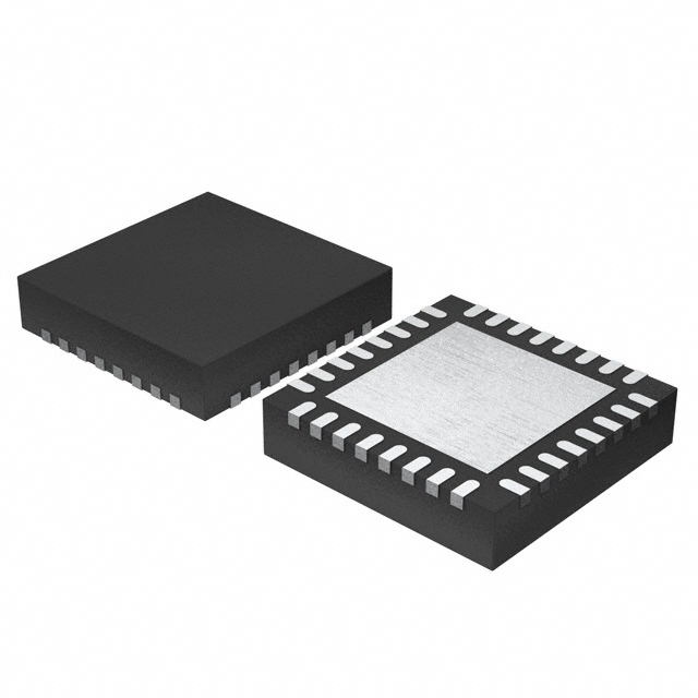


 工商网监
湘ICP备2023018690号
工商网监
湘ICP备2023018690号

