MCP2030
Three-Channel Analog Front-End Device
Device Features:
Description:
•
•
•
•
The MCP2030 is a stand-alone Analog Front-End
(AFE) device for Low-Frequency (LF) sensing and bidirectional communication applications. The device has
eight internal Configuration registers which are
readable and programmable, except the read-only
STATUS register, by an external device.
•
•
•
•
•
•
•
•
•
•
•
Three input pins for analog input signals
High input detection sensitivity (3 mVPP, typical)
High modulation depth sensitivity (as low as 8%)
Three output selections:
- Demodulated data
- Carrier clock
- RSSI
Input carrier frequency: 125 kHz, typical
Input data rate: 10 Kbps, maximum
8 internal Configuration registers
Bidirectional transponder communication
(LF talk back)
Programmable antenna tuning capacitance
(up to 63 pF, 1 pF/step)
Programmable output enable filter
Low standby current: 4 A (with 3 channels
enabled), typical
Low operating current: 13 A (with 3 channels
enabled), typical
Serial Peripheral Interface (SPI™) with external
devices
Supports Battery Back-Up mode and batteryless
operation with external circuits
Industrial and Extended Temperature Range:
-40°C to +85°C (industrial)
Typical Applications:
• Automotive industry applications:
- Passive Keyless Entry (PKE) transponder
- Remote door locks and gate openers
- Engine immobilizer
- LF initiator sensor for tire pressure monitoring
systems
• Security Industry applications:
- Long range access control transponder
- Parking lot entry transponder
- Hands-free apartment door access
- Asset control and management
The device has three low-frequency input channels.
Each input channel can be individually enabled or disabled. The device can detect an input signal with amplitude as low as ~1 mVPP and can demodulate an
amplitude-modulated input signal with as low as 8%
modulation depth. The device can also transmit data by
clamping and unclamping the input LC antenna
voltage.
The device can output demodulated data, carrier clock
or RSSI current depending on the register setting. The
demodulated data and carrier clock outputs are available on the LFDATA pin, while the RSSI output is available on the RSSI pin. The RSSI current output is
linearly proportional to the input signal strength.
The device has programmable internal tuning capacitors for each input channel. The user can program
these capacitors up to 63 pF, 1 pF per step. These
internal tuning capacitors can be used effectively for
fine-tuning of the external LC resonant circuit.
The device is optimized for very low current consumption and has various battery-saving low-power modes
(Sleep, Standby, Active). The device can also be operated in Battery Back-up and Batteryless modes using a
few external components.
This device is available in 14-pin PDIP, SOIC, and
TSSOP packages. This device is also used as the AFE
in the PIC16F639.
Package Types:
MCP2030
PDIP, SOIC, TSSOP
VSS
1
14
VSS
LCCOM
CS
2
13
SCLK/ALERT
3
RSSI
4
12 NC
LCX
11
LFDATA/
CCLK/SDIO
VDD
2005-2013 Microchip Technology Inc.
NC 5
10
LCY
6
9
LCZ
7
8
VDD
DS21981B-page 1
�MCP2030
NOTES:
DS21981B-page 2
2005-2013 Microchip Technology Inc.
�MCP2030
1.0
ELECTRICAL SPECIFICATIONS
Absolute Maximum Ratings(†)
Ambient temperature under bias...................-40°C to +125°C
† Notice: Stresses above those listed under “Maximum
Ratings” may cause permanent damage to the device. This is
a stress rating only and functional operation of the device at
those or any other conditions above those indicated in the
operation listings of this specification is not implied. Exposure
to maximum rating conditions for extended periods may affect
device reliability.
Storage temperature .................................... -65°C to +150°C
Voltage on VDD with respect to VSS ............... -0.3V to +6.5V
Voltage on all other pins with
respect to VSS ...................................... -0.3V to (VDD + 0.3V)
Maximum current out of VSS pin .................................300 mA
Maximum current into VDD pin ....................................250 mA
Maximum LC Input Voltage
(LCX, LCY, LCZ) loaded, with device........................ 10.0 VPP
Maximum LC Input Voltage
(LCX, LCY, LCZ) unloaded, without device............. 700.0 VPP
Maximum Input Current (rms) into device
per LC Channel.............................................................10 mA
Human Body ESD rating ....................................2000 (min.) V
Machine Model ESD rating ..................................200 (min.) V
DC Characteristics
Electrical Specifications: Standard Operating Conditions (unless otherwise stated)
Operating temperature
-40C TA +85C
LC Signal Input
Sinusoidal 300 mVPP
Carrier Frequency
125 kHz
LCCOM connected to VSS
Sym.
Min.
Typ†
Max.
Units
Supply Voltage
Parameters
VDD
2.0
3.0
3.6
V
VDD Start Voltage to ensure internal
Power-on Reset signal
VPOR
—
—
1.8
V
Modulation Transistor-on Resistance
RM
—
50
100
Active Current (detecting signal)
1 LC Input Channel Receiving Signal
3 LC Input Channel Receiving Signals
IACT
—
—
10
13
—
18
A
A
Standby Current (wait to detect signal)
1 LC Input Channel Enabled
2 LC Input Channels Enabled
3 LC Input Channels Enabled
ISTDBY
—
—
—
2
3
4
5
6
7
A
A
A
Sleep Current
ISLEEP
—
0.2
1
A
—
—
—
—
1
1
A
A
Analog Input Leakage Current
LCX, LCY, LCZ
LCCOM
IAIL
Conditions
VDD = 3.0V
CS = VDD
Input = Continuous Wave (CW);
Amplitude = 300 mVPP.
All channels enabled.
CS = VDD; ALERT = VDD
CS = VDD; ALERT = VDD
VDD = 3.6V, VSS VIN 1V with respect to
ground. Internal tuning capacitors are switched
off, tested in Sleep mode.
Digital Input Low Voltage
VIL
VSS
—
0.3 VDD
V
SCLK, SDI, CS
Digital Input High Voltage
VIH
0.8 VDD
—
VDD
V
SCLK, SDI, CS
Digital Input Leakage Current (Note 1)
SDI
SCLK, CS
IIL
—
—
—
—
1
1
A
A
—
—
VSS +0.4
V
Digital Output Low Voltage
ALERT, LFDATA/SDIO
VOL
Digital Output High Voltage
ALERT, LFDATA/SDIO
VOH
Digital Input Pull-Up Resistor
CS, SCLK
RPU
Note
*
†
1:
VDD - 0.5
—
—
V
50
200
350
k
VDD = 3.6V
VSS VPIN VDD
VPIN VDD
Analog Front-End section
IOL = 1.0 mA, VDD = 2.0V
IOH = -400 A, VDD = 2.0V
VDD = 3.6V
These parameters are characterized but not tested.
Data in “Typ” column is at 3.0V, +25C unless otherwise stated. These parameters are for design guidance only and are not tested.
Negative current is defined as current sourced by the pin.
2005-2013 Microchip Technology Inc.
DS21981B-page 3
�MCP2030
AC Characteristics
Electrical Specifications: Standard Operating Conditions (unless otherwise stated)
Supply Voltage
2.0V VDD 3.6V
Operating temperature
-40°C TA +85°C
LCCOM connected to VSS
LC Signal Input
Sinusoidal 300 mVPP
Carrier Frequency
125 kHz
LCCOM connected to VSS
Parameters
Input Sensitivity
Sym.
Min.
Typ†
Max.
Units
VSENSE
1
3.0
6
mVPP
Conditions
VDD = 3.0V
Output enable filter disabled
AGCSIG = 0; MODMIN = 00
(33% modulation depth setting)
Input = Continuous Wave (CW)
Output = Logic level transition from
low-to-high at sensitivity level for CW input.
Coil de-Q’ing Voltage RF Limiter (RFLM) must be active
VDE_Q
3
—
5
V
VDD = 3.0V, Force IIN = 5 A (worst case)
RF Limiter Turn-on Resistance
(LCX, LCY, LCZ)
RFLM
—
300
700
VDD = 2.0V, VIN = 8 VDC
Sensitivity Reduction
SADJ
—
—
0
-30
—
—
dB
dB
—
—
—
60
33
14
8
84
49
26
%
%
%
%
Minimum Modulation Depth
60% setting
33% setting
14% setting
8%
VIN_MOD
Carrier frequency
FCARRIER
—
125
—
kHz
Input modulation frequency
FMOD
—
—
10
kHz
LCX Tuning Capacitor
CTUNX
—
0
—
pF
44
59
82
pF
—
0
—
pF
44
59
82
pF
—
0
—
pF
44
59
82
pF
LCY Tuning Capacitor
LCZ Tuning Capacitor
CTUNY
CTUNZ
Q of Internal Tuning Capacitors
Q_C
50 *
—
—
Demodulator Charge Time
(delay time of demodulated output to rise)
TDR
—
50
—
Note
*
†
1:
2:
s
VDD = 3.0V
No sensitivity reduction selected
Max. reduction selected
Monotonic increment in attenuation value
from setting = 0000 to 1111 by design
VDD = 3.0V
See Section 5.21 “Minimum Modulation
Depth Requirement for Input Signal”.
See Modulation Depth Definition in
Figure 5-5.
Input data rate with NRZ data format.
VDD = 3.0V
Minimum modulation depth setting = 33%
Input conditions:
Amplitude = 300 mVPP
Modulation depth = 100%
VDD = 3.0V,
Config. Reg. 1, bits Setting = 000000
63 pF ±30%
Config. Reg. 1, bits Setting = 111111
63 steps, approx. 1 pF/step
Monotonic increment in capacitor value from
setting = 000000 to 111111 by design
VDD = 3.0V,
Config. Reg. 2, bits Setting = 000000
63 pF ±30%
Config. Reg. 2, bits Setting = 111111
63 steps, approx. 1 pF/step
Monotonic increment in capacitor value from
setting = 000000 to 111111 by design
VDD = 3.0V,
Config. Reg. 3, bits Setting = 000000
63 pF ±30%
Config. Reg. 3, bits Setting = 111111
63 steps, approx. 1 pF/step
Monotonic increment in capacitor value from
setting = 000000 to 111111 by design
VDD = 3.0V
Minimum modulation depth setting = 33%
Input conditions:
Amplitude = 300 mVPP
Modulation depth = 100%
Parameter is characterized but not tested.
Data in “Typ” column is at 3.0V, 25°C unless otherwise stated. These parameters are for design guidance only and are not tested.
Required output enable filter high time must account for input path analog delays (= TOEH - TDR + TDF).
Required output enable filter low time must account for input path analog delays (= TOEL + TDR - TDF).
DS21981B-page 4
2005-2013 Microchip Technology Inc.
�MCP2030
AC Characteristics (Continued)
Electrical Specifications: Standard Operating Conditions (unless otherwise stated)
Supply Voltage
2.0V VDD 3.6V
Operating temperature
-40°C TA +85°C
LCCOM connected to VSS
LC Signal Input
Sinusoidal 300 mVPP
Carrier Frequency
125 kHz
LCCOM connected to VSS
Parameters
Sym.
Min.
Typ†
Max.
Units
Demodulator Discharge Time (delay time
of demodulated output to fall)
TDF
—
50
—
s
Rise time of LFDATA
TRLFDATA
—
0.5
—
s
VDD 3.0V. Time is measured from 10% to
90% of amplitude
Fall time of LFDATA
TFLFDATA
—
0.5
—
s
VDD 3.0V
Time is measured from 10% to 90% of
amplitude
TSTAB
4
—
—
ms
ms
AGC stabilization time
(TAGC + TPAGC)
AGC initialization time
TAGC
—
3.5
—
High time after AGC initialization time
TPAGC
—
62.5
—
Gap time after AGC stabilization time
TGAP
200
—
—
Conditions
VDD = 3.0V
MOD depth setting = 33%
Input conditions:
Amplitude = 300 mVPP
Modulation depth = 100%
TE
100
—
—
s
s
s
Time from exiting Sleep or POR to being
ready to receive signal
TRDY
—
—
50*
ms
Minimum time AGC level must be held
after receiving AGC Preserve command
TPRES
5*
—
—
ms
AGC level must not change more than 10%
during TPRES.
Internal clock trimmed at 32 kHz during test
Time element of pulse
Internal RC oscillator frequency
Minimum pulse width
FOSC
27
32
35.5
kHz
Inactivity timer time-out
TINACT
13.5
16
17.75
ms
512 cycles of RC oscillator @ FOSC
Alarm timer time-out
TALARM
27
32
35.5
ms
1024 cycles of RC oscillator @ FOSC
—
800*
—
k
LCCOM grounded, VDD = 3V,
FCARRIER = 125 kHz.
—
24*
—
pF
LCCOM grounded, VDD = 3V,
FCARRIER = 125 kHz.
LC Pin Input Resistance for
LCX, LCY, LCZ pins
RIN
LC Pin Input Parasitic Capacitance for
LCX, LCY, LCZ pins
CIN
Minimum output enable filter high time
OEH (Bits Config0)
01 = 1 ms
10 = 2 ms
11 = 4 ms
00 = Filter Disabled
TOEH
Minimum output enable filter low time
OEL (Bits Config0)
00 = 1 ms
01 = 1 ms
10 = 2 ms
11 = 4 ms
TOEL
Maximum output enable filter period
TOET
32 (~1 ms)
64 (~2 ms)
128 (~4 ms)
—
32 (~1 ms)
32 (~1 ms)
64 (~2 ms)
128 (~4 ms)
—
—
—
—
—
—
—
—
—
—
—
—
—
—
—
—
clock
count
clock
count
RC oscillator = FOSC (see FOSC specification
for variations).
Viewed from the pin input:
(Note 1)
RC oscillator = FOSC
Viewed from the pin input:
(Note 2)
RC oscillator = FOSC
OEH
01
01
01
01
OEL
00
01
10
11
=
=
=
=
TOEH
1 ms
1 ms
1 ms
1 ms
TOEL
1 ms
1 ms
2 ms
4 ms
(Filter 1)
(Filter 1)
(Filter 2)
(Filter 3)
—
—
—
—
—
—
—
—
96 (~3 ms)
96 (~3 ms)
128 (~4 ms)
192 (~6 ms)
10
10
10
10
00
01
10
11
=
=
=
=
2 ms
2 ms
2 ms
2 ms
1 ms
1 ms
2 ms
4 ms
(Filter 4)
(Filter 4)
(Filter 5)
(Filter 6)
—
—
—
—
—
—
—
—
128 (~4 ms)
128 (~4 ms)
160 (~5 ms)
250 (~8 ms)
11
11
11
11
00
01
10
11
=
=
=
=
4 ms
4 ms
4 ms
4 ms
1 ms
1 ms
2 ms
4 ms
(Filter 7)
(Filter 7)
(Filter 8)
(Filter 9)
—
—
—
—
—
—
—
—
192 (~6 ms)
192 (~6 ms)
256 (~8 ms)
320 (~10 ms)
00
XX
= Filter Disabled
—
—
—
*
†
1:
2:
Parameter is characterized but not tested.
Data in “Typ” column is at 3.0V, 25°C unless otherwise stated. These parameters are for design guidance only and are not tested.
Required output enable filter high time must account for input path analog delays (= TOEH - TDR + TDF).
Required output enable filter low time must account for input path analog delays (= TOEL + TDR - TDF).
Note
2005-2013 Microchip Technology Inc.
clock
count
LFDATA output appears as long as input
signal level is greater than VSENSE.
DS21981B-page 5
�MCP2030
AC Characteristics (Continued)
Electrical Specifications: Standard Operating Conditions (unless otherwise stated)
Supply Voltage
2.0V VDD 3.6V
Operating temperature
-40°C TA +85°C
LCCOM connected to VSS
LC Signal Input
Sinusoidal 300 mVPP
Carrier Frequency
125 kHz
LCCOM connected to VSS
Parameters
RSSI current output
RSSI current linearity
Note
*
†
1:
2:
Sym.
Min.
Typ†
Max.
Units
IRSSI
—
6
—
0.65
12
100
2
20.3
—
A
A
A
ILRRSSI
-15
—
15
%
Conditions
VIN = 37 mVPP
VIN = 370 mVPP
VDD = 3.0V, VIN = 0 to 4 VPP
Linearly increases with input signal amplitude.
Tested at VIN = 37 mVPP, 100 mVPP, and
370 mVPP at +25ºC.
Tested at room temperature only (see
Equation 5-1 and Figure 5-7 for test method).
Parameter is characterized but not tested.
Data in “Typ” column is at 3.0V, 25°C unless otherwise stated. These parameters are for design guidance only and are not tested.
Required output enable filter high time must account for input path analog delays (= TOEH - TDR + TDF).
Required output enable filter low time must account for input path analog delays (= TOEL + TDR - TDF).
SPI Timing
Electrical Specifications: Standard Operating Conditions (unless otherwise stated)
Supply Voltage
2.0V VDD 3.6V
Operating temperature
-40°C TA +85°C
LC Signal Input
Sinusoidal 300 mVPP
Carrier Frequency
125 kHz
LCCOM connected to VSS
Parameters
Sym.
Min.
Typ†
Max.
Units
SCLK Frequency
FSCLK
—
—
3
MHz
CS fall to first SCLK edge setup time
TCSSC
100
—
—
ns
SDI setup time
TSU
30
—
—
ns
SDI hold time
THD
50
—
—
ns
SCLK high time
THI
150
—
—
ns
SCLK low time
TLO
150
—
—
ns
SDO setup time
Conditions
TDO
—
—
150
ns
SCLK last edge to CS rise setup time
TSCCS
100
—
—
ns
CS high time
TCSH
500
—
—
ns
CS rise to SCLK edge setup time
TCS1
50
—
—
ns
SCLK edge to CS fall setup time
TCS0
50
—
—
ns
SCLK edge when CS is high
Rise time of SPI data
(SPI Read command)
TRSPI
—
10
—
ns
VDD 3.0V. Time is measured from 10% to
90% of amplitude
Fall time of SPI data
(SPI Read command)
TFSPI
—
10
—
ns
VDD 3.0V. Time is measured from 90% to
10% of amplitude
†
Data in “Typ” column is at 3.0V, 25°C unless otherwise stated. These parameters are for design guidance only and are not tested.
DS21981B-page 6
2005-2013 Microchip Technology Inc.
�MCP2030
2.0
TYPICAL PERFORMANCE CURVES
Note:
The graphs and tables provided following this note are a statistical summary based on a limited number of
samples and are provided for informational purposes only. The performance characteristics listed herein
are not tested or guaranteed. In some graphs or tables, the data presented may be outside the specified
operating range (e.g., outside specified power supply range) and therefore outside the warranted range.
Standby Current (1 Channel Enabled)
Active Current (1 Channel Enabled)
+85C
+25C
-40C
2
1.5
1
0.5
9
8
7
6
5
4
3
2
1
0
Current Draw (A)
Current Draw (A)
2.5
0
2V
3V
+85C
+25C
-40C
2V
3.6 V
VDD (V)
12
+85C
+25C
3
-40C
2.5
2
1.5
1
0.5
Current Draw (A)
Current Draw (A)
4
3.5
3.6 V
Active Current (2 Channels Enabled)
Standby Current (2 Channels Enabled)
+85C
+25C
-40C
10
8
6
4
2
0
0
2V
3V
3.6 V
2V
+85C
+25C
-40C
3
2
1
0
2V
3V
Current Draw (A)
6
4
16
14
12
10
8
6
4
2
0
3.6 V
Typical Standby Current.
2005-2013 Microchip Technology Inc.
+85C
+25C
-40C
2V
VDD (V)
FIGURE 2-1:
3.6 V
Active Current (3 Channels Enabled)
Standby Current (3 Channels Enabled)
5
3V
VDD (V)
VDD (V)
Current Draw (A)
3V
VDD (V)
3V
3.6 V
VDD (V)
FIGURE 2-2:
Typical Active Current.
DS21981B-page 7
�12
35
De-Q'ed (Loaded) Coil Voltage
(V PP)
Oscillator Frequency (kHz.)
MCP2030
34
33
Osc. Freq. @ VDD = 3.6V
32
31
Osc. Freq. @ VDD = 2.0V
30
29
-50
-25
0
25
50
75
100
10
8
6
4
2
0
0
125
200
400
600
Unloaded Coil Voltage (VPP)
Temperature (°C)
50.0%
45.0%
40.0%
FIGURE 2-6:
De-Q’ed Voltage vs.
Unloaded Coil Voltage.
VDD = 2.0V
80
-40C
25C
85C
70
60
Ohms
35.0%
30.0%
25.0%
20.0%
15.0%
10.0%
5.0%
0.0%
Ch. X
Ch. Y
Ch. Z
50
40
30
20
10
35
34
33
32
31
30
29
28
0
27
Percentage of Occurences (%)
FIGURE 2-3:
Oscillator Frequency vs.
Temperature, VDD = 3.6V and 2.0V.
0
2
FIGURE 2-4:
Oscillator Frequency
Histograms vs. Temperature, VDD = 2V.
VDD = 3.6V
6
FIGURE 2-7:
Modulation Transistor-on
Resistance (+25°C).
25
-40C
25C
85C
20
15
10
5
0
200
400
600
F re que nc y ( k H z)
35
34
33
32
31
30
29
28
0
27
Percentage of Occurences (%)
4
VDD (V)
Oscillator Frequency (kHz.)
50.0%
45.0%
40.0%
35.0%
30.0%
25.0%
20.0%
15.0%
10.0%
5.0%
0.0%
800
Oscillator Frequency (kHz.)
FIGURE 2-5:
Oscillator Frequency
Histograms vs. Temperature at VDD = 3V.
DS21981B-page 8
FIGURE 2-8:
Bandwidth.
Channel Sensitivity vs.
2005-2013 Microchip Technology Inc.
�MCP2030
70
120
60
+25°C
+85°C
80
Capacitance (pF)
RSSI (µA)
100
-40°C
60
40
20
50
Ch. X
Ch. Y
Ch. Z
40
30
20
10
0
6
5
5.5
4
4.5
3
3.5
2
2.5
1
1.5
0.5
0
0
0
Input Voltage (V)
40
60
80
Bit Setting (steps)
FIGURE 2-9:
Typical RSSI Output Current
vs. Input Signal Strength.
FIGURE 2-11:
Typical Tuned Capacitance
Value vs. Configuration Register Bit Setting
(VDD = 3V,Temperature = -40°C.
70
70
60
60
50
Ch. X
Ch. Y
Ch. Z
40
30
20
10
Capacitance (pF)
Capacitance (pF)
20
50
Ch. X
Ch. Y
Ch. Z
40
30
20
10
0
0
0
20
40
60
80
0
20
40
60
80
Bit Setting (Steps)
Bit Setting (Steps)
FIGURE 2-10:
Typical Tuned Capacitance
Value vs. Configuration Register Bit Setting
(VDD = 3V, Temperature = +25°C.
FIGURE 2-12:
Typical Tuned Capacitance
Value vs. Configuration Register Bit Setting
(VDD = 3V,Temperature = +85°C.
2005-2013 Microchip Technology Inc.
DS21981B-page 9
�MCP2030
80
60
50
Ch-X
Ch-Y
Ch-Z
40
30
TDR (µs)
RSSI Current (A)
70
20
10
0
0
2
4
6
100
90
80
70
60
50
40
30
20
10
0
8%
14%
33%
60%
85C
8
Input Voltage (V)
-20C
-40C
FIGURE 2-14:
Example of Typical TDR
Changes over Temperature.
Input Signal Condition: Amplitude = 300 mVPP,
Modulation Depth = 100 %.
Device (a)
80
70
60
50
60
Ch-X
Ch-Y
Ch-Z
40
30
20
50
TDF (µs)
RSSI Current (A)
25C
Temperature (°C)
10
0
60%
40
30
33%
20
0
2
4
6
14%
8
10
Input Voltage (V)
8%
0
Device (b)
85C
25C
-20C
-40C
Temperature (°C)
80
Current (A)
70
60
50
Ch-X
Ch-Y
Ch-Z
40
30
FIGURE 2-15:
Example of Typical TDF
Changes over Temperature.
Input Signal Condition: Amplitude = 300 mVPP,
Modulation Depth = 100 %.
20
10
0
0
2
4
6
8
Input Voltage (V)
Device (c)
Note:
Equal amplitude is applied to each channel.
FIGURE 2-13:
Examples of RSSI Output
Current Variations Between Channel to Channel
and Device to Device at Room Temperature.
DS21981B-page 10
2005-2013 Microchip Technology Inc.
�MCP2030
2.1
Performance Plots
(a) Sensitivity = 1.06 mVPP
Demodulated output
Input signal
(b) Sensitivity = 3 mVPP
Demodulated output
Input signal
FIGURE 2-16:
Input Sensitivity Example.
2005-2013 Microchip Technology Inc.
DS21981B-page 11
�MCP2030
Note:
FIGURE 2-17:
DS21981B-page 12
Ch2 is the input and Ch1 is the output (demodulated data appears after AGC Initialization time (TAGC)).
Output Enable Filter is disabled.
Typical AGC Initialization Time at Room Temperature (VDD = 3V).
2005-2013 Microchip Technology Inc.
�MCP2030
Note:
FIGURE 2-18:
Ch3 is the input with correct Output Enable Filter timing.
Ch1 is the demodulated LFDATA output.
Ch2 is the ALERT pin output. It shows that the ALERT output pin maintains logic high if the input signal
meets the programmed filter timing requirement.
ALERT Output Example: With No Parity Error and no 32 ms Alarm Timer Time-out.
2005-2013 Microchip Technology Inc.
DS21981B-page 13
�MCP2030
Note:
The 32 ms Alarm Timer is enabled only if the Output Enable Filter is enabled.
Ch3 is the input signal with incorrect Output Enable Filter timing.
Ch1 is the demodulated LFDATA output. No output since the input filter is not matched.
Ch2 is the ALERT output.
The output shows that the logic level changes after 32 ms from the AGC initialization time (TAGC) if the input
signal does not meet the programmed filter timing requirement.
FIGURE 2-19:
DS21981B-page 14
ALERT Output Example: With 32 ms Alarm Timer Timed out.
2005-2013 Microchip Technology Inc.
�MCP2030
(a) Output (Ch 1):
Device repeats
Soft Reset after
16 ms inactivity
timer has timed out
(b) Input (Ch 2):
Input has no
modulation
Note:
Ch 2 is the input without modulation (i.e., noise)
Ch 1 is the output at the LFDATA pin due to the 16 ms Soft Inactivity Timer timed out. Note the 3.5 ms AGC
initialization time after the Soft Reset.
The cases shown above apply when the Output Filter is disabled.
FIGURE 2-20:
Examples of Soft Inactivity Timer Timed out: This output is available only if the Output
Enable Filter is disabled.
2005-2013 Microchip Technology Inc.
DS21981B-page 15
�MCP2030
Coil Voltage
LCX
Clock Pulses
SCLK
Clamp On
Command
SDI
Coil Voltage
LCX
Clock Pulses
SCLK
Clamp Off
Command
SDI
FIGURE 2-21:
DS21981B-page 16
Examples of Clamp-On and Clamp-Off Commands and Changes in Coil Voltage.
2005-2013 Microchip Technology Inc.
�MCP2030
Demodulated output
Input signal with 77%
modulation depth
FIGURE 2-22:
Example of Minimum Modulation Depth Setting: Modulation Depth of Input Signal =
77%, Minimum Modulation Depth (MODMIN) Setting = 60%.
Demodulated output
Input signal with 56%
modulation depth
Note:
There is no demodulated output since the modulation depth of the input signal is lower than the minimum
modulation depth setting. The device will have demodulated output if the Minimum Modulation Depth option
is set to 8%, 14%, or 33%.
FIGURE 2-23:
Example of Minimum Modulation Depth Setting: Modulation Depth of Input
Signal = 56%, Minimum Modulation Depth (MODMIN) Setting = 60%.
2005-2013 Microchip Technology Inc.
DS21981B-page 17
�MCP2030
Demodulated output
Input signal with 42%
modulation depth
FIGURE 2-24:
Example of Minimum Modulation Depth Setting: Modulation Depth of Input Signal =
42%, Minimum Modulation Depth (MODMIN) Setting = 33%.
Demodulated output
Input signal with 14%
modulation depth
FIGURE 2-25:
Example of Minimum Modulation Depth Setting: Modulation Depth of Input Signal =
14%, Minimum Modulation Depth (MODMIN) Setting = 14%.
DS21981B-page 18
2005-2013 Microchip Technology Inc.
�MCP2030
Filter 1
Output Enable
Filter Timing of
Input Signal
TOEH = 1 ms
TOEL = 1 ms
TOET = 3 ms
Configuration
Bit Settings
OEH
OEL
01
00
01
01
or
Filter 2
Output Enable
Filter Timing of
Input Signal
TOEH = 1 ms
TOEL = 2 ms
TOET = 4 ms
Configuration
Bit Settings
OEH
OEL
01
10
Filter 3
Output Enable
Filter Timing of
Input Signal
TOEH = 1 ms
TOEL = 4 ms
TOET = 6 ms
FIGURE 2-26:
Outputs.
Configuration Bit
Settings
OEH
OEL
01
11
Examples of Output Enable Filters 1 through 3 (Wake-up Filters) and Demodulated
2005-2013 Microchip Technology Inc.
DS21981B-page 19
�MCP2030
Filter 4
Output Enable
Filter Timing of
Input Signal
TOEH = 2 ms
TOEL = 1 ms
TOET = 4 ms
Configuration Bit
Settings
OEH
OEL
10
00
10
01
or
Filter 5
Output Enable
Filter Timing of
Input Signal
TOEH = 2 ms
TOEL = 2 ms
TOET = 5 ms
Configuration Bit
Settings
OEH
OEL
10
10
Filter 6
Output Enable
Filter Timing of
Input Signal
TOEH = 2 ms
TOEL = 4 ms
TOET = 8 ms
FIGURE 2-27:
Outputs.
DS21981B-page 20
Configuration
Bit Settings
OEH
OEL
10
11
Examples of Output Enable Filters 4 through 6 (Wake-up Filters) and Demodulated
2005-2013 Microchip Technology Inc.
�MCP2030
Filter 7
Output Enable
Filter Timing of
Input Signal
TOEH = 4 ms
TOEL = 1 ms
TOET = 6 ms
Configuration Bit
Settings
OEH
OEL
11
00
11
01
or
Filter 8
Output Enable
Filter Timing of
Input Signal
TOEH = 4 ms
TOEL = 2 ms
TOET = 8 ms
Configuration
Bit Settings
OEH
OEL
11
10
Filter 9
Output Enable
Filter Timing of
Input Signal
TOEH = 4 ms
TOEL = 4 ms
TOET = 10 ms
FIGURE 2-28:
Outputs.
Configuration Bit
Settings
OEH
OEL
11
11
Examples of Output Enable Filters 7 through 9 (Wake-up Filters) and Demodulated
2005-2013 Microchip Technology Inc.
DS21981B-page 21
�MCP2030
LFDATA
Output
Input Signal
Note:
Demodulated output is available immediately after AGC initialization.
FIGURE 2-29:
Input Signal and Demodulated Output When the Output Enable Filter is Disabled.
LFDATA
Output
Input Signal
Note:
Demodulated output is available only if the incoming signal meets the enable filter timing criteria that is defined in the
Configuration Register 0 (Register 5-1). If the criteria is met, the output is available after the low timing (TOEL) of the
Enable Filter.
FIGURE 2-30:
Input Signal and Demodulator Output When Output Enable Filter is Enabled and Input
Meets Filter Timing Requirements.
DS21981B-page 22
2005-2013 Microchip Technology Inc.
�MCP2030
No LFDATA
Output
Input Signal
FIGURE 2-31:
No Demodulator Output When Output Enable Filter is Enabled But Input Does Not
Meet Filter Timing Requirements.
2005-2013 Microchip Technology Inc.
DS21981B-page 23
�MCP2030
Carrier Clock Output
Carrier Input
(a) Carrier Clock Output with Carrier/1 Option
Carrier Clock Output
Carrier Input
(b) Carrier Clock Output with Carrier/4 Option
FIGURE 2-32:
DS21981B-page 24
Carrier Clock Output Examples.
2005-2013 Microchip Technology Inc.
�MCP2030
3.0
PIN DESCRIPTIONS
TABLE 3-1:
PIN FUNCTION TABLES
Pin No.
Symbol
I/O/P
1
VSS
P
Function
Ground Pin.
Chip Select Digital Input Pin.
2
CS
I
3
SCLK/ALERT
I/O
Clock input for the modified 3-wire SPI interface.
ALERT output: This pin goes low if there is a parity error in the
Configuration register or the 32 ms alarm timer is timed out.
4
RSSI
O
Received Signal Strength Indicator (RSSI) current output.
5
NC
N/A
No Connect.
6
LFDATA/CCLK/SDIO
I/O
Demodulated data output.
Carrier clock output.
Serial input or output data for the modified 3-wire SPI interface.
7
VDD
P
Positive Supply Voltage Pin.
8
VDD
P
Positive Supply Voltage Pin.
9
LCZ
I
Input pin for external LC antennas.
10
LCY
I
Input pin for external LC antennas.
Input pin for external LC antennas.
11
LCX
I
12
NC
N/A
13
LCCOM
I
Common reference input for the external LC antennas.
14
VSS
P
Ground Pin.
No Connect.
Type Identification: I = Input; O = Output; P = Power
3.1
Supply Voltage (VDD, VSS)
The VDD pin is the power supply pin for the analog and
digital circuitry within the MCP2030. This pin requires
an appropriate bypass capacitor of 0.1 µF. The voltage
on this pin should be maintained in the 2.0V-3.6V range
for specified operation.
The VSS pin is the ground pin and the current return
path for both analog and digital circuitry of the
MCP2030. If an analog ground plane is available, it is
recommended that this device be tied to the analog
ground plane of the PCB.
3.2
Chip Select (CS)
The CS pin needs to stay high when the device is
receiving input signals. Leaving the CS pin low will
place the device in the SPI Programming mode.
3.3
SPI Clock Input (SCLK/ALERT)
This pin becomes the SPI clock input (SCLK) when CS
is low, and becomes the ALERT output when CS is
high.
The ALERT pin is an open collector output. This pin has
an internal pull-up resistor to ensure that no spurious
SPI communication occurs between power-up and pin
configuration of the MCU.
3.4
Received Signal Strength
Indicator (RSSI)
This pin becomes the Received Signal Strength Indicator
(RSSI) output current sink when the RSSI output option
is selected.
The CS pin is an open collector output. This pin has an
internal pull-up resistor to ensure that no spurious SPI
communication occurs between power-up and pin
configuration of the MCU.
2005-2013 Microchip Technology Inc.
DS21981B-page 25
�MCP2030
3.5
Demodulated Data Output (LFDATA)
Carrier Clock Output (CCLK)
SPI Data I/O (SDIO)
When the CS pin is high, this pin is an output pin for
demodulated data or carrier clock depending on output
type selection. When carrier clock output (CCLK) is
selected, the LFDATA output is a square pulse of the
input carrier clock and is available as soon as the AGC
stabilization time (TSTAB) is completed.
When the CS pin is low, this pin becomes the SPI data
input and output (SDIO).
3.6
LC Input (LCX, LCY, LCZ)
These pins are the input pins for the external LC
resonant antenna circuits. The antenna circuits are
connected between the LC pin and the LCCOM pin.
3.7
LC Common Reference (LCCOM)
This pin is the common reference input pin for the
external LC resonant circuit.
DS21981B-page 26
2005-2013 Microchip Technology Inc.
�MCP2030
4.0
APPLICATION INFORMATION
4.1
The MCP2030 is a stand-alone 3-channel analog
front-end device for low frequency (LF) sensing and
bidirectional transponder applications. By connecting
three orthogonally placed LC resonant antennas to
the LC input pins, it can detect signals from all
directions (x, y and z).
Battery Back-up and Batteryless
Operation
The device supports both battery back-up and
batteryless operation by the addition of external
components, allowing the device to be partially or
completely powered from the field.
Figure 4-1 shows an example of the external circuit for
the battery back-up.
The device draws more current when all channels are
enabled as compared to a single channel; therefore, it
is recommended to disable any unused channels by
setting Configuration Register 0 (Register 5-1).
Note:
Voltage on LCCOM combined with coil
input voltage must not exceed the maximum LC input voltage.
The device’s high input sensitivity (as low as 1 mVPP)
and ability to detect weakly modulated (as low as 8%)
input signals with its low power feature set, makes the
device suitable for various applications such as a lowcost hands-free Passive Keyless Entry (PKE)
transponder, an LF Initiator sensor for Tire Pressure
Monitoring Systems (TPMS) and long-range access
control applications in the automotive and security
industries.
VDD
VBAT
RLIM
LCX
DFLAT1
DBLOCK
DLIM
CPOOL
LX
LCY
CX
Air Coil
LY
LCZ
CY
LZ
CZ
LCCOM
DFLAT2
RCOM
Legend:
CCOM
CCOM = LCCOM charging capacitor.
CPOOL = Pool capacitor (or battery back-up capacitor), charges in field and powers device.
DBLOCK = Battery protection from reverse charge.
Schottky for low forward bias drop.
DFLAT = Field rectifier diodes.
DLIM = Voltage limiting diode, may be required to limit VDD voltage when in strong fields.
RCOM = LCCOM discharge path.
RLIM = Current limiting resistor, required for air coil in strong fields.
FIGURE 4-1:
External Circuit Example for LF Field Powering and Battery Back-up Mode.
2005-2013 Microchip Technology Inc.
DS21981B-page 27
�MCP2030
4.2
Application Examples
The output of the MCP2030 is fed into the external
MCU. The external MCU can send data by clamping on
and clamping off the MCP2030 coil voltages using an
SPI command, or via a UHF transmitter.
Figure 4-2 shows an example of an external circuit for
a bidirectional communication transponder application.
Each LC input pin is connected to an external LC
resonant circuit. To achieve the best performance, the
resonant frequency of the LC circuit needs to be
matched to the detecting carrier frequency of interest.
The resonant frequency is given by the following
equation:
The RSSI output of the MCP2030 can be digitized by
the MCU firmware. Users can also consider using a
MCU that has an internal analog-to-digital converter
(ADC) such as the PIC16F684 or a stand-alone ADC
device.
Figure 4-3 shows an example of a hands-free Passive
Keyless Entry (PKE) system. The base station unit
transmits an LF command. The MCP2030 detects the
base station command and feeds the detected output
to the external MCU (PIC16F636). If the command is
correct, the MCU responds via an external UHF
transmitter or by using the LF talk-back modulators of
the MCP2030 device.
1
f o = ------------------
2 LC
In typical 125 kHz applications, the L value is a few mH,
and the C value is a few hundred pF, for example,
L = 4.9 mH, and C = 331 pF.
The resonant frequency can be fine-tuned by programming the internal tuning capacitors.
Figure 4-4 shows an example when the device is used
for a tire pressure monitoring sensor application. The
device detects the LF Initiator commands and transmits
the tire pressure data to the base station via an external
UHF transmitter.
MCP2030
SW1
VSS
CS
SW2
SCLK/ALERT
SW3
PIC16F636/684
To ADC
SW4
VSS
LCCOM
NC
RSSI
LCX
NC
LCY
C
L
air-core
coil
C
ferrite-core
coil
L
C
L
LFDATA/CCLK/SDIO LCZ
+3V
VDD
VDD
+3V
ferrite-core coil
315/434 MHz
RF Circuitry
(UHF TX)
FIGURE 4-2:
DS21981B-page 28
Example of External Circuits for Bidirectional Communication Transponder Applications.
2005-2013 Microchip Technology Inc.
�MCP2030
d
Encrypte
Codes
se
Respon
F
(UH )
LED
LED
UHF
Transmitter
Ant. X
Ant. Y
LF
Transmitter/
Receiver
Ant. Z
MCU
(PIC16F636)
mand
LF Com z)
k
5
(12 H
MCP2030
(3D Stand Alone
Analog Front-End)
Microcontroller
(MCU)
UHF
Receiver
Response
(125 kHz)
PKE Transponder
Base Station
FIGURE 4-3:
Example of Bidirectional Hand-free Passive Keyless Entry (PKE) System.
UHF
tire respon
pres
s
sure e with
data
RF Receiver
MCU
RF Transmitter
MCU
Tire
Pressure
Sensor
Initiator
125 kHz
d
comman
LF Initiator
MCP2030
Note 1: The LF initiator sends LF commands to request the tire pressure data.
2: The MCP2030 picks up the LF commands and the MCU transmits the tire pressure data
via an external UHF transmitter.
FIGURE 4-4:
Example of Tire Pressure Monitoring Sensor Applications.
2005-2013 Microchip Technology Inc.
DS21981B-page 29
�MCP2030
NOTES:
DS21981B-page 30
2005-2013 Microchip Technology Inc.
�MCP2030
5.0
FUNCTIONAL DESCRIPTION
AND THEORY OF DEVICE
OPERATION
The MCP2030 contains three analog input channels for
signal detection and LF talk-back. This section
provides the function description of the device.
Each analog input channel has internal tuning
capacitors, sensitivity control circuits, an input signal
strength limiter and an LF talk-back modulation
transistor. An Automatic Gain Control (AGC) loop is
used for all three input channel gains. The output of
each channel is OR’d and fed into a demodulator. The
digital output is passed to the LFDATA pin. Figure 5-1
shows the block diagram of the device and Figure 5-2
shows the input signal path.
There are a total of eight Configuration registers. Six of
them are used for device operation options, one for
column parity bits and one for status indication of
device operation. Each register has 9 bits including one
row parity bit. These registers are readable and
writable by SPI commands except for the STATUS
register, which is read-only.
The device’s features are dynamically controllable by
programming the Configuration registers.
5.1
The modulation FET is also shorted momentarily after
Soft Reset and Inactivity timer time-out.
5.3
The signal levels from all 3 channels are combined
such that the limiter attenuates all 3 channels
uniformly, in respect to the channel with the strongest
signal.
Modulation Circuit
The modulation circuit consists of a modulation
transistor (FET), internal tuning capacitors and external
LC antenna components. The modulation transistor
and the internal tuning capacitors are connected
between the LC input pin and LCCOM pin. Each LC
input has its own modulation transistor.
When the modulation transistor turns on, its low Turnon Resistance (RM) clamps the induced LC antenna
voltage. The coil voltage is minimized when the
modulation transistor turns-on and maximized when
the modulation transistor turns-off. The modulation
transistor’s low turn-on resistance (RM) results in a high
modulation depth.
Tuning Capacitor
Each channel has internal tuning capacitors for external
antenna tuning. The capacitor values are programmed
by the Configuration registers up to 63 pF, 1 pF per step.
Note:
5.4
The user can control the tuning capacitor by programming the Configuration
registers. See Register 5-2 through
Register 5-4 for details.
Variable Attenuator
The variable attenuator is used to attenuate, via AGC
control, the input signal voltage to avoid saturating the
amplifiers and demodulators.
Note:
RF Limiter
The RF Limiter limits LC pin input voltage by de-Q’ing
the external LC resonant antenna circuit. The limiter
begins de-Q’ing the external LC antenna when the
input voltage exceeds VDE_Q, progressively de-Q’ing
harder to reduce the antenna input voltage.
5.2
The modulation data comes from the external microcontroller section via the digital SPI as “Clamp On”,
“Clamp Off” commands. Only those inputs that are
enabled will execute the Clamp command. A basic
block diagram of the modulation circuit is shown in
Figure 5-1 and Figure 5-2.
5.5
The variable attenuator function is
accomplished by the device itself. The
user cannot control its function.
Sensitivity Control
The sensitivity of each channel can be reduced by the
channel’s Configuration register sensitivity setting.
This is used to desensitize the channel from optimum.
Note:
5.6
The user can desensitize the channel
sensitivity
by
programming
the
Configuration registers. See Register 5-5
and Register 5-6 for details.
AGC Control
The AGC controls the variable attenuator to limit the
internal signal voltage to avoid saturation of internal
amplifiers and demodulators (Refer to Section 5.4
“Variable Attenuator”).
The signal levels from all 3 channels are combined
such that the AGC attenuates all 3 channels uniformly
in respect to the channel with the strongest signal.
Note:
The AGC control function is accomplished
by the device itself. The user cannot
control its function.
The LF talk-back is achieved by turning on and off the
modulation transistor.
2005-2013 Microchip Technology Inc.
DS21981B-page 31
�MCP2030
5.7
Fixed Gain Amplifiers 1 and 2
FGA1 and FGA2 provides a maximum two-stage gain
of 40 dB.
Note:
5.8
The user cannot control the gain of these
two amplifiers.
Auto-Channel Selection
The auto-channel selection feature is enabled if the
Auto-Channel Select bit AUTOCHSEL in Configuration Register 5 (Register 5-6) is set, and disabled if
the bit is cleared. When this feature is active (i.e.,
AUTOCHSE = 1), the control circuit checks the
demodulator output of each input channel immediately
after the AGC settling time (TSTAB). If the output is high,
it allows this channel to pass data, otherwise it is
blocked.
The status of this operation is monitored by STATUS
Register 7 bits (Register 5-8). These bits indicate
the current status of the channel selection activity, and
automatically updates for every Soft Reset period. The
auto-channel selection function resets after each Soft
Reset (or after Inactivity timer time-out). Therefore, the
blocked channels are re-enabled after Soft Reset.
This feature can make the output signal cleaner by
blocking any channel that was not high at the end of
TAGC. This function works only for demodulated data
output, and is not applied for carrier clock or RSSI
output.
5.9
Carrier Clock Detector
The Carrier Clock Detector senses the input carrier
cycles. The output of the detector switches digitally at
the signal carrier frequency. Carrier clock output is
available when the output is selected by the DATOUT
bit in Configuration Register 1 (Register 5-2).
5.10
Demodulator
The Demodulator consists of a full-wave rectifier, low
pass filter, peak detector and Data Slicer that detects
the envelope of the input signal.
5.11
Data Slicer
The Data Slicer consists of a reference generator and
comparator. The Data Slicer compares the input with
the reference voltage. The reference voltage comes
from the minimum modulation depth requirement
setting and input peak voltage. The data from all 3
channels are OR’d together and sent to the output
enable filter.
5.12
Output Enable Filter
The Output Enable Filter enables the LFDATA output
once the incoming signal meets the wake-up sequence
requirements (see Section 5.15 “Configurable
Output Enable Filter”).
5.13
Received Signal Strength
Indicator (RSSI)
The RSSI provides a current which is proportional to
the input signal amplitude (see Section 5.30.3
“Received Signal Strength Indicator (RSSI)
Output”).
5.14
Analog Front-End Timers
The device has an internal 32 kHz RC oscillator. The
oscillator is used in several timers:
• Inactivity timer
• Alarm timer
• Pulse width timer
• Period timer
• AGC settling timer
5.14.1
RC OSCILLATOR
The RC oscillator generates a 32 kHz internal clock.
DS21981B-page 32
2005-2013 Microchip Technology Inc.
�MCP2030
5.14.2
INACTIVITY TIMER
The timer is reset when the:
The Inactivity Timer is used to automatically return the
device to Standby mode, if there is no input signal. The
time-out period is approximately 16 ms (TINACT), based
on the 32 kHz internal clock.
• CS pin is low (any SPI command).
• Output enable filter is disabled.
• LFDATA pin is enabled (signal passed output
enable filter).
The purpose of the Inactivity Timer is to minimize
current draw by automatically returning to the lower
current Standby mode, if there is no input signal for
approximately 16 ms.
The timer starts after the AGC initialization time.
The timer is reset when:
• An amplitude change in LF input signal, either
high-to-low or low-to-high
• CS pin is low (any SPI command)
• Timer-related Soft Reset
The timer starts after AGC initialization time (TAGC).
The timer causes a Soft Reset when:
• A previously received input signal does not
change either high-to-low or low-to-high for
TINACT
The Soft Reset returns the device to Standby mode
where most of the analog circuits, such as the AGC,
demodulator and RC oscillator, are powered down. This
returns the device to the lower Standby Current mode.
5.14.3
ALARM TIMER
The Alarm Timer is used to notify the external MCU that
the device is receiving an input signal that does not pass
the output enable filter requirement. The time-out period
is approximately 32 ms (TALARM) in the presence of
continuing noise.
The Alarm Timer time-out occurs if there is an input
signal for longer than 32 ms that does not meet the
output enable filter requirements. The Alarm Timer
time-out causes:
a)
b)
The ALERT pin to go low.
The ALARM bit to set in the Status
STATUS Register 7 (Register 5-8).
The external MCU is informed of the Alarm timer timeout by monitoring the ALERT pin. If the Alarm timer
time-out occurs, the external MCU can take
appropriate actions such as lowering channel
sensitivity or disabling channels. If the noise source is
ignored, the device can return to a lower standby
current draw state.
2005-2013 Microchip Technology Inc.
The timer causes a low output on the ALERT pin when:
• Output enable filter is enabled and modulated
input signal is present for TALARM, but does not
pass the output enable filter requirement.
Note:
5.14.4
The Alarm timer is disabled if the output
enable filter is disabled.
PULSE WIDTH TIMER
The Pulse Width Timer is used to verify that the
received output enable sequence meets both the
minimum TOEH and minimum TOEL requirements.
5.14.5
PERIOD TIMER
The Period Timer is used to verify that the received
output enable sequence meets the maximum TOET
requirement.
5.14.6
AGC INITIALIZATION TIMER (TAGC)
This timer is used to keep the output enable filter in
Reset while the AGC settles on the input signal. The
time-out period is approximately 3.5 ms. At the end of
this time (TAGC), the input should remain high (TPAGC),
otherwise the counting is aborted and a Soft Reset is
issued. See Figure 5-4 for details.
Note 1: The device needs continuous and
uninterrupted high input signal during
AGC initialization time (TAGC). Any
absence of signal during this time may
reset the timer and a new input signal is
needed for AGC settling time, or may
result in improper AGC gain settings
which will produce invalid output.
2: The rest of the device section wakes up
if any of these input channels receive
the AGC settling time correctly. STATUS
Register 7 bits (Register 5-8) indicate which input channels have waken
up the device first. Valid input signal on
multiple input pins can cause more than
one channel's indicator bit to be set.
DS21981B-page 33
�MCP2030
÷ 64
AGC
LCX
Detector
RF
Lim
Tune X
Sensitivity
Control X
Mod
WAKEX
A
÷ 64
LCCOM
WAKEY
AGC
LCY
Detector
RF
Lim
Tune Y
Sensitivity
Control Y
Mod
WAKEZ
A
LCCOM
÷ 64
AGC
LCZ
Detector
RF
Lim
Tune Z
Sensitivity
Control Z
Mod
Watchdog
A
B
Modulation
Depth
LCCOM
32 kHZ
Oscillator
To Sensitivity X
To Sensitivity Y
To Sensitivity Z
AGC
Timer
Output Enable
Filter
AGC Preserve
Command Decoder/Controller
To Modulation
Transistors
To Tuning Cap X
To Tuning Cap Y
To Tuning Cap Z
VSST
Configuration
Registers
VDDT
RSSI
SCLK/ALERT
CS
LFDATA/
CCLK/SDIO
External MCU
FIGURE 5-1:
DS21981B-page 34
Functional Block Diagram.
2005-2013 Microchip Technology Inc.
�FIGURE 5-2:
2005-2013 Microchip Technology Inc.
Registers
Configuration
> 4 VPP
RF
Limiter
MOD
FET
Decode
Capacitor
Tuning
PD = Peak Detector
LPF = Low-pass Filter
FWR = Full-wave Rectifier
FGA = Fixed Gain Amplifier
Legend:
LCCOM
LCX/
LCY/
LCZ
A
Sens.
Control
FGA1
Low-Pass
Filter
Demodulator
Full-Wave
Rectifier
Var
Atten
AGC
Z
Y
X
REF GEN
+
–
Peak
Detector
FGA2
A
DETX
DETY
DETZ
Detector
Data Slicer
AUTOCHSEL
+
–
0.1V
÷ 64
Auto-Channel
Selector
MOD Depth Control
AGC
Feedback
Amplifier
C
WAKEY
WAKEZ
WAKEX
Carrier
0.4V
–
+
X
Y
Z
CHX
CHY
CHZ
ACT
32 kHz
Clock/AGC
Timer
1
C
B
0
AGCACT
AGCSIG
RSSI GEN
CLKDIV
/1 OR /4
LFDATA
Output Enable
Filter
11
10
01
00
RSSI
DATOUT
LFDATA
MCP2030
Input Signal Path.
DS21981B-page 35
�MCP2030
5.15
Configurable Output Enable Filter
The purpose of this filter is to enable the LFDATA output and wake the external microcontroller only after
receiving a specific sequence of pulses on the LC input
pins. Therefore, it prevents waking up the external
microcontroller due to noise or unwanted input signals.
The circuit compares the timing of the demodulated
header waveform with a pre-defined value, and
enables the demodulated LFDATA output when a
match occurs.
The output enable filter consists of a high (TOEH) and
low duration (TOEL) of a pulse immediately after the
AGC settling gap time. The selection of high and low
times further implies a max period time. The output
enable high and low times are determined by SPI
programming. Figure 5-3 and Figure 5-4 show the
output enable filter waveforms.
There should be no missing cycles during TOEH.
Missing cycles may result in failing the output enable
condition.
Required Output Enable Sequence
Data Packet
TSTAB
(TAGC + TPAGC)
Demodulator
Output
TGAP
t TOEH
Device Wake-up
and AGC Stabilization
FIGURE 5-3:
DS21981B-page 36
Start bit
AGC
Gap Pulse
t TOET
t TOEL
LFDATA output is enabled
on this rising edge
Output Enable Filter Timing.
2005-2013 Microchip Technology Inc.
�MCP2030
Start bit for data
Demodulated LFDATA Output
3.5 ms
LF Coil Input
TPAGC TGAP
Low
Current
(need Gap
TAGC
Standby
“high”) Pulse
Mode (AGC initialization time)
TSTAB
(AFE Stabilization)
Legend:
t TOEL
t 2 TE
t TOEH
t TOET
Filter
starts
Filter is passed and
LFDATA is enabled
TAGC = AGC initialization time
TPAGC = High time after TAGC
TSTAB = AGC stabilization time (TAGC + TPAGC)
TE
= Time element of pulse (minimum pulse width)
TGAP = AGC stabilization gap
TOEH = Minimum output enable filter high time
TOEL = Minimum output enable filter low time
TOET = Maximum output enable filter period
FIGURE 5-4:
Output Enable Filter Timing Example (Detailed).
2005-2013 Microchip Technology Inc.
DS21981B-page 37
�MCP2030
TABLE 5-1:
OUTPUT ENABLE FILTER
TIMING
If the filter resets due to a long high-time (TOEH > TOET),
the high-pulse timer will not begin timing again until
after a gap of TE and another low-to-high transition
occurs on the demodulator output.
OEH
OEL
TOEH
(ms)
TOEL
(ms)
TOET
(ms)
01
00
1
1
3
01
01
1
1
3
01
10
1
2
4
01
11
1
4
6
10
00
2
1
4
10
01
2
1
4
10
10
2
2
5
10
11
2
4
8
• TOEH - TDR + TDF
• TOEL + TDR - TDF
11
00
4
1
6
The output enable filter starts immediately after TGAP,
the gap after AGC stabilization period.
11
01
4
1
6
11
10
4
2
8
5.16
11
11
4
4
10
00
XX
The device has typical input sensitivity of 3 mVPP. This
means any input signal with amplitude greater than 3
mVPP can be detected. The internal AGC loop regulates the detecting signal amplitude when the input
level is greater than approximately 20 mVPP. This
signal amplitude is called “AGC-active level”. The AGC
loop regulates the input voltage so that the input signal
amplitude range will be kept within the linear range of
the detection circuits without saturation. The AGC
Active Status bit (AGCACT) in STATUS Register 7
(Register 5-8) is set if the AGC loop regulates the input
voltage.
Note 1:
Filter Disabled
The timing values of TOEH and TOEL are
minimum and TOET is maximum at room
temperature and VDD = 3.0V, 32 kHz
oscillator.
TOEH is measured from the rising edge of the
demodulator output to the first falling edge. The pulse
width must fall within TOEH t TOET.
TOEL is measured from the falling edge of the
demodulator output to the rising edge of the next pulse.
The pulse width must fall within TOEL t TOET.
TOET is measured from rising edge to the next rising
edge (i.e., the sum of TOEH and TOEL). The sum of TOEH
and TOEL must be t TOET. If the Configuration Register
0 (Register 5-1), OEH is set to ‘00’, then the filter
is disabled. See Figure 2-30 for this case.
The filter will reset, requiring a complete new successive
high and low period to enable LFDATA, under the
following conditions.
Disabling the output enable filter disables the TOEH and
TOEL requirement and the device passes all detected
data. See Figure 2-30, Figure 2-31 and Figure 2-32 for
examples.
When viewed from an application perspective, from the
pin input, the actual output enable filter timing must
factor in the analog delays in the input path (such as
demodulator charge and discharge times).
Input Sensitivity Control
Table 5-2 shows the input sensitivity comparison when
the AGCSIG option is used. When AGCSIG option bit is
set, the demodulated output is available only when the
AGC loop is active (see Table 5-1). The channel input
sensitivity can be reduced by setting the appropriate
Configuration registers. Configuration Register 3
(Register 5-4), Configuration Register 4 (Register 5-5)
and Configuration Register 5 (Register 5-6) have the
option to reduce each channel gain from 0 dB to
approximately -30 dB.
• The received high is not greater than the
configured minimum TOEH value.
• During TOEH, a loss of signal for longer than 56 s
causes a filter Reset.
• The received low is not greater than the
configured minimum TOEL value.
• The received sequence exceeds the maximum
TOET value:
- TOEH + TOEL > TOET
- or TOEH > TOET
- or TOEL > TOET
• A Soft Reset SPI command is received.
DS21981B-page 38
2005-2013 Microchip Technology Inc.
�MCP2030
TABLE 5-2:
INPUT SENSITIVITY VS. MODULATED SIGNAL STRENGTH SETTING (AGCSIG )
AGCSIG
(Config. Register 5)
5.17
0
Option Disabled – Detect any input signal level (demodulated data and
carrier clock).
3.0 mVPP
1
Option Enabled – No output until AGC Status = 1 (i.e., VPEAK 20 mVPP)
(demodulated data and carrier clock).
• Provides the best signal to noise ratio.
20 mVPP
Input Channels (Enable/Disable)
Each channel can be individually enabled or disabled
by programming bits in Configuration Register 0
(Register 5-1).
The purpose of having an option to disable a particular
channel is to minimize current draw by powering down
as much circuitry as possible, if the channel is not
needed for operation. The exact circuits disabled when
an input is disabled are amplifiers, detector, full-wave
rectifier, data slicer, and modulation FET. However, the
RF input limiter remains active to protect the silicon
from excessive antenna input voltages.
5.18
Input
Sensitivity
(Typical)
Description
AGC Amplifier
The circuit automatically amplifies input signal voltage
levels to an acceptable level for the data slicer. Fast
attack and slow release by nature, the AGC tracks the
carrier signal level and not the modulated data bits.
The AGC inherently tracks the strongest of the three
antenna input signals. The AGC requires an AGC
initialization time (TAGC).
5.19
AGC Preserve
The AGC preserve feature is used to preserve the AGC
value during the AGC initialization time (TAGC) and
apply the value to the data slicing circuit for the following data streams instead of using a new tracking value.
This feature is useful to demodulate the input signal
correctly when the input has random amplitude variations at a given time period. This feature is enabled
when the device receives an AGC Preserve On command and disabled if it receives an AGC Preserve Off
command. Once the AGC Preserve On command is
received, the device acquires a new AGC value during
each AGC initialization time and preserves the value
until a Soft Reset or an AGC Preserve Off command is
issued. Therefore, it does not need to issue another
AGC Preserve On command. An AGC Preserve Off
command is needed to disable the AGC preserve
feature (see Section 5.31.2.5 “AGC Preserve On
Command” and Section 5.31.2.6 “AGC Preserve Off
Command” for AGC Preserve commands).
The AGC will attempt to regulate a channel’s peak
signal voltage into the data slicer to a desired regulated
AGC voltage – reducing the input path’s gain as the
signal level attempts to increase above regulated AGC
voltage, and allowing full amplification on signal levels
below the regulated AGC voltage.
The AGC has two modes of operation:
1.
2.
During the AGC initialization time (TAGC), the
AGC time constant is fast, allowing a reasonably
short acquisition time of the continuous input
signal.
After TAGC, the AGC switches to a slower time
constant for data slicing.
Also, the AGC is frozen when the input signal envelope
is low. The AGC tracks only high envelope levels.
2005-2013 Microchip Technology Inc.
DS21981B-page 39
�MCP2030
5.20
Soft Reset
5.21
Minimum Modulation Depth
Requirement for Input Signal
The Soft Reset is issued in the following events:
a)
b)
c)
d)
After Power-on Reset (POR),
After Inactivity timer time-out,
If an “Abort” occurs,
After receiving SPI Soft Reset command.
The “Abort” occurs if there is no positive signal
detected at the end of the AGC initialization period
(TAGC). The Soft Reset initializes internal circuits and
brings the device into a low current Standby mode
operation. The internal circuits that are initialized by the
Soft Reset include:
•
•
•
•
Output Enable Filter
AGC circuits
Demodulator
32 kHz Internal Oscillator
The Soft Reset has no effect on the Configuration register
setup, except for some of the AFE STATUS Register 7
bits. (Register 5-8).
The circuit initialization takes one internal clock cycle
(1/32 kHz = 31.25 s). During the initialization, the
modulation transistors between each input and
LCCOM pins are turned-on to discharge any internal/
external parasitic charges. The modulation transistors
are turned-off immediately after the initialization time.
The Soft Reset is executed in Active mode only. It is not
valid in Standby mode.
DS21981B-page 40
The device demodulates the modulated input signal if
the modulation depth of the input signal is greater than
the minimum requirement that is programmed in
Configuration Register 5 (Register 5-6). Figure 5-5
shows the definition of the modulation depth and
examples. MODMIN of the Configuration Register
5 offer four options. They are 60%, 33%, 14% and 6%.
The default setting is 33%.
The purpose of this feature is to enhance the
demodulation integrity of the input signal. The 6%
setting is the best choice for the input signal with weak
modulation depth, which is typically observed near the
high-voltage base station antenna and also at fardistance from the base station antenna. It gives the
best demodulation sensitivity, but is very susceptible to
noise spikes that can result in a bit detection error. The
60% setting can reduce the bit errors caused by noise,
but gives the least demodulation sensitivity. See
Table 5-3 for minimum modulation depth requirement
settings.
TABLE 5-3:
SETTING FOR MINIMUM
MODULATION DEPTH
REQUIREMENT
MODMIN Bits
(Config. Register 5)
Modulation Depth
Bit 6
Bit 5
0
0
33% (default)
0
1
60%
1
0
14%
1
1
8%
2005-2013 Microchip Technology Inc.
�MCP2030
(a) Modulation Depth Definition
Amplitude
Modulation Depth (%) =
Input Signal
B
t
A-B
X 100%
A+B
A
(b) Input signal vs. minimum modulation depth setting vs. LFDATA output
Amplitude
7 mVPP
10 mVPP
Coil Input Strength
Modulation Depth (%) =
10 - 7
X 100% = 17.64%
10 + 7
t
Input Signal
Input signal with modulation depth = 17.64%
Demodulated LFDATA Output when MODMIN Setting = 14%
t (LFDATA output = toggled)
Amplitude
Demodulated LFDATA Output if MODMIN Setting = 33%
(LFDATA output = not toggled)
t
0
FIGURE 5-5:
Modulation Depth Examples.
2005-2013 Microchip Technology Inc.
DS21981B-page 41
�MCP2030
5.22
Low-Current Sleep Mode
5.25
The device can stay at an ultra low-current mode
(Sleep mode) when it receives a Sleep command via
the Serial Peripheral Interface (SPI). All circuits including the RF Limiter, except the minimum circuitry
required to retain register memory and SPI capability,
will be powered down to minimize the current draw.
Power-on Reset or any SPI command, other than the
Sleep command, is required to wake the device from
Sleep.
5.23
The Configuration registers are volatile memory.
Therefore, the contents of the registers can be corrupted or cleared by any electrical incidence such as
battery disconnect. To ensure data integrity, the device
has an error detection mechanism using row and column parity bits of the Configuration register memory
map. The bit 0 of each register is a row parity bit which
is calculated over the eight Configuration bits (from bit
1 to bit 8). The Column Parity Register (Configuration
Register 6) holds column parity bits; each bit is calculated over the respective columns (Configuration registers 0 to 5) of the Configuration bits. The STATUS
register is not included for the column parity bit calculation. Parity is to be odd. The parity bit set or cleared
makes an odd number of set bits. The user needs to
calculate the row and column parity bits using the
contents of the registers and program them. During
operation, the device continuously calculates the row
and column parity bits of the configuration memory
map. If a parity error occurs, the device lowers the
SCLK/ALERT pin (interrupting the microcontroller
section) indicating the configuration memory has been
corrupted or unloaded and needs to be reprogrammed.
Low-Current Standby Mode
The device is in Standby mode when no input signal is
present on the input pins, but is powered and ready to
receive any incoming signals.
5.24
Error Detection of Configuration
Register Data
Low-Current Active Mode
The device is in Low-Current Active mode when an
input signal is present on any input pin and internal
circuitry is switching with the received data.
At an initial condition after a Power-on Reset, the
values of the registers are all clear (default condition).
Therefore, the device will issue the parity bit error by
lowering the SCLK/ALERT pin. If the user reprograms
the registers with the correct parity bits, the SCLK/
ALERT pin will be toggled to logic high level
immediately.
The parity bit errors do not change or affect any
functional operation.
Table 5-4 shows an example of the register values and
corresponding parity bits.
TABLE 5-4:
CONFIGURATION REGISTER PARITY BIT EXAMPLE
Bit 8
Bit 7
Bit 6
Bit 5
Bit 4
Bit 3
Bit 2
Bit 1
Bit 0
(Row Parity)
Configuration Register 0
1
0
1
0
1
0
0
0
0
Configuration Register 1
0
0
0
0
0
0
0
0
1
Configuration Register 2
0
0
0
0
0
0
0
0
1
Configuration Register 3
0
0
0
0
0
0
0
0
1
Configuration Register 4
0
0
0
0
0
0
0
0
1
Configuration Register 5
1
0
0
0
0
0
0
0
0
Configuration Register 6
(Column Parity Register)
1
1
0
1
0
1
1
1
1
Register Name
DS21981B-page 42
2005-2013 Microchip Technology Inc.
�MCP2030
5.26
Factory Calibration
5.28
The device is calibrated during probe test to reduce the
device-to-device variation in standby current, internal
timing and sensitivity, as well as channel-to-channel
sensitivity variation.
5.27
Demodulator
The demodulator recovers the modulation data from
the received signal, containing carrier plus data, by
appropriate envelope detection. The demodulator has
a fast rise (charge) time (TDR) and a fall time (TDF)
appropriate to an envelope of input signal (see
Section 1.0 “Electrical Specifications” for TDR and
TDF specifications). The demodulator contains the
full-wave rectifier, low-pass filter, peak detector and
data slicer.
De-Q’ing of Antenna Circuit
When the transponder is close to the base station, the
transponder coil may develop coil voltage higher than
VDE_Q. This condition is called “near field”. The device
detects the strong near field signal through the AGC
control, and de-Q’ing the antenna circuit to reduce the
input signal amplitude.
Input at LC input pins
Full-wave Rectifier output
Demodulated LFDATA output
TDR
FIGURE 5-6:
5.29
Demodulator Charge and Discharge.
Power-On Reset
This circuit remains in a Reset state until a sufficient
supply voltage is applied. The Reset releases when the
supply is sufficient for correct device operation,
nominally VPOR.
The Configuration registers are all cleared on a Poweron Reset. As the Configuration registers are protected
by odd row and column parity, the ALERT pin will be
pulled down – indicating to the external microcontroller
section that the configuration memory is cleared and
requires new programming.
5.30
LFDATA Output Selection
The LFDATA output can be configured to pass the
Demodulator output, Received Signal Strength Indicator (RSSI) output, or Carrier Clock (CCLK). See
Configuration Register 1 (Register 5-2) for more
details.
5.30.1
TDF
DEMODULATOR OUTPUT
The demodulator output is the default configuration of
the output selection. This is the output of an envelope
detection circuit. See Figure 5-6 for the demodulator
output.
2005-2013 Microchip Technology Inc.
For a clean data output or to save operating power, the
input channels can be individually enabled or disabled.
If more than one channel is enabled, the output is the
sum of each output of all enabled channels. There will
be no valid output if all three channels are disabled.
When the demodulated output is selected, the output is
available in two different conditions depending on how
the options of Configuration Register 0 (Register 5-1)
are set: Output Enable Filter is disabled or enabled.
See Section 2.0 “Typical Performance Curves” for
various demodulated data output.
Related Configuration register bits:
• Configuration Register 1 (Register 5-2),
DATOUT :
bit 8 bit 7
0
0: Demodulator Output
0
1: Carrier Clock Output
1
0: RSSI Output
0
1: RSSI Output
• Configuration Register 0 (Register 5-1): all bits
DS21981B-page 43
�MCP2030
5.30.2
CARRIER CLOCK OUTPUT
When the carrier clock output is selected, the LFDATA
output is a square pulse of the input carrier clock and
available as soon as the AGC stabilization time (TAGC)
is completed. There are two Configuration register
options for the carrier clock output: (a) clock divide-by
one or (b) clock divide-by four, depending on bit
DATOUT of Configuration Register 2 (Register 53). The carrier clock output is available immediately
after the AGC settling time. The Output Enable Filter,
AGCSIG, and MODMIN options are applicable for the
carrier clock output in the same way as the demodulated output. The input channel can be individually
enabled or disabled for the output. If more than one
channel is enabled, the output is the sum of each output of all enabled channels. Therefore, the carrier clock
output waveform is not as precise as when only one
channel is enabled. It is recommended to enable one
channel only if a precise output waveform is desired.
When the device receives an SPI command during the
RSSI output, the RSSI mode is temporary disabled
until the SPI communication is completed. It returns to
the RSSI mode again after the SPI communication is
completed. The RSSI mode is held until another
output type is selected (CS low turns off the RSSI
signal). To obtain the RSSI output for a particular input
channel, or to save operating power, the input channel
can be individually enabled or disabled. If more than
one channel is enabled, the RSSI output is from the
strongest signal channel. There will be no valid output
if all three channels are disabled.
Related Configuration register bits:
The RSSI output current is linearly proportional to the
input signal strength. There are variations between
channel to channel and device to device. See
Figure 2-13 for examples. The linearity (ILRRSSI) of
the RSSI output current is tested by sampling the
outputs for three input points: 37 mVPP, 100 mVPP,
and 370 mVPP. The RSSI output current for 100 mVPP
of input signal is compared with the expected output
current obtained from the line that is connecting the
two endpoints (37 mVPP and 370 mVPP). Equation 5-1
and Figure 5-7 show the details for the RSSI linearity
specification.
• Configuration Register 1 (Register 5-2),
DATOUT :
EQUATION 5-1:
There will be no valid output if all three channels are
disabled. See Figure 2-32 for carrier clock output
examples.
bit 8 bit 7
0: Demodulator Output
1: Carrier Clock Output
0: RSSI Output
1: RSSI Output
• Configuration Register 2 (Register 5-3), CLKDIV:
0: Carrier Clock/1
1: Carrier Clock/4
• Configuration Register 0 (Register 5-1): all bits
are affected
• Configuration Register 5 (Register 5-6)
5.30.3
ILRRSSI(%) =
Deviation at 100 mVPP of Input Signal
where,
Deviation at 100 mVPP of Input Signal =
[IRSSI measured - IRSSI expected] at 100 mVPP of input
signal.
IRSSI expected = RSSI current obtained from the line
that is connecting two endpoints (RSSI output currents
for 37 mVPP and 370 mVPP of inputs).
RECEIVED SIGNAL STRENGTH
INDICATOR (RSSI) OUTPUT
An analog current output is available at the RSSI pin
when the Received Signal Strength Indicator (RSSI)
output is selected by the Configuration register. The
analog current is linearly proportional to the input signal
strength.
All timers in the circuit, such as inactivity timer, alarm
timer, and AGC initialization time, are disabled during
the RSSI mode. Therefore, the RSSI output is not
affected by the AGC stabilization time, and available
immediately when the RSSI option is selected. The
device enters Active mode immediately when the RSSI
output is selected.
DS21981B-page 44
x 100%
IRSSI for 370 mVPP of Input Signal
y
y = a+bx
RSSI Output Current [A]
0
0
1
1
RSSI LINEARITY
SPECIFICATION
= Measured
= Expected
d = Deviation
d
37 mVPP
100 mVPP
370 mVPP
x
Input Signal Amplitude
FIGURE 5-7:
Example.
RSSI Linearity Test
2005-2013 Microchip Technology Inc.
�MCP2030
Related Configuration register bits:
• Configuration Register 1 (Register 5-2),
DATOUT:
bit 8
0
0
1
1
RSSI Output Current
Generator
bit 7
Off
if RSSI active
RSSI Pin
• Configuration Register 2 (Register 5-3),
RSSIFET:
0: Pull-Down MOSFET off
1: Pull-Down MOSFET on.
Note:
The pull-down MOSFET option is valid
only when the RSSI output is selected.
The MOSFET is not controllable by users
when demodulated or carrier clock output
option is selected.
Current Output
VDD
0: Demodulated Output
1: Carrier Clock Output
0: RSSI Output
1: RSSI Output
LFDATA/CCLK Pin
RSSIFET(1)
RSSI Pull-down MOSFET
(controlled by Config. 2, bit 8)
Note
1:
The RSSIFET is used to discharge any external
capacitor that is connected at the LFDATA pin.
FIGURE 5-8:
RSSI Output Path.
• Configuration Register 0 (Register 5-1): all bits
are affected.
2005-2013 Microchip Technology Inc.
DS21981B-page 45
�MCP2030
The RSSI output is an analog current. It needs an
external Analog-to-Digital (ADC) data conversion
device for digitized output. The ADC data conversion
can be accomplished by using a stand-alone external
ADC device, an external MCU that has internal ADC
features, or an external MCU that has no ADC features
but instead uses firmware. The RSSIFET is used to
discharge any external charge on the LFDATA pin in
the RSSI Output mode. The MOSFET can be turned on
or off with bit RSSIFET of Configuration Register 2
(Register 5-3). When it is turned on, the internal
MOSFET provides a discharge path for the external
capacitor that is connected at the LFDATA pin. This
MOSFET option is valid only if RSSI output is selected
and not controllable by users for demodulated or carrier
clock output options.
See separate application notes for various external ADC
implementation methods for this device.
CS pulled high by
internal pull-up
5.31.1
Configuration Registers
SPI COMMUNICATION
The SPI communication is used to read from or write to
the Configuration registers and to send command-only
messages. Three pins are used for SPI
communication: CS, SCLK/ALERT, and LFDATA/RSSI/
CCLK/SDIO. Figure 5-9, Figure 5-10 and Figure 5-11
show examples of the SPI communication sequences.
When these pins are connected to the external MCU
I/O pins, the following are needed:
CS
• Pin is permanently an input with an internal pull-up.
SCLK/ALERT
• Pin is an open collector output when CS is high.
An internal pull-up resistor exists to ensure no
spurious SPI communication between powering
and the MCU configuring its pins. This pin
becomes the SPI clock input when CS is low.
LFDATA/CCLK/SDIO
• Pin is a digital output (LFDATA) so long as CS is
high. During SPI communication, the pin is the
SPI data input (SDI) unless performing a register
Read, where it will be the SPI data output (SDO).
by internal pull-up
SCLK/ALERT
MCU pin is input.
SCLK pulled high
CS
MCU pin is input.
See Figure 5-8 for RSSI output path.
5.31
Driving CS high
ANALOG-TO-DIGITAL DATA
CONVERSION OF RSSI SIGNAL
MCU pin output
5.30.3.1
LFDATA/CCLK/SDIO
MCU pin is input.
ALERT
(open collector
output)
LFDATA
(output)
FIGURE 5-9:
DS21981B-page 46
Power-Up Sequence.
2005-2013 Microchip Technology Inc.
�MCP2030
TCSH
2
1
LFDATA
(output)
SDI
(input)
3
THD
5
7
MCU pin to Input
TCS1
ALERT
(output)
TCS0
Driven low by MCU
LSb
1/FSCLK
TSU
MCU pin still Input
LFDATA/CCLK/SDIO
MSb
SCLK
(input)
TSCCS
Driven low by MCU
ALERT
(output)
4 16 Clocks for Write Command, Address and Data
THI
TLO
MCU pin to Output
SCLK/ALERT
Driven low by MCU
TCSSC
MCU pin to Input
CS
6
LFDATA
(output)
MCU SPI Write Details:
1.
2.
3.
4.
5.
6.
7.
Drive the open collector ALERT output low.
•
to ensure no false clocks occur when CS drops
Drop CS.
•
SCLK/ALERT becomes SCLK input
•
LFDATA/CCLK/SDIO becomes SDI input
Change LFDATA/CCLK/SDIO connected pin to output.
•
driving SPI data
Clock in 16-bit SPI Write sequence – command, address, data and parity bit.
•
command, address, data and parity bit
Change LFDATA/CCLK/SDIO connected pin to input.
Raise CS to complete the SPI Write.
Change SCLK/ALERT back to input.
FIGURE 5-10:
SPI Write Sequence.
2005-2013 Microchip Technology Inc.
DS21981B-page 47
�MCP2030
TCSH
1
ALERT
(output)
10
TCSSC TCS1
SCLK
(input)
TCS0
ALERT
(output)
Driven low by MCU
LSb
1/FSCLK
8 16 Clocks for Read Result
MCU pin still Input
TSU THD
LFDATA/RSSI/
CCLK/SDIO
LFDATA
(output)
MSb
SCLK
(input)
TCSSC
SDI
(input)
MCU pin to Input
ALERT
(output)
MCU pin to Output
SCLK/ALERT
Driven low by MCU
THI TLO
TCS0
Driven low by MCU
TSCCS TCS1
MCU pin to Input
16 Clocks for Read Command,
Address and Dummy Data
Driven low by MCU
4
TCSSC
9
7
MCU pin to Input
6
2
CS
TCSH
3
5
TDO
LFDATA
(output)
SDO
(output)
LFDATA
(output)
MCU SPI Read Details:
1.
2.
3.
4.
5.
6.
Drive the open collector ALERT output low.
•
To ensure no false clocks occur when CS drops.
Drop CS
•
SCLK/ALERT becomes SCLK input.
•
LFDATA/CCLK/SDIO becomes SDI input.
Change LFDATA/CCLK/SDIO connected pin to output.
•
Driving SPI data.
Clock in 16-bit SPI Read sequence.
•
Command, address and dummy data.
Change LFDATA/CCLK/SDIO connected pin to input.
Raise CS to complete the SPI Read entry of command and address.
Note:
7.
8.
9.
10.
Drop CS.
•
AFE SCLK/ALERT becomes SCLK input.
•
LFDATA/CCLK/SDIO becomes SDO output.
Clock out 16-bit SPI Read result.
•
First seven bits clocked-out are dummy bits.
•
Next eight bits are the Configuration register data.
•
The last bit is the Configuration register row parity bit.
Raise CS to complete the SPI Read.
Change SCLK/ALERT back to input.
The TCSH is considered as one clock. Therefore, the
Configuration register data appears at 6th clock after TCSH.
FIGURE 5-11:
DS21981B-page 48
SPI Read Sequence.
2005-2013 Microchip Technology Inc.
�MCP2030
5.31.2
COMMAND DECODER/
CONTROLLER
The circuit executes 8 SPI commands from the external
MCU. The command structure is:
Command (3 bits) + Configuration Address (4 bits) +
Data Byte and Row Parity Bit with the Most Significant
bit first. Table 5-5 shows the available SPI commands.
TABLE 5-5:
The device operates in SPI mode 0,0. In mode 0,0 the
clock idles in the low state (Figure 5-12). SDI data is
loaded into the device on the rising edge of SCLK and
SDO data is clocked out on the falling edge of SCLK.
There must be multiples of 16 clocks (SCLK) while CS
is low or commands will abort.
SPI COMMANDS
Command Address
Data
Row
Parity
Description
Command only – Address and Data are “Don’t Care”, but need to be clocked in regardless.
000
XXXX
XXXX XXXX
X
Clamp on – enable modulation circuit
001
XXXX
XXXX XXXX
X
Clamp off – disable modulation circuit
010
XXXX
XXXX XXXX
X
Enter Sleep mode (any other command wakes the AFE)
011
XXXX
XXXX XXXX
X
AGC Preserve On – to temporarily preserve the current AGC level
100
XXXX
XXXX XXXX
X
AGC Preserve Off – AGC again tracks strongest input signal
101
XXXX
XXXX XXXX
X
Soft Reset – resets various circuit blocks
Read Command – Data will be read from the specified register address.
110
0000
Config Byte 0
P
General – options that may change during normal operation
0001
Config Byte 1
P
LCX antenna tuning and LFDATA output format
0010
Config Byte 2
P
LCY antenna tuning
0011
Config Byte 3
P
LCZ antenna tuning
0100
Config Byte 4
P
LCX and LCY sensitivity reduction
0101
Config Byte 5
P
LCZ sensitivity reduction and modulation depth
0110
Column Parity
P
Column parity byte for Config Byte 0 -> Config Byte 5
0111
Status
X
Status – parity error, which input is active, etc.
Write Command – Data will be written to the specified register address.
111
Note:
0000
Config Byte 0
P
Output enable filter, channel enable/disable, etc.
0001
Config Byte 1
P
LCX antenna tuning and LFDATA output type
0010
Config Byte 2
P
LCY antenna tuning
0011
Config Byte 3
P
LCZ antenna tuning
0100
Config Byte 4
P
LCX and LCY sensitivity reduction
0101
Config Byte 5
P
LCZ sensitivity reduction and modulation depth
0110
Column Parity
P
Column parity byte for Config Byte 0 -> Config Byte 5
0111
Not Used
X
Register is readable, but not writable
‘P’ denotes the row parity bit (odd parity) for the respective data byte.
2005-2013 Microchip Technology Inc.
DS21981B-page 49
�MCP2030
CS
1
2
3
4
5
6
7
8
9
10
11
12
13
14
15
16
SCLK
MSb
LSb
Command
FIGURE 5-12:
5.31.2.1
Clamp On Command
Clamp Off Command
Sleep Command
This command places the device in Sleep mode –
minimizing current draw by disabling all but the
essential circuitry. Any other command wakes the
device from Sleep (e.g., Clamp Off command).
5.31.2.4
Soft Reset Command
The device issues a Soft Reset when it receives an
external Soft Reset command. The external Soft Reset
command is typically used to end a SPI communication
sequence or to initialize the device for the next signal
detection sequence, etc. See Section 5.20 “Soft
Reset” for more details on Soft Reset.
If a Soft Reset command is sent during a “Clamp-on”
condition, the device still keeps the “Clamp-on” condition after the Soft Reset execution. The Soft Reset is
executed in Active mode only, not in Standby mode.
The SPI Soft Reset command is ignored if the device is
not in Active mode.
DS21981B-page 50
bit 0
bit 1
Row
Parity Bit
Detailed SPI Timing (AFE).
This command results in deactivating (turning off) the
modulation transistors of all channels.
5.31.2.3
Data Byte
Address
This command results in activating (turning on) the
modulation transistors of all enabled channels; channels
enabled in Configuration Register 0 (Register 5-1).
5.31.2.2
bit 8
bit 0
bit 3
bit 0
bit 2
SDIO
5.31.2.5
AGC Preserve On Command
This command results in preserving the AGC level
during each AGC initialization time and apply the value
to the data slicing circuit for the following data stream.
The preserved AGC value is reset by a Soft Reset, and
a new AGC value is acquired and preserved when it
starts a new AGC initialization time. This feature is
disabled by an AGC Preserve Off command (see
Section 5.19 “AGC Preserve”).
5.31.2.6
AGC Preserve Off Command
This command disables the AGC preserve feature and
returns to the normal AGC tracking mode, fast tracking
during AGC settling time and slow tracking after that
(see Section 5.19 “AGC Preserve”).
5.31.3
READ/WRITE COMMANDS FOR
CONFIGURATION REGISTERS
The device includes 8 Configuration registers, including a Column Parity register and STATUS register. All
registers are readable and writable via SPI, except the
STATUS register, which is read-only. Bit 0 of each
register is a row parity bit (except for STATUS Register
7) that makes the register contents an odd number.
2005-2013 Microchip Technology Inc.
�MCP2030
TABLE 5-6:
CONFIGURATION REGISTERS SUMMARY
Register Name
Bit 8
Bit 7
Configuration Register 0
OEH
Configuration Register 1
DATOUT
Configuration Register 2
RSSIFET
Bit 6
OEL
CLKDIV
Unimplemented
Configuration Register 3
Configuration Register 4
Bit 4
Bit 3
Bit 2
Bit 1
ALRTIND
LCZEN
LCYEN
LCXEN
AGCSIG
Channel Y Tuning Capacitor
R2PAR
Channel Z Tuning Capacitor
R3PAR
Channel Y Sensitivity Control
R4PAR
Channel Z Sensitivity Control
R5PAR
Column Parity Bits
STATUS Register 7
Active Channel Indicators
R0PAR
R1PAR
MODMIN MODMIN
Column Parity Register 6
Bit 0
Channel X Tuning Capacitor
Channel X Sensitivity Control
Configuration Register 5 AUTOCHSEL
REGISTER 5-1:
Bit 5
AGCACT
R6PAR
Wake-up Channel Indicators
ALARM
PEI
CONFIGURATION REGISTER 0 (ADDRESS: 0000)
R/W-0
R/W-0
R/W-0
R/W-0
R/W-0
R/W-0
R/W-0
R/W-0
R/W-0
OEH1
OEH0
OEL1
OEL0
ALRTIND
LCZEN
LCYEN
LCXEN
R0PAR
bit 8
bit 0
bit 8-7
OEH: Output Enable Filter High Time (TOEH) bit
00 = Output Enable Filter disabled (no wake-up sequence required, passes all signal to LFDATA)
01 = 1 ms
10 = 2 ms
11 = 4 ms
bit 6-5
OEL: Output Enable Filter Low Time (TOEL) bit
00 = 1 ms
01 = 1 ms
10 = 2 ms
11 = 4 ms
bit 4
ALRTIND: ALERT bit, output triggered by:
1 = Parity error and/or expired Alarm timer (receiving noise, see Section 5.14.3 “Alarm Timer”)
0 = Parity error
bit 3
LCZEN: LCZ Enable bit
1 = Disabled
0 = Enabled
bit 2
LCYEN: LCY Enable bit
1 = Disabled
0 = Enabled
bit 1
LCXEN: LCX Enable bit
1 = Disabled
0 = Enabled
bit 0
R0PAR: Register 0 Parity bit – set/cleared so the 9-bit register contains odd parity – an odd number of
set bits
Legend:
R = Readable bit
W = Writable bit
U = Unimplemented bit, read as ‘0’
-n = Value at POR
‘1’ = Bit is set
‘0’ = Bit is cleared
2005-2013 Microchip Technology Inc.
x = Bit is unknown
DS21981B-page 51
�MCP2030
REGISTER 5-2:
CONFIGURATION REGISTER 1 (ADDRESS: 0001)
R/W-0
R/W-0
DATOUT
1
DATOUT
0
R/W-0
R/W-0
R/W-0
R/W-0
R/W-0
R/W-0
LCXTUN5 LCXTUN4 LCXTUN3 LCXTUN2 LCXTUN1 LCXTUN0
R/W-0
R1PAR
bit 8
bit 0
bit 8-7
DATOUT: LFDATA Output type bit
00 = Demodulated output
01 = Carrier clock output
10 = RSSI output
11 = RSSI output
bit 6-1
LCXTUN: LCX Tuning Capacitance bit
000000 = +0 pF (Default)
:
111111 = +63 pF
bit 0
R1PAR: Register 1 Parity Bit – set/cleared so the 9-bit register contains odd parity – an odd number of set bits
Legend:
R = Readable bit
W = Writable bit
U = Unimplemented bit, read as ‘0’
-n = Value at POR
‘1’ = Bit is set
‘0’ = Bit is cleared
REGISTER 5-3:
x = Bit is unknown
CONFIGURATION REGISTER 2 (ADDRESS: 0010)
R/W-0
R/W-0
RSSIFET
CLKDIV
R/W-0
R/W-0
R/W-0
R/W-0
R/W-0
R/W-0
LCYTUN5 LCYTUN4 LCYTUN3 LCYTUN2 LCYTUN1 LCYTUN0
R/W-0
R2PAR
bit 8
bit 0
bit 8
RSSIFET: Pull-down MOSFET on LFDATA pad bit (controllable by user in the RSSI mode only)
1 = Pull-down RSSI MOSFET on
0 = Pull-down RSSI MOSFET off
bit 7
CLKDIV: Carrier Clock Divide-by bit
1 = Carrier clock/4
0 = Carrier clock/1
bit 6-1
LCYTUN: LCY Tuning Capacitance bit
000000 = +0 pF (Default)
:
111111 = +63 pF
bit 0
R2PAR: Register 2 Parity bit – set/cleared so the 9-bit register contains odd parity – an odd number of set bits
Legend:
R = Readable bit
W = Writable bit
U = Unimplemented bit, read as ‘0’
-n = Value at POR
‘1’ = Bit is set
‘0’ = Bit is cleared
DS21981B-page 52
x = Bit is unknown
2005-2013 Microchip Technology Inc.
�MCP2030
REGISTER 5-4:
CONFIGURATION REGISTER 3 (ADDRESS: 0011)
U-0
U-0
—
—
R/W-0
R/W-0
R/W-0
R/W-0
R/W-0
R/W-0
LCZTUN5 LCZTUN4 LCZTUN3 LCZTUN2 LCZTUN1 LCZTUN0
R/W-0
R3PAR
bit 8
bit 0
bit 8-7
Unimplemented: Read as ‘0’
bit 6-1
LCZTUN: LCZ Tuning Capacitance bit
000000 = +0 pF (Default)
:
111111 = +63 pF
bit 0
R3PAR: Register 3 Parity Bit – set/cleared so the 9-bit register contains odd parity – an odd number of set bits
Legend:
R = Readable bit
W = Writable bit
U = Unimplemented bit, read as ‘0’
-n = Value at POR
‘1’ = Bit is set
‘0’ = Bit is cleared
REGISTER 5-5:
x = Bit is unknown
CONFIGURATION REGISTER 4 (ADDRESS: 0100)
R/W-0
R/W-0
R/W-0
R/W-0
R/W-0
R/W-0
R/W-0
R/W-0
LCXSEN3 LCXSEN2 LCXSEN1 LCXSEN0 LCYSEN3 LCYSEN2 LCYSEN1 LCYSEN0
R/W-0
R4PAR
bit 8
bit 0
bit 8-5
LCXSEN(1): Typical LCX Sensitivity Reduction bit
0000 = -0 dB (Default)
0001 = -2 dB
0010 = -4 dB
0011 = -6 dB
0100 = -8 dB
0101 = -10 dB
0110 = -12 dB
0111 = -14 dB
1000 = -16 dB
1001 = -18 dB
1010 = -20 dB
1011 = -22 dB
1100 = -24 dB
1101 = -26 dB
1110 = -28 dB
1111 = -30 dB
bit 4-1
LCYSEN(1): Typical LCY Sensitivity Reduction bit
0000 = -0 dB (Default)
:
1111 = -30 dB
bit 0
R4PAR: Register 4 Parity bit – set/cleared so the 9-bit register contains odd parity – an odd number of set bits
Note 1:
Assured monotonic increment (or decrement) by design.
Legend:
R = Readable bit
W = Writable bit
U = Unimplemented bit, read as ‘0’
-n = Value at POR
‘1’ = Bit is set
‘0’ = Bit is cleared
2005-2013 Microchip Technology Inc.
x = Bit is unknown
DS21981B-page 53
�MCP2030
REGISTER 5-6:
CONFIGURATION REGISTER 5 (ADDRESS: 0101)
R/W-0
R/W-0
AUTOCHSEL
AGCSIG
R/W-0
R/W-0
R/W-0
MODMIN1 MODMIN0 LCZSEN3
R/W-0
R/W-0
R/W-0
R/W-0
LCZSEN2
LCZSEN1
LCZSEN0
R5PAR
bit 8
bit 0
bit 8
AUTOCHSEL: Auto-Channel Select bit
1 = Enabled – Device selects channel(s) that has demodulator output “high” at the end of TAGC; or otherwise,
blocks the channel(s).
0 = Disabled – Device follows channel enable/disable bits defined in Register 0
bit 7
AGCSIG: Demodulator Output Enable bit, after the AGC loop is active
1 = Enabled – No output until AGC is regulating at around 20 mVPP at input pins. The AGC Active Status bit
is set when the AGC begins regulating.
0 = Disabled – The device passes signal of any level it is capable of detecting
bit 6-5
MODMIN: Minimum Modulation Depth bit
00 = 33%
01 = 60%
10 = 14%
11 = 8%
bit 4-1
LCZSEN(1): LCZ Sensitivity Reduction bit
0000 = -0 dB (Default)
:
1111 = -30 dB
bit 0
R5PAR: Register 5 Parity bit – set/cleared so the 9-bit register contains odd parity – an odd number of set bits
Note 1:
Assured monotonic increment (or decrement) by design.
Legend:
R = Readable bit
W = Writable bit
U = Unimplemented bit, read as ‘0’
-n = Value at POR
‘1’ = Bit is set
‘0’ = Bit is cleared
REGISTER 5-7:
x = Bit is unknown
COLUMN PARITY REGISTER 6 (ADDRESS: 0110)
R/W-0
R/W-0
R/W-0
R/W-0
R/W-0
R/W-0
R/W-0
R/W-0
R/W-0
COLPAR7
COLPAR6
COLPAR5
COLPAR4
COLPAR3
COLPAR2
COLPAR1
COLPAR0
R6PAR
bit 8
bit 0
bit 8
COLPAR7: Set/Cleared so that this 8th parity bit + the sum of the Config. register row parity bits contain an odd
number of set bits.
bit 7
COLPAR6: Set/Cleared such that this 7th parity bit + the sum of the 7th bits in Config. registers 0 through 5 contain
an odd number of set bits.
bit 6
COLPAR5: Set/Cleared such that this 6th parity bit + the sum of the 6th bits in Config. registers 0 through 5 contain
an odd number of set bits.
bit 5
COLPAR4: Set/Cleared such that this 5th parity bit + the sum of the 5th bits in Config. registers 0 through 5 contain
an odd number of set bits.
bit 4
COLPAR3: Set/Cleared such that this 4th parity bit + the sum of the 4th bits in Config. registers 0 through 5 contain
an odd number of set bits.
bit 3
COLPAR2: Set/Cleared such that this 3rd parity bit + the sum of the 3rd bits in Config. registers 0 through 5 contain
an odd number of set bits.
bit 2
COLPAR1: Set/Cleared such that this 2nd parity bit + the sum of the 2nd bits in Config. registers 0 through 5 contain
an odd number of set bits.
bit 1
COLPAR0: Set/Cleared such that this 1st parity bit + the sum of the 1st bits in Config. registers 0 through 5 contain
an odd number of set bits.
bit 0
R6PAR: Register 6 Parity bit – set/cleared so the 9-bit register contains odd parity – an odd number of set bits
Legend:
R = Readable bit
W = Writable bit
U = Unimplemented bit, read as ‘0’
-n = Value at POR
‘1’ = Bit is set
‘0’ = Bit is cleared
DS21981B-page 54
x = Bit is unknown
2005-2013 Microchip Technology Inc.
�MCP2030
REGISTER 5-8:
STATUS REGISTER 7 (ADDRESS: 0111)
R-0
R-0
R-0
R-0
R-0
R-0
R-0
R-0
R-0
CHZACT
CHYACT
CHXACT
AGCACT
WAKEZ
WAKEY
WAKEX
ALARM
PEI
bit 8
bit 0
bit 8
CHZACT: Channel Z Active(1) bit (cleared via Soft Reset)
1 = Channel Z is passing data after TAGC
0 = Channel Z is not passing data after TAGC
bit 7
CHYACT: Channel Y Active(1) bit (cleared via Soft Reset)
1 = Channel Y is passing data after TAGC
0 = Channel Y is not passing data after TAGC
bit 6
CHXACT: Channel X Active(1) bit (cleared via Soft Reset)
1 = Channel X is passing data after TAGC
0 = Channel X is not passing data after TAGC
bit 5
AGCACT: AGC Active Status bit (real time, cleared via Soft Reset)
1 = AGC is active (Input signal is strong). AGC is active when input signal level is approximately > 20 mVPP
range.
0 = AGC is inactive (Input signal is weak)
bit 4
WAKEZ: Wake-up Channel Z Indicator Status bit (cleared via Soft Reset)
1 = Channel Z caused a device wake-up (passed 64 clock counter)
0 = Channel Z did not cause a device wake-up
bit 3
WAKEY: Wake-up Channel Y Indicator Status bit (cleared via Soft Reset)
1 = Channel Y caused a device wake-up (passed 64 clock counter)
0 = Channel Y did not cause a device wake-up
bit 2
WAKEX: Wake-up Channel X Indicator Status bit (cleared via Soft Reset)
1 = Channel X caused a device wake-up (passed 64 clock counter)
0 = Channel X did not cause a device wake-up
bit 1
ALARM: Indicates whether an Alarm timer time-out has occurred (cleared via read “STATUS Register
command”)
1 = The Alarm timer time-out has occurred. It may cause the ALERT output to go low depending on the state
of bit 4 of the Configuration register 0
0 = The Alarm timer is not timed out
bit 0
PEI: Parity Error Indicator bit – indicates whether a Configuration register parity error has occurred (real time)
1 = A parity error has occurred and caused the ALERT output to go low
0 = A parity error has not occurred
Note 1:
Bit is high whenever channel is passing data. Bit is low in Standby mode.
Legend:
R = Readable bit
W = Writable bit
U = Unimplemented bit, read as ‘0’
-n = Value at POR
‘1’ = Bit is set
‘0’ = Bit is cleared
x = Bit is unknown
See Table 5-7 for the bit conditions of the AFE STATUS
register after various SPI commands and the AFE
Power-on Reset.
2005-2013 Microchip Technology Inc.
DS21981B-page 55
�MCP2030
TABLE 5-7:
STATUS REGISTER BIT CONDITION
(AFTER POWER-ON RESET AND VARIOUS SPI COMMANDS)
Bit 8
Bit 7
Bit 6
Bit 5
Bit 4
Bit 3
Bit 2
Bit 1
Bit 0
Condition
CHZACT CHYACT CHXACT AGCACT WAKEZ WAKEY WAKEX ALARM
PEI
POR
0
0
0
0
0
0
0
0
1
Read Command
(STATUS Register only)
u
u
u
u
u
u
u
0
u
Sleep Command
u
u
u
u
u
u
u
u
u
Soft Reset Executed(1)
0
0
0
0
0
0
0
u
u
Legend: u = unchanged
Note 1: See Section 5.20 “Soft Reset” and Section 5.31.2.4 “Soft Reset Command” for the condition of Soft
Reset execution.
DS21981B-page 56
2005-2013 Microchip Technology Inc.
�MCP2030
6.0
PACKAGING INFORMATION
6.1
Package Marking Information
14-Lead PDIP
Example
XXXXXXXXXXXXXX
XXXXXXXXXXXXXX
YYWWNNN
14-Lead SOIC
XXXXXXXXXXX
XXXXXXXXXXX
YYWWNNN
14-Lead TSSOP
XXXXXXXX
YYWW
NNN
Legend: XX...X
Y
YY
WW
NNN
e3
*
Note:
MCP2030-I/P e3
0510017
Example
MCP2030ISL
e3
0510017
Example
2030I
0510
017
Customer-specific information
Year code (last digit of calendar year)
Year code (last 2 digits of calendar year)
Week code (week of January 1 is week ‘01’)
Alphanumeric traceability code
Pb-free JEDEC designator for Matte Tin (Sn)
This package is Pb-free. The Pb-free JEDEC designator ( e3 )
can be found on the outer packaging for this package.
In the event the full Microchip part number cannot be marked on one line, it will
be carried over to the next line, thus limiting the number of available
characters for customer-specific information.
2005-2013 Microchip Technology Inc.
DS21981B-page 57
�MCP2030
14-Lead Plastic Dual In-line (P) – 300 mil Body (PDIP)
Note:
For the most current package drawings, please see the Microchip Packaging Specification located
at http://www.microchip.com/packaging
E1
D
2
n
1
E
A2
A
L
c
A1
B1
eB
p
B
Units
Dimension Limits
n
p
MIN
INCHES*
NOM
14
.100
.155
.130
MAX
MILLIMETERS
NOM
14
2.54
3.56
3.94
2.92
3.30
0.38
7.62
7.94
6.10
6.35
18.80
19.05
3.18
3.30
0.20
0.29
1.14
1.46
0.36
0.46
7.87
9.40
5
10
5
10
MIN
Number of Pins
Pitch
Top to Seating Plane
A
.140
.170
Molded Package Thickness
A2
.115
.145
Base to Seating Plane
A1
.015
Shoulder to Shoulder Width
E
.300
.313
.325
Molded Package Width
E1
.240
.250
.260
Overall Length
D
.740
.750
.760
Tip to Seating Plane
L
.125
.130
.135
c
Lead Thickness
.008
.012
.015
Upper Lead Width
B1
.045
.058
.070
Lower Lead Width
B
.014
.018
.022
Overall Row Spacing
§
eB
.310
.370
.430
Mold Draft Angle Top
5
10
15
Mold Draft Angle Bottom
5
10
15
* Controlling Parameter
§ Significant Characteristic
Notes:
Dimensions D and E1 do not include mold flash or protrusions. Mold flash or protrusions shall not exceed
.010” (0.254mm) per side.
JEDEC Equivalent: MS-001
Drawing No. C04-005
DS21981B-page 58
MAX
4.32
3.68
8.26
6.60
19.30
3.43
0.38
1.78
0.56
10.92
15
15
2005-2013 Microchip Technology Inc.
�MCP2030
14-Lead Plastic Small Outline (SL) – Narrow, 150 mil Body (SOIC)
Note:
For the most current package drawings, please see the Microchip Packaging Specification located
at http://www.microchip.com/packaging
E
E1
p
D
2
B
n
1
h
45
c
A2
A
A1
L
Units
Dimension Limits
n
p
Number of Pins
Pitch
Overall Height
Molded Package Thickness
Standoff §
Overall Width
Molded Package Width
Overall Length
Chamfer Distance
Foot Length
Foot Angle
Lead Thickness
Lead Width
Mold Draft Angle Top
Mold Draft Angle Bottom
* Controlling Parameter
§ Significant Characteristic
A
A2
A1
E
E1
D
h
L
c
B
MIN
.053
.052
.004
.228
.150
.337
.010
.016
0
.008
.014
0
0
INCHES*
NOM
14
.050
.061
.056
.007
.236
.154
.342
.015
.033
4
.009
.017
12
12
MAX
.069
.061
.010
.244
.157
.347
.020
.050
8
.010
.020
15
15
MILLIMETERS
NOM
14
1.27
1.35
1.55
1.32
1.42
0.10
0.18
5.79
5.99
3.81
3.90
8.56
8.69
0.25
0.38
0.41
0.84
0
4
0.20
0.23
0.36
0.42
0
12
0
12
MIN
MAX
1.75
1.55
0.25
6.20
3.99
8.81
0.51
1.27
8
0.25
0.51
15
15
Notes:
Dimensions D and E1 do not include mold flash or protrusions. Mold flash or protrusions shall not exceed
.010” (0.254mm) per side.
JEDEC Equivalent: MS-012
Drawing No. C04-065
2005-2013 Microchip Technology Inc.
DS21981B-page 59
�MCP2030
14-Lead Plastic Thin Shrink Small Outline (ST) – 4.4 mm Body (TSSOP)
Note:
For the most current package drawings, please see the Microchip Packaging Specification located
at http://www.microchip.com/packaging
E
E1
p
D
2
1
n
B
A
c
A1
L
Units
Dimension Limits
n
p
Number of Pins
Pitch
Overall Height
Molded Package Thickness
Standoff §
Overall Width
Molded Package Width
Molded Package Length
Foot Length
Foot Angle
Lead Thickness
Lead Width
Mold Draft Angle Top
Mold Draft Angle Bottom
* Controlling Parameter
§ Significant Characteristic
A
A2
A1
E
E1
D
L
c
B
MIN
.033
.002
.246
.169
.193
.020
0
.004
.007
0
0
INCHES
NOM
14
.026
.035
.004
.251
.173
.197
.024
4
.006
.010
5
5
A2
MAX
.043
.037
.006
.256
.177
.201
.028
8
.008
.012
10
10
MILLIMETERS*
NOM
MAX
14
0.65
1.10
0.85
0.90
0.95
0.05
0.10
0.15
6.25
6.38
6.50
4.30
4.40
4.50
4.90
5.00
5.10
0.50
0.60
0.70
0
4
8
0.09
0.15
0.20
0.19
0.25
0.30
0
5
10
0
5
10
MIN
Notes:
Dimensions D and E1 do not include mold flash or protrusions. Mold flash or protrusions shall not exceed
.005” (0.127mm) per side.
JEDEC Equivalent: MO-153
Drawing No. C04-087
DS21981B-page 60
2005-2013 Microchip Technology Inc.
�MCP2030
APPENDIX A:
REVISION HISTORY
Revision B (January 2013)
Added a note to each package outline drawing.
Revision A (November 2005)
• Original Release of this Document.
2005-2013 Microchip Technology Inc.
DS21981B-page 61
�MCP2030
NOTES:
DS21981B-page 62
2005-2013 Microchip Technology Inc.
�MCP2030
PRODUCT IDENTIFICATION SYSTEM
To order or obtain information, e.g., on pricing or delivery, refer to the factory or the listed sales office.
PART NO.
Device
X
Temperature
Range
/XX
XXX
Package
Pattern
Examples:
a)
b)
Device:
MCP2030: Standard VDD range
MCP2030T: (Tape and Reel)
Temperature Range:
I
Package:
P
SL
ST
=
c)
MCP2030-I/P:
Industrial Temp.,
14LD PDIP.
MCP2030-I/SL: Industrial Temp.,
14LD SOIC.
MCP2030-I/ST: Industrial Temp.,
14LD TSSOP.
-40C to +85C
=
=
=
PDIP (300 mil, 14-pin)
SOIC (Gull wing, 150 mil body, 14-pin)
TSSOP (4.4 mm, 14-pin)
2005-2013 Microchip Technology Inc.
DS21981B-page 63
�MCP2030
NOTES:
DS21981B-page 64
2005-2013 Microchip Technology Inc.
�Note the following details of the code protection feature on Microchip devices:
•
Microchip products meet the specification contained in their particular Microchip Data Sheet.
•
Microchip believes that its family of products is one of the most secure families of its kind on the market today, when used in the
intended manner and under normal conditions.
•
There are dishonest and possibly illegal methods used to breach the code protection feature. All of these methods, to our
knowledge, require using the Microchip products in a manner outside the operating specifications contained in Microchip’s Data
Sheets. Most likely, the person doing so is engaged in theft of intellectual property.
•
Microchip is willing to work with the customer who is concerned about the integrity of their code.
•
Neither Microchip nor any other semiconductor manufacturer can guarantee the security of their code. Code protection does not
mean that we are guaranteeing the product as “unbreakable.”
Code protection is constantly evolving. We at Microchip are committed to continuously improving the code protection features of our
products. Attempts to break Microchip’s code protection feature may be a violation of the Digital Millennium Copyright Act. If such acts
allow unauthorized access to your software or other copyrighted work, you may have a right to sue for relief under that Act.
Information contained in this publication regarding device
applications and the like is provided only for your convenience
and may be superseded by updates. It is your responsibility to
ensure that your application meets with your specifications.
MICROCHIP MAKES NO REPRESENTATIONS OR
WARRANTIES OF ANY KIND WHETHER EXPRESS OR
IMPLIED, WRITTEN OR ORAL, STATUTORY OR
OTHERWISE, RELATED TO THE INFORMATION,
INCLUDING BUT NOT LIMITED TO ITS CONDITION,
QUALITY, PERFORMANCE, MERCHANTABILITY OR
FITNESS FOR PURPOSE. Microchip disclaims all liability
arising from this information and its use. Use of Microchip
devices in life support and/or safety applications is entirely at
the buyer’s risk, and the buyer agrees to defend, indemnify and
hold harmless Microchip from any and all damages, claims,
suits, or expenses resulting from such use. No licenses are
conveyed, implicitly or otherwise, under any Microchip
intellectual property rights.
Trademarks
The Microchip name and logo, the Microchip logo, dsPIC,
FlashFlex, KEELOQ, KEELOQ logo, MPLAB, PIC, PICmicro,
PICSTART, PIC32 logo, rfPIC, SST, SST Logo, SuperFlash
and UNI/O are registered trademarks of Microchip Technology
Incorporated in the U.S.A. and other countries.
FilterLab, Hampshire, HI-TECH C, Linear Active Thermistor,
MTP, SEEVAL and The Embedded Control Solutions
Company are registered trademarks of Microchip Technology
Incorporated in the U.S.A.
Silicon Storage Technology is a registered trademark of
Microchip Technology Inc. in other countries.
Analog-for-the-Digital Age, Application Maestro, BodyCom,
chipKIT, chipKIT logo, CodeGuard, dsPICDEM,
dsPICDEM.net, dsPICworks, dsSPEAK, ECAN,
ECONOMONITOR, FanSense, HI-TIDE, In-Circuit Serial
Programming, ICSP, Mindi, MiWi, MPASM, MPF, MPLAB
Certified logo, MPLIB, MPLINK, mTouch, Omniscient Code
Generation, PICC, PICC-18, PICDEM, PICDEM.net, PICkit,
PICtail, REAL ICE, rfLAB, Select Mode, SQI, Serial Quad I/O,
Total Endurance, TSHARC, UniWinDriver, WiperLock, ZENA
and Z-Scale are trademarks of Microchip Technology
Incorporated in the U.S.A. and other countries.
SQTP is a service mark of Microchip Technology Incorporated
in the U.S.A.
GestIC and ULPP are registered trademarks of Microchip
Technology Germany II GmbH & Co. & KG, a subsidiary of
Microchip Technology Inc., in other countries.
All other trademarks mentioned herein are property of their
respective companies.
© 2005-2013, Microchip Technology Incorporated, Printed in
the U.S.A., All Rights Reserved.
Printed on recycled paper.
ISBN: 9781620769232
QUALITY MANAGEMENT SYSTEM
CERTIFIED BY DNV
== ISO/TS 16949 ==
2005-2013 Microchip Technology Inc.
Microchip received ISO/TS-16949:2009 certification for its worldwide
headquarters, design and wafer fabrication facilities in Chandler and
Tempe, Arizona; Gresham, Oregon and design centers in California
and India. The Company’s quality system processes and procedures
are for its PIC® MCUs and dsPIC® DSCs, KEELOQ® code hopping
devices, Serial EEPROMs, microperipherals, nonvolatile memory and
analog products. In addition, Microchip’s quality system for the design
and manufacture of development systems is ISO 9001:2000 certified.
DS21981B-page 65
�Worldwide Sales and Service
AMERICAS
ASIA/PACIFIC
ASIA/PACIFIC
EUROPE
Corporate Office
2355 West Chandler Blvd.
Chandler, AZ 85224-6199
Tel: 480-792-7200
Fax: 480-792-7277
Technical Support:
http://www.microchip.com/
support
Web Address:
www.microchip.com
Asia Pacific Office
Suites 3707-14, 37th Floor
Tower 6, The Gateway
Harbour City, Kowloon
Hong Kong
Tel: 852-2401-1200
Fax: 852-2401-3431
India - Bangalore
Tel: 91-80-3090-4444
Fax: 91-80-3090-4123
India - New Delhi
Tel: 91-11-4160-8631
Fax: 91-11-4160-8632
Austria - Wels
Tel: 43-7242-2244-39
Fax: 43-7242-2244-393
Denmark - Copenhagen
Tel: 45-4450-2828
Fax: 45-4485-2829
India - Pune
Tel: 91-20-2566-1512
Fax: 91-20-2566-1513
France - Paris
Tel: 33-1-69-53-63-20
Fax: 33-1-69-30-90-79
Japan - Osaka
Tel: 81-6-6152-7160
Fax: 81-6-6152-9310
Germany - Munich
Tel: 49-89-627-144-0
Fax: 49-89-627-144-44
Atlanta
Duluth, GA
Tel: 678-957-9614
Fax: 678-957-1455
Boston
Westborough, MA
Tel: 774-760-0087
Fax: 774-760-0088
Chicago
Itasca, IL
Tel: 630-285-0071
Fax: 630-285-0075
Cleveland
Independence, OH
Tel: 216-447-0464
Fax: 216-447-0643
Dallas
Addison, TX
Tel: 972-818-7423
Fax: 972-818-2924
Detroit
Farmington Hills, MI
Tel: 248-538-2250
Fax: 248-538-2260
Indianapolis
Noblesville, IN
Tel: 317-773-8323
Fax: 317-773-5453
Los Angeles
Mission Viejo, CA
Tel: 949-462-9523
Fax: 949-462-9608
Santa Clara
Santa Clara, CA
Tel: 408-961-6444
Fax: 408-961-6445
Toronto
Mississauga, Ontario,
Canada
Tel: 905-673-0699
Fax: 905-673-6509
Australia - Sydney
Tel: 61-2-9868-6733
Fax: 61-2-9868-6755
China - Beijing
Tel: 86-10-8569-7000
Fax: 86-10-8528-2104
China - Chengdu
Tel: 86-28-8665-5511
Fax: 86-28-8665-7889
China - Chongqing
Tel: 86-23-8980-9588
Fax: 86-23-8980-9500
Netherlands - Drunen
Tel: 31-416-690399
Fax: 31-416-690340
Korea - Daegu
Tel: 82-53-744-4301
Fax: 82-53-744-4302
Spain - Madrid
Tel: 34-91-708-08-90
Fax: 34-91-708-08-91
China - Hangzhou
Tel: 86-571-2819-3187
Fax: 86-571-2819-3189
Korea - Seoul
Tel: 82-2-554-7200
Fax: 82-2-558-5932 or
82-2-558-5934
China - Hong Kong SAR
Tel: 852-2943-5100
Fax: 852-2401-3431
Malaysia - Kuala Lumpur
Tel: 60-3-6201-9857
Fax: 60-3-6201-9859
China - Nanjing
Tel: 86-25-8473-2460
Fax: 86-25-8473-2470
Malaysia - Penang
Tel: 60-4-227-8870
Fax: 60-4-227-4068
China - Qingdao
Tel: 86-532-8502-7355
Fax: 86-532-8502-7205
Philippines - Manila
Tel: 63-2-634-9065
Fax: 63-2-634-9069
China - Shanghai
Tel: 86-21-5407-5533
Fax: 86-21-5407-5066
Singapore
Tel: 65-6334-8870
Fax: 65-6334-8850
China - Shenyang
Tel: 86-24-2334-2829
Fax: 86-24-2334-2393
Taiwan - Hsin Chu
Tel: 886-3-5778-366
Fax: 886-3-5770-955
China - Shenzhen
Tel: 86-755-8864-2200
Fax: 86-755-8203-1760
Taiwan - Kaohsiung
Tel: 886-7-213-7828
Fax: 886-7-330-9305
China - Wuhan
Tel: 86-27-5980-5300
Fax: 86-27-5980-5118
Taiwan - Taipei
Tel: 886-2-2508-8600
Fax: 886-2-2508-0102
China - Xian
Tel: 86-29-8833-7252
Fax: 86-29-8833-7256
Thailand - Bangkok
Tel: 66-2-694-1351
Fax: 66-2-694-1350
UK - Wokingham
Tel: 44-118-921-5869
Fax: 44-118-921-5820
China - Xiamen
Tel: 86-592-2388138
Fax: 86-592-2388130
China - Zhuhai
Tel: 86-756-3210040
Fax: 86-756-3210049
DS21981B-page 66
Italy - Milan
Tel: 39-0331-742611
Fax: 39-0331-466781
Japan - Tokyo
Tel: 81-3-6880- 3770
Fax: 81-3-6880-3771
11/29/12
2005-2013 Microchip Technology Inc.
�
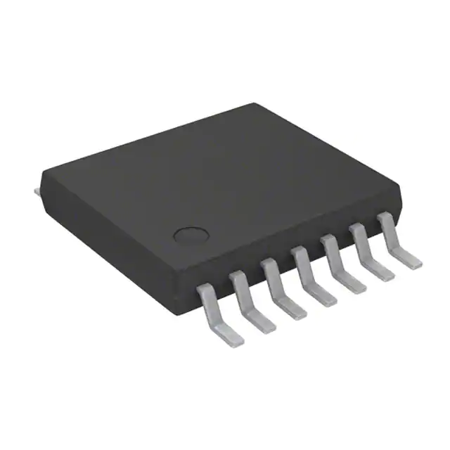


 工商网监
湘ICP备2023018690号
工商网监
湘ICP备2023018690号