MCP2140A
IrDA® Standard Protocol Stack Controller
With Fixed 9600 Baud Communication Rate
Features
Package Types
®
•
•
•
•
Low power, high-speed CMOS technology
Low voltage operation
Industrial temperature range
Low power consumption:
< 407 µA (maximum) @ 2.0V, 3.6864 MHz
2007-2011 Microchip Technology Inc.
1
2
3
4
5
6
7
8
9
RXPDREF
TXIR
PHACT
RESET
VSS
NC
TX
RX
RI
RXPD
CD
OSC1
OSC2/CLKI
VDD
RTS
CTS
DTR
DSR
18
17
16
15
14
13
12
11
10
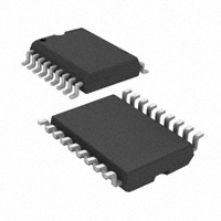
SSOP
RXPDREF
TXIR
PHACT
RESET
VSS
VSS
NC
TX
RX
RI
1
2
3
4
5
6
7
8
9
10
MCP2140A
CMOS Technology
PDIP, SOIC
MCP2140A
• Implements the IrDA Protocols, including:
- IrLAP
- IrLMP
- IAS
- Tiny TP
- IrCOMM (9-wire “cooked” service class)
• Provides IrDA standard physical signal layer
support including:
- Bidirectional communication
- CRC implementation
- Fixed Data communication rate of 9600 baud
• Includes UART-to-IrDA standard encoder/decoder
functionality:
Easily interfaces with industry standard
UARTs and infrared transceivers
• Easily communicates with 16-bit PIC
Microcontroller IrDA Standard Stack Library
• UART interface for connecting to Data
Communications Equipment (DCE) or Data
Terminal Equipment (DTE) systems
• Transmit/Receive formats (bit width) supported:
- 1.63 µs (Transmit & Receive)
- 3/16 bit time (Receive Only)
• Hardware UART Support:
- 9.6 kbaud baud rate
- 60 Byte Data Buffer Size (64 Byte Packet)
• Infrared Supported:
- 9.6 kbaud baud rate
- 64 Byte Packet Size (60 Data Bytes)
• Operates as Secondary Device
• Wide Operating Voltage: 2.0V to 5.5V
• Automatic Low Power mode:
< 23 µA (maximum) @ 2.0V, when
no IR activity present (PHACT = L)
• Footprint Compatibility with MCP2140
RXPD
CD
OSC1
OSC2/CLKI
VDD
VDD
RTS
CTS
DTR
DSR
20
19
18
17
16
15
14
13
12
11
Block Diagram
MCP2140A
TX
Encode and
Protocol Handler
TXIR
Logic
PHACT
RX
RTS
CTS
DSR
DTR
CD
RI
Baud
Rate
Generator
Protocol
Handler
and Decode
UART
Control
+
-
RXPD
RXPDREF
OSC1
OSC2/
CLKI
DS22050B-page 1
�MCP2140A
MCP2140A System Block Diagram
PIC®
Microcontroller
Optical
Transceiver
MCP2140A
TX
UART
SO
Encode
TXIR
TXD
Baud Rate
Generator
RX
UART Flow
Control (1)
I/O
I/O
I/O
I/O
I/O
I/O
MCP2140A
Status (1)
SI
I/O
RTS
CTS
DSR
DTR
CD
RI
PHACT
Decode
+
-
RXD
RXPD
RXPDREF
UART
Control
R1 (100 k)
0.1 µF
R2 (100 k)
Logic
Note 1: Not all microcontroller I/O pins are required to be connected to the MCP2140A.
DS22050B-page 2
2007-2011 Microchip Technology Inc.
�MCP2140A
1.0
DEVICE OVERVIEW
The MCP2140A is a cost-effective, low pin count (18pin), easy-to-use device for implementing IrDA standard wireless connectivity. The MCP2140A provides
support for the IrDA standard protocol “stack”, bit
encoding/decoding and low cost, discrete IR receiver
circuitry. The MCP2140A is footprint compatible with
the MCP2140. For migration assistance, please refer to
Section 2.14 “Migrating from the MCP2140 to the
MCP2140A”.
The serial and IR interface baud rates are fixed at
9600 baud. The serial interface and IR interface baud
rates are dependent on the device frequency, but IrDA
standard operation requires a device frequency of
3.6864 MHz.
The MCP2140A will specify the IR baud rate to the primary device during the Discover phase.
The MCP2140A can operate in Data Communication
Equipment (DCE) and Data Terminal Equipment (DTE)
applications, and resides between a UART and an
infrared optical transceiver.
The MCP2140A encodes an asynchronous serial data
stream, converting each data bit to the corresponding
infrared (IR) formatted pulse. IR pulses received are
decoded and then handled by the protocol handler
state machine. The protocol handler sends the appropriate data bytes to the host controller in UART
formatted serial data.
The MCP2140A supports “point-to-point” applications,
that is, one primary device and one secondary device.
The MCP2140A operates as a secondary device and
does not support “multi-point” applications.
Sending data using IR light requires some hardware
and the use of specialized communication protocols.
These protocol and hardware requirements are
described, in detail, by the IrDA standard specifications. The encoding/decoding functionality of the
MCP2140A is designed to be compatible with the physical layer component of the IrDA standard. This part of
the standard is often referred to as “IrPHY”.
Some of the devices that are compatible with the
MCP2140A include:
• PCs with IR ports
• PDAs
• 16-bit PIC Microcontroller IrDA Standard Stack
Library
1.1
Applications
The MCP2140A infrared communications controller,
supporting the IrDA standard, provides embedded system designers with the easiest way to implement IrDA
standard wireless connectivity. Figure 1-1 shows a typical application block diagram, while Table 1-2 shows
the pin definitions.
TABLE 1-1:
OVERVIEW OF FEATURES
Features
MCP2140A
Serial Communications
UART, IR
Baud Rate Selection
Fixed
Low Power Mode
Yes - Automatic
Resets (and Delays)
RESET, POR
(PWRT and OST)
Packages
18-pin DIP, SOIC,
20-pin SSOP
Infrared communication is a wireless, two-way data
connection using infrared light generated by low-cost
transceiver signaling technology. This provides reliable
communication between two devices.
Infrared technology offers:
• Universal standard for connecting portable
computing devices
• Easy, effortless implementation
• Economical alternative to other connectivity
solutions
• Reliable, high-speed connections
• Safe to use in any environment (can even be
used during air travel)
• No emissions testing needed (FCC, Part 15)
• Eliminates the hassle of cables
• Allows PCs and other electronic devices (such as
PDAs, cell phones, etc.) to communicate with
each other
• Enhances mobility by allowing users to easily
connect
The MCP2140A allows the easy addition of IrDA standard wireless connectivity to any embedded application that uses serial data. Figure 1-1 shows typical
implementation of the MCP2140A in an embedded
system.
The IrDA protocol for printer support is not included in
the IrCOMM 9-wire “cooked” service class.
More information about IrDA standards, specifications
and protocols can be found on the IrDA web site at
www.IrDA.org.
2007-2011 Microchip Technology Inc.
DS22050B-page 3
�MCP2140A
FIGURE 1-1:
SYSTEM BLOCK DIAGRAM
PIC®
Microcontroller
TX
UART
SO
UART Flow
Control (1)
Encode
TXIR
TXD
Baud Rate
Generator
RX
SI
MCP2140A
Status (1)
Optical
Transceiver
MCP2140A
I/O
I/O
I/O
I/O
I/O
I/O
I/O
RTS
CTS
DSR
DTR
CD
RI
PHACT
Decode
+
-
RXD
RXPD
RXPDREF
UART
Control
R1 (100 k)
0.1 µF
R2 (100 k)
Logic
Note 1: Not all microcontroller I/O pins are required to be connected to the MCP2140A.
DS22050B-page 4
2007-2011 Microchip Technology Inc.
�MCP2140A
TABLE 1-2:
Pin Name
MCP2140A PIN DESCRIPTION NORMAL OPERATION (DCE)
Pin Number
PDIP
SOIC SSOP
Pin
Type
Buffer
Type
Description
RXPDREF
1
1
1
I
A
IR Receive Photo Detect Diode Reference Voltage. This
voltage will typically be in the range of VDD/2.
TXIR
2
2
2
O
—
Asynchronous transmit to IrDA transceiver.
PHACT
3
3
3
OC
—
Protocol Handler Active. Indicates the state of the
MCP2140A Protocol Handler. This output is an open
collector, so an external pull-up resistor may be required.
1 = Protocol Handler is in the Discovery or NRM state
0 = Protocol Handler is in NDM state or the MCP2140A is in
Low Power mode
RESET
4
4
4
I
ST
VSS
5
5
5, 6
—
P
Ground reference for logic and I/O pins
Resets the Device
NC
6
6
7
I
—
No connect
TX
7
7
8
I
TTL
RX
8
8
9
O
—
RI
9
9
10
I
TTL
DSR
10
10
11
O
—
Data Set Ready. Indicates that the MCP2140A has established a valid IrDA link with a primary device(1). This signal is
locally emulated and not related to the DTR bit of the IrDA
primary device.
1 = An IR link has not been established
(No IR Link)
0 = An IR link has been established (IR Link)
DTR
11
11
12
I
TTL
Data Terminal Ready. Indicates that the Embedded device
connected to the MCP2140A is ready for IR data. The state
of this bit is communicated to the IrDA primary device via
the IrDA DSR bit carried by IrCOMM.
1 = Embedded device not ready
0 = Embedded device ready
CTS
12
12
13
O
—
Clear to Send. Indicates that the MCP2140A is ready to
receive data from the host controller. This signal is locally
emulated and not related to the CTS/RTS bit of the IrDA primary device.
1 = Host controller should not send data
0 = Host controller may send data
Asynchronous receive; from host controller UART
Asynchronous transmit; to host controller UART
Ring Indicator. The state of this bit is communicated to the
IrDA primary device.
1 = No Ring Indicate Present
0 = Ring Indicate Present
Legend:
TTL = TTL compatible input
A = Analog
CMOS = CMOS compatible input
I = Input
Note 1:
The state of the DSR output pin does not reflect the state of the DTR bit of the IrDA primary device.
2007-2011 Microchip Technology Inc.
ST = Schmitt Trigger input with CMOS levels
P = Power
OC = Open collector output
O = Output
DS22050B-page 5
�MCP2140A
TABLE 1-2:
Pin Name
MCP2140A PIN DESCRIPTION NORMAL OPERATION (DCE) (CONTINUED)
Pin Number
PDIP
SOIC SSOP
Pin
Type
Buffer
Type
Description
RTS
13
13
14
I
TTL
Request to Send. Indicates that a host controller is ready to
receive data from the MCP2140A. This signal is locally emulated and not related to the CTS/RTS bit of the IrDA primary
device.
1 = Host controller not ready to receive data
0 = Host controller ready to receive data
VDD
14
14
15, 16
—
P
Positive supply for logic and I/O pins.
—
Oscillator crystal output/external clock source input.
OSC2/CLKI
15
15
17
I/O
OSC1
16
16
18
I
CD
17
17
19
I
ST
Carrier Detect. The state of this bit is communicated to the
IrDA primary device via the IrDA CD bit.
1 = No carrier present
0 = Carrier present
RXPD
18
18
20
I
A
IR RX Photo Detect Diode input. This input signal is required
to be a pulse to indicate an IR bit. When the amplitude of the
signal crosses the amplitude threshold set by the RXPDREF
pin, the IR bit is detected.
CMOS Oscillator crystal input.
Legend:
TTL = TTL compatible input
A = Analog
CMOS = CMOS compatible input
I = Input
Note 1:
The state of the DSR output pin does not reflect the state of the DTR bit of the IrDA primary device.
DS22050B-page 6
ST = Schmitt Trigger input with CMOS levels
P = Power
OC = Open collector output
O = Output
2007-2011 Microchip Technology Inc.
�MCP2140A
2.0
DEVICE OPERATION
The MCP2140A serial interface and IR baud rates are
fixed at 9600 baud, given a 3.6864 MHz device clock.
2.1
POWER-ON AND BROWN-OUT
CONDITIONS
When any state machine is operated outside of its’
specified operating conditions, undesired operation
may occur. Application validation should be done to
determine when the system exits from either a PowerOn or a Brown-Out conditions if the MCP2140A
requires the use of an external voltage supervisory
circuit to ensure proper system operation.
2.2
XTAL
OSC2
To internal
logic
RF
RS
(Note)
C2
MCP2140A
See Table 2-1 and Table 2-2 for recommended
values of C1 and C2.
Note:
A series resistor may be required for
AT strip cut crystals.
TABLE 2-1:
CAPACITOR SELECTION FOR
CERAMIC RESONATORS
Freq
OSC1 (C1)
OSC2 (C2)
3.6864 MHz
10 - 22 pF
10 - 22 pF
Note:
Device Reset
Device Clocks
OSC1
C1
The MCP2140A is forced into the Reset state when the
RESET pin is in the low state. Once the RESET pin is
brought to a high state, the device Reset sequence
occurs. Once the sequence completes, functional
operation begins.
2.3
CRYSTAL OPERATION
(CERAMIC RESONATOR)
Ceramic
Resonator
Power-Up
Any time the device is powered up (Parameter D003),
the Power-Up Timer delay (Parameter 33) occurs, followed by an Oscillator Start-up Timer (OST) delay
(Parameter 32). Once these delays are complete, communication with the device may be initiated. This communication is from both the infrared transceiver’s side
and the controller’s UART interface.
2.1.1
FIGURE 2-1:
Higher capacitance increases the stability
of the oscillator, but also increases the
start-up time. These values are for design
guidance only. Since each resonator has
its own characteristics, the user should
consult the resonator manufacturer for
appropriate
values
of
external
components.
TABLE 2-2:
CAPACITOR SELECTION FOR
CRYSTAL OSCILLATOR
The MCP2140A requires a clock source to operate.
This clock source is used to establish the device timing,
including the device “Bit Clock”.
Freq
OSC1 (C1)
OSC2 (C2)
3.6864 MHz
15 - 30 pF
15 - 30 pF
2.3.1
Note:
CLOCK SOURCE
The clock source can be supplied by one of the
following:
• Crystal
• Resonator
• External clock
The frequency of this clock source must be
3.6864 MHz (electrical specification Parameter 1A) for
device communication at 9600 baud.
2.3.1.1
Higher capacitance increases the stability
of the oscillator but also increases the
start-up time. These values are for design
guidance only. RS may be required to
avoid overdriving crystals with low drive
level specification. Since each crystal has
its own characteristics, the user should
consult the crystal manufacturer for
appropriate
values
of
external
components.
Crystal Oscillator / Ceramic
Resonators
A crystal or ceramic resonator can be connected to the
OSC1 and OSC2 pins to establish oscillation (refer to
Figure 2-1). The MCP2140A oscillator design requires
the use of a parallel-cut crystal. Use of a series cut
crystals may give a frequency outside of the crystal
manufacturers specifications.
2007-2011 Microchip Technology Inc.
DS22050B-page 7
�MCP2140A
2.3.1.2
External Clock
For applications where a clock is already available
elsewhere, users may directly drive the MCP2140A
provided that this external clock source meets the AC/
DC timing requirements listed in Section 4.3 “Timing
Diagrams and Specifications”. Figure 2-2 shows
how an external clock circuit should be configured.
FIGURE 2-2:
EXTERNAL CLOCK
Clock From
external
system
2.3.2
CLKI
MCP2140A
BIT CLOCK
The device crystal is used to derive the communication
bit clock (BITCLK). There are 16 BITCLKs for each bit
time. The BITCLKs are used for the generation of the
start bit and the eight data bits. The stop bit uses the
BITCLK when the data is transmitted (not for
reception).
This clock is a fixed-frequency and has minimal variation in frequency (specified by the crystal
manufacturer).
DS22050B-page 8
2007-2011 Microchip Technology Inc.
�MCP2140A
2.4
Host UART Interface
The host UART interface communicates with the host
controller. This interface has eight signals associated
with it: TX, RX, RTS, CTS, DSR, DTR, CD and RI. Several of these signals are locally generated (not passed
over the IR interface). The host UART is a full-duplex
interface, meaning that the system can transmit and
receive simultaneously.
Note 1: The MCP2140A generates several nondata signals locally.
2: The MCP2140A emulates a 3-wire serial
connection (TXD, RXD and GND). The
transceiver’s transmit data (TXD), receive
data (RXD) signals, and the state of the
CD. RI and DTR input pins are carried
back and forth to the primary device.
3: The RTS and CTS signals are local
emulations.
2.4.1
BAUD RATE
The baud rate for the MCP2140A serial port (the TX
and RX pins) is fixed at 9600 baud when the device
frequency is 3.6864 MHz.
2.4.2
TRANSMITTING
When the host controller sends serial data to the
MCP2140A, the host controller’s baud rate is required
to match the baud rate of the MCP2140A’s serial port.
2.4.3
RECEIVING
When the host controller receives serial data from the
MCP2140A, the host controller’s baud rate is required
to match the baud rate of the MCP2140A’s serial port.
2.4.4
HARDWARE HANDSHAKING
There are three host UART signals used to control the
handshaking operation between the host controller and
the MCP2140A.
The following signals are host UART signals:
• DSR
• RTS
• CTS
2.4.4.1
2.4.4.2
RTS
The RTS signal indicates to the MCP2140A that the
host controller is ready to receive serial data.
Once an IR packet with “data” has been received by the
MCP2140A, the RTS signal will need to be low for the
received data to be transferred to the host controller. If
the RTS signal remains high, an IR link timeout will
occur and the MCP2140A will disconnect from the primary device.
2.4.4.3
CTS
The CTS signal indicates that the MCP2140A UART
receive buffer is full. The MCP2140A generates the
CTS signal locally.
The MCP2140A UART receive buffer is 60 bytes and
the CTS signal will be driven high once 59 bytes have
been received.
After the MCP2140A UART has received a byte, there
is a latency before the CTS signal is driven high, if the
UART receive buffer has 59 bytes. The MCP2140A
then supports the reception of another byte (the 60th
byte). This allows a byte was being received when CTS
was driven high not to be lost. The MCP2140A UART
receive buffer supports 60 bytes, regardless if the last
byte started transmission before or after the CTS signal
was driven high.
Note:
When the CTS output signal goes high, the
UART FIFO will store up to 1 additional
byte, for a maximum of 60 bytes.
The MCP2140A has a buffer for incoming data from the
IR host. This buffer supports the 60-byte data payload
plus the memory overhead of the packet. Another
60 byte buffer is provided to buffer data from the UART
serial port. The MCP2140A can handle IR data and
host UART serial port data simultaneously. A hardware
handshaking pin (CTS) is provided to inhibit the host
controller from sending serial data when the host UART
buffer is not available. Figure 2-3 shows CTS states
while Figure 2-4 shows an example of the CTS signal
when the host controller streams 250 bytes to the
MCP2140A. Figure 2-5 shows a flow chart for host
UART flow control using the CTS signal.
DSR
The DSR signal indicates that the MCP2140A has
established a link between the MCP2140A and the primary device. Please refer to Appendix B: “How
Devices Connect” for more information.
2007-2011 Microchip Technology Inc.
DS22050B-page 9
�MCP2140A
FIGURE 2-3:
HOST UART CTS SIGNAL AND THE RECEIVE BUFFER
CTS
Receive Buffer Empty
MCP2140A Can
Receive Data
FIGURE 2-4:
Receive Buffer
Full (60 Bytes)
IR Data Packet Transmitted
Receive Buffer Empty
MCP2140A Can Receive Data
Receive Buffer Has 59 Bytes,
CTS Pin Driven High
IR Data Packet Starts Transmission
CTS WAVEFORM FROM HOST CONTROLLER STREAMING OF 250 BYTES TO
THE MCP2140A
CTS
DS22050B-page 10
2007-2011 Microchip Technology Inc.
�MCP2140A
FIGURE 2-5:
HOST UART CTS FLOW CONTROL FLOWCHART
IR Flow Start
Host
Transmit
Buffer
Avail?
No
Yes
Yes
More
Bytes To
Transmit?
DTR Low?
No
No
Yes
Return
CTS Low?
No
Yes
Transmit Byte
2007-2011 Microchip Technology Inc.
DS22050B-page 11
�MCP2140A
2.5
Encoder/Decoder
The encoder converts the UART format data into the
IrDA standard format data and the decoder converts
IrDA standard format data into UART format data.
2.5.1
ENCODER (MODULATION)
The data that the MCP2140A UART received (on the
TX pin) that needs to be transmitted (on the TXIR pin)
is modulated. This modulated signal drives the IR
transceiver module. Figure 2-6 shows the encoding of
the modulated signal.
Note:
Each bit time is comprised of 16-bit clocks. If the value
to be transmitted (as determined by the TX pin) is a
logic-low, the TXIR pin will output a low level for 7-bit
clock cycles, a logic high level for 3-bit clock cycles or
a minimum of 1.6 µs (see Parameter IR121). The
remaining 6-bit clock cycles will be low. If the value to
transmit is a logic-high, the TXIR pin will output a low
level for the entire 16-bit clock cycles.
The signal on the TXIR pin does not actually line up in time with the bit value that
was transmitted on the TX pin, as shown
in Figure 2-6. The TX bit value is shown to
represent the value to be transmitted on
the TXIR pin.
FIGURE 2-6:
ENCODING
Start Bit
16 CLK
Data bit 0
Data bit 1
Data bit 2
Data bit ...
0
0
1
BITCLK
TX Bit
Value
7 CLK
TXIR
12 Tosc
0
DS22050B-page 12
1
0
2007-2011 Microchip Technology Inc.
�MCP2140A
2.5.2
2.6
DECODER (DEMODULATION)
The modulated signal (data) from the IR transceiver
module (on the RXIR pin) is demodulated to form the
received data (on the RX pin). Once demodulation of
the data byte occurs, the data that is received is transmitted by the MCP2140A UART (on the RX pin).
Figure 2-7 shows the decoding of the modulated
signal.
Note:
IR Port Baud Rate
The baud rate for the MCP2140A IR port (the TXIR and
RXIR pins) is fixed at the default rate of 9600 baud. The
primary device will be informed of this parameter during
NDM. The host UART baud rate and the IR port baud
rate are the same.
The signal on the RX pin does not actually
line up in time with the bit value that was
received on the RXIR pin, as shown in
Figure 2-7. The RXIR bit value is shown to
represent the value to be transmitted on
the RX pin.
Each bit time is comprised of 16-bit clocks. If the value
to be received is a logic-low, the RXIR pin will be a low
level for the first 3-bit clock cycles, or a minimum of
1.6 µs. The remaining 13-bit clock cycles (or difference
up to the 16-bit clock time) will be high. If the value to
be received is a logic-high, the RXIR pin will be a high
level for the entire 16-bit clock cycles. The level on the
RX pin will be in the appropriate state for the entire 16
clock cycles.
FIGURE 2-7:
DECODING
Start Bit
Data bit 0
Data bit 1
Data bit 2
Data bit ...
16 CLK
16 CLK
16 CLK
0
0
16 CLK
BITCLK
(CLK)
RXIR Bit Value
RXPD
RXPDREF
13 CLK
1.6 µs (up to 3 CLK)
16 CLK
16 CLK
16 CLK
RX
0
2007-2011 Microchip Technology Inc.
1
1
0
DS22050B-page 13
�MCP2140A
2.7
IrDA Data Protocols Supported by
MCP2140A
The MCP2140A supports these required IrDA standard
protocols:
• Physical Signaling Layer (PHY)
• Link Access Protocol (IrLAP)
• Link Management Protocol/Information Access
Service (IrLMP/IAS)
The MCP2140A also supports some of the optional
protocols for IrDA standard data. The optional
protocols implemented by the MCP2140A are:
• Tiny TP
• IrCOMM
2.7.1
IrCOMM
IrCOMM provides the method to support serial and parallel port emulation. This is useful for legacy COM
applications, such as printers and modem devices.
The IrCOMM standard is a syntax that allows the primary device to consider the secondary device a serial
device. IrCOMM allows for emulation of serial or parallel (printer) connections of various capabilities. The
MCP2140A supports the 9-wire “cooked” service class
of IrCOMM. Other service classes supported by
IrCOMM are shown in Figure 2-9.
The IrDA protocol for printer support is not included in
the IrCOMM 9-wire “cooked” service class.
Figure 2-8 shows the IrDA data protocol stack and
those components implemented by the MCP2140A.
FIGURE 2-8:
IrDA DATA - PROTOCOL
STACKS
IrObex IrLan IrCOMM(1)
IrTran-P
LM-IAS
IrMC
Tiny Transport Protocol (Tiny TP)
IR Link Management - Mux (IrLMP)
IR Link Access Protocol (IrLAP)
Asynchronous
Synchronous Synchronous
4 PPM
Serial IR
Serial IR (2, 3)
(4
Mb/s)
(1.152
Mb/s)
(9600 -115200 b/s)
Supported by
the MCP2140A
Optional IrDA data
protocols not
supported by
the MCP2140A
Note 1: The MCP2140A implements the 9-wire
“cooked” service class serial replicator.
2: The MCP2140A is fixed at 9600 baud
3: An optical transceiver is required.
FIGURE 2-9:
IRCOMM SERVICE CLASSES
IrCOMM Services
Uncooked Services
Cooked Services
Parallel
Serial
Parallel
Serial
IrLPT
3-wire Raw
Centronics
3-wire Cooked
IEEE 1284
9-wire Cooked
Supported by MCP2140A
DS22050B-page 14
2007-2011 Microchip Technology Inc.
�MCP2140A
2.8
Minimizing Power
During IR communication between a primary device
and the MCP2140A, the MCP2140A is in an operational mode. In this mode, the MCP2140A consumes
the operational current (Parameter D010A).
For many applications, the time that IR communication
is occurring is a small percentage of the applications
operational time. The ability for the IR controller to be
in a low power mode during this time will save on the
applications power consumption. The MCP2140A will
automatically enter a low power mode once IR activity
has stopped and will return to operational mode once
IR activity is detected on the RXPD and RXPDREF
pins. The PHACT pin indicates if the protocol handler is
active or inactive (Low Power mode).
Another way to minimize system power is to use an I/O
pin of the host controller to enable power to the IR
circuity
2.8.1
AUTOMATIC LOW POWER MODE
The Automatic Low Power mode allows the system to
achieve the lowest possible operating current.
When the IR link has been “closed”, the protocol
handler state machine returns to the Normal
Disconnect Mode (NDM). During NDM, if no IR activity
occurs for about 10 seconds, the device is disabled and
enters into Low Power mode. In this mode, the device
oscillator is shut down and the PHACT pin will be low
(Parameter D010B).
Table 2-3 shows the MCP2140A current. These are
specified in Parameter D010A and Parameter D010B.
TABLE 2-3:
DEVICE MAXIMUM
OPERATING CURRENT
Mode
Current
PHACT = H
407 µA
IR communication is occurring (or waiting for timeout).
PHACT = L
23 µA
No IR communications.
Note:
2.8.2
Comment
Additional system current is from the
receiver/transmitter and the RXPDREF
voltage reference circuitry.
RETURNING TO DEVICE
OPERATION
The device will exit the Low Power mode when the
RXPD pin voltage crosses the REPDREF pin reference
voltage.
A device Reset will also cause the MCP2140A to exit
Low Power mode. After device initialization, if no IR
activity occurs for about 10 seconds, the device returns
to the Low Power mode.
Note:
2.9
For proper operation, the device oscillator
must be within oscillator specification in
the time frame specified in Parameter
IR140.
PHACT Signal
The PHACT signal indicates that the MCP2140 protocol handler is active. This output pin is an open collector; so, when interfacing to the host controller, a pull-up
resistor is required.
2007-2011 Microchip Technology Inc.
DS22050B-page 15
�MCP2140A
2.10
Buffers and Throughput
Figure 2-11 shows an example communications
sequence between a primary device and a secondary
device (MCP2140A). In this example, after the “Primary
Device Sends Open Link Frame”, the time for the secondary device’s response is fixed by the operation of
the MCP2140A. After the “Primary Device Decodes
Secondary Device Response” the “Primary Device
Responds to Secondary Device”. Throughput may be
improved if the application program can be written so
that the primary device response is fast as possible.
Also, when the “Secondary Device Sends Data”, the
frame should have the maximum number of data bytes.
The IR data rate of the MCP2140A is fixed at
9.6 kbaud. The actual throughput will be less due to
several factors. Many significant factors are under the
control of the developer. One factor beyond the control
of the designer is the overhead associated with the
IrDA standard.
Depending on the application, throughput may be an
issue in one or both directions.
2.10.1
THROUGHPUT
Throughput is dependant on the direction that the data
is streaming and the characteristics of the primary
device and secondary device. Streaming throughput
from the secondary device may be different with different primary devices. Also streaming throughput from
the secondary device may be different than streaming
throughput to the secondary device, with the same primary device. Throughput examples are shown in
Table 2-4. These examples are based on actual
observed data communications.
Note:
Figure 2-12 shows the screen-capture of a host controller (and MCP2140A) streaming (transmitting) 250
bytes to a primary device (PIC24 + IrDA Standard Stack
Library).
Figure 2-13 shows the screen-capture of a MCP2140A
(and host controller) receiving 250 streamed bytes from
a primary device (PIC24 + IrDA Standard Stack
Library).
Figure 2-14 shows a second screen-capture of a host
controller (and MCP2140A) streaming (transmitting)
250 bytes to a primary device (PDA HP IPAQ H2495B).
IrDA throughput is based on many factors
associated with characteristics of the primary and secondary devices. These characteristics may cause your throughput to
be more or less than is shown in Table 2-4.
Figure 2-15 shows a second screen capture of a host
controller (and MCP2140A) streaming (transmitting)
250 bytes to a primary device (PDA HP IPAQ H2495B).
THROUGHPUT EXAMPLES - 250 BYTES (3)
TABLE 2-4:
Primary Device
PC (6)
Secondary
Device
Data
Streaming
Direction
250 Byte
Transmit Time
(ms) (1)
Effective
Comment
Baud Rate (2)
MCP2140A (5)
S -> P
354
7062
MCP2140
S -> P
650 (7)
3692
Figure 2-14
Note 7
PIC IrDA Standard Stack (4) MCP2140A (5)
S -> P
337
7418
Figure 2-12
PIC IrDA Standard Stack (4) MCP2140A (5)
P -> S
549
4553
Figure 2-13
(5)
S -> P
332
7530
Figure 2-15
PDA (HP iPAQ hx2495b)
Note 1:
2:
3:
4:
5:
6:
7:
MCP2140A
Measured from Figure. (see comment)
Interpolated from Figure. (see comment)
10 bits transferred for each byte.
Using the PIC24 Explorer 16 Development Board with IR Transceiver Board
Using the MCP215X/40 Data Logger Demo Board and Board Firmware V1.4
IBM 600X Thinkpad (notebook computer) running Windows XP Professional (SP1)
MCP2140 Data Sheet, DS21790, Table 2-4, MCP2140 transmitted 240 bytes in this transmit time.
FIGURE 2-10:
CTS
HOST UART RECEIVE BUFFER AND CTS WAVEFORM
Receive Buffer
Full (60 Bytes)
IR Data Packet Transmitted
Receive Buffer Empty
Receive Buffer Empty
MCP2140A Can Receive Data
Receive Buffer Has 59 Bytes,
MCP2140A Can Receive Data CTS Pin Driven High
IR Data Packet Starts Transmission
DS22050B-page 16
2007-2011 Microchip Technology Inc.
�MCP2140A
FIGURE 2-11:
EXAMPLE IR COMMUNICATION SEQUENCE
Primary Device Secondary Device Secondary Device Primary Device
Primary Device
Sends Open
Decodes Open
Responds to
Decodes Secondary Responds to
Link Frame
Link Frame
Open Link Frame Device Response
Secondary Device
Secondary Device
Primary Device
Primary Device
Secondary Device
Decodes Primary
Decodes Received Responds to
Sends Data
Devices Response
Data
Secondary Device
Secondary Device
Primary Device
Primary Device
Secondary Device
Decodes Primary
Decodes Received Responds to
Sends Data
Devices Response
Data
Secondary Device
FIGURE 2-12:
HOST CONTROLLER TRANSMISSION (S P) OF A 250 BYTE PACKET
(TO PIC IrDA STANDARD STACK)
2007-2011 Microchip Technology Inc.
DS22050B-page 17
�MCP2140A
FIGURE 2-13:
DS22050B-page 18
HOST CONTROLLER RECEPTION (P S) OF A 250 BYTE PACKET
(FROM PIC IRDA STANDARD STACK)
2007-2011 Microchip Technology Inc.
�MCP2140A
FIGURE 2-14:
HOST CONTROLLER TRANSMISSION (S P) OF A 250 BYTE PACKET
(TO PC WITH IRDA PORT)
2007-2011 Microchip Technology Inc.
DS22050B-page 19
�MCP2140A
FIGURE 2-15:
DS22050B-page 20
HOST CONTROLLER TRANSMISSION (S P) OF A 250 BYTE PACKET
(TO PDA HP IPAQ H2495B)
2007-2011 Microchip Technology Inc.
�MCP2140A
2.10.2
IMPROVING THROUGHPUT
2.10.2.3
Actual maximum throughput is dependent on several
factors, including:
•
•
•
•
Characteristics of the primary device
Characteristics of the MCP2140A
IrDA standard protocol overhead
Direction of Data Transmitted
2.10.2.1
Characteristics of the Primary
Device and the MCP2140A
IrDA standard protocol overhead limits the maximum
throughput to much less then the 9600 baud bit rate.
IrDA Standard Protocol Overhead
The IrDA standard specifies how the data is passed
between the primary device and secondary device. In
IrCOMM, an additional 8 bytes are used by the protocol
for each packet transfer. In the IrCOMM 9-wire
“cooked” service class, 4 bytes of the 64 byte payload
are overhead bytes. That leaves a maximum of
60 bytes that can be transferred per “frame”.
The most significant factor in data throughput is how
well the data frames are filled. If only 1 byte is sent at a
time, the throughput overhead of the IrCOMM protocol
is 89% (see Table 2-5). The best way to maximize
throughput is to align the amounts of data with the
receive buffer (IR and host UART) packet size of the
MCP2140A.
TABLE 2-5:
IRCOMM OVERHEAD %
Data
IrCOMM IrCOMM
Packet
MCP2140A
Overhead Overhead Comment
Size
(Bytes)
% (1)
(Bytes)
IR Receive
Host UART
Receive
60
8
12 %
1
8
89 %
60
8
12 %
1
8
89 %
Due to the different characteristics of the primary
device and the secondary device, the data throughput
between two devices may be substantially different
depending on the direction the data is being transferred. This is shown in Table 2-4.
MCP2140A to Primary Device
While the characteristics of the MCP2140A are fixed,
the characteristics of the primary device may be made
better, or worse, depending on the implementation of
the primary device’s application program.
2.10.2.2
Direction of Data Transmitted
Note 2
Note 3,
Note 4
One of the factors to improve throughput is to ensure
the host controller keeps the MCP2140A UART receive
buffer full (60 bytes) to maximize the data bytes sent
per IR frame. Figure 2-10 shows the CTS waveform,
what the state of the buffers can be and the operation
of the host UART and IR interfaces.
The second factor is to minimize the turnaround
response time from the primary device, if possible.
Primary Device to MCP2140A
In this case, ensure that the host controller can receive
data as fast as possible from the MCP2140A without
requiring to force the RTS high and delay the data from
being received by the host controller.
2.10.2.4
From the Primary Device
The MCP2140A uses a fixed IR Receiver data block
size of 64 bytes.
The minimum size frame the primary device can
respond with is 6 bytes.
2.10.2.5
From the MCP2140A
The MCP2140A uses a fixed host UART receiver data
block size of 60 bytes.
2.11
Turnaround Latency
An IR link can be compared to a one-wire data connection. The IR transceiver can transmit or receive, but not
both at the same time. A delay of one bit time is recommended between the time a byte is received and
another byte is transmitted.
2.12
Device ID
The MCP2140A has a fixed Device ID. This Device ID
is “MCP2140A XX”, with the xx indicating the silicon
revision of the device.
Note 1: Overhead % =
Overhead/(Overhead + Data).
2: The maximum number of data bytes in the
IR receive frame.
3: The maximum number of bytes of the host
UART receive buffer.
4: The CTS signal is driven high after the 59
byte.
2007-2011 Microchip Technology Inc.
DS22050B-page 21
�MCP2140A
2.13
Optical Interface
The MCP2140A requires an infrared transceiver for the
optical interface. This transceiver can be a single-chip
solution (integrated) or be implemented with discrete
devices.
The MCP2140A was designed to interface to a integrated optical transceiver, although it can interface to a
discrete solution as long as the MCP2140A
specifications are meet.
Note:
Figure 2-18 shows a simple “Blue Wire” modification
that can be done.
Table 2-8 shows a list of common manufacturers of
integrated optical transceivers.
FIGURE 2-16:
MCP2140 WAVE SHAPING
CIRCUIT FOR
INTEGRATED OPTICAL
TRANSCEIVER
+5V
Please refer to Appendix F: “Device
Errata” for additional information on the
optical transceiver.
The MCP2140 required a wave shaping circuit to interface to typical integrated optical transceivers. An example circuit is shown in the user guides of the MCP2140
demo and evaluation boards. This circuit is shown in
Figure 2-16. This circuit inverts the optical transceivers
RXD signal.
The MCP2140A requires that the RXD signal is not
inverted. Figure 2-17 shows how the Microchip example wave shaping circuit can be modified with simple
component replacement to support the MCP2140A.
Figure 2-19 shows the RXD signal characteristics
before and after the modified wave shaping circuit
(Figure 2-17).
Table 2-6 shows the schematic symbols for the example MCP2140 wave shaping circuit, and the component
changes required to make the PCB layout compatible
with the MCP2140A. The layout is not required to be
changed since the BAT54 is a Schottky diode in a
SOT-23-3 package with the desired pin connections,
the capacitor footprint can easily be replaced by a
resistor (0), and the R16 resistor can be removed
since it is not involved with the circuit.
R16
100
R13
optional
2
RXD
1
C19
R11
47 pF optional
+5V
Q1
MMUN2111LT1
3
R20
4.7 k
R14
10 k
R15
10 k
RXPD
(MCP2140
Pin 18)
RXPDREF
(MCP2140 Pin 1)
FIGURE 2-17:
MCP2140A
MODIFICATIONS OF
MCP2140 WAVE SHAPING
CIRCUIT
+5V
TABLE 2-6:
EXAMPLE MCP2140 WAVE
SHAPING CIRCUIT TO
MCP2140A COMPONENT
CHANGES
R16 (Open)
R13
optional
Component
Symbol
MCP2140 Device
(value)
MCP2140A
Device (value)
C19
Capacitor (47pF)
Resistor (0 ) (1)
R11
—
—
R13
—
—
R16
Resistor
(100)
—
R20
Resistor
(4.7 k)
Resistor
(4.7 K) (1)
PNP Transistor
(MMUN2111LT1)
Schottky Diode
(BAT54) (1)
Q1
(SOT-23-3)
RXD
1
C19
0
R11
optional
+5V
Q1
BAT54
3
Schottky
Diode R20
4.7 k
RXPD
(MCP2140A
Pin 18)
R14
10 k
R15
10 k
RXPDREF
(MCP2140A Pin 1)
Note 1: This device is changed from MCP2140
wave shaping circuit implementation.
DS22050B-page 22
2007-2011 Microchip Technology Inc.
�MCP2140A
FIGURE 2-18:
MCP2140A “BLUE WIRE” MODIFICATIONS OF MCP2140 WAVE SHAPING
CIRCUIT
+5V
R16 (Open)
R13
optional
Q1
RXD
C19
R11
optional
“Blue Wire”
+5V
R20
4.7 k
RXPD
(MCP2140A
Pin 18)
R14
10 k
R15
10 k
FIGURE 2-19:
RXPDREF
(MCP2140A Pin 1)
MCP2140A MODIFICATIONS OF MCP2140 WAVE SHAPING CIRCUIT
2007-2011 Microchip Technology Inc.
DS22050B-page 23
�MCP2140A
2.14
Migrating from the MCP2140 to the
MCP2140A
This section shows you in the major differences
between the MCP2140 and the MCP2140A. Your application may have other sensitivities and a complete
system validation should be done.
Table 2-7 shows the differences and enhancements of
the MCP2140A in comparison to the MCP2140.
TABLE 2-7:
DIFFERENCE BETWEEN
MCP2140 AND MCP2140A
Feature
MCP2140
Voltage Range
3.0V - 5.5V 2.0V - 5.5V
Frequency of Operation
(MHz)
UART operation
7.3728
MCP2140A
3.6864
Half Duplex Full Duplex
29
UART Transmit Buffer
Size (bytes) (max.)
29
IR Receiver Frame
Payload Size (bytes)
(max.)
64 (3)
IR Transmit Frame
Payload Size (bytes)
(max.)
64
(3)
Max IDD (uA) PHACT = H
at min. VDD. PHACT = L
2200
407
60
23
Required
Not
Required
60
64 (3)
64
The PIC IrDA Standard Stack
Library and the MCP2140A
The MCP2140A is compatible with the PIC IrDA Standard Stack Library routines for 16-bit PIC microcontrollers. The application must use the Client Library
routines for the IrCOMM 9-wire cooked protocol (for primary device operation).
2.16
References
The IrDA standards organization information can be
found at:
http://www.irda.org
Some common manufacturers of optical transceivers
are shown in Table 2-8.
TABLE 2-8:
(2)
UART Receiver Buffer
Size (bytes) (max.)
Integrated Optical
Transceivers RXD
Wave Shaping Circuit
60
2.15
(3)
Company
COMMON OPTICAL
TRANSCEIVER
MANUFACTURERS
Company Web Site Address
Sharp®
www.sharpsma.com
Infineon®
www.infineon.com
Agilent®
www.agilent.com
Vishay®
www.vishay.com
Rohm®
www.rohm.com
(1)
Optical Transceiver RXPD High to Low High to Low
bit signal polarity
or
only
Low to High
Note 1: The external wave shaping circuit is not
required. For applications replacing the
MCP2140, components of the circuit can
be replaced to effectively remove the
waveshaping circuit. See Section 2.13
“Optical Interface”.
2: The MCP2140A will drive the CTS signal
active after the UART receive buffer has
59 bytes. The Receive buffer supports the
reception of a 60th byte for systems that
have 0 delay between UART data bytes.
3: Includes 4 bytes overhead for 9-wire
“cooked” protocol. This means that there
are a maximum of 60 data bytes per
frame.
DS22050B-page 24
2007-2011 Microchip Technology Inc.
�MCP2140A
3.0
DEVELOPMENT TOOLS
The MCP2140A currently has three Demo/Development boards that can be used to demonstrate or
evaluate the MCP2140A. These boards are:
• MCP215x/40 Data Logger Demo Board
• MCP215x/40 Developers Daughter Board
• MCP2140 Wireless Temp Sensor Demo Board
These boards have not been tested with the
MCP2140A. However, the supplied MCP2140 device
can easily be replaced with the MCP2140A. The waveshaping circuit for the MCP2140 will need to be modified. See Section 2.13 “Optical Interface” for
additional information on modifying the MCP2140
wave shaping circuit.
Please check with the Microchip Technology Inc. web
site (www.microchip.com) for additional boards and
technical information.
3.1
MCP215X/40 Data Logger Demo
Board
Part Number: MCP215XDM
Devices Supported: MCP2150, MCP2155,
MCP2140, and MCP2140A
The MCP215X IrDA Data Logger Demo Board demonstrates the MCP2150 (or MCP2155) IrDA Standard
Protocol Stack Controller device in a real world application. The system designer can use this design as an
example of how to integrate an IrDA standard port in
their embedded system.
Note:
Use of the MCP2140A will require that the
MCP2140 wave shaping circuit be
modified. See Section 2.13.
FIGURE 3-1:
MCP215X/40 DATA
LOGGER DEMO BOARD
Features:
• Demonstrates the MCP2150 IrDA Protocol
Controller in a data logging application
• Communicates directly to a Laptop computer,
Palm or Pocket PC PDA
• Primary device application programs are provided
to demonstrate operation (for PC, Palm OS,
Pocket PC)
• F/W routines transmit data to a primary device
(i.e., Laptop, PDA)
• LCD display indicates system state
• Reprogrammable PIC16F877 with ICSP™
(In-Circuit Serial Programming™) interface and
ICD header
• Interface Header allows board to be interfaced to
a prototype system application
• Header allows other optical transceiver circuits to
be interfaced to the MCP215X device
• Operates on 9V DC input or a 9V battery
2007-2011 Microchip Technology Inc.
DS22050B-page 25
�MCP2140A
3.2
MCP215X/40 Developer's
Daughter Board
Part Number: MCP215X/40EV-DB
Devices Supported: MCP2150, MCP2155,
MCP2140, and MCP2140A
The MCP215X/40 Developer’s Daughter Board is used
to evaluate and demonstrate the MCP2140 IrDA Standard Protocol Stack Controller with encoder/decoder
devices.
Headers allow the MCP215X/40 Developer’s Daughter
Board to be easily jumpered into systems for
development purposes.
The MCP215X/40 Developer’s Daughter Board is
designed to interface to several of the new low-cost
Microchip demo boards. These include the PIC18
Explorer Demo Board, the PICDEM™ Full Speed USB
Demo Board, the PICDEM 2 Plus Demo Board, and the
PICDEM LCD 2 Demo board.
Features:
• 18-pin socket for installation of MCP2150,
MCP2155, or MCP2140 device
• Three optical transceiver circuits (1 installed)
• MCP2140 optical transceiver waveshaping circuit
• Headers to interface to low-cost PICDEM Demo
Boards, including:
- PIC18 Explorer Demo Board
- PICDEM LCD 2 Demo Board
- PICDEM Full Speed USB Demo Board
- PICDEM 2 Plus Demo Board
• Headers to easily connect to the user’s
embedded system
• Jumpers to select circuit connections between
MCP2150, MCP2155, and MCP2140
• Jumpers to select routing of MCP215X/40 signals
to the PICDEM demo board headers
• Jumpers to configure the operating mode of the
board
When the MCP215X/40 Developer’s Daughter Board is
used in conjunction with the PIC18 Explorer Demo
Board, the MCP215X or MCP2140 can be connected
to either of the UARTs on the PIC18F8772 two or the
RX and TX signals can be “crossed” so the MCP215X
or MCP2140 device can communicate directly out the
PIC18 Explorer Demo Board's UART (DB-9).
FIGURE 3-2:
DS22050B-page 26
MCP215X/40
DEVELOPER'S
DAUGHTER BOARD
2007-2011 Microchip Technology Inc.
�MCP2140A
3.3
MCP2140 IrDA Wireless Temp
Sensor Demo Board
Part Number: MCP2140DM-TMPSNS
Devices Supported: MCP2140 and
MCP2140A
The MCP2140 IrDA Wireless Temp Sensor Demo
Board demonstrates the MCP2140 device in a real
world application. The system designer can use this
design as an example of how to integrate an IrDA standard port in their system.
Note:
Use of the MCP2140A will require that the
MCP2140 wave shaping circuit be
modified. See Section 2.13.
FIGURE 3-3:
Features:
• Demonstrates the MCP2140 IrDA Protocol
Controller in a data logging application
• Communicates directly to a laptop computer,
Palm or Pocket PC PDA
• Primary device application programs are provided
to demonstrate operation (for PC, Palm OS,
Pocket PC)
• Demonstrates the MCP2140 IrDA Protocol
Controller in a data logging application
• F/W routines transmit TC1047A temperature and
other data to a primary device (i.e., laptop, PDA)
• Reprogrammable PIC18F1320 with ICSP™
(In-Circuit Serial Programming™) interface and
ICD header
• Operates on 3 AAA alkaline batteries
MCP2140 IRDA WIRELESS
TEMP SENSOR DEMO
BOARD
2007-2011 Microchip Technology Inc.
DS22050B-page 27
�MCP2140A
NOTES:
DS22050B-page 28
2007-2011 Microchip Technology Inc.
�MCP2140A
4.0
ELECTRICAL CHARACTERISTICS
Absolute Maximum Ratings†
Ambient Temperature under bias ........................................................................................................... –40°C to +125°C
Storage Temperature ............................................................................................................................. –65°C to +150°C
Voltage on VDD with respect to VSS ........................................................................................................... -0.3V to +6.5V
Voltage on RESET with respect to VSS ...................................................................................................... -0.3V to +14V
Voltage on all other pins with respect to VSS ................................................................................. –0.3V to (VDD + 0.3V)
Total Power Dissipation (1) ...................................................................................................................................800 mW
Max. Current out of VSS pin ..................................................................................................................................300 mA
Max. Current into VDD pin .....................................................................................................................................250 mA
Input Clamp Current, IIK (VI < 0 or VI > VDD) 20 mA
Output Clamp Current, IOK (V0 < 0 or V0 > VDD) 20 mA
Max. Output Current sunk by any Output pin..........................................................................................................25 mA
Max. Output Current sourced by any Output pin.....................................................................................................25 mA
Note 1: Power Dissipation is calculated as follows: PDIS = VDD x {IDD - IOH} + {(VDD-VOH) x IOH} + (VOL x IOL)
†NOTICE:
Stresses above those listed under “Maximum ratings” may cause permanent damage to the device. This is
a stress rating only and functional operation of the device at those or any other conditions above those indicated in
the operational listings of this specification is not implied. Exposure to maximum rating conditions for extended periods
may affect device reliability.
Note:
Voltage spikes below VSS at the RESET pin, inducing currents greater than 80 mA, may cause latch-up.
Thus, a series resistor of 50 - 100 should be used when applying a “low” level to the RESET pin rather
than pulling this pin directly to VSS.
2007-2011 Microchip Technology Inc.
DS22050B-page 29
�MCP2140A
VOLTAGE-FREQUENCY GRAPH, -40C TA +85C
FIGURE 4-1:
6.0
5.5
5.0
4.5
VDD 4.0
(Volts)
3.5
3.0
2.5
2.0
0
4
3.6864
8
10
12
16
20
Frequency (MHz)
DS22050B-page 30
2007-2011 Microchip Technology Inc.
�MCP2140A
4.1
DC Characteristics
Electrical Characteristics:
Standard Operating Conditions (unless otherwise specified)
Operating Temperature: -40C TA +85C (industrial)
DC Specifications
Param.
No.
Sym
Characteristic
Min
Typ(1)
Max
Units
Conditions
D001
VDD
Supply Voltage
2.0
—
5.5
V
See Figure 4-1
D002
VDR
RAM Data Retention
Voltage (2)
2.0
—
—
V
Device Oscillator/Clock stopped
D003
VPOR
VDD Start Voltage to
ensure Power-on Reset
—
VSS
—
V
D004
SVDD
VDD Rise Rate to
ensure Power-on Reset
0.05
—
—
V/ms
D010A
IDD
—
—
23
µA
VDD = 2.0V, PHACT = H
Supply Current (3, 4)
D010B
—
—
38
µA
VDD = 3.0V, PHACT = H
D010C
—
—
71
µA
VDD = 5.0V, PHACT = H
D010D
—
—
350
µA
VDD = 2.0V, PHACT = L
D010E
—
—
600
µA
VDD = 3.0V, PHACT = L
D010F
—
—
995
µA
VDD = 5.0V, PHACT = L
Note 1: Data in the Typical (“Typ”) column is based on characterization results at 25C. This data is for design
guidance only and is not tested.
2: This is the limit to which VDD can be lowered without losing RAM data.
3: When the device is in IR communication (PHACT pin is high), supply current is mainly a function of the
operating voltage and frequency. Pin loading, pin rate and temperature have an impact on the current consumption.The test conditions for all IDD measurements are made when device is:
OSC1 = external square wave, from rail-to-rail; all input pins pulled to VSS, RXIR = VDD, RESET = VDD;
4: When the device is in low power mode (PHACT pin is low), current is measured with all input pins tied to
VDD or VSS and the output pins driving a high or low level into infinite impedance.
2007-2011 Microchip Technology Inc.
DS22050B-page 31
�MCP2140A
4.1
DC Characteristics (Continued)
Electrical Characteristics:
Standard Operating Conditions (unless otherwise specified)
Operating temperature: -40°C TA +85°C (industrial)
Operating voltage VDD range as described in DC spec Section 4.1
“DC Characteristics”.
DC Specifications
Param
No.
Sym
Characteristic
Min
Typ
Max
Units
Conditions
Input Low Voltage
VIL
Input pins
VSS
—
0.8V
V
4.5V VDD 5.5V
D030A
VSS
—
0.15 VDD
V
otherwise
D032
RESET
VSS
—
0.2 VDD
V
D033
OSC1
VSS
—
0.6
V
D030
TX, RI, DTR, RTS, and CD
Input High Voltage
VIH
Input pins
—
D040
TX, RI, DTR, RTS, and CD
0.8 VDD
—
VDD
V
D042
RESET
0.8 VDD
—
VDD
V
1.3
—
VDD
V
—
—
±1
µA
D043
OSC1
Input Leakage Current
(Notes 1, 2)
D060
IIL
TX, RI, DTR, RTS, and CD
VSS VPIN VDD, pin at
high-impedance.
D061
RESET
—
—
±5
µA
VSS VPIN VDD
D063
OSC1
—
—
±5
µA
VSS VPIN VDD
—
—
0.6
V
IOL = 8.5 mA, VDD = 4.5V
VDD - 0.7
—
—
V
IOH = -3.0 mA, VDD = 4.5V
—
—
50
pF
Output Low Voltage
D080
VOL
TXIR, RX, DSR, and CTS pins
D090
VOH
TXIR, RX, DSR, and CTS pins
Output High Voltage (Note 2)
Capacitive Loading Specs
on Output Pins
D101
Note 1:
2:
CIO
All Input or Output pins
The leakage current on the RESET pin is strongly dependent on the applied voltage level. The specified
levels represent normal operating conditions. Higher leakage current may be measured at different input
voltages.
Negative current is defined as coming out of the pin.
DS22050B-page 32
2007-2011 Microchip Technology Inc.
�MCP2140A
4.2
Timing Parameter Symbology and Load Conditions
The timing parameter symbols have been created following one of the following formats:
4.2.1
TIMING CONDITIONS
The temperature and voltages specified in Table 4-2 apply to all timing specifications, unless otherwise noted.
Figure 4-2 specifies the load conditions for the timing specifications.
TABLE 4-1:
SYMBOLOGY
1. TppS2ppS
T
F
Frequency
E
Error
Lowercase letters (pp) and their meanings:
pp
io
Input or Output pin
rx
Receive
bitclk
RX/TX BITCLK
drt
Device Reset Timer
Uppercase letters and their meanings:
S
F
Fall
H
High
I
Invalid (high-impedance)
L
Low
TABLE 4-2:
T
Time
osc
tx
RST
Oscillator
Transmit
Reset
P
R
V
Z
Period
Rise
Valid
High-impedance
AC TEMPERATURE AND VOLTAGE SPECIFICATIONS
Electrical Characteristics:
Standard Operating Conditions (unless otherwise stated):
Operating temperature: -40C TA +85C (industrial)
Operating voltage VDD range as described in DC spec Section 4.1 “DC
Characteristics”.
AC Specifications
FIGURE 4-2:
2. TppS
LOAD CONDITIONS FOR DEVICE TIMING SPECIFICATIONS
CL
Pin
CL = 50 pF for all pins except OSC2
15 pF for OSC2
VSS
2007-2011 Microchip Technology Inc.
DS22050B-page 33
�MCP2140A
4.3
Timing Diagrams and Specifications
FIGURE 4-3:
EXTERNAL CLOCK TIMING
Q4
Q1
OSC1 or
CLKI
Q3
Q2
1
3
Q4
3
4
Q1
4
2
TABLE 4-3:
EXTERNAL CLOCK TIMING REQUIREMENTS
Electrical Characteristics:
Standard Operating Conditions (unless otherwise specified):
Operating Temperature: -40C TA +85C (industrial)
Operating Voltage VDD range is described in Section 4.1 “DC
Characteristics”
AC Specifications
Param.
No.
Sym
Characteristic
Min
Typ(1)
Max
Units
1
TOSC
External CLKIN Period (3, 4)
271.3
271.3
—
—
271.3
—
ns
ns
Oscillator Period (3)
271.3
—
271.3
ns
3.6864
3.6864
3.6864
MHz
3.6864
—
3.6864
MHz
—
—
± 0.01
%
1A
FOSC External CLKIN
Frequency (3, 4)
Oscillator Frequency (3)
1B
FERR Error in Frequency
1C
ECLK
External Clock Error
3
TosH, Clock in (OSC1 or CLKI)
TosL High or Low Time
4
TosR, External Clock in (OSC1 or
TosF CLKI) Rise or Fall Time
Note 1:
2:
3:
4:
—
—
± 0.01
%
100 (2)
—
—
ns
—
—
85 (2)
ns
Conditions
Device Operation
Low Power mode
(PHACT drives Low)
Data in the Typical (“Typ”) column is at 5V, 25C unless otherwise stated. These parameters are for design
guidance only and are not tested.
These parameters are for design guidance only and are not tested.
All specified values are based on oscillator characterization data under standard operating conditions.
Exceeding these specified limits may result in unstable oscillator operation and/or higher than expected
current consumption. When an external clock input is used, the “max” cycle time limit is “DC” (no clock) for
all devices.
A duty cycle of no more than 60% (High time/Low time or Low time/High time) is recommended for external
clock inputs.
DS22050B-page 34
2007-2011 Microchip Technology Inc.
�MCP2140A
FIGURE 4-4:
RESET AND DEVICE RESET TIMING
VDD
RESET
30
Reset
Detected
33
PWRT
Timeout
32
OSC
Timeout
Internal
RESET
34
34
Output Pin
TABLE 4-4:
RESET AND DEVICE RESET REQUIREMENTS
Electrical Characteristics:
Standard Operating Conditions (unless otherwise specified):
Operating Temperature: -40C TA +85C (industrial)
Operating Voltage VDD range is described in Section 4.1 “DC
Characteristics”
AC Specifications
Param.
No.
Sym
Characteristic
30
TRSTL RESET Pulse Width (low)
32
TOST
33
34
Note 1:
2:
Oscillator Start-up Timer Period
TPWRT Power up Timer Period
TIOZ
Output High-impedance from
RESET Low or device Reset
Min
Typ(1)
Max
Units
2000
—
—
ns
1024
—
1024
TOSC
28
(2)
—
72
—
132
(2)
ms
2.0
(2)
µs
Conditions
VDD = 5.0V
VDD = 5.0V
Data in the Typical (“Typ”) column is at 5V, +25C unless otherwise stated.
These parameters are for design guidance only and are not tested.
2007-2011 Microchip Technology Inc.
DS22050B-page 35
�MCP2140A
FIGURE 4-5:
UART ASYNCHRONOUS TRANSMISSION WAVEFORM
Start Bit
Data Bit
IR100
IR100
Data Bit
IR100
Data Bit
IR100
TX pin
IR103
IR103
Note:
Refer to Figure 4-2 for load conditions.
TABLE 4-5:
UART ASYNCHRONOUS TRANSMISSION REQUIREMENTS
Electrical Characteristics:
Standard Operating Conditions (unless otherwise specified):
Operating Temperature: -40C TA +85C (industrial)
Operating Voltage VDD range is described in Section 4.1 “DC
Characteristics”
AC Specifications
Param.
No.
Sym
Characteristic
Min
Typ
Max
Units
384
—
384
TOSC
IR100
TTXBIT Transmit Baud rate
IR101
ETXBIT Transmit (TX pin) Baud rate
Error (into MCP2140A)
—
—
±2
%
IR102
ETXIRBIT Transmit (TXIR pin) Baud rate
Error (out of MCP2140A) (1)
—
—
±1
%
Note 1:
Conditions
This error is not additive to IR101 parameter.
DS22050B-page 36
2007-2011 Microchip Technology Inc.
�MCP2140A
FIGURE 4-6:
UART ASYNCHRONOUS RECEIVE TIMING
Start Bit
Data Bit
Data Bit
Data Bit
IR110
IR110
IR110
IR110
RX pin
IR113
IR113
Note:
TABLE 4-6:
Refer to Figure 4-2 for load conditions.
UART ASYNCHRONOUS RECEIVE REQUIREMENTS
Electrical Characteristics:
Standard Operating Conditions (unless otherwise specified):
Operating Temperature: -40°C TA +85×C (industrial)
Operating Voltage VDD range is described in Section 4.1 “DC
Characteristics”
AC Specifications
Param.
No.
Sym
Characteristic
Min
Typ
Max
Units
IR110
TRXBIT Receive Baud Rate
384
—
384
TOSC
IR111
ERXBIT Receive (RXPD and RXPDREF pin
detection) Baud rate Error (into
MCP2140A)
—
—
±1
%
IR112
ERXBIT Receive (RX pin) Baud rate Error (out of
MCP2140A) (1)
—
—
±1
%
Note 1:
This error is not additive to the IR111 parameter.
2007-2011 Microchip Technology Inc.
Conditions
DS22050B-page 37
�MCP2140A
FIGURE 4-7:
TXIR WAVEFORMS
Start Bit
Data bit 7
Data bit 6
Data bit 5
Data bit ...
IR100A
BITCLK
IR122
IR122
IR122
IR122
IR122
IR122
TXIR
IR121
0
TABLE 4-7:
1
0
1
0
TXIR REQUIREMENTS
Electrical Characteristics:
Standard Operating Conditions (unless otherwise specified):
Operating Temperature: -40C TA +85C (industrial)
Operating Voltage VDD range is described in Section 4.1 “DC
Characteristics”
AC Specifications
Param.
No.
Sym
IR100A
TTXIRBIT
IR121
IR122
Note 1:
0
Characteristic
Min
Typ
Max
Units
Transmit Baud Rate
384
—
384
TOSC
TTXIRPW
TXIR pulse width
12
—
12
TOSC
TTXIRP
TXIR bit period (1)
—
16
—
TBITCLK
Conditions
BAUD = 9600
TBITCLK = TTXBIT/16.
DS22050B-page 38
2007-2011 Microchip Technology Inc.
�MCP2140A
FIGURE 4-8:
RXPD/RXPDREF WAVEFORMS
Start Bit
Data bit 7
Data bit 6
Data bit 5
Data bit ...
IR132
IR132
IR132
IR132
IR110A
BITCLK
RXPD
RXPDREF
IR131A
IR132
0
Start Bit
1
Data bit 7
0
Data bit 6
0
Data bit 5
IR132
1
Data bit ...
0
RXPD
RXPDREF
IRD160
IRD161
TABLE 4-8:
RXPD/RXPDREF REQUIREMENTS
Electrical Characteristics:
Standard Operating Conditions (unless otherwise specified):
Operating Temperature: -40C TA +85C (industrial)
Operating Voltage VDD range is described in Section 4.1 “DC
Characteristics”
AC Specifications
Param.
No.
Sym
Characteristic
Min
Typ
Max
384
—
384
TOSC
—
8
—
TBITCLK
20
—
—
mV
VRXPDE IR Pulse Detect Delta Voltage
(RXPD to RXPDREF)
30
—
—
mV
Response Time (2)
—
—
600 *
ns
IR110A TRXPDBIT Receive Baud Rate
IR132
TRXPDP RXPD/RXPDREF bit period (1)
IRD060 VRXPDD Quiescent Delta Voltage
between RXPD and
RXPDREF
IRD061
IR133
TRESP
Units
Conditions
BAUD = 9600
RXPD signal must cross
RXPDREF signal level
* These parameters characterized but not tested.
Note 1:
2:
TBITCLK = TRXBIT/16.
Response time measured with RXPDREF at (VDD - 1.5V)/2, while RXPD transitions from VSS to VDD.
2007-2011 Microchip Technology Inc.
DS22050B-page 39
�MCP2140A
FIGURE 4-9:
LOW POWER WAVEFORM
OSC1
RXPD
RXPDREF
IR140
TABLE 4-9:
LOW POWER REQUIREMENTS
Electrical Characteristics:
Standard Operating Conditions (unless otherwise specified):
Operating Temperature: -40C TA +85C (industrial)
Operating Voltage VDD range is described in Section 4.1 “DC
Characteristics”
AC Specifications
Param.
No.
IR140
Note 1:
Sym
Characteristic
TRXPD2OSC RXPD pulse edge to valid
device oscillator (1)
Min
Typ
Max
Units
—
—
4
ms
Conditions
At 9600 Baud, 4 ms is 4 bytes (of the 11 byte repeated SOF character). This allows the MCP2140A to
recognize a SOF character and properly receive the IR packet.
DS22050B-page 40
2007-2011 Microchip Technology Inc.
�MCP2140A
5.0
TYPICAL PERFORMANCE CURVES
Note:
The graphs and tables provided following this note are a statistical summary based on a limited number of
samples and are provided for informational purposes only. The performance characteristics listed herein
are not tested or guaranteed. In some graphs or tables, the data presented may be outside the specified
operating range (e.g., outside specified power supply range) and therefore outside the warranted range.
Note: Unless otherwise indicated, all limits are specified for VDD = 1V to 5.5V, TA = -40°C to +125°C.
FIGURE 5-1:
IDD (PHACT = H) VS.
TEMPERATURE
FIGURE 5-2:
1000
30
900
25
700
600
125°C
85°C
25°C
0°C
-40°C
500
400
300
200
2.0
2.5
3.0
3.5
4.0
VDD (Volts)
2007-2011 Microchip Technology Inc.
4.5
5.0
5.5
IPD (µA)
IPD (µA)
800
IDD (PHACT = L) VS.
TEMPERATURE
20
15
125°C
85°C
25°C
0°C
-40°C
10
5
0
2
2.5
3
3.5
4
4.5
5
5.5
VDD (Volts)
DS22050B-page 41
�MCP2140A
NOTES:
DS22050B-page 42
2007-2011 Microchip Technology Inc.
�MCP2140A
6.0
PACKAGING INFORMATION
6.1
Package Marking Information
18-Lead PDIP (300 mil)
XXXXXXXXXXXXXXXXX
XXXXXXXXXXXXXXXXX
XXXXXYYWWNNN
18-Lead SOIC (300 mil)
XXXXXXXXXXXXXXXXX
XXXXXXXXXXXXXXXXX
XXXXXXXXXXXXXXXXX
XXXXXYYWWNNN
20-Lead SSOP (209 mil, 5.30 mm)
XXXXXXXXXXX
XXXXXXXXXXX
XXXYYWWNNN
Legend: XX...X
Y
YY
WW
NNN
e3
*
Note:
Example:
e3
MCP2140A-I/P ^^
XXXXX0724256
Example:
MCP2140A
e3
I/SO ^^
XXXXX0724256
Example:
MCP2140A
e3
I/SS ^^
XXX0724256
Customer-specific information
Year code (last digit of calendar year)
Year code (last 2 digits of calendar year)
Week code (week of January 1 is week ‘01’)
Alphanumeric traceability code
Pb-free JEDEC designator for Matte Tin (Sn)
This package is Pb-free. The Pb-free JEDEC designator ( e3 )
can be found on the outer packaging for this package.
In the event the full Microchip part number cannot be marked on one line, it will
be carried over to the next line, thus limiting the number of available
characters for customer-specific information.
2007-2011 Microchip Technology Inc.
DS22050B-page 43
�MCP2140A
18-Lead Plastic Dual In-Line (P) – 300 mil Body [PDIP]
Note:
For the most current package drawings, please see the Microchip Packaging Specification located at
http://www.microchip.com/packaging
N
NOTE 1
E1
1
2
3
D
E
A2
A
L
c
A1
b1
b
e
eB
Units
Dimension Limits
Number of Pins
INCHES
MIN
N
NOM
MAX
18
Pitch
e
Top to Seating Plane
A
–
–
.210
Molded Package Thickness
A2
.115
.130
.195
Base to Seating Plane
A1
.015
–
–
Shoulder to Shoulder Width
E
.300
.310
.325
Molded Package Width
E1
.240
.250
.280
Overall Length
D
.880
.900
.920
Tip to Seating Plane
L
.115
.130
.150
Lead Thickness
c
.008
.010
.014
b1
.045
.060
.070
b
.014
.018
.022
eB
–
–
Upper Lead Width
Lower Lead Width
Overall Row Spacing §
.100 BSC
.430
Notes:
1. Pin 1 visual index feature may vary, but must be located within the hatched area.
2. § Significant Characteristic.
3. Dimensions D and E1 do not include mold flash or protrusions. Mold flash or protrusions shall not exceed .010" per side.
4. Dimensioning and tolerancing per ASME Y14.5M.
BSC: Basic Dimension. Theoretically exact value shown without tolerances.
Microchip Technology Drawing C04-007B
DS22050B-page 44
2007-2011 Microchip Technology Inc.
�MCP2140A
Note:
For the most current package drawings, please see the Microchip Packaging Specification located at
http://www.microchip.com/packaging
2007-2011 Microchip Technology Inc.
DS22050B-page 45
�MCP2140A
Note:
For the most current package drawings, please see the Microchip Packaging Specification located at
http://www.microchip.com/packaging
DS22050B-page 46
2007-2011 Microchip Technology Inc.
�MCP2140A
Note:
For the most current package drawings, please see the Microchip Packaging Specification located at
http://www.microchip.com/packaging
2007-2011 Microchip Technology Inc.
DS22050B-page 47
�MCP2140A
20-Lead Plastic Shrink Small Outline (SS) – 5.30 mm Body [SSOP]
Note:
For the most current package drawings, please see the Microchip Packaging Specification located at
http://www.microchip.com/packaging
D
N
E
E1
NOTE 1
1 2
e
b
c
A2
A
φ
A1
L1
Units
Dimension Limits
Number of Pins
L
MILLIMETERS
MIN
N
NOM
MAX
20
Pitch
e
Overall Height
A
–
0.65 BSC
–
2.00
Molded Package Thickness
A2
1.65
1.75
1.85
Standoff
A1
0.05
–
–
Overall Width
E
7.40
7.80
8.20
Molded Package Width
E1
5.00
5.30
5.60
Overall Length
D
6.90
7.20
7.50
Foot Length
L
0.55
0.75
0.95
Footprint
L1
1.25 REF
Lead Thickness
c
0.09
–
Foot Angle
φ
0°
4°
0.25
8°
Lead Width
b
0.22
–
0.38
Notes:
1. Pin 1 visual index feature may vary, but must be located within the hatched area.
2. Dimensions D and E1 do not include mold flash or protrusions. Mold flash or protrusions shall not exceed 0.20 mm per side.
3. Dimensioning and tolerancing per ASME Y14.5M.
BSC: Basic Dimension. Theoretically exact value shown without tolerances.
REF: Reference Dimension, usually without tolerance, for information purposes only.
Microchip Technology Drawing C04-072B
DS22050B-page 48
2007-2011 Microchip Technology Inc.
�MCP2140A
Note:
For the most current package drawings, please see the Microchip Packaging Specification located at
http://www.microchip.com/packaging
2007-2011 Microchip Technology Inc.
DS22050B-page 49
�MCP2140A
NOTES:
DS22050B-page 50
2007-2011 Microchip Technology Inc.
�MCP2140A
APPENDIX A:
REVISION HISTORY
Revision B (October 2011)
• Added Appendix F: “Device Errata”.
• Added reference to Appendix F in Section 2.13
“Optical Interface”.
• Moved CLKI pin from being multiplexed with
OSC1 to being multiplexed with OSC2; as shown
in Package Types and Table 1-2.
Revision A (June 2007)
Original release of this document.
APPENDIX B:
HOW DEVICES
CONNECT
When two devices implementing the IrDA standard feature establish a connection using the IrCOMM protocol,
the process is analogous to connecting two devices
with serial ports using a cable. This is referred to as a
“point-to-point” connection. This connection is limited
to half-duplex operation because the IR transceiver
cannot transmit and receive at the same time. The purpose of the IrDA protocols is to allow this half-duplex
link to emulate, as much as possible, a full-duplex connection. In general, this is done by dividing the data into
“packets”, or groups of data. These packets can then
be sent back and forth, when needed, without risk of
collision. The rules of how and when these packets are
sent constitute the IrDA protocol. The MCP2140A supports elements of this IrDA standard protocol to communicate with other IrDA standard compatible devices.
When a wired connection is used, the assumption is
made that both sides have the same communications
parameters and features. A wired connection has no
need to identify the other connector because it is
assumed that the connectors are properly connected.
In the IrDA standard, a connection process has been
defined to identify other IrDA compatible devices and
establish a communication link. There are three steps
that these two devices go through to make this
connection. They are:
• Normal Disconnect Mode (NDM)
• Discovery Mode
• Normal Connect Mode (NCM)
Figure B-1 shows the connection sequence.
2007-2011 Microchip Technology Inc.
DS22050B-page 51
�MCP2140A
B.1
Normal Disconnect Mode (NDM)
When two IrDA standard compatible devices come into
range, they must first recognize each other. The basis
of this process is that one device has some task to
accomplish and the other device has a resource
needed to accomplish this task. One device is referred
to as a primary device and the other is referred to as a
secondary device. This distinction between primary
device and secondary device is important. It is the
responsibility of the primary device to provide the
mechanism to recognize other devices. So the primary
device must first poll for nearby IrDA standard compatible devices. During this polling, the default baud rate of
9600 baud is used by both devices.
Note:
In the parlance of software development,
the primary device is called a client and
the secondary device is called a server.
For example, if you want to print from an IrDA equipped
laptop to an IrDA printer, utilizing the IrDA standard feature, you would first bring your laptop in range of the
printer. In this case, the laptop is the one that has
something to do and the printer has the resource to do
it. The laptop is called the primary device (client) and
the printer is the secondary device (server). Some
data-capable cell phones have IrDA standard infrared
ports. If you used such a cell phone with a Personal
Digital Assistant (PDA), the PDA that supports the IrDA
standard feature would be the primary device and the
cell phone would be the secondary device.
Note 1: The MCP2140A can only be used to
implement a secondary device.
2: The MCP2140A supports a system with
only one secondary device having
exclusive use of the IrDA standard
infrared link (known as “point-to-point”
communication).
3: The MCP2140A always responds to
packet number 0. This means that the
MCP2140A will always use timeslot 0.
4: If another secondary device is nearby, the
primary device may fail to recognize the
MCP2140A, or the primary device may
not recognize either of the devices.
During NDM, the MCP2140A handles all responses to
the primary device (Figure B-1) without any communication with the host controller. The host controller is
inhibited by the CTS signal of the MCP2140A from
sending data to the MCP2140A.
When a primary device polls for another device, a
nearby secondary device may respond. When a secondary device responds, the two devices are defined to
be in the Normal Disconnect Mode (NDM) state. NDM
is established by the primary device broadcasting a
packet and waiting for a response. These broadcast
packets are numbered. Usually 6 or 8 packets are sent.
The first packet is number 0, the last packet is usually
number 5 or 7. Once all the packets are sent, the primary device sends an ID packet, which is not
numbered.
The secondary device waits for these packets and then
responds to one of the packets. The packet responds
to determines the “timeslot” to be used by the secondary device. For example, if the secondary device
responds after packet number 2, then the secondary
device will use timeslot 2. If the secondary device
responds after packet number 0, then the secondary
device will use timeslot 0. This mechanism allows the
primary device to recognize as many nearby devices
as there are timeslots. The primary device will continue
to generate timeslots and the secondary device should
continue to respond, even if there’s nothing to do.
DS22050B-page 52
2007-2011 Microchip Technology Inc.
�MCP2140A
B.2
Discovery Mode
Discovery mode allows the primary device to determine
the capabilities of the MCP2140A (secondary device).
Discovery mode is entered once the MCP2140A (secondary device) has sent an XID response to the primary device and the primary device has completed
sending the XIDs and a Broadcast ID. If this sequence
is not completed, a primary and secondary device can
stay in NDM indefinitely.
When the primary device has something to do, it
initiates Discovery. Discovery has the following two
parts:
• Link initialization
• Resource determination
The first step is for the primary and secondary devices
to determine, and then adjust to, each other’s hardware
capabilities. These capabilities are parameters like:
•
•
•
•
Data rate
Turnaround time
Number of packets without a response
How long to wait before disconnecting
Both the primary and secondary devices begin communications at 9600 baud, which is the default baud rate.
The primary device sends its parameters and the secondary device responds with its parameters. For example, if the primary device supports all data rates up to
115.2 kbaud and the secondary device only supports
9.6 kbaud, the link will be established at 9.6 kbaud.
Note:
The MCP2140A is limited to a data rate of
9.6 kbaud.
Once the hardware parameters are established, the
primary device must determine if the secondary device
has the resources it requires. If the primary device has
a job to print, then it must know if it’s talking to a printer,
not a modem or other device. This determination is
made using the Information Access Service (IAS). The
job of the secondary device is to respond to IAS queries made by the primary device. The primary device
must ask a series of questions like:
• What is the name of your service?
• What is the address of this service?
• What are the capabilities of this device?
B.3
Normal Connect Mode (NCM)
Once discovery has been completed, the primary
device and secondary device can freely exchange
data.
The MCP2140A uses a hardware handshake to stop
the local serial port from sending data when the
MCP2140A host UART receiving buffer is full.
Note:
Data loss will result if this hardware
handshake is not observed.
Both the primary device and the MCP2140A (secondary device) check to make sure that data packets are
received by the other without errors. Even when data is
required to be sent, the primary and secondary devices
will still exchange packets to ensure that the connection hasn’t, unexpectedly, been dropped. When the primary device has finished, it then transmits the close
link command to the MCP2140A (secondary device).
The MCP2140A will confirm the “close link” command
and both the primary device and the MCP2140A (secondary device) will revert to the NDM state.
Note:
If the NCM mode is unexpectedly terminated for any reason (including the primary device not issuing a close link
command), the MCP2140A will revert to
the NDM state after a time delay (after the
last frame has been received).
It is the responsibility of the host controller program to
understand the meaning of the data received and how
the program should respond to it. It’s just as if the data
were being received by the host controller from a
UART.
B.3.1
PRIMARY DEVICE NOTIFICATION
The MCP2140A identifies itself to the primary device as
a modem.
Note:
The MCP2140A identifies itself as a
modem to ensure that it is identified as a
serial device with a limited amount of
memory.
However, the MCP2140A is not a modem, and the nondata circuits are not handled in a modem fashion.
When all the primary device’s questions are answered,
the primary device can access the service provided by
the secondary device.
During Discovery mode, the MCP2140A handles all
responses to the primary device (see Figure B-1) without any communication with the host controller. The
host controller is inhibited by the CTS signal of the
MCP2140A from sending data to the MCP2140A.
2007-2011 Microchip Technology Inc.
DS22050B-page 53
�MCP2140A
FIGURE B-1:
HIGH LEVEL MCP2140A CONNECTION SEQUENCE
Primary Device
Normal Disconnect Mode (NDM)
No IR Activity
(for 10 seconds)
Send XID Commands
(timeslots n, n+1, ...)
(approximately 70 ms
between XID commands)
Finish sending XIDs
(max timeslots - y frames)
Broadcast ID
MCP2140A
(Secondary Device)
PHACT pin driven Low
PHACT pin driven High
No Response
XID Response in timeslot y,
claiming this timeslot, (MCP2140A
always claims timeslot 0)
No Response to these XIDs
No Response to Broadcast ID
Discovery
Send SNRM Command
(w/ parameters and
connection address)
UA response with parameters
using connect address
Open channel for IAS Queries
Confirm channel open for IAS
Send IAS Queries
Provide IAS responses
Open channel for data
Confirm channel open for data
Normal Response Mode (NRM)
Send Data or Status
(MCP2140A DSR pin driven low)
Send Data or Status
Send Data or Status
Send Data or Status
Shutdown link
Confirm shutdown
(back to NDM state)
No IR Activity
(for 10 seconds)
DS22050B-page 54
PHACT pin driven Low
2007-2011 Microchip Technology Inc.
�MCP2140A
APPENDIX C:
NETWORK
LAYERING
REFERENCE MODEL
Figure C-1 shows the ISO Network Layering Reference Model. The shaded areas are implemented by the
MCP2140A, while the cross-hatched area is implemented by an infrared transceiver. The unshaded
areas should be implemented by the host controller.
FIGURE C-1:
ISO REFERENCE LAYER MODEL
OSI REFERENCE LAYERS
Application
Presentation
Has to be implemented in host
controller firmware
(such as a PIC® microcontroller
Session
Transport
Regions implemented
by the MCP2140A
Network
Data Link Layer
LLC (Logical Link Control)
Acceptance Filtering
Overload Notification
Recovery Management
MAC (Medium Access Control)
Data Encapsulation/Decapsulation
Frame Coding (stuffing, destuffing)
Medium Access Management
Error Detection
Error Signalling
Acknowledgment
Serialization/Deserialization
Regions implemented
by the optical transceiver logic
Supervisor
Fault
confinement
(MAC-LME)
Physical Layer
PLS (Physical Signalling)
Bit Encoding/Decoding
Bit Timing
Synchronization
Bus Failure
management
(PLS-LME)
PMA (Physical Medium Attachment)
Driver/Receiver Characteristics
MDI (Medium Dependent Interface)
Connectors
2007-2011 Microchip Technology Inc.
DS22050B-page 55
�MCP2140A
The IrDA standard specifies the following protocols:
C.1
• Physical Signaling Layer (PHY)
• Link Access Protocol (IrLAP)
• Link Management Protocol/Information Access
Service (IrLMP/IAS)
The MCP2140A supports these required IrDA standard
protocols:
The IrDA data lists optional protocols. They are:
•
•
•
•
•
•
•
Tiny TP
IrTran-P
IrOBEX
IrLAN
IrCOMM
IrMC
IrDA Lite
• Physical Signaling Layer (PHY)
• Link Access Protocol (IrLAP)
• Link Management Protocol/Information Access
Service (IrLMP/IAS)
The MCP2140A also supports some of the optional
protocols for IrDA data. The optional protocols that the
MCP2140A implements are:
Figure C-2 shows the IrDA data protocol stack and
which components are implemented by the
MCP2140A.
FIGURE C-2:
IrTran-P
LM-IAS
IrDA DATA - PROTOCOL
STACKS
IrObex IrLan IrCOMM (1)
IrMC
Tiny Transport Protocol (Tiny TP)
IR Link Management - Mux (IrLMP)
• Tiny TP
• IrCOMM
C.1.1
Asynchronous
Synchronous Synchronous
(2,
3)
4 PPM
Serial IR
Serial IR
(4 Mb/s)
(9600 -115200 b/s) (1.152 Mb/s)
Supported by
the MCP2140A
2:
3:
Optional IrDA data
protocols not
supported by
the MCP2140A
PHYSICAL SIGNAL LAYER (PHY)
The MCP2140A provides the following Physical Signal
Layer specification support:
• Bidirectional communication
• Data Packets are protected by a CRC
- 16-bit CRC for speeds up to 115.2 kbaud
Note:
MCP2140A supports 9600 Baud only.
• Data Communication Rate
- 9600 baud minimum data rate (with primary
speed/cost steps of 115.2 kbaud
Note:
IR Link Access Protocol (IrLAP)
Note 1:
IrDA STANDARD DATA
PROTOCOLS SUPPORTED BY
MCP2140A
MCP2140A supports 9600 Baud only.
The following Physical Layer Specification is
dependant on the optical transceiver logic used in the
application. The specification states:
• Communication Range, which sets the end user
expectation for discovery, recognition and
performance
- Continuous operation from contact to at least
1 meter (typically 2 meters can be reached)
- A low power specification reduces the
objective for operation from contact to at least
20 cm (low power and low power) or 30 cm
(low power and standard power)
The MCP2140A implements the 9-wire
“cooked” service class serial replicator.
The MCP2140A is fixed at 9600 Baud.
An optical transceiver is required.
DS22050B-page 56
2007-2011 Microchip Technology Inc.
�MCP2140A
C.1.2
IrLAP
The IrLAP protocol provides:
• Management of communication processes on the
link between devices
• A device-to-device connection for the reliable,
ordered transfer of data
• Device discover procedures
• Hidden node handling. 115.2 kbaud
Note:
Not supported by MCP2140A.
Figure C-3 identifies the key parts and hierarchy of the
IrDA protocols. The bottom layer is the Physical layer,
IrPHY. This is the part that converts the serial data to
and from pulses of IR light. IR transceivers can’t transmit and receive at the same time. The receiver has to
wait for the transmitter to finish sending. This is sometimes referred to as a “Half-Duplex” connection. The IR
Link Access Protocol (IrLAP) provides the structure for
packets (or “frames”) of data to emulate data that would
normally be free to stream back and forth.
FIGURE C-3:
IrDA STANDARD PROTOCOL
LAYERS
Host O.S. or Application
IrCOMM
IrLMP
– IAS
Protocols
resident in
MCP2140A
IrLAP
IrPHY
IR pulses
transmitted
and
received
Figure C-4 shows how the IrLAP frame is organized.
The frame is preceded by some number of Beginning
of Frame characters (BOFs). The value of the BOF is
generally 0xC0, but 0xFF may be used if the last BOF
character is a 0xC0. The purpose of multiple BOFs is to
give the other station some warning that a frame is
coming.
The IrLAP frame begins with an address byte (“A”
field), then a control byte (“C” field). The control byte is
used to differentiate between different types of frames
and is also used to count frames. Frames can carry status, data or commands. The IrLAP protocol has a command syntax of it’s own. These commands are part of
the control byte. Lastly, IrLAP frames carry data. This
data is the information (or “I”) field. The integrity of the
frame is ensured with a 16-bit CRC, referred to as the
Frame Check Sequence (FCS). The 16-bit CRC value
is transmitted LSB first. The end of the frame is marked
with an EOF character, which is always a 0xC1. The
frame structure described here is used for all versions
of IrDA protocols used for serial wire replacement for
speeds up to 115.2 kbaud.
Note 1: The
MCP2140A
only
supports
communication baud rate of 9600 baud.
2: Another IrDA standard that is entering
into general usage is IR Object Exchange
(IrOBEX). This standard is not used for
serial connection emulation.
3: IrDA communication standards faster
than 115.2 kbaud use a different CRC
method and physical layer.
FIGURE C-4:
IrLAP FRAME
X BOFs BOF A C I FCS EOF
2
(1+N) of C0h payload bytes C1h
In addition to defining the frame structure, IrLAP provides the “housekeeping” functions of opening, closing
and maintaining connections. The critical parameters
that determine the performance of the link are part of
this function. These parameters control how many
BOFs are used, identify the speed of the link, how fast
either party may change from receiving to transmitting,
etc. IrLAP has the responsibility of negotiating these
parameters to the highest common set so that both
sides can communicate as quickly and reliably as
possible.
2007-2011 Microchip Technology Inc.
DS22050B-page 57
�MCP2140A
C.1.3
IrLMP
C.1.4
The IrLMP protocol provides:
• Multiplexing of the IrLAP layer. This allows
multiple channels above an IrLAP connection
• Protocol and service discovery. This is
accomplished via the Information Access Service
(IAS)
When two devices that contain the IrDA standard feature are connected, there is generally one device that
has something to do and the other device that has the
resource to do it. For example, a laptop may have a job
to print and an IrDA standard compatible printer has the
resources to print it. In IrDA standard terminology, the
laptop is a primary device and the printer is the secondary device. When these two devices connect, the primary device must determine the capabilities of the
secondary device to determine if the secondary device
is capable of doing the job. This determination is made
by the primary device asking the secondary device a
series of questions. Depending on the answers to
these questions, the primary device may or may not
elect to connect to the secondary device.
The queries from the primary device are carried to the
secondary device using IrLMP. The responses to these
queries can be found in the IAS of the secondary
device. The IAS is a list of the resources of the secondary device. The primary device compares the IAS
responses with its requirements and then makes the
decision if a connection should be made.
FIGURE C-5:
LINK MANAGEMENT INFORMATION ACCESS SERVICE
(LM-IAS)
Each LM-IAS entity maintains an information database
to provide:
• Information on services for other devices that
contain the IrDA standard feature (Discovery)
• Information on services for the device itself
• Remote accessing of another device’s information
base
This is required so that clients on a remote device can
find configuration information needed to access a
service.
C.1.5
TINY TP
Tiny TP provides the flow control on IrLMP
connections. An optional service of Segmentation and
Reassembly can be handled.
C.1.6
IrCOMM
IrCOMM provides the method to support serial and
parallel port emulation. This is useful for legacy COM
applications, such as printers and modem devices.
The IrCOMM standard is a syntax that allows the primary device to consider the secondary device a serial
device. IrCOMM allows for emulation of serial or
parallel (printer) connections of various capabilities.
Note:
The MCP2140A supports the 9-wire
“cooked” service class of IrCOMM. Other
service classes supported by IrCOMM are
shown in Figure C-5.
IRCOMM SERVICE CLASSES
IrCOMM Services
Uncooked Services
Cooked Services
Parallel
Serial
Parallel
Serial
IrLPT
3-wire Raw
Centronics
3-wire Cooked
IEEE 1284
9-wire Cooked
Supported by MCP2140A
DS22050B-page 58
2007-2011 Microchip Technology Inc.
�MCP2140A
C.1.7
OTHER OPTIONAL IRDA DATA
PROTOCOLS
Other IrDA data protocols have been developed to specific application requirements. These IrDA data protocols are briefly described in the following subsections.
For additional information, please refer to the IrDA web
site (www.IrDA.org).
C.1.7.1
IrTran-P
IrTran-P provides the protocol to exchange images with
digital image capture devices/cameras.
Note:
C.1.7.2
Not supported by MCP2140A.
IrOBEX
IrOBEX provides OBject EXchange services. This is
similar to HTTP.
Note:
C.1.7.3
Not supported by MCP2140A.
IrLAN
IrLAN describes a protocol to support IR wireless
access to a Local Area Network (LAN).
Note:
C.1.7.4
Not supported by MCP2140A.
IrMC
IrMC describes how mobile telephony and communication devices can exchange information. This information includes phone book, calender and message data.
Also how call control and real-time voice are handled
(RTCON).
Note:
C.1.7.5
Not supported by MCP2140A.
IrDA Lite
IrDA Lite describes how to reduce the application code
requirements, while maintaining compatibility with the
full implementation.
Note:
Not supported by MCP2140A.
2007-2011 Microchip Technology Inc.
DS22050B-page 59
�MCP2140A
APPENDIX D:
DB-9 PIN
INFORMATION
Table D-1 shows the DB-9 pin information and the
direction of the MCP2140A signals. The MCP2140A is
designed for use in DCE applications.
TABLE D-1:
DB-9
Signal
Pin No.
CD
DS22050B-page 60
KNOWN PRIMARY
DEVICE
COMPATIBILITY
ISSUES
None
DB-9 SIGNAL INFORMATION
Direction
HC
MCP2140A
2
RX
MCP2140A
HC
3
TX
HC
MCP2140A
4
DTR
HC
MCP2140A
5
GND
—
6
DSR
MCP2140A
HC
7
RTS
HC
MCP2140A
8
CTS
MCP2140A
HC
9
RI
HC
MCP2140A
Legend: HC = Host Controller
1
APPENDIX E:
Comment
Carrier Detect
Received Data
Transmit Data
Data Terminal
Ready
Ground
Data Set
Ready
Request to
Send
Clear to Send
Ring Indicator
2007-2011 Microchip Technology Inc.
�MCP2140A
APPENDIX F:
DEVICE ERRATA
The MCP2140A devices that you have received conform to the MCP2140A device data sheet (DS22050B),
with the exception of the anomaly described below.
1.
Optical Transceiver Interface
Optical transceivers that echo the TXD signal
onto the RXD signal may have issues connecting to the primary device.
Work around
None, use of optical transceivers that inhibit the
RXD pin when TXD is active is recommended.
2007-2011 Microchip Technology Inc.
DS22050B-page 61
�MCP2140A
NOTES:
DS22050B-page 62
2007-2011 Microchip Technology Inc.
�MCP2140A
PRODUCT IDENTIFICATION SYSTEM
To order or obtain information, e.g., on pricing or delivery, refer to the factory or the listed sales office.
PART NO.
X
/XX
Device
Temperature
Range
Package
Examples:
a)
b)
c)
Device
MCP2140A: Infrared Communications Controller
MCP2140AT: Infrared Communications Controller
(Tape and Reel)
Temperature Range
I = -40°C to +85°C
Package
P
= Plastic DIP (300 mil, Body), 18-lead
SO = Plastic SOIC (300 mil, Body), 18-lead
SS = Plastic SSOP (209 mil, Body), 20-lead
2007-2011 Microchip Technology Inc.
MCP2140A-I/P:
Industrial Temp.,
PDIP packaging
MCP2140A-I/SO: Industrial Temp.,
SOIC package
MCP2140AT-I/SS: Tape and Reel,
Industrial Temp.,
SSOP package
DS22050B-page 63
�MCP2140A
NOTES:
DS22050B-page 64
2007-2011 Microchip Technology Inc.
�Note the following details of the code protection feature on Microchip devices:
•
Microchip products meet the specification contained in their particular Microchip Data Sheet.
•
Microchip believes that its family of products is one of the most secure families of its kind on the market today, when used in the
intended manner and under normal conditions.
•
There are dishonest and possibly illegal methods used to breach the code protection feature. All of these methods, to our
knowledge, require using the Microchip products in a manner outside the operating specifications contained in Microchip’s Data
Sheets. Most likely, the person doing so is engaged in theft of intellectual property.
•
Microchip is willing to work with the customer who is concerned about the integrity of their code.
•
Neither Microchip nor any other semiconductor manufacturer can guarantee the security of their code. Code protection does not
mean that we are guaranteeing the product as “unbreakable.”
Code protection is constantly evolving. We at Microchip are committed to continuously improving the code protection features of our
products. Attempts to break Microchip’s code protection feature may be a violation of the Digital Millennium Copyright Act. If such acts
allow unauthorized access to your software or other copyrighted work, you may have a right to sue for relief under that Act.
Information contained in this publication regarding device
applications and the like is provided only for your convenience
and may be superseded by updates. It is your responsibility to
ensure that your application meets with your specifications.
MICROCHIP MAKES NO REPRESENTATIONS OR
WARRANTIES OF ANY KIND WHETHER EXPRESS OR
IMPLIED, WRITTEN OR ORAL, STATUTORY OR
OTHERWISE, RELATED TO THE INFORMATION,
INCLUDING BUT NOT LIMITED TO ITS CONDITION,
QUALITY, PERFORMANCE, MERCHANTABILITY OR
FITNESS FOR PURPOSE. Microchip disclaims all liability
arising from this information and its use. Use of Microchip
devices in life support and/or safety applications is entirely at
the buyer’s risk, and the buyer agrees to defend, indemnify and
hold harmless Microchip from any and all damages, claims,
suits, or expenses resulting from such use. No licenses are
conveyed, implicitly or otherwise, under any Microchip
intellectual property rights.
Trademarks
The Microchip name and logo, the Microchip logo, dsPIC,
KEELOQ, KEELOQ logo, MPLAB, PIC, PICmicro, PICSTART,
PIC32 logo, rfPIC and UNI/O are registered trademarks of
Microchip Technology Incorporated in the U.S.A. and other
countries.
FilterLab, Hampshire, HI-TECH C, Linear Active Thermistor,
MXDEV, MXLAB, SEEVAL and The Embedded Control
Solutions Company are registered trademarks of Microchip
Technology Incorporated in the U.S.A.
Analog-for-the-Digital Age, Application Maestro, chipKIT,
chipKIT logo, CodeGuard, dsPICDEM, dsPICDEM.net,
dsPICworks, dsSPEAK, ECAN, ECONOMONITOR,
FanSense, HI-TIDE, In-Circuit Serial Programming, ICSP,
Mindi, MiWi, MPASM, MPLAB Certified logo, MPLIB,
MPLINK, mTouch, Omniscient Code Generation, PICC,
PICC-18, PICDEM, PICDEM.net, PICkit, PICtail, REAL ICE,
rfLAB, Select Mode, Total Endurance, TSHARC,
UniWinDriver, WiperLock and ZENA are trademarks of
Microchip Technology Incorporated in the U.S.A. and other
countries.
SQTP is a service mark of Microchip Technology Incorporated
in the U.S.A.
All other trademarks mentioned herein are property of their
respective companies.
© 2007-2011, Microchip Technology Incorporated, Printed in
the U.S.A., All Rights Reserved.
Printed on recycled paper.
ISBN: 978-1-61341-601-3
Microchip received ISO/TS-16949:2009 certification for its worldwide
headquarters, design and wafer fabrication facilities in Chandler and
Tempe, Arizona; Gresham, Oregon and design centers in California
and India. The Company’s quality system processes and procedures
are for its PIC® MCUs and dsPIC® DSCs, KEELOQ® code hopping
devices, Serial EEPROMs, microperipherals, nonvolatile memory and
analog products. In addition, Microchip’s quality system for the design
and manufacture of development systems is ISO 9001:2000 certified.
2007-2011 Microchip Technology Inc.
DS22050B-page 65
�Worldwide Sales and Service
AMERICAS
ASIA/PACIFIC
ASIA/PACIFIC
EUROPE
Corporate Office
2355 West Chandler Blvd.
Chandler, AZ 85224-6199
Tel: 480-792-7200
Fax: 480-792-7277
Technical Support:
http://www.microchip.com/
support
Web Address:
www.microchip.com
Asia Pacific Office
Suites 3707-14, 37th Floor
Tower 6, The Gateway
Harbour City, Kowloon
Hong Kong
Tel: 852-2401-1200
Fax: 852-2401-3431
India - Bangalore
Tel: 91-80-3090-4444
Fax: 91-80-3090-4123
India - New Delhi
Tel: 91-11-4160-8631
Fax: 91-11-4160-8632
Austria - Wels
Tel: 43-7242-2244-39
Fax: 43-7242-2244-393
Denmark - Copenhagen
Tel: 45-4450-2828
Fax: 45-4485-2829
India - Pune
Tel: 91-20-2566-1512
Fax: 91-20-2566-1513
France - Paris
Tel: 33-1-69-53-63-20
Fax: 33-1-69-30-90-79
Japan - Yokohama
Tel: 81-45-471- 6166
Fax: 81-45-471-6122
Germany - Munich
Tel: 49-89-627-144-0
Fax: 49-89-627-144-44
Atlanta
Duluth, GA
Tel: 678-957-9614
Fax: 678-957-1455
Boston
Westborough, MA
Tel: 774-760-0087
Fax: 774-760-0088
Chicago
Itasca, IL
Tel: 630-285-0071
Fax: 630-285-0075
Cleveland
Independence, OH
Tel: 216-447-0464
Fax: 216-447-0643
Dallas
Addison, TX
Tel: 972-818-7423
Fax: 972-818-2924
Detroit
Farmington Hills, MI
Tel: 248-538-2250
Fax: 248-538-2260
Indianapolis
Noblesville, IN
Tel: 317-773-8323
Fax: 317-773-5453
Los Angeles
Mission Viejo, CA
Tel: 949-462-9523
Fax: 949-462-9608
Santa Clara
Santa Clara, CA
Tel: 408-961-6444
Fax: 408-961-6445
Toronto
Mississauga, Ontario,
Canada
Tel: 905-673-0699
Fax: 905-673-6509
Australia - Sydney
Tel: 61-2-9868-6733
Fax: 61-2-9868-6755
China - Beijing
Tel: 86-10-8569-7000
Fax: 86-10-8528-2104
China - Chengdu
Tel: 86-28-8665-5511
Fax: 86-28-8665-7889
Netherlands - Drunen
Tel: 31-416-690399
Fax: 31-416-690340
China - Chongqing
Tel: 86-23-8980-9588
Fax: 86-23-8980-9500
Korea - Seoul
Tel: 82-2-554-7200
Fax: 82-2-558-5932 or
82-2-558-5934
China - Hangzhou
Tel: 86-571-2819-3187
Fax: 86-571-2819-3189
Malaysia - Kuala Lumpur
Tel: 60-3-6201-9857
Fax: 60-3-6201-9859
China - Hong Kong SAR
Tel: 852-2401-1200
Fax: 852-2401-3431
Malaysia - Penang
Tel: 60-4-227-8870
Fax: 60-4-227-4068
China - Nanjing
Tel: 86-25-8473-2460
Fax: 86-25-8473-2470
Philippines - Manila
Tel: 63-2-634-9065
Fax: 63-2-634-9069
China - Qingdao
Tel: 86-532-8502-7355
Fax: 86-532-8502-7205
Singapore
Tel: 65-6334-8870
Fax: 65-6334-8850
China - Shanghai
Tel: 86-21-5407-5533
Fax: 86-21-5407-5066
Taiwan - Hsin Chu
Tel: 886-3-5778-366
Fax: 886-3-5770-955
China - Shenyang
Tel: 86-24-2334-2829
Fax: 86-24-2334-2393
Taiwan - Kaohsiung
Tel: 886-7-536-4818
Fax: 886-7-330-9305
China - Shenzhen
Tel: 86-755-8203-2660
Fax: 86-755-8203-1760
Taiwan - Taipei
Tel: 886-2-2500-6610
Fax: 886-2-2508-0102
China - Wuhan
Tel: 86-27-5980-5300
Fax: 86-27-5980-5118
Thailand - Bangkok
Tel: 66-2-694-1351
Fax: 66-2-694-1350
Spain - Madrid
Tel: 34-91-708-08-90
Fax: 34-91-708-08-91
UK - Wokingham
Tel: 44-118-921-5869
Fax: 44-118-921-5820
China - Xian
Tel: 86-29-8833-7252
Fax: 86-29-8833-7256
China - Xiamen
Tel: 86-592-2388138
Fax: 86-592-2388130
China - Zhuhai
Tel: 86-756-3210040
Fax: 86-756-3210049
DS22050B-page 66
Italy - Milan
Tel: 39-0331-742611
Fax: 39-0331-466781
Korea - Daegu
Tel: 82-53-744-4301
Fax: 82-53-744-4302
08/02/11
2007-2011 Microchip Technology Inc.
�