MCP47FXBX4/8
8/10/12-Bit Quad/Octal Voltage Output, 6 LSb INL
Digital-to-Analog Converters with I²C Interface
2020 Microchip Technology Inc.
20-Lead VQFN
5x5 mm Quad
16 SCL
17 SDA
18 LAT0/HVC
19 LAT1
20 VDD
MCP47FXBX4
A0 1
15 A1
VREF0 2
14 VREF1
(1)
VOUT0 3
13 VOUT1
21 EP
VOUT2 4
12 VOUT3
NC 5
NC 10
NC 9
NC 8
LAT1 1
VDD 2
MCP47FXBX4
20-Lead TSSOP
20
19
18
17
16
15
14
13
12
11
A0 3
VREF0 4
VOUT0 5
VOUT2 6
NC 7
NC 8
Quad
VSS 9
MCP47FXBX8
20-Lead VQFN
5x5 mm Octal
17 SDA
18 LAT0/HVC
19 LAT1
NC 10
LAT0/HVC
SDA
SCL
A1
VREF1
VOUT1
VOUT3
NC
NC
NC
16 SCL
NC 6
VSS 7
11 NC
20 VDD
A0 1
VREF0 2
15 A1
14 VREF1
VOUT0 3
VOUT2 4
21 EP
(1)
13 VOUT1
12 VOUT3
LAT1 1
VDD 2
MCP47FXBX8
20-Lead TSSOP
Octal
A0 3
VREF0 4
VOUT0 5
VOUT2 6
VOUT4 7
VOUT6 8
VSS 9
NC 10
Note 1:
VOUT7 10
11 VOUT5
NC 9
VOUT4 5
NC 8
• Operating Voltage Range:
- 2.7V to 5.5V - Full specifications
- 1.8V to 2.7V - Reduced device specifications
• Output Voltage Resolutions:
- 8-bit: MCP47FXB0X (256 steps)
- 10-bit: MCP47FXB1X (1024 steps)
- 12-bit: MCP47FXB2X (4096 steps)
• Rail-to-Rail Output
• Fast Settling Time of 7.8 µs (Typical)
• DAC Voltage Reference Source Options:
- Device VDD
- External VREF pin (buffered or unbuffered)
- Internal band gap (1.22V typical)
• Output Gain Options:
- 1x (unity)
- 2x (available when not using internal VDD as
voltage source)
• Nonvolatile Memory (EEPROM) Option:
- User-programmed Power-on Reset
(POR)/Brown-out Reset (BOR) output setting
and device Configuration bits recall
- Auto recall of saved DAC register setting
- Auto recall of saved device configuration
(voltage reference, gain, power-down)
• Power-on/Brown-out Reset Protection
• Power-Down Modes:
- Disconnects output buffer (high-impedance)
- Selection of VOUT pull-down resistors
(125 k or 1 k)
• Low-Power Consumption:
- Normal operation: < 1 mA (Quad), 1.8 mA
(Octal)
- Power-Down operation: 680 nA typical
- EEPROM write cycle: 2.7 mA maximum
• I2C Interface:
- Slave address options: four predefined
addresses or user-programmable (all 7 bits)
- Standard (100 kbps), Fast (400 kbps), and
High-Speed (up to 3.4 Mbps) modes
• Package Types:
- 20-lead TSSOP
- 20-lead 5 x 5 mm VQFN
• Extended Temperature Range: -40°C to +125°C
Package Types
VOUT6 6
VSS 7
Features
20
19
18
17
16
15
14
13
12
11
LAT0/HVC
SDA
SCL
A1
VREF1
VOUT1
VOUT3
VOUT5
VOUT7
NC
Includes Exposed Thermal Pad (EP); see
Table 3-1 and Table 3-2.
DS20006368A-page 1
�MCP47FXBX4/8
General Description
The MCP47FXBX4/8 devices are a family of buffered
voltage output Digital-to-Analog Converters (DAC),
with the following options:
• quad or octal output channel configurations
• 8/10/12-bit resolution
• Volatile or nonvolatile user memory
The quad and octal options differ only by the number of
output channels. The volatile and nonvolatile versions
have an identical analog circuit structure.
There are three voltage reference sources: the external
VREF pin, the device’s VDD or an internal band gap voltage source.
When the VDD mode is selected, it is internally connected to the DAC’s reference circuit. When the external VREF pin is used, the user has the option to select
between a gain of 1 and 2 if the Buffered mode is used,
or the internal buffer can be bypassed entirely in the
external VREF Unbuffered mode.
This family of devices features WiperLock™
functionality, which prevents inadvertent changes of
the output value. It uses a high voltage on a specific
pin, with dedicated commands, to lock the values that
are stored in memory.
The MCP47FXBX4/8 devices communicate with the
host controller using an I2C compatible interface, supporting the following data transfer rates: Standard (100
kHz), Fast (400 kHz) and High-Speed (1.7 MHz and
3.4 MHz). They can only function as slave devices.
Applications
•
•
•
•
•
•
Set Point or Offset Trimming
Sensor Calibration
Low-Power Portable Instrumentation
PC Peripherals
Data Acquisition Systems
Motor Control
In the internal band gap voltage reference mode, the
gain can be selected between 2 and 4.
MCP47FXBX4/8 DAC Output Channel Block Diagram
VDD
VRnB:VRnA/PDnB:PDnA
PDnB:PDnA
VREF
PDnB:PDnA
VRnB:VRnA
VRnB:VRnA
LAT
DS20006368A-page 2
VOUT
GAIN
Ladder
VDD
Resistor
Band Gap
PDnB:PDnA
1 kΩ
125 kΩ
2020 Microchip Technology Inc.
�MCP47FXBX4/8
MCP47FXBX4 Block Diagram (Quad-Channel Output)
VDD
VSS
Power-up/Brown-out Control
SDA
SCL
A0
A1
MEMORY
I2C Serial Interface Module
and Control Logic
(WiperLock™ Technology)
VOLATILE
NONVOLATILE
DAC CHANNELS
0, 2
VREF0
VREF
VOUT0
VOUT2
LAT
LAT0/HVC
DAC CHANNELS
1, 3
VREF1
VREF
VOUT1
VOUT3
LAT
LAT1
MCP47FXBX8 Block Diagram (Octal-Channel Output)
VDD
VSS
Power-up/Brown-out Control
SDA
SCL
A0
A1
I2C Serial Interface Module
and Control Logic
(WiperLock™ Technology)
MEMORY
VOLATILE
NONVOLATILE
DAC CHANNELS
0, 2, 4, 6
VREF0
VREF
VOUT0
VOUT2
VOUT4
VOUT6
LAT
LAT0/HVC
DAC CHANNELS
1, 3, 5, 7
VREF1
VREF
VOUT1
VOUT3
VOUT5
VOUT7
LAT
LAT1
2020 Microchip Technology Inc.
DS20006368A-page 3
�MCP47FXBX4/8
MCP47FVB04
VQFN-20 5 x 5, TSSOP-20
4
8
7Fh
MCP47FVB14
VQFN-20 5 x 5, TSSOP-20
4
10
1FFh
MCP47FVB24
VQFN-20 5 x 5, TSSOP-20
4
12
MCP47FVB08
VQFN-20 5 x 5, TSSOP-20
8
8
MCP47FVB18
VQFN-20 5 x 5, TSSOP-20
8
MCP47FVB28
VQFN-20 5 x 5, TSSOP-20
8
MCP47FEB04
VQFN-20 5 x 5, TSSOP-20
MCP47FEB14
# of LAT Inputs
Resolution (bits)
DAC
Output
POR/BOR
Setting(1)
# of VREF Inputs
Package Type
# of Channels
Device Features
Internal
Band
Gap
Memory
2
2
Yes
RAM
2
2
Yes
RAM
7FFh
2
2
Yes
RAM
7Fh
2
2
Yes
RAM
10
1FFh
2
2
Yes
RAM
12
7FFh
2
2
Yes
RAM
4
8
7Fh
2
2
Yes
EEPROM
VQFN-20 5 x 5, TSSOP-20
4
10
1FFh
2
2
Yes
EEPROM
MCP47FEB24
VQFN-20 5 x 5, TSSOP-20
4
12
7FFh
2
2
Yes
EEPROM
MCP47FEB08
VQFN-20 5 x 5, TSSOP-20
8
8
7Fh
2
2
Yes
EEPROM
MCP47FEB18
VQFN-20 5 x 5, TSSOP-20
8
10
1FFh
2
2
Yes
EEPROM
MCP47FEB28
VQFN-20 5 x 5, TSSOP-20
8
12
7FFh
2
2
Yes
EEPROM
Device
Note 1:
The factory default value. The DAC output POR/BOR value can be modified via the nonvolatile DAC
output register (available only on nonvolatile devices - MCP47FEBXX).
DS20006368A-page 4
2020 Microchip Technology Inc.
�MCP47FXBX4/8
1.0
ELECTRICAL CHARACTERISTICS
Absolute Maximum Ratings(†)
Voltage on VDD with Respect to VSS ........................................................................................................ -0.6V to +6.5V
Voltage on all Pins with Respect to VSS ............................................................................................. -0.6V to VDD+0.3V
Input Clamp Current, IIK (VI < 0, VI > VDD, VI > VPP on HV Pins) ........................................................................ ±20 mA
Output Clamp Current, IOK (VO < 0 or VO > VDD) ................................................................................................. ±20 mA
Maximum Current out of the VSS Pin (Quad) ........................................................................................................150 mA
(Octal)..........................................................................................................150 mA
Maximum Current into the VDD Pin (Quad) .........................................................................................................150 mA
(Octal)..........................................................................................................150 mA
Maximum Current Sourced by the VOUT Pin...........................................................................................................20 mA
Maximum Current Sunk by the VOUT Pin................................................................................................................20 mA
Maximum Current Sunk by the VREF Pin ...............................................................................................................125 µA
Maximum Input Current Source/Sunk by the SDA, SCL Pins ..................................................................................2 mA
Maximum Output Current Sunk by the SDA Output Pin .........................................................................................25 mA
Total Power Dissipation(1) ....................................................................................................................................400 mW
Package Power Dissipation (TA = +50°C, TJ = +150°C)
TSSOP-20...............................................................................................................................................1300 mW
VQFN-20 (5 x 5, ML)...............................................................................................................................2800 mW
ESD Protection on all Pins±6 kV (HBM)
±400V (MM)
±2 kV (CDM)
Latch-Up (per JEDEC® JESD78A) at +125°C ................................................................................................... ±100 mA
Storage Temperature ..............................................................................................................................-65°C to +150°C
Ambient Temperature with Power Applied .............................................................................................-55°C to +125°C
Soldering Temperature of Leads (10 seconds) ..................................................................................................... +300°C
Maximum Junction Temperature (TJ) .................................................................................................................... +150°C
† Notice: Stresses above those listed under “Maximum Ratings” may cause permanent damage to the device. This is
a stress rating only and functional operation of the device at those or any other conditions above those indicated in the
operational listings of this specification is not implied. Exposure to maximum rating conditions for extended periods
may affect device reliability.
Note 1: Power dissipation is calculated as follows:
PDIS = VDD × {IDD - IOH} + {(VDD – VOH) × IOH} + (VOL × IOL)
2020 Microchip Technology Inc.
DS20006368A-page 5
�MCP47FXBX4/8
DC CHARACTERISTICS
Standard Operating Conditions (unless otherwise specified)
Operating Temperature: -40°C TA +125°C (Extended)
All parameters apply across the specified operating ranges unless noted.
VDD = +2.7V to 5.5V, VREF= +2.048V to VDD, VSS = 0V, Gx = 0, RL = 5 k from VOUT to GND, CL = 100 pF.
Typical specifications represent values for VDD = 5.5V, TA = +25°C.
Parameters
Supply Voltage
Sym.
Min.
Typ.
Max.
Units
VDD
2.7
—
5.5
V
1.8
—
2.7
V
Serial interface operational
DAC operation with reduced analog
specifications
—
—
1.7
V
RAM retention voltage (VRAM) < VPOR
VDD voltages greater than the VPOR/BOR
limit ensure that the device is out of reset
VPOR/BOR
VDD Voltage
(Rising) to Ensure Device
Power-on Reset
(Note 3)
Conditions
VDD Rise Rate to Ensure
Power-on Reset
VDDRR
V/ms
High-Voltage Commands
Voltage Range (HVC Pin)
VHV
VSS
—
12.5
V
The HVC pin will be at one of the three
input levels (VIL, VIH or VIHH)(1)
High-Voltage
Input Entry Voltage
VIHHEN
9.0
—
—
V
Threshold for entry into WiperLock™
Technology
High-Voltage
Input Exit Voltage
VIHHEX
—
—
VDD + 0.8V
V
Note 1
Note 1
This parameter is ensured by design.
Note 3
POR/BOR voltage trip point is not slope dependent. Hysteresis is implemented with time delay.
DS20006368A-page 6
2020 Microchip Technology Inc.
�MCP47FXBX4/8
DC CHARACTERISTICS (CONTINUED)
Standard Operating Conditions (unless otherwise specified)
Operating Temperature: -40°C TA +125°C (Extended)
All parameters apply across the specified operating ranges unless noted.
VDD = +2.7V to 5.5V, VREF= +2.048V to VDD, VSS = 0V, Gx = 0, RL = 5 k from VOUT to GND, CL = 100 pF.
Typical specifications represent values for VDD = 5.5V, TA = +25°C.
Parameters
Supply Current
Power-Down
Current
Sym.
Min.
Typ.
Max.
Units
IDD
—
—
1.0
mA
Quad
—
—
1.8
mA
Octal
—
—
0.85
µA
Quad
—
—
1.60
µA
Octal
IDDP
Conditions
—
—
2.5
mA
Quad
—
—
3.0
mA
Octal
Serial interface active(2)
(not High-Voltage Command)
VOUT is unloaded, VDD = 5.5V
VRnB:VRnA = 10 (4)
Volatile DAC register = Midscale
I2C: FSCL = 3.4 MHz
Serial interface inactive(2)
(not High-Voltage Command)
VRnB:VRnA = All Modes
SCL = SDA = VSS, VOUT is unloaded
Volatile DAC register = Midscale
EE write current
VREF = VDD = 5.5V
(after write, serial interface is inactive)
write all 7FFh to nonvolatile DAC0
(address 10h), VOUT pins are
unloaded.
—
560
700
µA
Quad
—
1100
1300
µA
Octal
HVC = 12.5V (High-Voltage
command), serial interface inactive
VREF = VDD = 5.5V, LAT/HVC = VIHH
DAC registers = Midscale
VOUT pins are unloaded
—
0.68
3.8
µA
PDnB:PDnA = 01(5)
VOUT not connected
Note 2
This parameter is ensured by characterization.
Note 4
Supply current is independent of current through the resistor ladder in mode VRnB:VRnA = 10.
Note 5
The PDnB:PDnA = 00, 10, and 11 configurations should have the same current.
2020 Microchip Technology Inc.
DS20006368A-page 7
�MCP47FXBX4/8
DC CHARACTERISTICS (CONTINUED)
Standard Operating Conditions (unless otherwise specified)
Operating Temperature: -40°C TA +125°C (Extended)
All parameters apply across the specified operating ranges unless noted.
VDD = +2.7V to 5.5V, VREF= +2.048V to VDD, VSS = 0V, Gx = 0, RL = 5 k from VOUT to GND, CL = 100 pF.
Typical specifications represent values for VDD = 5.5V, TA = +25°C.
Parameters
Sym.
Min.
Typ.
Max.
Units
Resistor Ladder
Resistance
RL
100
140
180
k
Resolution
(# of Resistors and # of
Taps)
(see C.1 “Resolution”)
N
Nominal VOUT Match(11)
|VOUT - VOUTMEAN|
/VOUTMEAN
—
0.5
1.0
%
2.7V VDD 5.5V(2)
—
—
1.2
%
1.8V(2)
VOUT/T
—
15
—
VREF
VSS
—
VDD
VOUT Temperature
Coefficient (see C.19
“VOUT Temperature
Coefficient”)
VREF Pin Input Voltage
Range
Conditions
VRnB:VRnA = 10
VREF = VDD(6)
256
Taps
8-bit No missing codes
1024
Taps
10-bit No missing codes
4096
Taps
12-bit No missing codes
ppm/°C Code = Midscale
(7Fh, 1FFh or 7FFh)
V
1.8V VDD 5.5V(1)
Note 1
This parameter is ensured by design.
Note 2
This parameter is ensured by characterization.
Note 6
Resistance is defined as the resistance between the VREF pin (mode VRnB:VRnA = 10) to VSS pin. For
octal-channel devices (MCP47FXBX8), this is the effective resistance of each resistor ladder. The
resistance measurement is one of the two resistor ladders measured in parallel.
Note 11
Variation of one output voltage to mean output voltage.
DS20006368A-page 8
2020 Microchip Technology Inc.
�MCP47FXBX4/8
DC CHARACTERISTICS (CONTINUED)
Standard Operating Conditions (unless otherwise specified)
Operating Temperature: -40°C TA +125°C (Extended)
All parameters apply across the specified operating ranges unless noted.
VDD = +2.7V to 5.5V, VREF= +2.048V to VDD, VSS = 0V, Gx = 0, RL = 5 k from VOUT to GND, CL = 100 pF.
Typical specifications represent values for VDD = 5.5V, TA = +25°C.
Parameters
Sym.
Min.
Typ.
Max.
Units
Zero-Scale Error
(Code = 000h)
(see C.5 “Zero-Scale
Error (EZS)”)
EZS
—
—
0.75
LSb
8-bit
VRnB:VRnA = 10, Gx = 0,
VREF = VDD, no load
—
—
3
LSb
10-bit
VRnB:VRnA = 10, Gx = 0,
VREF = VDD, no load
—
—
12
LSb
12-bit
VRnB:VRnA = 10, Gx = 0,
VREF = VDD, no load
Full-Scale Error (see
C.4 “Full-Scale Error
(EFS)”)
Offset Error
(see C.7 “Offset
Error (EOS)”)
Offset Voltage
Temperature
Coefficient
Note 2
EFS
Conditions
See Section 2.0 “Typical
Performance Curves”(2)
LSb
VRnB:VRnA = 11, Gx = 0, Gx = 1,
VREF = 0.5 × VDD = 2.7, no load
See Section 2.0 “Typical
Performance Curves”(2)
LSb
VRnB:VRnA = 10, Gx = 0, Gx = 1,
VREF = VDD/2, VREF = VDD,
VDD = 2.7 – 5.5V, no load
See Section 2.0 “Typical
Performance Curves”(2)
LSb
VRnB:VRnA = 10, Gx = 0, Gx= 1,
VREF = VDD/2, VREF = VDD,
VDD = 2.7 – 5.5V, no load
See Section 2.0 “Typical
Performance Curves”(2)
LSb
VRnB:VRnA = 00, Gx = 0,
VREF = VDD = 2.7–5.5V, no load
—
—
4.5
LSb
8-bit
VRnB:VRnA = 10, Gx = 0,
VREF = VDD, no load
—
—
18
LSb
10-bit
VRnB:VRnA = 10, Gx = 0,
VREF = VDD, no load
—
—
70
LSb
12-bit
VRnB:VRnA = 10, Gx = 0,
VREF = VDD, no load
See Section 2.0 “Typical
Performance Curves”(2)
LSb
VRnB:VRnA = 11, Gx = 0, Gx = 1,
VREF = 0.5 × VDD = 2.7, no load
See Section 2.0 “Typical
Performance Curves”(2)
LSb
VRnB:VRnA = 10, Gx = 0, Gx = 1,
VREF = VDD/2, VREF = VDD,
VDD = 2.7 – 5.5V, no load
See Section 2.0 “Typical
Performance Curves”(2)
LSb
VRnB:VRnA = 10, Gx = 0, Gx = 1,
VREF = VDD/2, VREF = VDD,
VDD = 2.7 – 5.5V, no load
See Section 2.0 “Typical
Performance Curves”(2)
LSb
VRnB:VRnA = 00, Gx = 0,
VREF = VDD = 2.7 – 5.5V, no load
EOS
-15
±1.5
+15
mV
VOSTC
—
±10
—
µV/°C
VRnB:VRnA = 00, Gx = 0, no load
This parameter is ensured by characterization.
2020 Microchip Technology Inc.
DS20006368A-page 9
�MCP47FXBX4/8
DC CHARACTERISTICS (CONTINUED)
Standard Operating Conditions (unless otherwise specified)
Operating Temperature: -40°C TA +125°C (Extended)
All parameters apply across the specified operating ranges unless noted.
VDD = +2.7V to 5.5V, VREF= +2.048V to VDD, VSS = 0V, Gx = 0, RL = 5 k from VOUT to GND, CL = 100 pF.
Typical specifications represent values for VDD = 5.5V, TA = +25°C.
Parameters
Gain Error
(see C.9 “Gain Error
(EG)”)(8)
Sym.
Min.
Typ.
Max.
Units
Conditions
EG
-1.0
±0.1
+1.0
% of
FSR
8-bit
Code = 250, no load
VRnB:VRnA = 00, Gx = 0
-1.0
±0.1
+1.0
% of
FSR
10-bit
Code = 1000, no load
VRnB:VRnA = 00, Gx = 0
-1.0
±0.1
+1.0
% of
FSR
12-bit
Code = 4000, no load
VRnB:VRnA = 00, Gx = 0
Gain Error Drift (see
C.10 “Gain Error Drift
(EGD)”)
G/°C
—
-3
—
ppm/°C
Total Unadjusted Error
(see C.6 “Total
Unadjusted Error
(ET)”)(2)
ET
-2.5
—
+0.5
LSb
8-bit
VRnB:VRnA = 10, Gx = 0,
VREF = VDD, no load
-10.0
—
+2.0
LSb
10-bit
VRnB:VRnA = 10, Gx = 0,
VREF = VDD, no load
-40.0
—
+8.0
LSb
12-bit
VRnB:VRnA = 10, Gx = 0,
VREF = VDD, no load
Note 2
See Section 2.0 “Typical
Performance Curves”(2)
VRnB:VRnA = 11, Gx = 0,
Gx = 1,
VREF = 0.5 × VDD = 2.7, no load
See Section 2.0 “Typical
Performance Curves”(2)
VRnB:VRnA = 10, Gx = 0,
Gx = 1,
VREF = VDD/2, VREF = VDD,
VDD = 2.7 – 5.5V, no load
See Section 2.0 “Typical
Performance Curves”(2)
VRnB:VRnA = 10, Gx = 0,
Gx = 1,
VREF = VDD/2, VREF = VDD,
VDD = 2.7 – 5.5V, no load
See Section 2.0 “Typical
Performance Curves”(2)
VRnB:VRnA = 00, Gx = 0,
VREF = VDD = 2.7 – 5.5V, no load
This parameter is ensured by characterization.
DS20006368A-page 10
2020 Microchip Technology Inc.
�MCP47FXBX4/8
DC CHARACTERISTICS (CONTINUED)
Standard Operating Conditions (unless otherwise specified)
Operating Temperature: -40°C TA +125°C (Extended)
All parameters apply across the specified operating ranges unless noted.
VDD = +2.7V to 5.5V, VREF= +2.048V to VDD, VSS = 0V, Gx = 0, RL = 5 k from VOUT to GND, CL = 100 pF.
Typical specifications represent values for VDD = 5.5V, TA = +25°C.
Parameters
Integral
Nonlinearity
(see C.11 “Integral
Nonlinearity
(INL)”)(7, 10)
Sym.
Min.
Typ.
Max.
Units
Conditions
INL
-0.5
±0.1
+0.5
LSb
8-bit
-1.5
±0.4
+1.5
LSb
10-bit VRnB:VRnA = 10, Gx = 0,
VREF = VDD, no load
-6
±1.5
+6
LSb
12-bit VRnB:VRnA = 10, Gx = 0,
VREF = VDD, no load
VRnB:VRnA = 10, Gx = 0,
VREF = VDD, no load
See Section 2.0 “Typical
Performance Curves”(2)
LSb
VRnB:VRnA = 11, Gx = 0, Gx = 1,
VREF = 0.5 × VDD = 2.7, no load
See Section 2.0 “Typical
Performance Curves”(2)
LSb
VRnB:VRnA = 10, Gx = 0, Gx = 1,
VREF = VDD/2, VREF = VDD,
VDD = 2.7 – 5.5V, no load
See Section 2.0 “Typical
Performance Curves”(2)
LSb
VRnB:VRnA = 10, Gx = 0, Gx = 1,
VREF = VDD/2, VREF = VDD,
VDD = 2.7 – 5.5V, no load
See Section 2.0 “Typical
Performance Curves”(2)
LSb
VRnB:VRnA = 00, Gx = 0,
VREF = VDD = 2.7 – 5.5V, no load
Note 2
This parameter is ensured by characterization.
Note 7
INL and DNL are measured at VOUT with VRL = VDD (VRnB:VRnA = 00).
Note 10
Code range dependent on resolution: 8-bit, codes 6 to 250; 10-bit, codes 25 to 1000; 12-bit, 100 to 4000.
2020 Microchip Technology Inc.
DS20006368A-page 11
�MCP47FXBX4/8
DC CHARACTERISTICS (CONTINUED)
Standard Operating Conditions (unless otherwise specified)
Operating Temperature: -40°C TA +125°C (Extended)
All parameters apply across the specified operating ranges unless noted.
VDD = +2.7V to 5.5V, VREF= +2.048V to VDD, VSS = 0V, Gx = 0, RL = 5 k from VOUT to GND, CL = 100 pF.
Typical specifications represent values for VDD = 5.5V, TA = +25°C.
Parameters
Differential
Nonlinearity
(see C.12
“Differential
Nonlinearity
(DNL)”)(7, 10)
Sym.
Min.
Typ.
Max.
Units
Conditions
DNL
-0.25
±0.0125
+0.25
LSb
8-bit
-0.5
±0.05
+0.5
LSb
10-bit VRnB:VRnA = 10, Gx = 0,
VREF = VDD, no load
-1.0
±0.2
+1.0
LSb
12-bit VRnB:VRnA = 10, Gx = 0,
VREF = VDD, no load
See Section 2.0 “Typical
Performance Curves”(2)
LSb
VRnB:VRnA = 11, Gx = 0, Gx = 1,
VREF = 0.5 × VDD = 2.7, no load
See Section 2.0 “Typical
Performance Curves”(2)
LSb
VRnB:VRnA = 10, Gx = 0, Gx = 1,
VREF = VDD/2, VREF = VDD,
VDD = 2.7 – 5.5V, no load
See Section 2.0 “Typical
Performance Curves”(2)
LSb
VRnB:VRnA = 10, Gx = 0, Gx = 1,
VREF = VDD/2, VREF = VDD,
VDD = 2.7 – 5.5V, no load
See Section 2.0 “Typical
Performance Curves”(2)
LSb
VRnB:VRnA = 00, Gx = 0
VREF = VDD = 2.7 – 5.5V, no load
VRnB:VRnA = 10, Gx = 0,
VREF = VDD, no load
Note 2
This parameter is ensured by characterization.
Note 7
INL and DNL are measured at VOUT with VRL = VDD (VRnB:VRnA = 00).
Note 10 Code range dependent on resolution: 8-bit, codes 6 to 250; 10-bit, codes 25 to 1000; 12-bit, 100 to 4000.
DS20006368A-page 12
2020 Microchip Technology Inc.
�MCP47FXBX4/8
DC CHARACTERISTICS (CONTINUED)
Standard Operating Conditions (unless otherwise specified)
Operating Temperature: -40°C TA +125°C (Extended)
All parameters apply across the specified operating ranges unless noted.
VDD = +2.7V to 5.5V, VREF= +2.048V to VDD, VSS = 0V, Gx = 0, RL = 5 k from VOUT to GND, CL = 100 pF.
Typical specifications represent values for VDD = 5.5V, TA = +25°C.
Parameters
Sym.
Min.
Typ.
Max.
Units
Conditions
-3 dB Bandwidth
(see C.16 “-3 dB
Bandwidth”)
BW
—
86.5
—
kHz
VREF = 2.048V ± 0.1V,
VRnB:VRnA = 10, Gx = 0
—
67.7
—
kHz
VREF = 2.048V ± 0.1V,
VRnB:VRnA = 10, Gx = 1
Output Amplifier
Minimum Output
Voltage
VOUT(MIN)
—
0.01
—
V
1.8V VDD 5.5V,
Output Amplifier’s minimum drive
Maximum Output
Voltage
VOUT(MAX)
—
VDD –
0.016
—
V
1.8V VDD 5.5V,
Output Amplifier’s maximum drive
CL = 400 pF, RL =
Phase Margin
PM
—
58
—
°C
Slew Rate(9)
SR
—
0.44
—
V/µs
RL = 5 k
Short-Circuit Current
ISC
3
9
22
mA
Short to VSS
DAC code = Full Scale
3
9
22
mA
Short to VDD
DAC code = 000h
Internal Band Gap
Band Gap Voltage
VBG
1.18
1.22
1.26
V
Band Gap Voltage
Temperature
Coefficient
VBGTC
—
15
—
ppm/°C
Operating Range
VDD
2.0
—
5.5
V
VREF pin voltage stable
2.2
—
5.5
V
VOUT output linear
VSS
—
VDD – 0.04
V
VRnB:VRnA = 11 (Buffered mode)
External Reference (VREF)
Input Range(1)
VREF
VSS
—
VDD
V
VRnB:VRnA = 10 (Unbuffered mode)
Input Capacitance
CREF
—
1
—
pF
VRnB:VRnA = 10 (Unbuffered mode)
Total Harmonic
Distortion(1)
THD
—
-64
—
dB
VREF = 2.048V ± 0.1V,
VRnB:VRnA = 10, Gx = 0,
Frequency = 1 kHz
Major Code
Transition Glitch (see
C.14 “Major Code
Transition Glitch”)
—
—
45
—
nV-s
Digital Feedthrough
(see C.15 “Digital
Feed-through”)
—
—
< 10
—
nV-s
Dynamic Performance
1 LSb change around major carry
(7FFh to 800h)
Note 1
This parameter is ensured by design.
Note 9
Within 1/2 LSb of final value when code changes from 1/4 to 3/4 of FSR. (Example: 400h to C00h in a 12-bit
device).
2020 Microchip Technology Inc.
DS20006368A-page 13
�MCP47FXBX4/8
DC CHARACTERISTICS (CONTINUED)
Standard Operating Conditions (unless otherwise specified)
Operating Temperature: -40°C TA +125°C (Extended)
All parameters apply across the specified operating ranges unless noted.
VDD = +2.7V to 5.5V, VREF= +2.048V to VDD, VSS = 0V, Gx = 0, RL = 5 k from VOUT to GND, CL = 100 pF.
Typical specifications represent values for VDD = 5.5V, TA = +25°C.
Parameters
Sym.
Min.
Typ.
Max.
Units
Conditions
0.7 VDD
—
—
V
2.7V VDD 5.5V (allows 2.7V digital
VDD with 5V analog VDD)
0.7 VDD
—
—
V
1.8V VDD 2.7V
Digital Inputs/Outputs (LAT0, LAT1, HVC)
Schmitt Trigger
High Input Threshold
VIH
Schmitt Trigger
Low Input Threshold
VIL
—
—
0.3 VDD
V
Hysteresis of Schmitt
Trigger Inputs
VHYS
—
0.1 VDD
—
V
Input Leakage Current
IIL
-1
—
1
µA
VIN = VDD and VIN = VSS
CIN, COUT
—
10
—
pF
fC = 3.4 MHz
—
—
0.4
V
VDD 2.0V, IOL = 3 mA
—
—
0.2 VDD
V
VDD < 2.0V, IOL = 1 mA
Pin Capacitance
Digital Interface (SDA, SCL)
Output Low Voltage
VOL
Input High Voltage
(SDA and SCL Pins)
VIH
0.7 VDD
—
—
V
1.8V VDD 5.5V
Input Low Voltage
(SDA and SCL Pins)
VIL
—
—
0.3 VDD
V
1.8V VDD 5.5V
Input Leakage
ILI
-1
—
1
µA
SCL = SDA = VSS or SCL = SDA =
VDD
CPIN
—
10
—
pF
fC = 3.4 MHz
Pin Capacitance
DS20006368A-page 14
2020 Microchip Technology Inc.
�MCP47FXBX4/8
DC CHARACTERISTICS (CONTINUED)
Standard Operating Conditions (unless otherwise specified)
Operating Temperature: -40°C TA +125°C (Extended)
All parameters apply across the specified operating ranges unless noted.
VDD = +2.7V to 5.5V, VREF= +2.048V to VDD, VSS = 0V, Gx = 0, RL = 5 k from VOUT to GND, CL = 100 pF.
Typical specifications represent values for VDD = 5.5V, TA = +25°C.
Parameters
Sym.
Min.
Typ.
Max.
Units
N
0h
0h
Conditions
—
FFh
Hex
8-bit
—
3FFh
Hex
10-bit
—
FFFh
Hex
12-bit
Hex
8-bit
RAM Value
Value Range
0h
DAC Register POR/BOR
Value
N
PDCON Initial
Factory Setting
See Table 4-2
N
See Table 4-2
Hex
10-bit
See Table 4-2
Hex
12-bit
See Table 4-2
Hex
EEPROM
Endurance
ENEE
—
1M
—
Cycles
Note 1, Note 2
Data Retention
DREE
—
200
—
Years
At +25°C(1, 2)
EEPROM Range
N
0h
—
FFh
Hex
8-bit
DACn register(s)
0h
—
3FFh
Hex
10-bit
DACn register(s)
—
FFFh
Hex
12-bit
DACn register(s)
VDD = +1.8V to 5.5V
0h
Initial Factory Setting
N
See Table 4-2
tWC
—
11
16
ms
PSS
—
0.002
0.005
%/%
8-bit
Code = 7Fh
—
0.002
0.005
%/%
10-bit
Code = 1FFh
—
0.002
0.005
%/%
12-bit
Code = 7FFh
EEPROM Programming
Write Cycle Time
Power Requirements
Power Supply Sensitivity
(C.17 “Power-Supply
Sensitivity (PSS)”)
Note 1
This parameter is ensured by design.
Note 2
This parameter is ensured by characterization.
2020 Microchip Technology Inc.
DS20006368A-page 15
�MCP47FXBX4/8
DC Notes:
1.
2.
3.
4.
5.
6.
This parameter is ensured by design.
This parameter is ensured by characterization.
POR/BOR voltage trip point is not slope dependent. Hysteresis is implemented with time delay.
Supply current is independent of current through the resistor ladder in mode VRnB:VRnA = 10.
The PDnB:PDnA = 00, 10, and 11 configurations should have the same current.
Resistance is defined as the resistance between the VREF pin (mode VRnB:VRnA = 10) to VSS pin. For
octal-channel devices (MCP47FXBX8), this is the effective resistance of each resistor ladder. The resistance
measurement is one of the two resistor ladders measured in parallel.
7. INL and DNL are measured at VOUT with VRL = VDD (VRnB:VRnA = 00).
8. This gain error does not include offset error.
9. Within 1/2 LSb of final value when code changes from 1/4 to 3/4 of FSR. (Example: 400h to C00h in a 12-bit
device).
10. Code range dependent on resolution: 8-bit, codes 6 to 250; 10-bit, codes 25 to 1000; 12-bit, 100 to 4000.
11. Variation of one output voltage to mean output voltage.
DS20006368A-page 16
2020 Microchip Technology Inc.
�MCP47FXBX4/8
1.1
Timing Waveforms and Requirements
1.1.1
WIPER SETTLING TIME
± 0.5 LSb
New Value
VOUT Old Value
FIGURE 1-1:
TABLE 1-1:
VOUT Settling Time Waveforms.
WIPER SETTLING TIMING
Timing Characteristics
Standard Operating Conditions (unless otherwise specified):
Operating Temperature: -40°C TA +125°C (Extended)
All parameters apply across the specified operating ranges unless noted.
VDD = +1.8V to 5.5V, VSS = 0V, RL = 2 k from VOUT to GND, CL = 100 pF.
Typical specifications represent values for VDD = 5.5V, TA = +25°C.
Parameters
Sym.
Min.
Typ.
Max.
Units
VOUT Settling Time
(±0.5 LSb Error
Band, CL = 100 pF)
(see C.13 “Settling
Time”)
tS
—
7.8
—
µs
Note 1:
1.1.2
Conditions
12-bit
Code = 400h C00h; C00h 400h(1)
Within 1/2 LSb of final value when code changes from 1/4 to 3/4 of FSR.
LATCH PIN (LAT) TIMING
LATx
tLAT
SCK
Wx
LAT Pin Waveforms.
FIGURE 1-2:
TABLE 1-2:
LAT PIN TIMING
Standard Operating Conditions (unless otherwise specified):
Operating Temperature: -40°C TA +125°C (Extended)
All parameters apply across the specified operating ranges unless noted.
VDD = +2.7V to 5.5V, VSS = 0V, RL = 2 k from VOUT to GND, CL = 100 pF.
Typical specifications represent values for VDD = 5.5V, TA = +25°C.
Timing Characteristics
Parameters
Sym.
Min.
Typ.
Max.
Units
LATx Pin Pulse Width
tLAT
20
—
—
ns
2020 Microchip Technology Inc.
Conditions
DS20006368A-page 17
�MCP47FXBX4/8
1.1.3
RESET AND POWER-DOWN TIMING
VPOR
VDD
VBOR
tPORD
SCL
tBORD
VIH
VIH
SDA
VOUT at High-Z
VOUT
I2C Interface is operational
FIGURE 1-3:
Power-on and Brown-out Reset Waveforms.
Stop
ACK
Start
ACK
SDA
SCL
tPDE
tPDD
VOUT
I2C Power-Down Command Waveforms.
FIGURE 1-4:
TABLE 1-3:
RESET AND POWER-DOWN TIMING
Standard Operating Conditions (unless otherwise specified):
Operating Temperature: -40°C TA +125°C (Extended)
Unless otherwise noted, all parameters apply across these specified operating ranges:
VDD = +2.7V to 5.5V, VSS = 0V
RL = 5 k from VOUT to VSS, CL = 100 pF
Typical specifications represent values for VDD = 5.5V, TA = +25°C.
Timing Characteristics
Parameters
Power-on Reset Delay
Sym. Min. Typ. Max. Units
Conditions
tPORD
—
60
—
µs
Brown-out Reset Delay tBORD
—
45
—
µs
VDD transitions from VDD(MIN) > VPOR
VOUT driven to VOUT disabled
Power-Down
DAC Output Disable
Time Delay
TPDE
—
10.5
—
µs
PDnB:PDnA = 00 11, 10 or 01 started from the
falling edge of the SCL at the end of the 8th clock cycle,
VOUT = VOUT – 10 mV. VOUT not connected.
Power-Down
DAC Output Enable
Time Delay
TPDD
—
1
—
µs
PDnB:PDnA = 11, 10 or 01 -> 00 started from the falling
edge of the SCL at the end of the 8th clock cycle.
Volatile DAC Register = FFh, VOUT = 10 mV.
VOUT not connected.
DS20006368A-page 18
2020 Microchip Technology Inc.
�MCP47FXBX4/8
I2C Mode Timing Waveforms and Requirements
1.2
Start
Condition
ACK/ACK
Pulse
Stop
Condition
90
SCL
SDA
91
96
LAT
92
93
95
96
FIGURE 1-5:
I2C Bus Start/Stop Bits and LAT Timing Waveforms.
VIH
SCL
90
92
91
93
111
SDA
VIL
Start
Condition
FIGURE 1-6:
Stop
Condition
I2C Bus Start/Stop Bits Timing Waveforms.
2020 Microchip Technology Inc.
DS20006368A-page 19
�MCP47FXBX4/8
I2C BUS START/STOP BITS AND LAT REQUIREMENTS
TABLE 1-4:
I2C AC Characteristics
Param.
No.
Sym.
—
FSCL
D102
90
91
92
93
Cb
TSU:STA
THD:STA
TSU:STO
THD:STO
Standard Operating Conditions (unless otherwise specified)
Operating Temperature: -40C TA +125C (Extended)
The operating voltage range is described in DC Characteristics.
Characteristic
Min.
Max.
Units
0
100
kHz
Cb = 400 pF, 1.8V - 5.5V(2)
Fast mode
0
400
kHz
Cb = 400 pF, 2.7V - 5.5V
High-Speed 1.7
0
1.7
MHz
Cb = 400 pF, 4.5V - 5.5V
High-Speed 3.4
0
3.4
MHz
Cb = 100 pF, 4.5V - 5.5V
100 kHz mode
—
400
pF
400 kHz mode
—
400
pF
1.7 MHz mode
—
400
pF
3.4 MHz mode
—
100
pF
100 kHz mode
4700
—
ns
400 kHz mode
600
—
ns
1.7 MHz mode
160
—
ns
3.4 MHz mode
160
—
ns
Standard mode
Bus Capacitive
Loading
Start condition
Setup time
(only relevant for
repeated Start
condition)
Start condition
Hold time
(after this period, the
first clock pulse is
generated)
Stop condition
Setup time
Stop condition
Hold time
100 kHz mode
4000
—
ns
400 kHz mode
600
—
ns
1.7 MHz mode
160
—
ns
3.4 MHz mode
160
—
ns
100 kHz mode
4000
—
ns
400 kHz mode
600
—
ns
1.7 MHz mode
160
—
ns
3.4 MHz mode
160
—
ns
100 kHz mode
4000
—
ns
400 kHz mode
600
—
ns
1.7 MHz mode
160
—
ns
160
—
ns
95
TLATHD
SCL ↑ to LAT↑ (write data ACK bit)
Hold Time
3.4 MHz mode
250
—
ns
96
TLAT
LAT High or Low time
50
—
ns
Conditions
Note 2
Note 2
Note 2
Note 2
Write data delayed(3)
Note 2
Not Tested. This parameter is ensured by characterization.
Note 3
The transition of the LAT signal between 10 ns before the rising edge (Spec 94) and 250 ns after the rising
edge (Spec 95) of the SCL signal is indeterminate whether the change in VOUT is delayed or not.
DS20006368A-page 20
2020 Microchip Technology Inc.
�MCP47FXBX4/8
100
103
SCL
90
106
91
SDA
In
101
109
102
92
107
110
109
SDA
Out
FIGURE 1-7:
I2C Bus Timing Waveforms.
I2C BUS REQUIREMENTS (SLAVE MODE)
I2C AC Characteristics
Param.
No.
Sym.
100
THIGH
101
102A(2)
102B(2)
Note 2
TLOW
TRSCL
TRSDA
Standard Operating Conditions (unless otherwise specified)
Operating Temperature: -40C TA +125C (Extended)
The operating voltage range is described in DC Characteristics.
Characteristic
Clock High Time
Clock Low Time
SCL Rise Time
SDA Rise Time
Min.
Max.
Units
Conditions
100 kHz mode
4000
—
ns
1.8V-5.5V(2)
400 kHz mode
600
—
ns
2.7V-5.5V
1.7 MHz mode
120
—
ns
4.5V-5.5V
3.4 MHz mode
60
—
ns
4.5V-5.5V
100 kHz mode
4700
—
ns
1.8V-5.5V(2)
400 kHz mode
1300
—
ns
2.7V-5.5V
1.7 MHz mode
320
—
ns
4.5V-5.5V
3.4 MHz mode
160
—
ns
4.5V-5.5V
100 kHz mode
—
1000
ns
Cb is specified to be from
10 to 400 pF (100 pF
maximum for 3.4 MHz
mode)
400 kHz mode
20 + 0.1Cb
300
ns
1.7 MHz mode
20
80
ns
1.7 MHz mode
20
160
ns
After a repeated Start
condition or an
Acknowledge bit
3.4 MHz mode
10
40
ns
3.4 MHz mode
10
80
ns
After a repeated Start
condition or an
Acknowledge bit
100 kHz mode
—
1000
ns
Cb is specified to be from
10 to 400 pF (100 pF
maximum for 3.4 MHz
mode)
400 kHz mode
20 + 0.1Cb
300
ns
1.7 MHz mode
20
160
ns
3.4 MHz mode
10
80
ns
Not Tested. This parameter is ensured by characterization.
2020 Microchip Technology Inc.
DS20006368A-page 21
�MCP47FXBX4/8
I2C BUS REQUIREMENTS (SLAVE MODE) (CONTINUED)
I2C AC Characteristics
Param.
No.
Sym.
103A(2)
TFSCL
103B(2)
106
107
109
TFSDA
THD:DAT
TSU:DAT
TAA
Standard Operating Conditions (unless otherwise specified)
Operating Temperature: -40C TA +125C (Extended)
The operating voltage range is described in DC Characteristics.
Characteristic
SCL Fall Time
SDA Fall Time
Data Input Hold
Time
Data Input
Setup Time
Output Valid
from Clock
111
TBUF
TSP
Bus Free Time
Input Filter
Spike
Suppression
(SDA and SCL)
Max.
Units
Conditions
100 kHz mode
—
300
ns
400 kHz mode
20 + 0.1Cb
300
ns
1.7 MHz mode
20
80
ns
3.4 MHz mode
10
40
ns
100 kHz mode
—
300
ns
400 kHz mode
20 + 0.1Cb
300
ns
1.7 MHz mode
20
160
ns
3.4 MHz mode
10
80
ns
100 kHz mode
0
—
ns
1.8V-5.5V(2, 5)
400 kHz mode
0
—
ns
2.7V-5.5V(5)
1.7 MHz mode
0
—
ns
4.5V-5.5V(5)
3.4 MHz mode
0
—
ns
4.5V-5.5V(5)
Cb is specified to be from
10 to 400 pF
(100 pF maximum for
3.4 MHz mode)(4)
Cb is specified to be from
10 to 400 pF
(100 pF maximum for
3.4 MHz mode)(4)
100 kHz mode
250
—
ns
Note 2, Note 6
400 kHz mode
100
—
ns
Note 6
1.7 MHz mode
10
—
ns
3.4 MHz mode
10
—
ns
100 kHz mode
—
3450
ns
Note 2, Note 7
400 kHz mode
—
900
ns
Note 7
1.7 MHz mode
—
150
ns
Cb = 100 pF(7, 8)
—
310
ns
Cb = 400 pF(2, 7)
—
150
ns
Cb = 100 pF(7)
Time when the bus must
be free before a new
transmission can start(2)
3.4 MHz mode
110
Min.
100 kHz mode
4700
—
ns
400 kHz mode
1300
—
ns
1.7 MHz mode
N.A.
—
ns
3.4 MHz mode
N.A.
—
ns
100 kHz mode
—
50
ns
NXP Spec states N.A.(2)
400 kHz mode
—
50
ns
1.7 MHz mode
—
10
ns
Spike suppression
3.4 MHz mode
—
10
ns
Spike suppression
Note 2
Not Tested. This parameter is ensured by characterization.
Note 4
Use Cb in pF for the calculations.
Note 5
A master transmitter must provide a delay to ensure that the difference between SDA and SCL fall times
does not unintentionally create a Start or Stop condition.
Note 6
A Fast mode (400 kHz) I2C bus device can be used in a standard mode (100 kHz) I2C bus system, but the
requirement tSU;DAT 250 ns must then be met. This will automatically be the case if the device does not
stretch the Low period of the SCL signal. If such a device does stretch the Low period of the SCL signal, it
must output the next data bit to the SDA line, TR max. + tSU;DAT = 1000 + 250 = 1250 ns (according to the
standard mode I2C bus specification) before the SCL line is released.
Note 7
As a transmitter, the device must provide this internal minimum delay time to bridge the undefined region
(minimum 300 ns) of the falling edge of SCL to avoid unintended generation of Start or Stop conditions.
Note 8
Ensured by the TAA 3.4 MHz specification test.
DS20006368A-page 22
2020 Microchip Technology Inc.
�MCP47FXBX4/8
Timing Table Notes:
1.
2.
3.
4.
5.
6.
7.
8.
Within 1/2 LSb of final value when code changes from 1/4 to 3/4 of FSR. (Example: 400h to C00h in 12- bit device).
Not Tested. This parameter is ensured by characterization.
The transition of the LAT signal between 10 ns before the rising edge (Spec 94) and 250 ns after the rising edge
(Spec 95) of the SCL signal is indeterminate whether the change in VOUT is delayed or not.
Use Cb in pF for the calculations.
A master transmitter must provide a delay to ensure that the difference between SDA and SCL fall times does
not unintentionally create a Start or Stop condition.
A Fast mode (400 kHz) I2C bus device can be used in a standard mode (100 kHz) I2C bus system, but the
requirement tSU;DAT 250 ns must then be met. This will automatically be the case if the device does not stretch
the Low period of the SCL signal. If such a device does stretch the Low period of the SCL signal, it must output
the next data bit to the SDA line, TR max. + tSU;DAT = 1000 + 250 = 1250 ns (according to the standard mode I2C
bus specification) before the SCL line is released.
As a transmitter, the device must provide this internal minimum delay time to bridge the undefined region (minimum 300 ns) of the falling edge of SCL to avoid unintended generation of Start or Stop conditions.
Ensured by the TAA 3.4 MHz specification test.
2020 Microchip Technology Inc.
DS20006368A-page 23
�MCP47FXBX4/8
TEMPERATURE SPECIFICATIONS
Electrical Specifications: Unless otherwise indicated, VDD = +2.7V to +5.5V, VSS = GND.
Parameters
Sym.
Min.
Typ.
Max.
Units
Specified Temperature Range
TA
-40
—
+125
°C
Operating Temperature Range
TA
-40
—
+125
°C
Storage Temperature Range
TA
-65
—
+150
°C
Thermal Resistance, 20L-TSSOP
JA
—
—
°C/W
Thermal Resistance, 20L-VQFN (5 x 5,
P8X)
JA
—
90
36.1
—
°C/W
Conditions
Temperature Ranges
Note 1
Thermal Package Resistances
Note 1:
Operation in this range must not cause TJ to exceed the Maximum Junction Temperature of +150°C.
DS20006368A-page 24
2020 Microchip Technology Inc.
�MCP47FXBX4/8
2.0
Note:
2.1
Note:
TYPICAL PERFORMANCE CURVES
The graphs and tables provided following this note are a statistical summary based on a limited number of
samples and are provided for informational purposes only. The performance characteristics listed herein
are not tested or guaranteed. In some graphs or tables, the data presented may be outside the specified
operating range (e.g., outside specified power supply range) and therefore outside the warranted range.
Electrical Data
Unless otherwise indicated, TA = +25°C, VDD = 5.5V.
FIGURE 2-1:
Average Device Supply
Current vs. FSCL Frequency, Voltage and
Temperature - Active Interface,
VRnB:VRnA = 00, (VDD Mode).
FIGURE 2-4:
Average Device Supply
Current - Inactive Interface (SCL = VIH or VIL) vs.
Voltage and Temperature, VRnB:VRnA = 00
(VDD Mode).
FIGURE 2-2:
Average Device Supply
Current vs. FSCL Frequency, Voltage and Temperature - Active Interface, VRnB:VRnA = 01
(Band Gap Mode).
FIGURE 2-5:
Average Device Supply
Current - Inactive Interface (SCL = VIH or VIL) vs.
Voltage and Temperature, VRnB:VRnA = 01
(Band Gap Mode).
FIGURE 2-3:
Average Device Supply
Current vs. FSCL Frequency, Voltage and Temperature - Active Interface, VRnB:VRnA = 11
(VREF Buffered Mode).
FIGURE 2-6:
Average Device Supply
Current - Inactive Interface (SCL = VIH or VIL) vs.
Voltage and Temperature, VRnB:VRnA = 11
(VREF Buffered Mode).
2020 Microchip Technology Inc.
DS20006368A-page 25
�MCP47FXBX4/8
Note:
Unless otherwise indicated, TA = +25°C, VDD = 5.5V.
FIGURE 2-7:
Average Device Supply
Current vs. FSCL Frequency, Voltage and
Temperature - Active Interface,
VRnB:VRnA = 10 (VREF Unbuffered Mode).
FIGURE 2-9:
Average Device Supply
Current - Inactive Interface (SCL = VIH or VIL) vs.
Voltage and Temperature, VRnB:VRnA = 10
(VREF Unbuffered Mode).
FIGURE 2-8:
Average Device Supply
Active Current (IDDA) (at 5.5V and
FSCL = 3.4 MHz) vs. Temperature and DAC
Reference Voltage Mode.
FIGURE 2-10:
DS20006368A-page 26
Power-Down Currents.
2020 Microchip Technology Inc.
�MCP47FXBX4/8
2.2
2.2.1
Note:
Linearity Data
TOTAL UNADJUSTED ERROR (TUE) - MCP47FXB28 (12-BIT), VREF = VDD
(VRNB:VRNA = 00), GAIN = 1X, CODE 100-4000
Unless otherwise indicated: TA = +25°C, VDD = 5.5V
FIGURE 2-11:
Total Unadjusted Error
(VOUT) vs. DAC Code, T = -40°C, VDD = 5.5V.
FIGURE 2-14:
Total Unadjusted Error
(VOUT) vs. DAC Code, T = -40°C, VDD = 2.7V.
FIGURE 2-12:
Total Unadjusted Error
(VOUT) vs. DAC Code, T = +25°C, VDD = 5.5V.
FIGURE 2-15:
Total Unadjusted Error
(VOUT) vs. DAC Code, T = +25°C, VDD = 2.7V.
FIGURE 2-13:
Total Unadjusted Error
(VOUT) vs. DAC Code, T = +125°C, VDD = 5.5V.
FIGURE 2-16:
Total Unadjusted Error
(VOUT) vs. DAC Code, T = +125°C, VDD = 2.7V.
2020 Microchip Technology Inc.
DS20006368A-page 27
�MCP47FXBX4/8
2.2.2
Note:
INTEGRAL NONLINEARITY (INL) - MCP47FXB28 (12-BIT), VREF = VDD (VRNB:VRNA = 00),
GAIN = 1X, CODE 64-4032
Unless otherwise indicated, TA = +25°C, VDD = 5.5V.
FIGURE 2-17:
INL Error vs. DAC Code,
T = 40°C, VDD = 5.5V.
FIGURE 2-20:
INL Error vs. DAC Code,
T = -40°C, VDD = 2.7V.
FIGURE 2-18:
INL Error vs. DAC Code,
T = +25°C, VDD = 5.5V.
FIGURE 2-21:
INL Error vs. DAC Code,
T = +25°C, VDD = 2.7V.
FIGURE 2-19:
INL Error vs. DAC Code,
T = +125°C, VDD = 5.5V.
FIGURE 2-22:
INL Error vs. DAC Code,
T = +125°C, VDD = 2.7V.
DS20006368A-page 28
2020 Microchip Technology Inc.
�MCP47FXBX4/8
2.2.3
Note:
DIFFERENTIAL NONLINEARITY (DNL) - MCP47FXB28 (12-BIT), VREF = VDD
(VRNB:VRNA = 00), GAIN = 1X, CODE 64-4032
Unless otherwise indicated, TA = +25°C, VDD = 5.5V.
FIGURE 2-23:
DNL Error vs. DAC Code,
T = -40°C, VDD = 5.5V.
FIGURE 2-26:
DNL Error vs. DAC Code,
T = -40°C, VDD = 2.7V.
FIGURE 2-24:
DNL Error vs. DAC Code,
T = +25°C, VDD = 5.5V.
FIGURE 2-27:
DNL Error vs. DAC Code,
T = +25°C, VDD = 2.7V.
FIGURE 2-25:
DNL Error vs. DAC Code,
T = +125°C, VDD = 5.5V.
FIGURE 2-28:
DNL Error vs. DAC Code,
T = +125°C, VDD = 2.7V.
2020 Microchip Technology Inc.
DS20006368A-page 29
�MCP47FXBX4/8
2.2.4
Note:
TOTAL UNADJUSTED ERROR (TUE) - MCP47FXB28 (12-BIT), BANDGAP MODE
(VRNB:VRNA = 01), GAIN = 2X, CODE 100-4000
Unless otherwise indicated, TA = +25°C, VDD = 5.5V.
FIGURE 2-29:
Total Unadjusted Error
(VOUT) vs. DAC Code, T = -40°C, VDD = 5.5V.
FIGURE 2-32:
Total Unadjusted Error
(VOUT) vs. DAC Code, T = -40°C, VDD = 2.7V.
FIGURE 2-30:
Total Unadjusted Error
(VOUT) vs. DAC Code, T = +25°C, VDD = 5.5V.
FIGURE 2-33:
Total Unadjusted Error
(VOUT) vs. DAC Code, T = +25°C, VDD = 2.7V.
FIGURE 2-31:
Total Unadjusted Error
(VOUT) vs. DAC Code, T = +125°C, VDD = 5.5V.
FIGURE 2-34:
Total Unadjusted Error
(VOUT) vs. DAC Code, T = +125°C, VDD = 2.7V.
DS20006368A-page 30
2020 Microchip Technology Inc.
�MCP47FXBX4/8
2.2.5
Note:
TOTAL UNADJUSTED ERROR (TUE) - MCP47FXB28 (12-BIT), BAND GAP MODE
(VRNB:VRNA = 01), GAIN = 4X, CODE 100-4000
Unless otherwise indicated, TA = +25°C, VDD = 5.5V.
FIGURE 2-35:
Total Unadjusted Error
(VOUT) vs. DAC Code, T = -40°C, VDD = 5.5V.
FIGURE 2-37:
Total Unadjusted Error
(VOUT) vs. DAC Code, T = +125°C, VDD = 5.5V.
FIGURE 2-36:
Total Unadjusted Error
(VOUT) vs. DAC Code, T = +25°C, VDD = 5.5V.
2020 Microchip Technology Inc.
DS20006368A-page 31
�MCP47FXBX4/8
2.2.6
Note:
INTEGRAL NONLINEARITY (INL) - MCP47FXB28 (12-BIT), BAND GAP MODE
(VRNB:VRNA = 01), GAIN = 2X, CODE 100-4000
Unless otherwise indicated, TA = +25°C, VDD = 5.5V.
FIGURE 2-38:
INL Error vs. DAC Code,
T = -40°C, VDD = 5.5V.
FIGURE 2-41:
INL Error vs. DAC Code,
T = -40°C, VDD = 2.7V.
FIGURE 2-39:
INL Error vs. DAC Code,
T = +25°C, VDD = 5.5V.
FIGURE 2-42:
INL Error vs. DAC Code,
T = +25°C, VDD = 2.7V.
FIGURE 2-40:
INL Error vs. DAC Code,
T = +125°C, VDD = 5.5V.
FIGURE 2-43:
INL Error vs. DAC Code,
T = +125°C, VDD = 2.7V.
DS20006368A-page 32
2020 Microchip Technology Inc.
�MCP47FXBX4/8
2.2.7
Note:
INTEGRAL NONLINEARITY (INL) - MCP47FXB28 (12-BIT), BAND GAP MODE
(VRNB:VRNA = 01), GAIN = 4X, CODE 100-4000
Unless otherwise indicated, TA = +25°C, VDD = 5.5V.
FIGURE 2-44:
INL Error vs. DAC Code,
T = -40°C, VDD = 5.5V.
FIGURE 2-46:
INL Error vs. DAC Code,
T = +125°C, VDD = 5.5V.
FIGURE 2-45:
INL Error vs. DAC Code,
T = +25°C, VDD = 5.5V.
2020 Microchip Technology Inc.
DS20006368A-page 33
�MCP47FXBX4/8
2.2.8
Note:
DIFFERENTIAL NONLINEARITY ERROR (DNL) - MCP47FXB28 (12-BIT), BAND GAP MODE
(VRNB:VRNA = 01), GAIN = 2X, CODE 100-4000
Unless otherwise indicated, TA = +25°C, VDD = 5.5V.
FIGURE 2-47:
DNL Error vs. DAC Code,
T = -40°C, VDD = 5.5V.
FIGURE 2-50:
DNL Error vs. DAC Code,
T = -40°C, VDD = 2.7V.
FIGURE 2-48:
DNL Error vs. DAC Code,
T = +25°C VDD = 5.5V.
FIGURE 2-51:
DNL Error vs. DAC Code,
T = +25°C VDD = 2.7V.
FIGURE 2-49:
DNL Error vs. DAC Code,
T = +125°C, VDD = 5.5V.
FIGURE 2-52:
DNL Error vs. DAC Code,
T = +125°C, VDD = 2.7V.
DS20006368A-page 34
2020 Microchip Technology Inc.
�MCP47FXBX4/8
2.2.9
Note:
DIFFERENTIAL NONLINEARITY ERROR (DNL) - MCP47FXB28 (12-BIT), BAND GAP MODE
(VRNB:VRNA = 01), GAIN = 4X, CODE 100-4000
Unless otherwise indicated, TA = +25°C, VDD = 5.5V.
FIGURE 2-53:
DNL Error vs. DAC Code,
T = -40°C, VDD = 5.5V.
FIGURE 2-55:
DNL Error vs. DAC Code,
T = +125°C, VDD = 5.5V.
FIGURE 2-54:
DNL Error vs. DAC Code,
T = +25°C, VDD = 5.5V.
2020 Microchip Technology Inc.
DS20006368A-page 35
�MCP47FXBX4/8
2.2.10
Note:
TOTAL UNADJUSTED ERROR (TUE) - MCP47FXB28 (12-BIT), EXTERNAL VREF UNBUFFERED MODE (VRNB:VRNA = 10), VREF = VDD, GAIN = 1X, CODE 100-4000
Unless otherwise indicated, TA = +25°C, VDD = 5.5V.
FIGURE 2-56:
Total Unadjusted Error
(VOUT) vs. DAC Code, T = -40°C, VDD = 5.5V.
FIGURE 2-59:
Total Unadjusted Error
(VOUT) vs. DAC Code, T = -40°C, VDD = 2.7V.
FIGURE 2-57:
Total Unadjusted Error
(VOUT) vs. DAC Code, T = +25°C,VDD = 5.5V.
FIGURE 2-60:
Total Unadjusted Error
(VOUT) vs. DAC Code, T = +25°C, VDD = 2.7V.
FIGURE 2-58:
Total Unadjusted Error
(VOUT) vs. DAC Code, T = +125°C, VDD = 5.5V.
FIGURE 2-61:
Total Unadjusted Error
(VOUT) vs. DAC Code, T = +125°C, VDD = 2.7V.
DS20006368A-page 36
2020 Microchip Technology Inc.
�MCP47FXBX4/8
2.2.11
Note:
TOTAL UNADJUSTED ERROR (TUE) - MCP47FXB28 (12-BIT), EXTERNAL VREF
UNBUFFERED MODE (VRNB:VRNA = 10), VREF = VDD/2, GAIN = 2X, CODE 100-4000
Unless otherwise indicated, TA = +25°C, VDD = 5.5V.
FIGURE 2-62:
Total Unadjusted Error
(VOUT) vs. DAC Code, T = -40°C, VDD = 5.5V.
FIGURE 2-65:
Total Unadjusted Error
(VOUT) vs. DAC Code, T = -40°C, VDD = 2.7V.
FIGURE 2-63:
Total Unadjusted Error
(VOUT) vs. DAC Code, T = +25°C,VDD = 5.5V.
FIGURE 2-66:
Total Unadjusted Error
(VOUT) vs. DAC Code, T = +25°C, VDD = 2.7V.
FIGURE 2-64:
Total Unadjusted Error
(VOUT) vs. DAC Code, T = +125°C, VDD = 5.5V.
FIGURE 2-67:
Total Unadjusted Error
(VOUT) vs. DAC Code, T = +125°C, VDD = 2.7V.
2020 Microchip Technology Inc.
DS20006368A-page 37
�MCP47FXBX4/8
2.2.12
Note:
INTEGRAL NONLINEARITY ERROR (INL) - MCP47FXB28 (12-BIT), EXTERNAL VREF MODE,
UNBUFFERED (VRNB:VRNA = 10), VREF = VDD, GAIN = 1X, CODE 100-4000
Unless otherwise indicated, TA = +25°C, VDD = 5.5V.
FIGURE 2-68:
INL Error vs. DAC Code,
T = -40°C, VDD = 5.5V.
FIGURE 2-71:
INL Error vs. DAC Code,
T = -40°C, VDD = 2.7V.
FIGURE 2-69:
INL Error vs. DAC Code,
T = +25°C, VDD = 5.5V.
FIGURE 2-72:
INL Error vs. DAC Code,
T = +25°C, VDD = 2.7V.
FIGURE 2-70:
INL Error vs. DAC Code,
T = +125°C, VDD = 5.5V.
FIGURE 2-73:
INL Error vs. DAC Code,
T = +125°C, VDD = 2.7V.
DS20006368A-page 38
2020 Microchip Technology Inc.
�MCP47FXBX4/8
2.2.13
Note:
INTEGRAL NONLINEARITY ERROR (INL) - MCP47FXB28 (12-BIT), EXTERNAL VREF MODE,
UNBUFFERED (VRNB:VRNA = 10), VREF = VDD/2, GAIN = 2X, CODE 100-4000
Unless otherwise indicated, TA = +25°C, VDD = 5.5V.
FIGURE 2-74:
INL Error vs. DAC Code,
T = -40°C, VDD = 5.5V.
FIGURE 2-77:
INL Error vs. DAC Code,
T = -40°C, VDD = 2.7V.
FIGURE 2-75:
INL Error vs. DAC Code,
T = +25°C, VDD = 5.5V.
FIGURE 2-78:
INL Error vs. DAC Code,
T = +25°C, VDD = 2.7V.
FIGURE 2-76:
INL Error vs. DAC Code,
T = +125°C, VDD = 5.5V.
FIGURE 2-79:
INL Error vs. DAC Code,
T = +125°C, VDD = 2.7V.
2020 Microchip Technology Inc.
DS20006368A-page 39
�MCP47FXBX4/8
2.2.14
Note:
DIFFERENTIAL NONLINEARITY ERROR (DNL) - MCP47FXB28 (12-BIT), EXTERNAL VREF
MODE, UNBUFFERED (VRNB:VRNA = 10), VREF = VDD, GAIN = 1X, CODE 100-4000
Unless otherwise indicated, TA = +25°C, VDD = 5.5V.
.
FIGURE 2-80:
DNL Error vs. DAC Code,
T = -40°C, VDD = 5.5V.
FIGURE 2-83:
DNL Error vs. DAC Code,
T = -40°C, VDD = 2.7V.
FIGURE 2-81:
DNL Error vs. DAC Code,
T = +25°C, VDD = 5.5V.
FIGURE 2-84:
DNL Error vs. DAC Code,
T = +25°C, VDD = 2.7V.
FIGURE 2-82:
DNL Error vs. DAC Code,
T = +125°C, VDD = 5.5V.
FIGURE 2-85:
DNL Error vs. DAC Code,
T = +125°C, VDD = 2.7V.
DS20006368A-page 40
2020 Microchip Technology Inc.
�MCP47FXBX4/8
2.2.15
Note:
DIFFERENTIAL NONLINEARITY ERROR (DNL) - MCP47FXB28 (12-BIT), EXTERNAL VREF
MODE, UNBUFFERED (VRNB:VRNA = 10), VREF = VDD/2, GAIN = 2X, CODE 100-4000
Unless otherwise indicated, TA = +25°C, VDD = 5.5V.
.
FIGURE 2-86:
DNL Error vs. DAC Code,
T = -40°C, VDD = 5.5V.
FIGURE 2-89:
DNL Error vs. DAC Code,
T = -40°C, VDD = 2.7V.
FIGURE 2-87:
DNL Error vs. DAC Code,
T = +25°C, VDD = 5.5V.
FIGURE 2-90:
DNL Error vs. DAC Code,
T = +25°C, VDD = 2.7V.
FIGURE 2-88:
DNL Error vs. DAC Code,
T = +125°C, VDD = 5.5V.
FIGURE 2-91:
DNL Error vs. DAC Code,
T = +125°C, VDD = 2.7V.
2020 Microchip Technology Inc.
DS20006368A-page 41
�MCP47FXBX4/8
2.2.16
Note:
TOTAL UNADJUSTED ERROR (TUE) - MCP47FXB28 (12-BIT), EXTERNAL VREF BUFFERED
MODE (VRNB:VRNA = 10), VREF = VDD, GAIN = 1X, CODE 100-4000
Unless otherwise indicated, TA = +25°C, VDD = 5.5V.
FIGURE 2-92:
Total Unadjusted Error
(VOUT) vs. DAC Code, T = -40°C, VDD = 5.5V.
FIGURE 2-95:
Total Unadjusted Error
(VOUT) vs. DAC Code, T = -40°C, VDD = 2.7V.
FIGURE 2-93:
Total Unadjusted Error
(VOUT) vs. DAC Code, T = +25°C,VDD = 5.5V.
FIGURE 2-96:
Total Unadjusted Error
(VOUT) vs. DAC Code, T = +25°C, VDD = 2.7V.
FIGURE 2-94:
Total Unadjusted Error
(VOUT) vs. DAC Code, T = +125°C, VDD = 5.5V.
FIGURE 2-97:
Total Unadjusted Error
(VOUT) vs. DAC Code, T = +125°C, VDD = 2.7V.
DS20006368A-page 42
2020 Microchip Technology Inc.
�MCP47FXBX4/8
2.2.17
Note:
TOTAL UNADJUSTED ERROR (TUE) - MCP47FXB28 (12-BIT), EXTERNAL VREF BUFFERED
MODE (VRNB:VRNA = 10), VREF = VDD/2, GAIN = 2X, CODE 100-4000
Unless otherwise indicated, TA = +25°C, VDD = 5.5V.
FIGURE 2-98:
Total Unadjusted Error
(VOUT) vs. DAC Code, T = -40°C, VDD = 5.5V.
FIGURE 2-101:
Total Unadjusted Error
(VOUT) vs. DAC Code, T = -40°C, VDD = 2.7V.
FIGURE 2-99:
Total Unadjusted Error
(VOUT) vs. DAC Code, T = +25°C,VDD = 5.5V.
FIGURE 2-102:
Total Unadjusted Error
(VOUT) vs. DAC Code, T = +25°C, VDD = 2.7V.
FIGURE 2-100:
Total Unadjusted Error
(VOUT) vs. DAC Code, T = +125°C, VDD = 5.5V.
FIGURE 2-103:
Total Unadjusted Error
(VOUT) vs. DAC Code, T = +125°C, VDD = 2.7V.
2020 Microchip Technology Inc.
DS20006368A-page 43
�MCP47FXBX4/8
2.2.18
Note:
INTEGRAL NONLINEARITY ERROR (INL) - MCP47FXB28 (12-BIT), EXTERNAL VREF MODE,
BUFFERED (VRNB:VRNA = 11), VREF = VDD, GAIN = 1X, CODE 100-4000
Unless otherwise indicated, TA = +25°C, VDD = 5.5V.
FIGURE 2-104:
INL Error vs. DAC Code,
T = -40°C, VDD = 5.5V.
FIGURE 2-107:
INL Error vs. DAC Code,
T = -40°C, VDD = 2.7V.
FIGURE 2-105:
INL Error vs. DAC Code,
T = +25°C, VDD = 5.5V.
FIGURE 2-108:
INL Error vs. DAC Code,
T = +25°C, VDD = 2.7V.
FIGURE 2-106:
INL Error vs. DAC Code,
T = +125°C, VDD = 5.5V.
FIGURE 2-109:
INL Error vs. DAC Code,
T = +125°C, VDD = 2.7V.
DS20006368A-page 44
2020 Microchip Technology Inc.
�MCP47FXBX4/8
2.2.19
Note:
INTEGRAL NONLINEARITY ERROR (INL) - MCP47FXB28 (12-BIT), EXTERNAL VREF MODE,
BUFFERED (VRNB:VRNA = 11), VREF = VDD/2, GAIN = 2X, CODE 100-4000
Unless otherwise indicated, TA = +25°C, VDD = 5.5V.
FIGURE 2-110:
INL Error vs. DAC Code,
T = -40°C, VDD = 5.5V.
FIGURE 2-113:
INL Error vs. DAC Code,
T = -40°C, VDD = 2.7V.
FIGURE 2-111:
INL Error vs. DAC Code,
T = +25°C, VDD = 5.5V.
FIGURE 2-114:
INL Error vs. DAC Code,
T = +25°C, VDD = 2.7V.
FIGURE 2-112:
INL Error vs. DAC Code,
T = +125°C, VDD = 5.5V.
FIGURE 2-115:
INL Error vs. DAC Code,
T = +125°C, VDD = 2.7V.
2020 Microchip Technology Inc.
DS20006368A-page 45
�MCP47FXBX4/8
2.2.20
Note:
DIFFERENTIAL NONLINEARITY ERROR (DNL) - MCP47FXB28 (12-BIT), EXTERNAL VREF
MODE, BUFFERED (VRNB:VRNA = 11), VREF = VDD, GAIN = 1X, CODE 100-4000
Unless otherwise indicated, TA = +25°C, VDD = 5.5V.
.
FIGURE 2-116:
DNL Error vs. DAC Code,
T = -40°C, VDD = 5.5V.
FIGURE 2-119:
DNL Error vs. DAC Code,
T = -40°C, VDD = 2.7V.
FIGURE 2-117:
DNL Error vs. DAC Code,
T = +25°C, VDD = 5.5V.
FIGURE 2-120:
DNL Error vs. DAC Code,
T = +25°C, VDD = 2.7V.
FIGURE 2-118:
DNL Error vs. DAC Code,
T = +125°C, VDD = 5.5V.
FIGURE 2-121:
DNL Error vs. DAC Code,
T = +125°C, VDD = 2.7V.
DS20006368A-page 46
2020 Microchip Technology Inc.
�MCP47FXBX4/8
2.2.21
Note:
DIFFERENTIAL NONLINEARITY ERROR (DNL) - MCP47FXB28 (12-BIT), EXTERNAL VREF
MODE, BUFFERED (VRNB:VRNA = 11), VREF = VDD/2, GAIN = 2X, CODE 100-4000
Unless otherwise indicated, TA = +25°C, VDD = 5.5V.
.
FIGURE 2-122:
DNL Error vs. DAC Code,
T = -40°C, VDD = 5.5V.
FIGURE 2-125:
DNL Error vs. DAC Code,
T = -40°C, VDD = 2.7V.
FIGURE 2-123:
DNL Error vs. DAC Code,
T = +25°C, VDD = 5.5V.
FIGURE 2-126:
DNL Error vs. DAC Code,
T = +25°C, VDD = 2.7V.
FIGURE 2-124:
DNL Error vs. DAC Code,
T = +125°C, VDD = 5.5V.
FIGURE 2-127:
DNL Error vs. DAC Code,
T = +125°C, VDD = 2.7V.
2020 Microchip Technology Inc.
DS20006368A-page 47
�MCP47FXBX4/8
NOTES:
DS20006368A-page 48
2020 Microchip Technology Inc.
�MCP47FXBX4/8
3.0
PIN DESCRIPTIONS
Overviews of the pin functions are provided in
Section 3.1 “Positive Power Supply Input (VDD)”
through Section 3.7 “I2C - Serial Data Pin (SDA)”.
The descriptions of the pins for the quad-DAC output
devices are listed in Table 3-1 and descriptions for the
octal-DAC output devices are listed in Table 3-2.
TABLE 3-1:
MCP47FXBX4 (QUAD-DAC) PIN FUNCTION TABLE
Pin
20-Lead
TSSOP
20-Lead
VQFN
Symbol
I/O
Buffer
Type
Description
1
19
LAT1
I
ST
DAC Register Latch Pin.
The Latch 1 Pin allows the value in the volatile DAC1/DAC3
registers (Wiper and Configuration bits) to be transferred to the
DAC1/DAC3 outputs (VOUT1, VOUT3).
2
20
VDD
—
P
3
1
A0
I
ST
4
2
VREF0
A
Analog
Voltage Reference Input 0 Pin
5
3
VOUT0
A
Analog
Buffered Analog Voltage Output – Channel 0 Pin
6
4
VOUT2
A
Analog
Buffered Analog Voltage Output – Channel 2 Pin
NC
—
—
Not Internally Connected
7, 8, 10, 5, 6, 8, 9,
11, 12, 13
10,11
Supply Voltage Pin
I2C Slave Address Bit 0 Pin
9
7
VSS
—
P
Ground Reference Pin for all circuitries on the device
14
12
VOUT3
—
—
Buffered Analog Voltage Output - Channel 3 Pin
15
13
VOUT1
—
—
Buffered Analog Voltage Output - Channel 1 Pin
16
14
VREF1
A
Analog
17
15
A1
I
—
I2C Slave Address Bit 1 Pin
18
16
SCL
I
ST
I2C Serial Clock Pin
19
17
SDA
I
ST
I2C Serial Data Pin
20
18
LAT0/HVC
I
ST
DAC Register Latch/High-Voltage Command Pin.
The Latch 0 pin allows the value in the volatile DAC0/DAC2
registers (Wiper and Configuration bits) to be transferred to the
DAC0/DAC2 outputs (VOUT0, VOUT2). The High-Voltage
command allows user Configuration bits to be written.
—
21
EP
—
—
Exposed Thermal Pad(1)
Note 1:
Voltage Reference Input 1 Pin
A = Analog, ST = Schmitt Trigger, HV = High Voltage, I = Input, O = Output, I/O = Input/Output,
P = Power.
2020 Microchip Technology Inc.
DS20006368A-page 49
�MCP47FXBX4/8
TABLE 3-2:
MCP47FXBX8 (OCTAL-DAC) PIN FUNCTION TABLE
Pin
TSSOP VQFN
20L
20L
Symbol
I/O
Buffer
Type
Description
DAC Register Latch Pin.
The Latch 1 pin allows the value in the volatile
DAC1/DAC3/DAC5/DAC7 registers (Wiper and Configuration bits)
to be transferred to the DAC1/DAC3/DAC5/DAC7 outputs
(VOUT1, VOUT3, VOUT5, VOUT7).
1
19
LAT1
I
ST
2
20
VDD
—
P
3
1
A0
I
ST
4
2
VREF0
A
Analog
Voltage Reference Input 0 Pin
5
3
VOUT0
A
Analog
Buffered Analog Voltage Output – Channel 0 Pin
6
4
VOUT2
A
Analog
Buffered Analog Voltage Output – Channel 2 Pin
7
5
VOUT4
A
Analog
Buffered Analog Voltage Output – Channel 4 Pin
8
6
VOUT6
A
Analog
Buffered Analog Voltage Output – Channel 6 Pin
9
7
VSS
—
P
Ground Reference Pin for all circuitries on the device
10, 11
8, 9
NC
—
—
Not Internally Connected
12
10
VOUT7
A
Analog
Buffered Analog Voltage Output – Channel 7 Pin
13
11
VOUT5
A
Analog
Buffered Analog Voltage Output – Channel 5 Pin
14
12
VOUT3
A
Analog
Buffered Analog Voltage Output – Channel 3 Pin
15
13
VOUT1
A
Analog
Buffered Analog Voltage Output – Channel 1 Pin
16
14
VREF1
A
Analog
Voltage Reference Input 1 Pin
17
15
A1
I
—
I2C Slave Address Bit 1 Pin
18
16
SCL
I
ST
I2C Serial Clock Pin
19
17
SDA
I
ST
I2C Serial Data Pin
20
18
LAT0/HVC
I
ST
DAC Register Latch/High-Voltage Command Pin.
The Latch 0 pin allows the value in the volatile
DAC0/DAC2/DAC4/DAC6 registers (Wiper and Configuration bits)
to be transferred to the DAC0/DAC2/DAC4/DAC6 outputs (VOUT0,
VOUT2, VOUT4, VOUT6). The High-Voltage command allows user
Configuration bits to be written.
—
21
EP
—
—
Exposed Thermal Pad(1)
Note 1:
Supply Voltage Pin
I2C Slave Address Bit 0 Pin
A = Analog, ST = Schmitt Trigger, HV = High Voltage, I = Input, O = Output, I/O = Input/Output,
P = Power.
DS20006368A-page 50
2020 Microchip Technology Inc.
�MCP47FXBX4/8
3.1
Positive Power Supply Input (VDD)
VDD is the positive supply voltage input pin. The input
supply voltage is relative to VSS.
The power supply at the VDD pin should be as clean as
possible for a good DAC performance. It is
recommended to use an appropriate bypass capacitor
of about 0.1 µF (ceramic) to ground. An additional
10 µF capacitor (tantalum) in parallel is also
recommended to further attenuate noise present in
application boards.
3.2
Ground (VSS)
The VSS pin is the device ground reference.
3.4
Analog Output Voltage Pins
(VOUTn)
VOUT is the DAC analog voltage output pin. The DAC
output has an output amplifier. The DAC output range
depends on the selection of the voltage reference
source (and potential output gain selection). These are:
• Device VDD – The full-scale range of the DAC output is from VSS to approximately VDD.
• VREF pin – The full-scale range of the DAC output
is from VSS to G × VRL, where G is the gain selection option (1x or 2x).
• Internal Band Gap – The full-scale range of the
DAC output is from VSS to G × (2 × VBG), where G
is the gain selection option (1x or 2x).
The user must connect the VSS pin to a ground plane
through a low-impedance connection. If an analog
ground path is available in the application PCB (Printed
Circuit Board), it is highly recommended that the VSS
pin be tied to the analog ground path or isolated within
an analog ground plane of the circuit board.
In Normal mode, the DC impedance of the output pin is
about 1. In Power-Down mode, the output pin is
internally connected to a known pull-down resistor of
1 k, 125 k, or open. The power-down selection bits
settings are shown in Register 4-3 and Table 5-4.
3.3
3.5
Voltage Reference Pins (VREF)
The VREF pin is either an input or an output. When the
DAC’s voltage reference is configured as the VREF pin,
the pin is an input. When the DAC’s voltage reference is
configured as the internal band gap, the pin is an output.
When the DAC’s voltage reference is configured as the
VREF pin, there are two options for this voltage input:
• VREF pin voltage buffered
• VREF pin voltage unbuffered
The buffered option is offered in cases where the external reference voltage does not have sufficient current
capability to not drop its voltage when connected to the
internal resistor ladder circuit.
When the DAC’s voltage reference is configured as the
device VDD, the VREF pin is disconnected from the
internal circuit.
When the DAC’s voltage reference is configured as the
internal band gap, the VREF pin’s drive capability is minimal, so the output signal should be buffered.
There are two VREF pins, each corresponding to a
group of output channels. VREF0 is connected to even
channels: 0-6, while VREF1 is connected to odd channels: 1-7. See Section 5.2 “Voltage Reference Selection” and Register 4-2 for more details on the
Configuration bits.
2020 Microchip Technology Inc.
Latch Pin (LAT)/High-Voltage
Command (HVC)
The DAC output value update event can be controlled
and synchronized using the LAT pins, for one or both
channels, on a single or different devices.
The LAT pins control the effect of the Volatile Wiper
registers, VRnB:VRnA, PDnB:PDnA and Gx bits on the
DAC output.
If the LAT pins are held at VIH, the values sent to the
Volatile Wiper registers and Configuration bits have no
effect on the DAC outputs.
Once voltage on the pin transitions to VIL, the values in
the Volatile Wiper registers and Configuration bits are
transferred to the DAC outputs.
The pin is level-sensitive, so writing to the Volatile
Wiper registers and Configuration bits, while it is being
held at VIL, will trigger an immediate change in the
outputs.
The HVC pin allows the device’s nonvolatile user Configuration bits to be programmed when the voltage on
the pin is greater than the VIHH entry voltage.
3.6
I2C - Serial Clock Pin (SCL)
The SCL pin is the serial clock pin of the I2C interface.
The MCP47FXBX4/8 I2C interface only acts as a slave
and the SCL pin accepts only external serial clocks.
The input data from the master device is shifted into the
SDA pin on the rising edges of the SCL clock and
output from the device occurs at the falling edges of the
SCL clock. The SCL pin is an open-drain, N-channel
driver. Therefore, it needs an external pull-up resistor
from the VDD line to the SCL pin. Refer to Section 6.0
“I2C Serial Interface Module” for more details on the
I2C serial interface communication.
DS20006368A-page 51
�MCP47FXBX4/8
3.7
I2C - Serial Data Pin (SDA)
The SDA pin is the serial data pin of the I2C interface.
The SDA pin is used to write or read the DAC registers
and Configuration bits. The SDA pin is an open-drain,
N-channel driver. Therefore, it needs an external
pull-up resistor from the VDD line to the SDA pin. Except
for Start and Stop conditions, the data on the SDA pin
must be stable during the high period of the clock. The
High or Low state of the SDA pin can only change when
the clock signal on the SCL pin is low. See Section 6.0
“I2C Serial Interface Module”.
3.8
3.9
No Connect (NC)
The NC pins are not connected to the device.
3.10
Exposed Pad
This pad is conductively connected to the device's
substrate. It should be tied to the same potential as the
VSS pin (or left unconnected). This pad could be used
to assist in heat dissipation for the device, when connected to a PCB heat sink. The pad is only present on
the VQFN package.
A0 and A1 Slave Address Bits
These pins control the last two bits of the I2C address.
Connect them to VDD to make the corresponding
address bit a ‘1’, or to VSS for a ‘0’. See Section 6.8
“Device I2C Slave Addressing” and Register 4-5 for
more details.
DS20006368A-page 52
2020 Microchip Technology Inc.
�MCP47FXBX4/8
4.0
GENERAL DESCRIPTION
The MCP47FXBX4 (MCP47FXB04, MCP47FXB14,
and MCP47FXB24) devices are quad-channel voltage
output devices. The MCP47FXBX8 (MCP47FXB08,
MCP47FXB18 and MCP47FXB28) devices are octalchannel voltage output devices.
These devices are offered with 8-bit (MCP47FXB0X),
10-bit (MCP47FXB1X) and 12-bit (MCP47FXB2X) resolutions and include nonvolatile memory (EEPROM),
an I2C serial interface and two write Latch pins (LAT0,
LAT1) to control the update of the written DAC value to
the DAC output pin.
The devices use a resistor ladder architecture. The
resistor ladder DAC is driven from a softwareselectable voltage reference source. The source can
be either the device’s internal VDD, an external VREF
pin voltage (buffered or unbuffered), or an internal
band gap voltage source.
The DAC output is buffered with a low power and
precision output amplifier (op amp). This output
amplifier provides a rail-to-rail output with low offset
voltage and low noise. The gain (1x or 2x) of the output buffer is software configurable.
4.1
Power-on Reset/Brown-out Reset
(POR/BOR)
The internal POR/BOR circuit monitors the power
supply voltage (VDD) during operation. This circuit
ensures correct device start-up at system power-up
and power-down events. The device’s RAM retention
voltage (VRAM) is lower than the POR/BOR voltage trip
point (VPOR/VBOR). The maximum VPOR/VBOR voltage
is less than 1.8V.
POR occurs as the voltage rises (typically from 0V),
while BOR occurs as the voltage falls (typically from
VDD(MIN) or higher).
The POR and BOR trip points are at the same voltage and
the condition is determined by whether the VDD voltage is
rising or falling (see Figure 4-1). What occurs is different
depending on whether the reset is a POR or BOR.
the
electrical
When
VPOR/VBOR < VDD < 2.7V,
performance may not meet the data sheet
specifications. In this region, the device is capable of
reading and writing to its EEPROM and reading and
writing to its volatile memory if the proper serial
command is executed.
This device family also has user-programmable nonvolatile memory (EEPROM) option, which allows the
user to save the desired POR/BOR value of the DAC
register and device Configuration bits.
High-voltage lock bits can be used to ensure that the
device’s output settings are not accidentally modified.
The device operates from a single-supply voltage. This
voltage is specified from 2.7V to 5.5V for full specified
operation, and from 1.8V to 5.5V for digital operation.
The device can operate between 1.8V and 2.7V, but its
analog performance is significantly reduced; therefore,
most device parameters are not specified for this
range.
The main functional blocks are:
•
•
•
•
•
•
Power-on Reset/Brown-out Reset (POR/BOR)
Device Memory
Resistor Ladder
Output Buffer/VOUT Operation
Internal Band Gap
I2C Serial Interface Module
2020 Microchip Technology Inc.
DS20006368A-page 53
�MCP47FXBX4/8
4.1.1
POWER-ON RESET
4.1.2
The Power-on Reset is the case where the VDD has
power applied to it, ramping up from the VSS voltage
level. As the device powers up, the VOUT pin floats to
an unknown value. When VDD is above the transistor
threshold voltage of the device, the output starts to be
pulled low. After the VDD is above the POR/BOR trip
point (VBOR/VPOR), the resistor network’s wiper is
loaded with the POR value (midscale). The volatile
memory determines the analog output (VOUT) pin voltage. After the device is powered up, the user can
update the device’s memory.
When the rising VDD voltage crosses the VPOR trip
point, the following occurs:
• The nonvolatile DAC register value is latched into
volatile DAC register.
• The nonvolatile Configuration bit values are
latched into volatile Configuration bits.
• The POR Status bit is set (‘1’).
• The reset delay timer (tPORD) starts; when the
reset delay timer (tPORD) times out, the I2C serial
interface is operational. During this delay time, the
I2C interface will not accept commands.
• The Device Memory Address pointer is forced to
00h.
BROWN-OUT RESET
The Brown-out Reset occurs when a device has power
applied to it and that power (voltage) drops below the
specified range.
When the falling VDD voltage crosses the VPOR trip
point (BOR event), the following occurs:
• The serial interface is disabled.
• EEPROM writes are disabled.
• The device is forced into a Power-Down state
(PDnB:PDnA = ‘11’). Analog circuitry is turned off.
• The volatile DAC register is forced to 000h.
• Volatile Configuration bits VRnB:VRnA and Gx
are forced to ‘0’.
If the VDD voltage decreases below the VRAM voltage,
all volatile memory may become corrupted.
As the voltage recovers above the VPOR/VBOR voltage,
see Section 4.1.1 “Power-on Reset”.
Serial commands not completed due to a brown-out
condition may cause the memory location (volatile and
nonvolatile) to become corrupted.
Figure 4-1 illustrates the conditions for power-up and
power-down events under typical conditions.
The Analog Output (VOUT) state is determined by the
state of the volatile Configuration bits and the DAC register. This is called a Power-on Reset (event).
Figure 4-1 illustrates the conditions for power-up and
power-down events under typical conditions.
POR Starts Reset Delay Timer;
After it Times Out, the Serial
Interface can Operate (if VDD VDD(MIN))
Volatile Memory Retains
Data Value
POR Forced
Active
Default Device Configuration
Latched into Volatile Configuration Bits and DAC Register.
POR Status Bit is Set (‘1’)
TPORD
BOR,
Volatile DAC Register = 000h
Volatile VRnB:VRnA = ‘00’
Volatile Gx = ‘0’
Volatile PDnB:PDnA = ‘11’
VDD(MIN)
VPOR
VBOR
Volatile Memory
becomes Corrupted
VRAM
Device in Unknown
State
FIGURE 4-1:
DS20006368A-page 54
Device
in POR
State
Normal Operation
Below Min.
Operating
Voltage
Device in Device in
Unknown
PowerState
Down
State
Power-On/Brown-Out Reset Operation.
2020 Microchip Technology Inc.
�MCP47FXBX4/8
4.2
Device Memory
User memory includes the following types:
4.2.3
DEVICE CONFIGURATION
MEMORY
• Volatile Register Memory (RAM)
• Nonvolatile Register Memory
• Device Configuration Memory
There are up to seventeen nonvolatile user bits that are
not directly mapped into the address space. These
nonvolatile device Configuration bits control the following functions:
Each memory address is 16 bits wide. There are up to
17 nonvolatile user control bits that do not reside in
memory-mapped register space (see Section 4.2.3
“Device Configuration Memory”).
• WiperLock technology for DAC registers and Configuration (2 bits per DAC)
• I2C Slave Address Write Protect (Lock)
4.2.1
The STATUS register shows the states of the device
WiperLock technology Configuration bits. The STATUS register is described in Register 4-6.
VOLATILE REGISTER MEMORY
(RAM)
There are up to twelve volatile memory locations:
•
•
•
•
•
DAC0 through DAC7 Output Value registers
VREF Select register
Power-Down Configuration register
Gain and STATUS register
WiperLock Technology STATUS register
The volatile memory starts functioning when the
device VDD is at (or above) the RAM retention voltage
(VRAM). The volatile memory will be loaded with the
default device values when the VDD rises across the
VPOR/VBOR voltage trip point.
4.2.2
NONVOLATILE REGISTER
MEMORY
This device family uses the nonvolatile memory for the
DAC output value and Configuration registers:
• Nonvolatile DAC0 through DAC7 Output Value
registers
• Nonvolatile VREF Select register
• Nonvolatile Power-Down Configuration register
• Nonvolatile Gain and I2C Address register
The nonvolatile memory starts functioning below the
device’s VPOR/VBOR trip point, and is loaded into the
corresponding volatile registers whenever the device
rises above the POR/BOR voltage trip point.
The device starts writing the nonvolatile (EEPROM)
memory location at the completion of the serial interface command, after the Acknowledge pulse of the
WRITE Single command. Continuous write commands
addressing the nonvolatile memory are not permitted.
Note:
The operation of WiperLock technology is discussed in
Section 4.2.6 “WiperLock Technology”, while I2C
Slave Address Write Protect is discussed in
Section 4.2.7 “I2C Slave Address Write Protect”.
4.2.4
UNIMPLEMENTED REGISTER BITS
READ commands of a valid location will read
unimplemented bits as ‘0’.
4.2.5
UNIMPLEMENTED (RESERVED)
LOCATIONS
Normal (voltage) commands (READ or WRITE) to any
unimplemented memory address (reserved) will result
in a command error condition (NACK). READ commands of a reserved location will read bits as ‘1’.
High-Voltage commands (enable or disable) to any
unimplemented Configuration bits will result in a
command error condition (NACK).
4.2.5.1
Default Factory POR Memory State
of Nonvolatile Memory (EEPROM)
Table 4-2 shows the default factory POR initialization
of the device memory map for the 8, 10 and 12-bit
devices. In case of volatile memory devices
(MCP47FVBXX), the factory default values cannot be
modified.
Note:
The volatile memory locations will be
determined by the nonvolatile memory
states (registers and device Configuration
bits).
When the nonvolatile memory is written,
the corresponding volatile memory is not
modified.
Nonvolatile DAC registers enable the stand-alone
operation of the device (without microcontroller control)
after being programmed to the desired value.
2020 Microchip Technology Inc.
DS20006368A-page 55
�MCP47FXBX4/8
Config
Bit(1)
Quad
Octal
10h
Nonvolatile DAC0 Register
DL0
Y
Y
Y
11h
Nonvolatile DAC1 Register
DL1
Y
Y
Y
12h
Nonvolatile DAC2 Register
DL2
Y
Y
Y
Y
13h
Nonvolatile DAC3 Register
DL3
Y
Y
CL4
—
Y
14h
Nonvolatile DAC4 Register
DL4
—
Y
CL5
—
Y
15h
Nonvolatile DAC5 Register
DL5
—
Y
Volatile DAC6 Register
CL6
—
Y
16h
Nonvolatile DAC6 Register
DL6
—
Y
07h
Volatile DAC7 Register
CL7
—
Y
17h
Nonvolatile DAC7 Register
DL7
—
Y
08h
VREF Register
—
Y
Y
18h
Nonvolatile VREF Register
—
Y
Y
09h
Power-Down Register
—
Y
Y
19h
Nonvolatile Power-Down
Register
—
Y
Y
0Ah
Gain and STATUS Register
—
Y
Y
1Ah
NV Gain and I2C 7-bits Slave
Address
SALCK
Y
Y
0Bh
WiperLock™ Technology
STATUS Register
—
Y
Y
1Bh
Reserved
—
—
—
Quad
Y
Config
Bit(1)
Address
MCP47FXBX4/8 MEMORY MAP
Octal
Address
TABLE 4-1:
00h
Volatile DAC0 Register
CL0
Y
01h
Volatile DAC1 Register
CL1
Y
02h
Volatile DAC2 Register
CL2
Y
03h
Volatile DAC3 Register
CL3
04h
Volatile DAC4 Register
05h
Volatile DAC5 Register
06h
Function
Volatile Memory Address Range
Function
Nonvolatile Memory Address Range
Note 1: Device Configuration Memory bits require a high-voltage enable or disable command
(LATn = VIHH) to modify the bit value.
FACTORY DEFAULT POR/BOR VALUES
Address
POR/BOR Value
POR/BOR Value
10-bit
12-bit
8-bit
10-bit
12-bit
Function
8-bit
Function
Address
TABLE 4-2:
00h Volatile DAC0 Register
7Fh
1FFh
7FFh
10h Nonvolatile DAC0 Register
7Fh
1FFh
7FFh
01h Volatile DAC1 Register
7Fh
1FFh
7FFh
11h Nonvolatile DAC1 Register
7Fh
1FFh
7FFh
02h Volatile DAC2 Register
FFh
3FFh
FFFh
12h Nonvolatile DAC2 Register
FFh
3FFh
FFFh
03h Volatile DAC3 Register
FFh
3FFh
FFFh
13h Nonvolatile DAC3 Register
FFh
3FFh
FFFh
04h Volatile DAC4 Register
FFh
3FFh
FFFh
14h Nonvolatile DAC4 Register
FFh
3FFh
FFFh
05h Volatile DAC5 Register
FFh
3FFh
FFFh
15h Nonvolatile DAC5 Register
FFh
3FFh
FFFh
06h Volatile DAC6 Register
FFh
3FFh
FFFh
16h Nonvolatile DAC6 Register
FFh
3FFh
FFFh
07h Volatile DAC7 Register
FFh
3FFh
FFFh
17h Nonvolatile DAC7 Register
FFh
3FFh
FFFh
08h VREF Register
0000h 0000h 0000h
18h Nonvolatile VREF Register
0000h 0000h 0000h
09h Power-Down Register
0000h 0000h 0000h
19h Nonvolatile Power-Down
Register
0000h 0000h 0000h
0Ah Gain and STATUS Register
0080h 0080h 0080h
1Ah NV Gain and I2C 7-bit Slave
Address(1)
00E0h 00E0h 00E0h
0Bh WiperLock™ Technology
STATUS Register
0000h 0000h 0000h
1Bh Reserved(2)
Volatile Memory Address Range
—
—
Nonvolatile Memory Address Range
Note 1:
Default I2C 7-bit Slave Address is ‘110 0000’ and the SALCK bit is enabled (‘1’).
2:
READ or WRITE commands to a reserved memory location will generate a NACK.
DS20006368A-page 56
—
2020 Microchip Technology Inc.
�MCP47FXBX4/8
4.2.6
WIPERLOCK TECHNOLOGY
Note:
The MCP47FXBX4/8 WiperLock technology allows
application-specific device settings (DAC register and
configuration) to be secured without requiring the use
of an additional write-protect pin. There are two Configuration bits (DLn:CLn) for each DAC channel (DAC0
through DAC7).
Dependent on the state of the DLn:CLn Configuration
bits, WiperLock technology prevents the serial
commands from the following actions on the DACn
registers and bits:
4.2.6.1
POR/BOR Operation with
WiperLock Technology Enabled
The WiperLock Technology state is not affected by a
POR/BOR event. A POR/BOR event will load the
volatile DACn register values with the nonvolatile or
default factory values (in case of volatile memory only
devices).
• Writing to the specified volatile DACn register
memory location
• Writing to the specified nonvolatile DACn register
memory location
• Writing to the specified volatile DACn Configuration bits
• Writing to the specified nonvolatile DACn
Configuration bits
4.2.7
I2C SLAVE ADDRESS WRITE
PROTECT
The MCP47FEBX4/8 I2C Slave Address is stored in the
EEPROM memory. This allows the address to be modified to the application’s requirement. To ensure that the
I2C Slave address is not unintentionally modified, the
memory has a high-voltage write protect bit. This Configurations bit is shown in Table 4-3.
Each pair of these Configuration bits controls one of
the four modes. These modes are shown in Table 4-4.
The addresses for the Configuration bits are shown in
Table 4-4.
To modify the Configuration bits, the HVC pin must be
forced to the VIHH state and then an enable or disable
command must be received for the desired pair of
DAC register addresses.
Note:
To modify the SALCK bit, the Enable or
Disable command specifies address 1Ah.
TABLE 4-3:
Example: To modify the CL0 bit, the enable or disable
command specifies address 00h, while to modify the
DL0 bit, the enable or disable command specifies
address 10h.
SALCK FUNCTIONAL
DESCRIPTION
SALCK Operation
Refer to Section 7.4.2 “Enable Configuration Bit
(High-Voltage)” and Section 7.4.3 “Disable Configuration Bit (High-Voltage)” commands for operation.
TABLE 4-4:
During device communication, if the
device address/command combination is
invalid or an unimplemented address is
specified, the MCP47FXBX4/8 will NACK
that byte. To reset the I2C state machine,
the I2C communication must detect a Start
bit.
1
The nonvolatile I2C Slave Address bits
(ADD6:ADD2) are locked
0
The nonvolatile I2C Slave Address bits
(ADD6:ADD2) are unlocked
WIPERLOCK™ TECHNOLOGY CONFIGURATION BITS - FUNCTIONAL DESCRIPTION
Register/Bits
DLn:CLn(1)
DACn Wiper
DACn Configuration(1)
Comments
Volatile
Nonvolatile
Volatile
Nonvolatile
11
Locked
Locked
Locked
Locked
All DACn registers are locked.
10
Locked
Locked
Unlocked
Locked
All DACn registers are locked, except for volatile
DACn Configuration registers.
This allows operation of Power-Down modes.
01
Unlocked
Locked
Unlocked
Locked
Volatile DACn registers unlocked, nonvolatile
DACn registers locked.
00
Unlocked
Unlocked
Unlocked
Unlocked
Note 1:
All DACn registers are unlocked.
The state of these Configuration bits (DLn:CLn) is reflected in WLnB:WLnA bits, as shown in Register 4-6.
DAC Configuration bits include Voltage Reference Control bits (VRnB:VRnA), Power-Down Control bits
(PDnB:PDnA), and Output Gain bits (Gx).
2020 Microchip Technology Inc.
DS20006368A-page 57
�MCP47FXBX4/8
4.2.8
DEVICE REGISTERS
Register 4-1 shows the format of the DAC Output
Value registers for both volatile and nonvolatile memory locations. These registers will be either 8 bits, 10
bits, or 12 bits wide. The values are right justified.
REGISTER 4-1:
12-bit
DAC0 TO DAC7 OUTPUT VALUE REGISTERS
ADDRESSES 00H THROUGH 07H/10H THROUGH 17H
(VOLATILE/NONVOLATILE)
U-0
U-0
U-0
U-0
—
—
—
—
D11
D10
(1)
(1)
R/W-n R/W-n R/W-n R/W-n R/W-n R/W-n R/W-n R/W-n R/W-n R/W-n R/W-n R/W-n
D09
D08
D07
D06
D05
D04
D03
D02
D01
D00
10-bit
—
—
—
—
—
—
D09
D08
D07
D06
D05
D04
D03
D02
D01
D00
8-bit
—
—
—
—
—(1)
—(1)
—(1)
—(1)
D07
D06
D05
D04
D03
D02
D01
D00
bit 15
bit 0
Legend:
R = Readable bit
-n = Value at POR
= 12-bit device
12-bit
10-bit
W = Writable bit
‘1’ = Bit is set
= 10-bit device
U = Unimplemented bit, read as ‘0’
‘0’ = Bit is cleared
= 8-bit device
8-bit
bit 15-12 bit 15-10 bit 15-8
Unimplemented: Read as ‘0’
bit 11-0
—
—
D11-D00: DAC Output Value - 12-bit devices
FFFh =Full-Scale output value
7FFh =Mid-Scale output value
000h =Zero-Scale output value
—
bit 9-0
—
D09-D00: DAC Output Value - 10-bit devices
3FFh =Full-Scale output value
1FFh =Mid-Scale output value
000h =Zero-Scale output value
—
—
bit 7-0
Note 1:
x = Bit is unknown
D07-D00: DAC Output Value - 8-bit devices
FFh =Full-Scale output value
7Fh =Mid-Scale output value
000h=Zero-Scale output value
Unimplemented bit, read as ‘0’.
DS20006368A-page 58
2020 Microchip Technology Inc.
�MCP47FXBX4/8
Register 4-2 shows the format of the Voltage
Reference Control register. Each DAC has two bits to
control the source of the DAC’s voltage reference. This
register is for both volatile and nonvolatile memory
locations.
REGISTER 4-2:
VOLTAGE REFERENCE (VREF) CONTROL REGISTER
ADDRESSES 08H AND 18H (VOLATILE/NONVOLATILE)
R/W-n R/W-n R/W-n R/W-n R/W-n R/W-n R/W-n R/W-n R/W-n R/W-n R/W-n R/W-n R/W-n R/W-n R/W-n R/W-n
Octal
Quad
VR7B VR7A VR6B VR6A VR5B VR5A VR4B VR4A VR3B VR3A VR2B VR2A VR1B VR1A VR0B VR0A
—(1)
—(1)
—(1)
—(1)
—(1)
—(1)
—(1)
—(1)
VR3B VR3A VR2B VR2A VR1B VR1A VR0B VR0A
bit 15
bit 0
Legend:
R = Readable bit
W = Writable bit
-n = Value at POR
‘1’ = Bit is set
= Quad-channel device
Octal
—
U = Unimplemented bit, read as ‘0’
‘0’ = Bit is cleared
= Octal-channel device
x = Bit is unknown
Quad
bit 15-8
Unimplemented: Read as ‘0’
bit 15-0
bit 7-0
VRnB-VRnA: DAC Voltage Reference Control bits
11 =VREF pin (buffered); VREF buffer enabled
10 =VREF pin (unbuffered); VREF buffer disabled
01 =Internal band gap (1.22V typical); VREF buffer enabled
VREF voltage driven when powered down
00 =VDD (unbuffered); VREF buffer disabled
Use this state with Power-Down bits for lowest current.
Note 1:
Unimplemented bit, read as ‘0’.
2020 Microchip Technology Inc.
DS20006368A-page 59
�MCP47FXBX4/8
Register 4-3 shows the format of the Power-Down
Control register. Each DAC has two bits to control the
Power-Down state of the DAC. This register is for both
volatile and nonvolatile memory locations.
REGISTER 4-3:
POWER-DOWN CONTROL REGISTER
(VOLATILE/NONVOLATILE) (ADDRESSES 09h, 19h)
R/W-n R/W-n R/W-n R/W-n R/W-n R/W-n R/W-n R/W-n R/W-n R/W-n R/W-n R/W-n R/W-n R/W-n R/W-n R/W-n
Octal
Quad
PD7B PD7A PD6B PD6A PD5B PD5A PD4B PD4A PD3B PD3A PD2B PD2A PD1B PD1A PD0B PD0A
—(1)
—(1)
—(1)
—(1)
—(1)
—(1)
—(1)
—(1)
PD0B PD0A PD0B PD0A PD0B PD0A PD0B PD0A
bit 15
bit 0
Legend:
R = Readable bit
W = Writable bit
-n = Value at POR
‘1’ = Bit is set
= Quad-channel device
Octal
—
U = Unimplemented bit, read as ‘0’
‘0’ = Bit is cleared
= Octal-channel device
x = Bit is unknown
Quad
bit 15-8
Unimplemented: Read as ‘1’
bit 15-0
bit 7-0
PDnB-PDnA: DAC Power-Down Control bits(2)
11 =Powered Down - VOUT is open circuit
10 =Powered Down - VOUT is loaded with a 125 k resistor to ground
01 =Powered Down - VOUT is loaded with a 1 k resistor to ground
00 =Normal Operation (not powered down)
Note 1:
2:
Unimplemented bit, read as ‘0’.
See Table 5-4 for more details.
DS20006368A-page 60
2020 Microchip Technology Inc.
�MCP47FXBX4/8
Register 4-4 shows the format of the volatile Gain
Control and System STATUS register. Each DAC has
one bit to control the gain of the DAC and three Status
bits.
REGISTER 4-4:
GAIN CONTROL AND SYSTEM STATUS REGISTER
ADDRESS 0Ah (VOLATILE)
U-0
U-0
U-0
U-0
U-0
U-0
G3
G2
G1
G0
POR EEWA
—
—
—
—
—
—
G3
G2
G1
G0
POR EEWA
—
—
—
—
—
R/W-n R/W-n R/W-n R/W-n R/W-n R/W-n R/W-n R/W-n R/C-1
Octal
Quad
G7
—
(1)
G6
—
G5
(1)
(1)
—
G4
—
(1)
R-0
bit 15
—
bit 0
Legend:
R = Readable bit
W = Writable bit
-n = Value at POR
‘1’ = Bit is set
= Quad-channel device
Octal
—
bit 15-8
C = Clear-able bit
‘0’ = Bit is cleared
= Octal-channel device
U = Unimplemented bit, read as ‘0’
x = Bit is unknown
Quad
bit 15-12 Unimplemented: Read as ‘0’
bit 11-8
Gn: DAC Channel n Output Driver Gain Control bit
1 = 2x Gain
0 = 1x Gain
bit 7
bit 7
POR: Power-on Reset (Brown-out Reset) Status bit
This bit indicates if a POR or BOR event has occurred since the last READ command of
this register. Reading this register clears the state of the POR Status bit.
1 = A POR (BOR) event has occurred since the last read of this register. Reading this register
clears this bit.
0 = A POR (BOR) event has not occurred since the last read of this register.
bit 6
bit 6
EEWA: EEPROM Write Active Status bit
This bit indicates if the EEPROM Write Cycle is occurring.
1 = An EEPROM Write Cycle is currently occurring. Only serial commands to the volatile
memory are allowed.
0 = An EEPROM Write Cycle is NOT currently occurring.
bit 5-0
bit 5-0
Unimplemented: Read as ‘0’
Note 1:
Unimplemented bit, read as ‘0’.
2020 Microchip Technology Inc.
DS20006368A-page 61
�MCP47FXBX4/8
Register 4-5 shows the format of the nonvolatile Gain
Control register. Each DAC has one bit to control the
gain of the DAC.
GAIN CONTROL AND I2C SLAVE ADDRESS REGISTER
ADDRESS 1Ah (NONVOLATILE)
REGISTER 4-5:
R/W-n R/W-n R/W-n R/W-n R/W-n R/W-n R/W-n R/W-n
R
R/W-n R/W-n R/W-n R/W-n R/W-n R/W-n R/W-n
Octal
G7
G6
G5
G4
G3
G2
G1
G0
ADLCK ADD6 ADD5 ADD4 ADD3 ADD2 ADD1 ADD0
Quad
—(1)
—(1)
—(1)
—(1)
G3
G2
G1
G0
ADLCK ADD6 ADD5 ADD4 ADD3 ADD2 ADD1 ADD0
bit 15
bit 0
Legend:
R = Readable bit
W = Writable bit
-n = Value at POR
‘1’ = Bit is set
= Quad-channel device
U = Unimplemented bit, read as ‘0’
‘0’ = Bit is cleared
= Octal-channel device
x = Bit is unknown
Octal
Quad
—
bit 15-12 Unimplemented: Read as ‘0’
bit 15-8
bit 11-8
Gn: DACn Output Driver Gain Control bits
1 = 2x Gain
0 = 1x Gain
bit 7
bit 7
ADLCK: I2C Address Lock Status bit (reflects the state of the high-voltage SALCK bit).
1 = I2C Slave Address is Locked (requires HV command to disable, so I2C address can be
changed)
0 = I2C Slave Address is NOT Locked, the nonvolatile I2C Slave Address can be changed
bit 6-0
bit 6-0
ADD6-ADD0: I2C 7-bit Slave Address bits.
For nonvolatile devices, the ADD6-ADD2 bits form the upper five bits of the I2C address and
can be user-modified.
For volatile devices, the upper five bits of the I2C address are fixed at '0b11000' and cannot be
changed by the user. Other values could be available on demand, contact a sales representative for more information.
The lower two bits are determined by the state of the A0 and A1 pins. A VIH level corresponds
to a bit value of '1', while a VIL level to a '0'. Leaving the pins unconnected is the equivalent of a
'0' bit value.
Note 1:
Unimplemented bit, read as ‘0’.
DS20006368A-page 62
2020 Microchip Technology Inc.
�MCP47FXBX4/8
Register 4-6 shows the format of the DAC WiperLock
technology STATUS register.
REGISTER 4-6:
R-0(1)
Octal
Quad
R-0(1)
R-0(1)
DAC WIPERLOCK™ TECHNOLOGY STATUS REGISTER
(VOLATILE, ADDRESS 0BH)
R-0(1)
R-0(1)
R-0(1)
R-0(1)
R-0(1)
R-0(1)
R-0(1)
R-0(1)
R-0(1)
R-0(1)
R-0(1)
R-0(1)
R-0(1)
WL7B WL7A WL6B WL6A WL5B WL5A WL4B WL4A WL3B WL3A WL2B WL2A WL1B WL1A WL0B WL0A
—(2)
—(2)
—(2)
—(2)
—(2)
—(2)
—(2)
—(2)
WL3B WL3A WL2B WL2A WL1B WL1A WL0B WL0A
bit 15
bit 0
Legend:
R = Readable bit
W = Writable bit
-n = Value at POR
‘1’ = Bit is set
= Quad-channel device
U = Unimplemented bit, read as ‘0’
‘0’ = Bit is cleared
= Octal-channel device
x = Bit is unknown
Octal
Quad
—
bit 15-8
Unimplemented: Read as ‘0’
bit 15-0
bit 7-0
WLnB-WLnA: WiperLock™ Technology Status bits: These bits reflect the state of the DLn:CLn
nonvolatile Configuration bits.
11 =DAC Wiper and DAC Configuration (volatile and nonvolatile registers) are locked
(DLn = CLn = Enabled).
10 =DAC Wiper (volatile and nonvolatile) and DAC Configuration (nonvolatile registers) are
locked (DLn = Enabled; CLn = Disabled).
01 =DAC Wiper (nonvolatile) and DAC Configuration (nonvolatile registers) are locked
(DLn = Disabled; CLn = Enabled).
00 =DAC Wiper and DAC Configuration are unlocked (DLn = CLn = Disabled).
Note 1:
POR value depends on the programmed values of the DLn:CLn Configuration bits. The devices are
shipped with a default DLn:CLn Configuration bit state of ‘0’.
Unimplemented bit, read as ‘0’.
2:
2020 Microchip Technology Inc.
DS20006368A-page 63
�MCP47FXBX4/8
NOTES:
DS20006368A-page 64
2020 Microchip Technology Inc.
�MCP47FXBX4/8
5.0
DAC CIRCUITRY
The functional blocks of the DAC include:
•
•
•
•
•
•
The Digital-to-Analog Converter circuitry converts a
digital value into its analog representation. The
description shows the functional operation of the device.
The DAC circuit uses a resistor ladder implementation.
Devices have up to eight DACs.
Figure 5-1 shows the functional block diagram for the
MCP47FXBX4/8 DAC circuitry.
Power-Down
Operation
Resistor Ladder
Voltage Reference Selection
Output Buffer/VOUT Operation
Internal Band Gap
Latch Pins (LATn)
Power-Down Operation
VDD
PDnB:PDnA and
VRnB:VRnA
Internal Band Gap
VDD
Voltage
Reference
Selection
VREF
VRnB:VRnA and
PDnB:PDnA
Band Gap
(1.22V typical)
VDD
PDnB:PDnA
VRnB:VRnA
A (RL)
RS(2n)
DAC
Output
Selection
Power-Down
Operation
VDD
PDnB:PDnA
RS(2n - 1)
VW
RS(2n - 2)
PDnB:PDnA
Gain
(1x or 2x)
RRL
(~120 k)
Output Buffer/VOUT
Operation
RS(2)
125 kΩ
RS(2n - 3)
VOUT
1 kΩ
VRL
Power-Down
Operation
RS(1)
B
Resistor Ladder
DAC Register Value
VW = ---------------------------------------------------------------------- V RL
# Resistor in Resistor Ladder
Where:
# Resistors in Resistor Ladder =
256 (MCP47FXB0X)
1024 (MCP47FXB1X)
4096 (MCP47FXB2X)
FIGURE 5-1:
MCP47FXBX4/8 DAC Module Block Diagram.
2020 Microchip Technology Inc.
DS20006368A-page 65
�MCP47FXBX4/8
Resistor Ladder
The resistor ladder is a digital potentiometer with the B
Terminal internally grounded and the A Terminal
connected to the selected reference voltage (see
Figure 5-2). The volatile DAC register controls the
wiper position. The wiper voltage (VW) is proportional to
the DAC register value divided by the number of resistor elements (RS) in the ladder (256, 1024 or 4096)
related to the VRL voltage.
Equation 5-1 shows the calculation for the step
resistance:
EQUATION 5-1:
The output of the resistor network will drive the input of
an output buffer.
VRL
DAC
Register
PDnB:PDnA
RS(2n)
RW (1)
2n - 1
RS(2n - 1)
RW (1)
2n - 2
RS(2n - 2)
RW (1)
VW
RW (1)
RS(2)
RW (1)
RS(1)
RW (1)
RRL
R S = ------------ 256
8-bit Device
R RL
R S = --------------- 1024
10-bit Device
R RL
R S = --------------- 4096
12-bit Device
The maximum wiper position is 2n – 1,
while the number of resistors in the
resistor ladder is 2n. This means that
when the DAC register is at full scale,
there is one resistor element (RS)
between the wiper and the VRL voltage.
If the unbuffered VREF pin is used as the VRL voltage
source, this voltage source should have a low output
impedance.
2n - 3
RS(2n - 3)
RRL
Note:
RS CALCULATION
2
1
When the DAC is powered down, the resistor ladder is
disconnected from the selected reference voltage.
5.2
Voltage Reference Selection
The resistor ladder has up to four sources for the
reference voltage. Two user control bits (VRnB:VRnA)
are used to control the selection, with the selection connected to the VRL node (see Figure 5-3 and Figure 5-4).
0
VRnB:VRnA
VREF
Analog Mux
VDD
Band Gap
Note 1: The analog switch resistance (RW)
does not affect performance due to the
voltage divider configuration.
FIGURE 5-2:
• Resistor ladder (string of RS elements)
• Wiper switches
• DAC register decode
The resistor ladder (RRL) has a typical impedance of
approximately 120 k. This resistance may vary from
device to device by up to ±20%. Since this is a voltage
divider configuration, the actual RRL resistance does
not affect the output given a fixed voltage at VRL.
DS20006368A-page 66
VRL
Buffer
Resistor Ladder Model.
The resistor network is made of these three parts:
Reference
Selection
5.1
FIGURE 5-3:
Resistor Ladder Reference
Voltage Selection Block Diagram.
The four voltage source options for the resistor ladder
are:
1.
2.
3.
4.
VDD pin voltage
Internal voltage reference (VBG)
VREF pin voltage unbuffered
VREF pin voltage internally buffered
2020 Microchip Technology Inc.
�MCP47FXBX4/8
The selection of the voltage is specified with the volatile
VRnB:VRnA Configuration bits (see Register 4-2).
There are nonvolatile and volatile VRnB:VRnA Configuration bits. On a POR/BOR event, the state of the nonvolatile VRnB:VRnA Configuration bits is latched into the
volatile VRnB:VRnA Configuration bits.
When the user selects the VDD as reference, the VREF
pin voltage is not connected to the resistor ladder.
VDD
VDD
5.2.2
UNBUFFERED MODE
The VREF pin voltage may be from VSS to VDD.
Note 1: The voltage source should have a low
output impedance. If the voltage source
has a high output impedance, then the
voltage on the VREF pin is lower than
expected. The resistor ladder has a
typical impedance of 140 k and a
typical capacitance of 29 pF.
2: If the VREF pin is tied to the VDD voltage,
the VDD mode (VRnB:VRnA = ‘00’) is
recommended.
PDnB:PDnA and
VRnB:VRnA
PDnB:PDnA and
VRnB:VRnA
5.2.3
VDD
PDnB:PDnA and
VRnB:VRnA
Note 1: The band gap voltage (VBG) is 1.22V
typical. The band gap output goes
through the buffer with a 2x gain to
create the VRL voltage. See Table 5-1
for additional information on the band
gap circuit.
FIGURE 5-4:
Reference Voltage
Selection Implementation Block Diagram.
If the VREF pin is selected, then a selection has to be
made between the Buffered and Unbuffered mode.
BUFFERED MODE
The VREF pin voltage may be from 0.01V to VDD 0.04V. The input buffer (amplifier) provides low offset
voltage, low noise, and a very high input impedance,
with only minor limitations on the input range and
frequency response.
Note 1: Any variation or noises on the reference
source can directly affect the DAC output.
The reference voltage needs to be as
clean as possible for accurate DAC
performance.
2: If the VREF pin is tied to the VDD voltage,
the VDD mode (VRnB:VRnA = ‘00’) is
recommended.
2020 Microchip Technology Inc.
The band gap output is buffered, but the internal
switches limit the current that the output should source
to the VREF pin. The resistor ladder buffer is used to
drive the band gap voltage for the cases of multiple
DAC outputs. This ensures that the resistor ladders are
always properly sourced when the band gap is
selected.
5.3
Internal Band Gap
The internal band gap is designed to drive the resistor
ladder buffer.
The resistance of a resistor ladder (RRL) is targeted to
be 140 k (40 k), which means a minimum resistance of 100 k.
The band gap selection can be used across the VDD
voltages while maximizing the VOUT voltage ranges.
For VDD voltages below the 2 × Gain × VBG voltage, the
output for the upper codes will be clipped to the VDD
voltage. Table 5-1 shows the maximum DAC register
code given device VDD and Gain bit setting.
TABLE 5-1:
5.5
2.7
DAC Gain
VRL
VDD(3)
Band Gap
(1.227V typical)
VREF
5.2.1
BAND GAP MODE
If the internal band gap is selected, then the external
VREF pin should not be driven and should only use
high-impedance loads.
(1)
VOUT USING BAND GAP
Max DAC Code(1)
12-bit 10-bit 8-bit
Comment
1
FFFh
3FFh
FFh VOUT(max) = 2.44V(2)
2
FFFh
3FFh
FFh VOUT(max) = 4.88V(2)
1
FFFh
3FFh
FFh VOUT(max) = 2.44V(2)
2
8CDh
233h
8Ch ~ 0 to 56% range
Note 1:
2:
3:
Without the VOUT pin voltage being clipped.
When VBG = 1.22V typical.
Band gap performance achieves full
performance starting from a VDD of 2.0V.
DS20006368A-page 67
�MCP47FXBX4/8
5.4
Output Buffer/VOUT Operation
The Output Driver buffers the wiper voltage (VW) of the
resistor ladder.
The DAC output is buffered with a low power and precision output amplifier (op amp). This amplifier provides a
rail-to-rail output with low offset voltage and low noise.
The amplifier’s output can drive the resistive and highcapacitive loads without oscillation. The amplifier provides
a maximum load current which is enough for most programmable voltage reference applications. See
Section 1.0 “Electrical Characteristics” for the
specifications of the output amplifier.
Note:
The load resistance must be kept higher
than 5 k for the stable and expected
analog output (to meet electrical
specifications).
5.4.2
OUTPUT VOLTAGE
The volatile DAC register values, along with the
device’s Configuration bits, control the analog VOUT
voltage. The volatile DAC register’s value is unsigned
binary. The formula for the output voltage is given in
Equation 5-2. Table 5-5 shows examples of volatile
DAC register values and the corresponding theoretical
VOUT voltage for the MCP47FXBX4/8 devices.
EQUATION 5-2:
V RL DAC Register Value
VOUT = ---------------------------------------------------------------------- Gain
# Resistor in Resistor Ladder
Where:
# Resistors in R-Ladder = 4096 (MCP47FXB2X)
1024 (MCP47FXB1X)
256 (MCP47FXB0X)
Figure 5-5 shows the block diagram of the output driver
circuit.
The user can select the output gain of the output amplifier. The gain options are:
a)
b)
Gain of 1, when either the VDD, external VREF, or
Band Gap mode are used. In case of the Band
Gap mode, the effective gain is 2, see
Section 5.3 “Internal Band Gap”.
Gain of 2, when the external VREF or internal
Band Gap modes are used. In case of the Band
Gap mode, the effective gain is 4, see
Section 5.3 “Internal Band Gap”.
VDD
Note:
When Gain = 2 (VRL = VREF) and
if VREF > VDD/2, the VOUT voltage will be
limited to VDD. So if VREF = VDD, then the
VOUT voltage will not change for volatile
DAC register values mid-scale and greater,
since the op amp is at full-scale output.
The following events update the DAC register value
and therefore the analog voltage output (VOUT):
• POR
• BOR
• WRITE command
The VOUT voltage starts driving to the new value after
the event has occurred.
PDnB:PDnA
5.4.3
VW
VOUT
FIGURE 5-5:
125 kΩ
PDnB:PDnA
1 kΩ
Gain
(1x or 2x)
5.4.1
CALCULATING OUTPUT
VOLTAGE (VOUT)
Output Driver Block Diagram.
PROGRAMMABLE GAIN
The amplifier’s gain is controlled by the Gain (G)
Configuration bit (see Register 4-5) and the VRL
reference selection.
The volatile Gain bit value can be modified by:
• POR events
• BOR events
• I2C WRITE commands
DS20006368A-page 68
STEP VOLTAGE (VS)
The step voltage depends on the device resolution and
the calculated output voltage range. 1 LSb is defined
as the ideal voltage difference between two successive
codes. The step voltage can be easily calculated by
using Equation 5-3 (DAC register value is equal to 1).
Theoretical step voltages are shown in Table 5-2 for
several VREF voltages.
EQUATION 5-3:
VS CALCULATION
V RL
VS = ---------------------------------------------------------------------- Gain
# Resistor in Resistor Ladder
Where:
# Resistors in R-Ladder = 4096 (12-bit)
1024 (10-bit)
256 (8-bit)
2020 Microchip Technology Inc.
�MCP47FXBX4/8
TABLE 5-2:
THEORETICAL STEP
VOLTAGE (VS)(1)
VREF
5.0
2.7
1.8
1.5
1.22 mV
659 µV
439 µV
366 µV
1.0
244 µV 12-bit
VS 4.88 mV 2.64 mV 1.76 mV 1.46 mV 977 µV 10-bit
19.5 mV 10.5 mV 7.03 mV 5.86 mV 3.91 mV 8-bit
Note 1:When Gain = 1x, VFS = VRL, and VZS = 0V.
5.4.4
OUTPUT SLEW RATE
Figure 5-6 shows an example of the slew rate for the
VOUT pin. The slew rate can be affected by the characteristics of the circuit connected to the VOUT pin.
VOUT
VOUT(B)
VOUT(A)
DACn = A
DACn = B
Time
V OUT B – V OUT A
Slew Rate = -------------------------------------------------T
FIGURE 5-6:
5.4.4.1
DRIVING RESISTIVE AND
CAPACITIVE LOADS
The VOUT pin can drive up to 100 pF of capacitive load
in parallel with a 5 k resistive load (to meet electrical
specifications).
VOUT drops slowly as the load resistance decreases
after about 3.5 k. It is recommended to use a load
with RL greater than 5 k.
Driving large capacitive loads can cause stability
problems for voltage feedback op amps. As the load
capacitance increases, the feedback loop’s phase margin decreases and the closed-loop bandwidth is
reduced. This produces gain peaking in the frequency
response with overshoot and ringing in the step
response. That is, since the VOUT pin’s voltage does
not quickly follow the buffer’s input voltage (due to the
large capacitive load), the output buffer will overshoot
the desired target voltage. Once the driver detects this
overshoot, it compensates by forcing it to a voltage
below the target. This causes voltage ringing on the
VOUT pin.
When driving large capacitive loads with the output buffer, a small series resistor (RISO) at the output (see
Figure 5-7) improves the output buffer’s stability (feedback loop’s phase margin) by making the output load
resistive at higher frequencies. The bandwidth will be
generally lower than the bandwidth with no capacitive
load.
VOUT Pin Slew Rate.
Small Capacitive Load
With a small capacitive load (CL), the output buffer’s
current is not affected. But the VOUT pin’s voltage is not
a step transition from one output value (DAC register
value) to the next output value. The change of the VOUT
voltage is limited by the output buffer’s characteristics,
so the VOUT pin voltage will have a slope from the old
voltage to the new one. This slope is fixed for the output
buffer and is referred to as the buffer slew rate (SRBUF).
5.4.4.2
5.4.5
Large Capacitive Load
With a larger capacitive load, the slew rate is determined by two factors:
• The output buffer’s short-circuit current (ISC)
• The VOUT pin’s external load
IOUT cannot exceed the output buffer’s short-circuit
current (ISC), which fixes the output buffer slew rate
(SRBUF). The voltage on the capacitive load, VCL,
changes at a rate proportional to IOUT, which fixes a
capacitive load slew rate (SRCL).
The VCL voltage slew rate is limited to the slower of the
output buffer’s internally set slew rate (SRBUF) and the
capacitive load slew rate (SRCL).
2020 Microchip Technology Inc.
VOUT
VW
RISO
VCL
RL
CL
Gain
FIGURE 5-7:
Circuit to Stabilize Output
Buffer for Large Capacitive Loads (CL).
The RISO resistor value for your circuit needs to be
selected. The resulting frequency response peaking
and step response overshoot for this RISO resistor
value should be verified on the bench. Modify the
RISO’s resistance value until the output characteristics
meet your requirements.
A method to evaluate the system’s performance is to
inject a step voltage on the VREF pin and observe the
VOUT pin’s characteristics.
Note:
Additional insight into circuit design for
driving capacitive loads can be found in
AN884 – “Driving Capacitive Loads with
Op Amps” (DS00884).
DS20006368A-page 69
�MCP47FXBX4/8
5.5
Power-Down Operation
TABLE 5-3:
To allow the application to conserve power when the
DAC operation is not required, three Power-Down
modes are available. The Power-Down Configuration
bits (PDnB:PDnA) control the power-down operation
(Figure 5-8 and Table 5-3). On devices with multiple
DACs, each DACs Power-Down mode is individually
controllable. All Power-Down modes do the following:
• Turn off most DAC module’s internal circuits (output op amp, resistor ladder, et al.)
• Op amp output becomes high impedance to the
VOUT pin
• Disconnect the resistor ladder from the Reference
Voltage (VRL)
• Retain the value of the volatile DAC register and
Configuration bits and the nonvolatile (EEPROM)
DAC register and Configuration bits
Depending on the selected Power-Down mode, the following will occur:
• VOUT pin is switched to one of the two resistive
pull-downs (see Table 5-4):
- 125 k (typical)
- 1 k (typical)
• Op amp is powered down and the VOUT pin
becomes high impedance
There is a delay (TPDE) between the PDnB:PDnA bits
changing from ‘00’ to either ‘01’, ‘10’ or ‘11’ with the op
amp no longer driving the VOUT output and the pulldown resistors sinking current.
VDD
PDnB PDnA
0
VOUT
125 kΩ
PDnB:PDnA
1 kΩ
Normal operation
0
1
1 k resistor to ground
1
0
125 k resistor to ground
1
1
Open circuit
Table 5-4 shows the current sources for the DAC based
on the selected source of the DAC’s reference voltage
and if the device is in a normal operating mode or in
one of the Power-Down modes.
TABLE 5-4:
DAC CURRENT SOURCES
PDnB:A = ‘00’,
PDnB:A ‘00’,
Device VDD
VRnB:A =
VRnB:A =
Current
Source
00 01 10 11 00 01 10 11
Output
Op Amp
Y
Y
Y
Y
N
N
N
N
Resistor
Ladder
Y
Y
N(1)
Y
N
N
N(1)
N
RL Op Amp
N
Y
N
Y
N
N
N
N
Band Gap
N
Y
N
N
N
Y
N
N
Note 1:
Current is sourced from the VREF pin, not
the device VDD.
Section 7.0 “I2C Device Commands” describes the I2C
commands for writing the power-down bits. The commands that can update the volatile PDnB:PDnA bits are:
Note:
VW
FIGURE 5-8:
Diagram.
0
Function
• Write (normal and high-voltage)
• General Call Reset
• General Call Wake-up
PDnB:PDnA
Gain
(1x or 2x)
POWER-DOWN BITS AND
OUTPUT RESISTIVE LOAD
The I2C serial interface circuit is not
affected by the Power-Down mode. This
circuit remains active in order to receive
any command that might come from the
I2C master device.
VOUT Power-Down Block
In any of the Power-Down modes where the VOUT pin
is not externally connected (sinking or sourcing
current), the power-down current will typically be
680 nA for a quad-DAC device. As the number of DACs
increases, the device’s power-down current will also
increase.
The Power-Down bits are modified by using a WRITE
command to the volatile Power-Down register, or a
POR event which transfers the nonvolatile
Power-Down register to the volatile Power-Down register.
DS20006368A-page 70
2020 Microchip Technology Inc.
�MCP47FXBX4/8
5.5.1
EXITING POWER-DOWN
When the device exits Power-Down mode, the
following occurs:
• Disabled circuits (op amp, resistor ladder, et al.)
are turned on
• The resistor ladder is connected to the selected
Reference Voltage (VRL)
• The selected pull-down resistor is disconnected
• The VOUT output will be driven to the voltage
represented by the volatile DAC register’s value
and Configuration bits
The VOUT output signal requires time as these circuits
are powered up and the output voltage is driven to the
specified value as determined by the volatile DAC
register and Configuration bits.
Note:
Since the op amp and resistor ladder are
powered-off (0V), the op amp’s Input
Voltage (VW) can be considered 0V. There
is a delay (TPDD) between the
PDnB:PDnA bits updating to ‘00’ and the
op amp driving the VOUT output. The op
amp’s settling time (from 0V) needs to be
taken into account to ensure the VOUT
voltage reflects the selected value.
The following events change the PDnB:PDnA bits to ‘00’
and therefore exit the Power-Down mode. These are:
• Any I2C WRITE command where the PDnB:PDnA
bits are ‘00’
• I2C General Call Wake-up command
• I2C General Call Reset command (if nonvolatile
PDnB:PDnA bits are ‘00’).
Note:
5.5.2
On quad-channel devices, after issuing a
General Call Wake-up command, a
current higher than normal will be drawn.
To avoid this issue, on quad-channel
devices, General Call Wake-up should be
followed by a General Call Reset
command. No other functionality is
affected.
5.6
DAC Registers, Configuration
Bits, and Status Bits
The MCP47FXBX4/8 device family has both volatile
and nonvolatile (EEPROM) memory options. Table 4-2
shows the volatile and nonvolatile memory and their
interaction due to a POR event.
There are five Configuration bits, DAC registers, and
two volatile status bits in both the volatile and nonvolatile memory. The DAC registers (volatile and nonvolatile) will be either twelve bits (MCP47FXB2X), ten bits
(MCP47FEB1X), or eight bits (MCP47FXB0X) wide.
When the device is first powered-up, it automatically
uploads the EEPROM memory values or factory
default values (in case of MCP47FVBXX devices) to
the volatile memory. The volatile memory determines
the analog output (VOUT) pin voltage. After the device
is powered-up, the user can update the memory.
This memory is read and written through the I2C interface. See Section 6.0 “I2C Serial Interface Module”
and Section 7.0 “I2C Device Commands” for more
details on reading and writing the device’s memory.
When the nonvolatile memory is written, the device
starts writing the EEPROM cell at the Acknowledge
pulse of the WRITE single memory location command.
Register 4-4 shows the operation of the device status
bits and Table 4-2 shows the factory default value of a
POR/BOR event for the device Configuration bits.
There are two status bits. These are only in volatile
memory and indicate the status of the device. The POR
bit indicates if the device VDD is above or below the
POR trip point. During normal operation, this bit should
be ‘1’. The EEWA bit indicates if an EEPROM write
cycle is in progress. While the EEWA bit is ‘1’ (during
the EEPROM writing), all commands are ignored,
except for the READ command.
RESET COMMANDS
When the MCP47FXBX4/8 devices are in the valid
operating voltage range, the I2C General Call Reset
command forces a Reset event. This is similar to the
POR, except that the Reset delay timer is not started.
If the I2C interface bus does not seem to be responsive, the technique shown in Section 8.1.3 “Software
I2C Interface Reset Sequence” can be used to force
the I2C interface to reset.
2020 Microchip Technology Inc.
DS20006368A-page 71
�MCP47FXBX4/8
5.7
Latch Pins (LATn)
The Latch pins control when the volatile DAC register
value is transferred to the DAC wiper. This is useful for
applications that need to synchronize the wiper(s)
updates to an external event, such as zero crossing or
updates to the other wipers on the device. The LAT pin
functionality is asynchronous to the serial interface
operation.
Serial Shift Reg.
Register Address
Write Command
16 Clocks
Vol. DAC Register n
LAT
Transfer
SYNC
Data
(internal signal)
DAC Wiper n
When the LAT pin is high, transfers from the volatile DAC
register to the DAC wiper are inhibited. The volatile DAC
register value(s) can continue to update.
When the LAT pin is low, the volatile DAC register value
is transferred to the DAC wiper.
Note:
This allows the volatile DAC0 through
DAC7 registers to be updated while the
LATn pins are high, and to have outputs
synchronously updated as the LATn pins
are driven low.
LAT SYNC
Transfer
Data
Comment
1
1
0
No Transfer
1
0
0
No Transfer
0
1
1
Vol. DAC Register n DAC Wiper n
0
0
0
No Transfer
FIGURE 5-9:
LAT and DAC Interaction.
Figure 5-9 shows the interaction of the LAT pin and the
loading of the DAC Wiper n (from the volatile DAC
register n). The transfers are level-driven. If the LAT pin
is held low, the corresponding DAC wiper is updated as
soon as the volatile DAC register value is updated.
Since the DAC wiper n is updated from the volatile DAC
register n, all DACs that are associated with a given
LAT pin can be updated synchronously.
The LAT pin allows the DAC wiper to be updated to an
external
event
and
have
multiple
DAC
channels/devices updating at a common event.
Figure 5-10 shows two examples of using the LAT pin
to control when the wiper register is updated relative to
the value of a sine wave signal.
If the application does not require synchronization, then
this signal should be tied low.
Case 1: Zero Crossing of Sine Wave to update the volatile DAC0 register (using LAT pin)
Case 2: Fixed Point Crossing of Sine Wave to update the volatile DAC0 register (using LAT pin)
Indicates where LAT pin pulses active (volatile DAC0 register updated)
FIGURE 5-10:
DS20006368A-page 72
LAT Pin Operation Example.
2020 Microchip Technology Inc.
�MCP47FXBX4/8
TABLE 5-5:
Device
DAC INPUT CODE VS. CALCULATED ANALOG OUTPUT (VOUT) (VDD = 5.0V)
LSb
Equation
µV
5.0V
5.0V/4096
1,220.7
1x
VRL (4095/4096) 1
2.5V
2.5V/4096
610.4
1x
VRL (4095/4096) 1
2.499390
VRL (4095/4096) 2)
4.998779
1x
VRL (2047/4096) 1)
2.498779
VRL(1)
1111 1111 1111
(2)
MCP47FXB2X (12-bit)
2x
0111 1111 1111
0011 1111 1111
5.0V
5.0V/4096
1,220.7
2.5V
2.5V/4096
610.4
MCP47FEB1X (10-bit)
01 1111 1111
00 1111 1111
00 0000 0000
MCP47FXB0X (8-bit)
1111 1111
0111 1111
0011 1111
1.249390
VRL (2047/4096) 2)
2.498779
1.248779
5.0V
5.0V/4096
1,220.7
1x
VRL (1023/4096) 1)
2.5V
2.5V/4096
610.4
1x
VRL (1023/4096) 1)
0.624390
VRL (1023/4096) 2)
1.248779
5.0V
5.0V/4096
1,220.7
2.5V
2.5V/4096
610.4
1x
VRL (0/4096) * 1)
1x
VRL (0/4096) * 1)
0
2x(2)
VRL (0/4096) * 2)
0
3:
0
5.0V
5.0V/1024
4,882.8
1x
VRL (1023/1024) 1
4.995117
2.5V
2.5V/1024
2,441.4
1x
VRL (1023/1024) 1
2.497559
2x(2)
VRL (1023/1024) 2
4.995117
1x
VRL (511/1024) 1
2.495117
5.0V
5.0V/1024
4,882.8
2.5V
2.5V/1024
2,441.4
1x
VRL (511/1024) 1
1.247559
2x(2)
VRL (511/1024) 2
2.495117
5.0V
5.0V/1024
4,882.8
1x
VRL (255/1024) 1
1.245117
2.5V
2.5V/1024
2,441.4
1x
VRL (255/1024) 1
0.622559
2x(2)
VRL (255/1024) 2
1.245117
5.0V
5.0V/1024
4,882.8
2.5V
2.5V/1024
2,441.4
1x
VRL (0/1024) 1
0
1x
VRL (0/1024) 1
0
2x(2)
VRL (0/1024) 1
0
5.0V
5.0V/256
19,531.3
1x
VRL (255/256) 1
4.980469
2.5V
2.5V/256
9,765.6
1x
VRL (255/256) 1
2.490234
2x(2)
VRL (255/256) 2
4.980469
1x
VRL (127/256) 1
2.480469
5.0V
5.0V/256
19,531.3
2.5V
2.5V/256
9,765.6
1x
VRL (127/256) 1
1.240234
2x(2)
VRL (127/256) 2
2.480469
5.0V
5.0V/256
19,531.3
1x
VRL (63/256) 1
1.230469
2.5V
2.5V/256
9,765.6
1x
VRL (63/256) 1
0.615234
VRL (63/256) 2
1.230469
1x
VRL (0/256) 1
0
1x
VRL (0/256) 1
0
2x(2)
VRL (0/256) 2
0
2x
Note 1:
2:
4.998779
VRL (2047/4096) 1)
(2)
0000 0000
V
1x
2x
11 1111 1111
Equation
2x(2)
(2)
0000 0000 0000
VOUT(3)
Gain
Selection(2)
Volatile DAC
Register Value
5.0V
5.0V/256
19,531.3
2.5V
2.5V/256
9,765.6
VRL is the resistor ladder’s reference voltage. It is independent of the VRnB:VRnA selection.
Gain selection of 2x (Gx = ‘1‘) requires the voltage reference source to come from the VREF pin
(VRnB:VRnA = ‘10‘ or ‘11’) and requires a VREF pin voltage (or VRL) ≤ VDD/2, or from the internal band
gap (VRnB:VRnA = ‘01’).
These theoretical calculations do not take into account the offset, gain and nonlinearity errors.
2020 Microchip Technology Inc.
DS20006368A-page 73
�MCP47FXBX4/8
NOTES:
DS20006368A-page 74
2020 Microchip Technology Inc.
�MCP47FXBX4/8
6.0
I2C SERIAL INTERFACE
MODULE
The MCP47FXBX4/8’s I2C serial interface module
supports the I2C serial protocol specification. This I2C
interface is a two-wire interface (clock and data).
Figure 6-1 shows a typical I2C interface connection.
The I2C specification only defines the field types, field
lengths, timings, etc., of a frame. The frame content
defines the behavior of the device. The frame content
(commands) for the MCP47FXBX4/8 is defined in
Section 7.0 “I2C Device Commands”.
An overview of the I2C protocol is available in
Section Appendix B: “I2C Serial Interface”.
MCP47FXBXX
(Slave)
SDA
Other Devices
FIGURE 6-1:
Typical I2C Interface.
Overview
This section discusses some of the specific
characteristics of the MCP47FXBX4/8’s I2C serial
interface module. This is to assist in the development of
your application.
The following sections discuss some of these devicespecific characteristics:
•
•
•
•
•
•
•
Interface Pins (SCL and SDA)
Communication Data Rates
POR/BOR
Device Memory Address
General Call Commands
Device I2C Slave Addressing
Entering High-Speed (HS) Mode
6.2
• Standard mode: up to 100 kHz (kbit/s)
• Fast mode: up to 400 kHz (kbit/s)
• High-Speed mode (HS mode): up to 3.4 MHz
(Mbit/s)
A description on how to enter High-Speed mode is
provided in Section 6.9 “Entering High-Speed (HS)
Mode”.
POR/BOR
On a POR/BOR event, the I2C Serial Interface Module
state machine is reset and the device’s memory
address pointer is forced to 00h.
SCL
SDA
6.1
Communication Data Rates
The I2C interface specifies different communication bit
rates. These are referred to as Standard, Fast or HighSpeed modes. The MCP47FXBX4/8 supports these
three modes. The clock rates (bit rate) of these modes
are:
6.4
Typical I2C Interface Connections
Host
Controller
(Master)
SCL
6.3
Interface Pins (SCL and SDA)
The MCP47FXBX4/8 I2C module SCL pin does not
generate the serial clock since the device operates in
Slave mode. Also, the MCP47FXBX4/8 will not stretch
the clock signal (SCL) since memory read access
occurs fast enough.
6.5
Device Memory Address
The memory address is the 5-bit value that provides
the location in the device’s memory that the specified
command will operate on.
On a POR/BOR event, the device’s memory address
pointer is forced to 00h.
The MCP47FXBX4/8 retains the last “Device Memory
Address” received. That is, the MCP47FXBX4/8 does
not “corrupt” the “Device Memory Address” after
repeated Start or Stop conditions.
6.6
General Call Commands
The General Call commands utilize the I2C
specification reserved General Call command address
and command codes. The MCP47FXBX4/8 also implements a nonstandard General Call command.
The General Call commands are:
• General Call Reset
• General Call Wake-up (MCP47FXBX4/8 defined)
The General Call Wake-up command will cause all the
MCP47FXBX4/8 devices to exit their Power-Down
state.
6.7
Multi-Master Systems
The MCP47FXBX4/8 is not a master device (one that
generates the interface clock), but can be used in
Multi-Master applications.
The MCP47FXBX4/8 I2C module implements slope
control on the SDA pin output driver.
2020 Microchip Technology Inc.
DS20006368A-page 75
�MCP47FXBX4/8
6.8
Device I2C Slave Addressing
The MCP47FXBX4/8 implements 7-bit Slave
addressing. The address byte is the first byte received
following the Start condition from the master device
(see Figure 6-2).
Note:
Figure 6-2 shows the I2C Slave address byte format,
which contains the seven address bits and a
Read/Write (R/W) bit.
Acknowledge bit
Start bit
The I2C 10-bit Addressing mode is not
supported.
Note:
After modifying the nonvolatile Slave
address value (Register 4-5), it is strongly
recommended
that
the
SALCK
Configuration bit be enabled (see
Section 7.4.2 “Enable Configuration
Bit (High-Voltage)”).
DS20006368A-page 76
R/W ACK
Slave Address
For volatile devices (MCP47FVBX4/8), the I2C Slave
address bits ADD6:ADD2 are fixed (‘110 0000’). The
user still has Slave address programmability with the
A1:A0 address pins.
For nonvolatile devices, the Slave address is
implemented in a nonvolatile register (Register 4-5)
which is protected from accidental register writes via
the Slave Address Lock (SALCK) Configuration bit.
The SALCK Configuration bit requires a high voltage
(VIHH) to be modified. The SALCK Configuration bit
must be disabled (see Section 7.4.3 “Disable
Configuration Bit (High-Voltage)”) before a write to
the nonvolatile Slave addresses register can modify the
value.
Read/Write bit
Address Byte
Slave Address (7 bits)
Factory Default
Address
1
1
0
0
0
ADD6
ADD5
ADD4
ADD3
ADD2
PIN A1 PIN A0
0
0
ADD6
ADD5
ADD4
ADD3
ADD2
PIN A1 PIN A0
(1)
(2)
Note 1: Address Bits (ADD6:ADD2) can be
reprogrammed by the customer (nonvolatile device), but a High-Voltage command must be used to unlock the Slave
Address Lock bit.
2: The state of the A1:A0 pins creates the
7-bit I2C Address.
FIGURE 6-2:
I2C Control Byte.
Slave Address Bits in the
2020 Microchip Technology Inc.
�MCP47FXBX4/8
6.9
Entering High-Speed (HS) Mode
The I2C specification requires that a High-Speed mode
device be activated to operate in High-Speed
(3.4 Mbit/s) mode. This is accomplished by the master
sending a special address byte following the Start bit.
This byte is referred to as the High-Speed Master Mode
Code (HSMMC).
The device can now communicate at up to 3.4 Mbit/s
on SDA and SCL lines. The device will switch out of the
HS mode on the next Stop condition.
The master code is sent as follows:
1.
2.
3.
Start condition (S)
High-Speed Master Mode Code (‘0000 1XXX’),
The XXX bits are unique to the HS master mode.
No Acknowledge (A)
The MCP47FXBX4/8 devices do not acknowledge the
HS Select byte. However, upon receiving this
command, the device switches to HS mode.
Figure 6-3
sequence.
illustrates
the
HS
mode
command
For more information on the HS mode, or other I2C
modes, refer to the “NXP I2C Specification”.
6.9.1
SLOPE CONTROL
The slope control on the SDA output for the Fast/Standard Speed is different from the one of the High-Speed
clock modes of the interface.
6.9.2
PULSE GOBBLER
The pulse gobbler on the SCL pin is automatically
adjusted to suppress spikes < 10 ns during HS mode.
After switching to the HS mode, the next transferred
byte is the I2C control byte, which specifies the device
to communicate with and any number of data bytes
plus acknowledgments. The master device can then
either issue a repeated Start bit to address a different
device (at high-speed) or a Stop bit to return to the
fast/standard bus speed. After the Stop bit, any other
master device (in a Multi-Master system) can arbitrate
for the I2C bus.
F/S mode
S
HS mode
‘0000 1XXX’b
A Sr Slave Address R/W A
HS Select Byte
Control Byte
S = Start bit
Sr = Repeated Start bit
A = Acknowledge bit
A = Not Acknowledge bit
R/W = Read/Write bit
P = Stop bit (Stop condition terminates HS Mode)
FIGURE 6-3:
P
Data
A/A
Command/Data Byte(s)
F/S mode
HS mode continues
Sr ‘Slave Address’ R/W A
Control Byte
HS Mode Sequence.
2020 Microchip Technology Inc.
DS20006368A-page 77
�MCP47FXBX4/8
NOTES:
DS20006368A-page 78
2020 Microchip Technology Inc.
�MCP47FXBX4/8
I2C DEVICE COMMANDS
7.0
7.0.1
ABORTING A TRANSMISSION
A Restart or Stop condition in an expected data bit
position will abort the current command sequence. If
the command was a write, that data word will not be
written to the MCP47FXBX4/8. Also, the I2C state
machine will be reset.
This section documents the commands supported by
the device.
The commands can be grouped into the following
categories:
• WRITE command (normal and high-voltage)
(C1:C0 = ‘00’)
• READ command (normal and high-voltage)
(C1:C0 = ‘11’)
• General Call commands
• Modify Device Configuration Bit command
(HVC = VIHH)
- Enable Configuration bit (C1:C0 = ‘10’)
- Disable Configuration bit (C1:C0 = ‘01’)
If the condition is a Restart (Start), then the following
byte will be expected to be the Slave Address byte.
If the condition is a Stop, the device will monitor for the
Start condition.
The supported commands are shown in Table 7-1. These
commands allow both single or continuous data
operation. Continuous data operation means that the I2C
master does not generate a Stop bit but repeats the
required data/clocks. This allows faster updates since the
overhead of the I2C control byte is removed. Table 7-1
also shows the required number of bit clocks for each
command’s different mode of operation.
TABLE 7-1:
DEVICE COMMANDS – NUMBER OF CLOCKS
Command
Operation
Code
HV
Mode(6)
# of Bit
Clocks (1)
Data Update Rate
(8-bit/10-bit/12-bit)
(Data Words/Second)
Comments
100 kHz
400 kHz
3.4 MHz (5)
38
2,632
10,526
89,474
27n + 11
3,559
14,235
120,996
48
2,083
8,333
70,833
C1 C0
0
0
3
Single
0
0
3
Continuous
1
1
3
Random
1
1
3
Continuous
18n + 11
4,762
19,048
161,905
1
1
3
Last Address
29
3,448
13,793
117,241
General Call Reset
Command
—
—
3
Single
20
5,000
20,000
170,000
Note 4
General Call Wake-up
Command
—
—
3
Single
20
5,000
20,000
170,000
Note 4
Enable Configuration Bit
(High-Voltage)
Command
1
0
Yes
Single
1
0
Yes
Continuous
Disable Configuration Bit
(High-Voltage)
Command
0
1
Yes
Single
0
1
Yes
Continuous
Write Command (Normal
and High-Voltage)
READ Command (Normal and High-Voltage) (2)
Note 1:
2:
3:
4:
5:
6:
20
5,000
20,000
170,000
9n + 11
9,901
39,604
336,634
20
5,000
20,000
170,000
9n + 11
9,901
39,604
336,634
For 10 data words
For 10 data words
For 10 data words
For 10 data words
“n” indicates the number of times the command operation is to be repeated.
This command is useful to determine when an EEPROM programming cycle has completed.
This command can be either normal voltage or high voltage.
Determined by the General Call Command byte after the I2C General Call address.
There is a minimal overhead to enter into 3.4 MHz mode.
Nonvolatile registers can only use the Single mode.
2020 Microchip Technology Inc.
DS20006368A-page 79
�MCP47FXBX4/8
7.1
Write Command
(Normal and High-Voltage)
WRITE commands are used to transfer data to the
desired memory location (from the host controller). The
WRITE command can be issued to both volatile and
nonvolatile memory locations.
WRITE commands can be structured as either single or
continuous. The continuous format allows the fastest
data update rate for the device’s memory locations, but
it is not supported for nonvolatile memory locations.
The format of the command is shown in Figure 7-1
(single) and Figure 7-3 (continuous). For the
ACK/NACK behavior, see Figure 7-2.
A WRITE command to a volatile memory location
changes that location after a properly formatted WRITE
command and the A/A clock has been received.
A WRITE command to a nonvolatile memory location
starts an EEPROM write cycle only after a properly formatted WRITE command has been received and the
Stop condition has occurred.
Note 1: Writes to certain memory locations
depend on the state of the WiperLock™
Technology status bits.
2: During device communication, if the
device address/command combination is
invalid or an unimplemented device
address is specified, the MCP47FXBX4/8
will NACK that byte. To reset the I2C state
machine, the I2C communication must
detect a Start bit.
7.1.1
SINGLE WRITE TO VOLATILE
MEMORY
During an EEPROM write cycle, access to the volatile
memory is allowed when using the appropriate command sequence. Commands that address nonvolatile
memory are ignored until the EEPROM write cycle (twc)
completes. This allows the host controller to operate on
the volatile DAC registers.
Note:
The EEWA status bit indicates if an
EEPROM write cycle is active (see
Register 4-4).
Figure 7-1 shows the command format for a single
write to volatile or nonvolatile memory location.
7.1.3
CONTINUOUS WRITES TO
VOLATILE MEMORY
A Continuous Write mode of operation is possible when
writing to the device’s volatile memory registers (see
Table 7-2). This Continuous Write mode allows writes
without a Stop or Restart condition or repeated transmissions of the I2C Control Byte. Figure 7-3 shows the
sequence for three continuous writes. The writes do not
need to be to the same volatile memory address. The
sequence ends with the Master sending a Stop or
Restart condition.
TABLE 7-2:
VOLATILE MEMORY
ADDRESSES
Address
Quad-Channel
Octal-Channel
00h-03h
Yes
Yes
04h-07h
No
Yes
08h
Yes
Yes
09h
Yes
Yes
0Ah
Yes
Yes
For volatile memory locations, data are written to the
MCP47FXBX4/8 after every data word transfer (during
the Acknowledge). If a Stop or Restart condition is
generated during a data transfer (before the A), the
data will not be written to the MCP47FXBX4/8. After the
A bit, the master can initiate the next sequence with a
Stop or Restart condition.
7.1.4
Refer to Figure 7-1 for the byte write sequence.
7.1.5
7.1.2
The High-Voltage command (HVC) signal is used to
indicate that the command or sequence of commands
are in the high-voltage operational state. HVC
commands allow the device’s WiperLock Technology
and write protect features to be enabled and disabled.
SINGLE WRITE TO NONVOLATILE
MEMORY
The sequence to write to a single nonvolatile memory
location is the same as a single write to a volatile
memory with the exception that the EEPROM write
cycle (tWC) is started after a properly formatted
command, including the Stop bit, if received. After the
Stop condition occurs, the serial interface may
immediately be re-enabled by initiating a Start
condition.
DS20006368A-page 80
CONTINUOUS WRITES TO
NONVOLATILE MEMORY
If a continuous write is attempted on a nonvolatile
memory, the missing Stop condition will cause the
command to be an error condition (A). A Start bit is
required to reset the command state machine.
Note:
HIGH-VOLTAGE COMMAND (HVC)
SIGNAL
Writes to a volatile DAC register will not
transfer to the output register until the LAT
(HVC) pin is transitioned from the VIHHEN
voltage to a VIL voltage.
2020 Microchip Technology Inc.
�MCP47FXBX4/8
Control byte
S
Write command
SA SA SA SA SA SA SA
0
6 5 4 3 2 1 0
A
AD AD AD AD AD
0
4 3 2 1 0
0
X
A
Data to write LSB
Data to write MSB
D D D D D D D D
15 14 13 12 11 10 09 08
A
D D D D D D D D
07 06 05 04 03 02 01 00
A
P
Legend:
S
A I2C ACK bit(1)
I2C Start bit
AD
Memory Address
n
SA 2
I C Slave Address
n
0
X Reserved, should be set to ‘0’
I2C Write bit
0
0
Write command
D Register data (to be written)(2)
nn
P
I2C Stop bit(3)
Note 1: The Acknowledge bit is generated by the MCP47FXBX4/8.
2: At the falling edge of the SCL pin for the WRITE command ACK bit, the MCP47FXBX4/8 device updates
the value of the specified device register.
3: This command sequence does not need to terminate (using the Stop bit) and the WRITE command can
be repeated.
FIGURE 7-1:
Write Random Address Command (Volatile and Nonvolatile Memory).
S
Command
0
A/A ACK
D15
D14
D13
D12
D11
D10
D09
D08
A/A ACK
D07
D06
D05
D04
D03
D02
D01
D00
A/A ACK
Slave Address
R/W
A/A ACK
AD4
AD3
AD2
AD1
AD0
C1
C0
Master
S
SA6
SA5
SA4
SA3
SA2
SA1
SA0
Write 1 Word Command
Data Byte
x
Data Byte
P
P
Example 1 (No Command Error)
Master
S 1 1 0 0 0 0 0 0 1 0 0 0 0 1 0 0 x 1 d d d d d d d d 1 d d d d d d d d 1 P
MCP47FXBX4/8
I2C Bus
0
0
0
0
S 1 1 0 0 0 0 0 0 0 0 0 0 0 1 0 0 x 0 d d d d d d d d 0 d d d d d d d d 0 P
Example 2 (Command Error)
Master
S 1 1 0 0 0 0 0 0 1 0 1 1 1 1 0 0 x 1 d d d d d d d d 1 d d d d d d d d 1 P
MCP47FXBX4/8
I2C Bus
0
1
1
1
S 1 1 0 0 0 0 0 0 0 0 1 1 1 1 0 0 x 0 d d d d d d d d 1 d d d d d d d d 1 P
Note: Once a command error occurs (example 2), the device will NACK until a Start condition occurs.
FIGURE 7-2:
I2C ACK/NACK Behavior (Write Command Example).
2020 Microchip Technology Inc.
DS20006368A-page 81
�MCP47FXBX4/8
Control byte
S
Write command
SA SA SA SA SA SA SA
0
6 5 4 3 2 1 0
A
AD AD AD AD AD
0
4 3 2 1 0
Data to write MSB
0
X
A
Data to write LSB
D D D D D D D D
15 14 13 12 11 10 09 08
A
D D D D D D D D
07 06 05 04 03 02 01 00
A
Write command
AD AD AD AD AD
0
4 3 2 1 0
0
X
A
Data to write MSB
Data to write LSB
D D D D D D D D
15 14 13 12 11 10 09 08
A
D D D D D D D D
07 06 05 04 03 02 01 00
A
Write command
AD AD AD AD AD
0
4 3 2 1 0
0
X
A
Data to write MSB
Data to write LSB
D D D D D D D D
15 14 13 12 11 10 09 08
A
D D D D D D D D
07 06 05 04 03 02 01 00
A
P
Legend:
S
I2C Start bit
SA 2
I C Slave Address
n
0
I2C Write bit
A I2C ACK bit (1)
AD
Memory Address
n
0
0
Write command
X Reserved, should be set to ‘0’
D Register data (to be written) (2)
nn
P
I2C Stop bit (3)
Note 1: The Acknowledge bit is generated by the MCP47FXBX4/8.
2: At the falling edge of the SCL pin for the WRITE command ACK bit, the MCP47FXBX4/8 device
updates the value of the specified device register.
3: This command sequence does not need to terminate (using the Stop bit) and the WRITE command
can be repeated.
FIGURE 7-3:
DS20006368A-page 82
Continuous WRITE Commands (Volatile Memory Only).
2020 Microchip Technology Inc.
�MCP47FXBX4/8
7.2
READ Command
(Normal and High-Voltage)
READ commands are used to transfer data from the
specified memory location to the host controller. The
READ command can be issued to both volatile and
nonvolatile memory locations.
During an EEPROM write cycle (write to nonvolatile
memory location or Enable/Disable Configuration Bit
command) the READ command can only read the volatile memory locations. By reading the STATUS register
(0Ah), the host controller can determine when the write
cycle has been completed (via the state of the EEWA
bit).
7.2.1
SINGLE READ
The READ command format writes two bytes, the
Control byte and the READ command byte (desired
memory address and the READ command), and then
has a Restart condition. Then, a 2nd Control byte is
transmitted, but this control byte indicates an I2C read
operation (R/W bit = ‘1’).
7.2.1.1
Single Memory Address
Figure 7-4 shows the sequence for reading a specified
memory address.
7.2.1.2
Last Memory Address Accessed
The READ command formats include:
Figure 7-5 shows the waveforms for a single read of
the last memory location accessed.
• Single Read
- Single Memory Address
- Last Memory Address Accessed
• Continuous Reads
This command allows faster communication when
checking the status of the EEPROM Write Active
(EEWA) bit (see Register 4-4), as long as the register
address of the device’s last command is 0Ah.
The MCP47FXBX4/8 retains the last device memory
address received. That is the MCP47FXBX4/8 does
not corrupt the device memory address after repeated
Start or Stop conditions.
7.2.2
If the address pointer is for a nonvolatile memory
location during a nonvolatile write cycle (tWC), the
MCP47FXBX4/8 will respond with an A bit.
Note 1: During device communication, if the
device address/command combination is
invalid or an unimplemented address is
specified, then the MCP47FXBX4/8 will
NACK that byte. To reset the I2C state
machine, the I2C communication must
detect a Start bit.
2: If the LAT pin is high (VIH), reads of the
volatile DAC register read the output
value, not the internal register.
3: READ commands operate the same
regardless of the state of the HighVoltage command signal.
2020 Microchip Technology Inc.
CONTINUOUS READS
Continuous reads allow the device’s memory to be
read quickly. Continuous reads are possible to all
memory locations. If a nonvolatile memory write cycle
occurs, then READ commands may only access the
volatile memory locations.
Figure 7-7 shows the sequence for three continuous
reads.
For continuous reads, instead of transmitting a Stop or
Restart condition after the data transfer, the master
continually reads the data byte. The sequence ends
with the master Not Acknowledging and then sending a
Stop or Restart.
This is useful in reading the System STATUS register
(0Ah) to determine if an EEPROM write cycle has been
completed (EEWA bit).
7.2.3
IGNORING AN I2C TRANSMISSION
AND “FALLING OFF” THE BUS
The MCP47FXBX4/8 expects to receive complete,
valid I2C commands and will assume any command not
defined as a valid command. This is due to a bus
corruption, thus entering a passive High condition on
the SDA signal. All signals will be ignored until the next
valid Start condition and Control byte are received.
DS20006368A-page 83
�MCP47FXBX4/8
Control byte
S
Read command
SA SA SA SA SA SA SA
0
6 5 4 3 2 1 0
A
AD AD AD AD AD
1
4 3 2 1 0
X
A
Sr
SA SA SA SA SA SA SA
1
6 5 4 3 2 1 0
A
1
Control byte
Data Read MSB
0
0
0
D D D D
0 11 10 09 08
Data Read LSB
D D D D D D D D
07 06 05 04 03 02 01 00
A
A
P
Legend:
S
AD
Memory Address(5)
n
I2C Start bit
SA 2
I C Slave Address
n
1
1
Read command
1
I2C Read bit
P
I2C Stop bit(4, 5)
D Data (read from memory)
nn
0
I2C Write bit
X Reserved, set to ‘0‘
A
I2C ACK bit(2)
A
I2C ACK bit(1)
Sr I2C Start bit, repeated
A
I2C NACK bit(3)
Note 1: The Acknowledge bit is generated by the MCP47FXBX4/8.
2: The master device is responsible for the A/A signal. If an A signal occurs, the MCP47FXBX4/8 will
abort this transfer and release the bus.
3: The master device will Not Acknowledge, and the MCP47FXBX4/8 will release the bus so the master
device can generate a Stop or repeated Start condition.
4: At the falling edge of the SCL pin for the READ command ACK bit, the MCP47FXBX4/8 device updates
the value of the specified device Register.
5: This command sequence does not need to terminate (using the Stop bit) and the READ command can
be repeated (see continuous read format, Section 7.2.2 “Continuous Reads”).
FIGURE 7-4:
DS20006368A-page 84
READ Command – Single Memory Address.
2020 Microchip Technology Inc.
�MCP47FXBX4/8
Control byte
S
SA SA SA SA SA SA SA
1
6 5 4 3 2 1 0
A
Data Read MSB
0
0
0
Data Read LSB
D D D D
0 11 10 09 08
A
D D D D D D D D
07 06 05 04 03 02 01 00
A
P
Legend:
S
I2C Start bit
1
I2C Read bit
SA 2
n I C Slave Address
D Data (read from memory)
nn
A I2C ACK bit (1)
A
A I2C NACK bit(3, 4)
P
I2C Stop bit(5)
I2C ACK bit(2)
Note 1: The Acknowledge bit is generated by the MCP47FXBX4/8.
2: The master device is responsible for the A/A signal. If an A signal occurs, the MCP47FXBX4/8 will
abort this transfer and release the bus.
3: The master device will Not Acknowledge, and the MCP47FXBX4/8 will release the bus so the master
device can generate a Stop or repeated Start condition.
4: At the falling edge of the SCL pin for the READ command ACK bit, the MCP47FXBX4/8 device updates
the value of the specified device register.
5: This command sequence does not need to terminate (using the Stop bit) and the READ command can
be repeated (see continuous read format, Section 7.2.2 “Continuous Reads”).
FIGURE 7-5:
READ Command – Last Memory Address Accessed.
2020 Microchip Technology Inc.
DS20006368A-page 85
�MCP47FXBX4/8
1
ACK
0
Command
AD4
AD3
AD2
AD1
AD0
C1
C0
x
S
R/W
ACK
Slave Address
1
Sr Sr
SA6
SA5
SA4
SA3
SA2
SA1
SA0
R/W
ACK
D15
D14
D13
D12
D11
D10
D09
D08
ACK
D07
D06
D05
D04
D03
D02
D01
D00
ACK
Master
S
SA6
SA5
SA4
SA3
SA2
SA1
SA0
Read 1 Word Command
Slave Address
Master (Continued)
Data Byte
1 1
Data Byte
P
1
1 P
1
1 P
Ex.1 (No Command Error)
Master
S 1 1 0 0 0 0 0 0 1 0 0 0 0 1 1 1 x 1
MCP47FXBXXA0
I2C Bus
0
0
S1 1 0 0 0 0 0 0 0 0 0 0 0 0 1 1 x 0
Master (Continued)
S 0 0 0 0 1 0 0 1 1
MCP47FXBXXA0 (Continued)
I2C Bus (Continued)
0 d d d d d d d d 0 d d d d d d d d 0
S 0 0 0 0 0 0 0 1 0 d d d d d d d d 0 d d d d d d d d 0 P
Ex.2 (With Command Error)
Master
S1 1 0 0 0 0 0
MCP47FXBXXA0
I2C Bus
0
S1 1 0 0 0 0 0
Master (Continued)
1
0 0 0 1 1 1 1 0 0 x 1
S 1 1 0 0 0 0 0 1 1
MCP47FXBXXA0 (Continued)
I2C Bus (Continued)
0 1 0 1 1 1 1 0 0 x 1
1
1 P
0 ? ? ? ? ? ? ? ? 0 ? ? ? ? ? ? ? ? 1
S 1 1 0 0 0 0 0 1 0 ? ? ? ? ? ? ? ? 0 ? ? ? ? ? ? ? ? 1 P
Note 1: Once a command error occurs (example 2), the MCP47FXBX4/8 will NACK until a Start condition occurs.
2: For the command error case (Example 2), the data read are from the register of the last valid address
loaded into the device.
FIGURE 7-6:
DS20006368A-page 86
I2C ACK/NACK Behavior (READ Command Example).
2020 Microchip Technology Inc.
�MCP47FXBX4/8
Control byte
Read command
SA SA SA SA SA SA SA
0
6 5 4 3 2 1 0
S
A
AD AD AD AD AD
1
4 3 2 1 0
1
X
A
SA SA SA SA SA SA SA
1
6 5 4 3 2 1 0
A
Control byte
Sr
Data Read MSB
0
0
Data Read LSB
D D D D
0 11 10 09 08
0
A
D D D D D D D D
07 06 05 04 03 02 01 00
Data Read MSB
0
0
D D D D
0 11 10 09 08
0
Data Read LSB
A
D D D D D D D D
07 06 05 04 03 02 01 00
Data Read MSB
0
0
D D D D
0 11 10 09 08
0
A
A
Data Read LSB
A
D D D D D D D D
07 06 05 04 03 02 01 00
A
P
Legend:
S
I2C Start bit
SA 2
I C Slave Address
n
0
I2C Write bit
A I2C ACK bit(1)
AD
Memory Address
n
1
1
Read command
1
I2C Read bit
P
I2C Stop bit(4)
D Data (read from memory)
nn
X Reserved, set to ‘0‘
A
I2C ACK bit(2)
Sr I2C Start bit, repeated
A
I2C NACK bit(3)
Note 1: The Acknowledge bit is generated by the MCP47FXBX4/8.
2: The master device is responsible for A/A signal. If an A signal occurs, the MCP47FXBX4/8 will abort
this transfer and release the bus.
3: The master device will Not Acknowledge and the MCP47FXBX4/8 will release the bus so the master
device can generate a Stop or repeated Start condition.
4: At the falling edge of the SCL pin for the READ command ACK bit, the MCP47FXBX4/8 updates the
value of the specified device register.
FIGURE 7-7:
Continuous READ Command of Specified Address.
2020 Microchip Technology Inc.
DS20006368A-page 87
�MCP47FXBX4/8
7.3
General Call Commands
The General Call Reset command format is specified
by the I2C specification. The General Call Wake-Up
command is a Microchip-defined format. The General
Call Wake-Up command will have all devices wake up
(that is, exit the Power-Down mode).
The MCP47FXBX4/8 acknowledges the General Call
Address command (00h in the first byte). General Call
commands can be used to communicate to all devices
on the I2C bus (at the same time) that understand the
General Call command. The meaning of the general
call address is always specified in the second byte (see
Figure 7-8).
The other two I2C specification command codes (04h
and 00h) are not supported. Therefore those commands are Not Acknowledged.
If these 7-bit commands conflict with other I2C devices
on the bus, then the customer will need two I2C buses
and ensure that the devices are on the correct bus for
their desired application functionality.
If the second byte has a ‘1’ in the LSb, the specification
intends this to indicate a “Hardware General Call”. The
MCP47FXBX4/8 will ignore this byte and all following
bytes (and A), until a Stop bit (P) is encountered.
The MCP47FXBX4/8 devices support the following I2C
General Call commands:
Note:
• General Call Reset (06h)
• General Call Wake-up (0Ah)
“7-bit command”
General Call address
S
0
0
0
0
0
Refer to the NXP specification #UM10204,
Rev. 03 19 June 2007 document for more
details on the General Call specifications.
The I2C specification does not allow
‘00000000’ (00h) in the second byte.
0
0
0
A
0
0
0
0
x
x
x
x
GC command
x
0
A
P
Legend:
S
I2C Start bit
A I2C ACK bit(1)
x
P
I2C Stop bit(2,3)
Note 1: The Acknowledge bit is generated by the MCP47FXBX4/8.
2: This command sequence does not need to terminate (using the Stop bit) and the General Call
command can be repeated, or another General Call command can be sent. Only the first
command will be accepted by the MCP47FXBX4/8.
FIGURE 7-8:
DS20006368A-page 88
General Call Format.
2020 Microchip Technology Inc.
�MCP47FXBX4/8
7.3.1
GENERAL CALL RESET
7.3.2
2
The I C General Call Reset command forces a reset
event. This is similar to the Power-on Reset, except
that the reset delay timer is not started. This command
allows multiple MCP47FXBX4/8 devices to be reset
synchronously.
The I C General Call Wake-up command forces the
device to exit its Power-Down state (forces the
PDnB:PDnA bits to ‘00’). This command allows multiple
MCP47FXBX4/8 devices to wake up synchronously.
The device performs General Call Wake-up if the second byte (after the General Call Address) is
‘00001010’ (0Ah). At the acknowledgment of this byte,
the device will perform the following task: the device’s
volatile Power-Down bits (PDnB:PDnA) are forced to
‘00’. The nonvolatile (EEPROM) Power-Down bit
values are not affected by this command.
The device performs a General Call Reset if the second
byte is ‘00000110’ (06h). At the acknowledgment of
this byte, the device will abort the current conversion
and perform the following tasks:
• Internal reset similar to a POR. The contents of
the EEPROM are loaded into the DAC registers
and the analog output is available immediately
(following the acknowledgment pulse).
• The VOUT will be available immediately, but after a
short time delay following the acknowledgment
pulse. The VOUT value is determined by the
EEPROM contents.
“7-bit command”
General Call address
S
0
0
0
0
GENERAL CALL WAKE-UP
2
0
0
0
A
0
0
0
0
0
0
1
1
1
1
Reset command
0
A
P
Legend:
A I2C ACK bit(1)
I2C Start bit
S
0
P
I2C Stop bit(2,3)
Note 1: The Acknowledge bit is generated by the MCP47FXBX4/8.
2: At the falling edge of the SCL pin for the General Call Reset command ACK bit, the MCP47FXBX4/8
device is reset.
3: This command sequence does not need to terminate (using the Stop bit) and the General Call Reset
command can be repeated, or the General Call Wake-Up command can be sent. Only the first command
will be accepted by the MCP47FXBX4/8.
FIGURE 7-9:
General Call Reset Command.
“7-bit command”
General Call address
S
0
0
0
0
0
0
0
0
A
0
0
0
0
1
0
1
0
0
1
Wake-Up command P
A
P
Legend:
S
I2C Start bit
A I2C ACK bit(1)
1
I2C Stop bit(3)
Note 1: The Acknowledge bit is generated by the MCP47FXBX4/8.
2: At the rising edge of the last data bit for the General Call Wake-Up command, the volatile Power-Down
bits (PDnB:PDnA) are forced to ‘00’.
3: This command sequence does not need to terminate (using the Stop bit) and the General Call WakeUp command can be repeated, or the General Call Reset command can be sent.
FIGURE 7-10:
General Call Wake-Up Command.
2020 Microchip Technology Inc.
DS20006368A-page 89
�MCP47FXBX4/8
7.4
Modify Device Configuration Bit
Commands
Note 1: There is a required delay after the HVC
pin is driven to the VIHH level to the 1st
edge of the SCL pin.
These commands are used to program the device Configuration bits. These commands require a high voltage
(VIHH) on the HVC pin.
The MCP47FXBX4/8 devices support the following
Modify Device Configuration Bit commands:
• Enable Configuration Bit (High-Voltage)
• Disable Configuration Bit (High-Voltage)
These Configuration bits are used to inhibit the DAC
values from inadvertent modification.
7.4.1
THE HIGH-VOLTAGE COMMAND
(HVC) SIGNAL
The High-Voltage command signal is used to indicate
that the command, or sequence of commands, are in
the High-Voltage mode. Signals > VIHH (~9.0V) on the
HVC pin put the device into High-Voltage mode. HighVoltage commands allow the device’s WiperLock Technology and write-protect features to be enabled and
disabled.
7.4.2
ENABLE CONFIGURATION BIT
(HIGH-VOLTAGE)
Figure 7-11 shows the formats for a single Modify Write
Protect or WiperLock Technology command.
A Modify Write Protect or WiperLock Technology
command will only start an EEPROM write cycle (twc)
after a properly formatted command has been received
and the Stop condition occurs. During an EEPROM
write cycle, only serial commands to volatile memory
are accepted. All other serial commands are ignored
until the EEPROM write cycle (twc) completes. This
allows the host controller to operate on the volatile
DAC, the volatile VREF, Power-Down, Gain, Status, and
WiperLock technology STATUS registers. The EEWA
bit in the STATUS register indicates the status of an
EEPROM write cycle.
Enable command
Control byte
S
2: Issuing an enable or disable command to
a nonvolatile location will cause an error
condition (A will be generated).
SA SA SA SA SA SA SA
0
6 5 4 3 2 1 0
A
AD AD AD AD AD
1
4 3 2 1 0
0
X
A
0
X
A
.....
0
X
A
P
Enable command
AD AD AD AD AD
1
4 3 2 1 0
Enable command
AD AD AD AD AD
1
4 3 2 1 0
Legend:
S
AD
Memory Address
n
I2C Start bit
SA 2
I C Slave Address
n
A
1
0
Enable command
0
I2C Write bit
A I2C ACK bit
X Reserved, set to ‘0‘
P
I2C Stop bit(2)
I2C ACK bit(1)
Note 1: This command sequence does not need to terminate (using the Stop bit) and can change to any other
desired command sequence (Enable, read or write).
2: This command byte is not required and the Stop bit may occur immediately after the 2nd ACK bit in this
sequence.
FIGURE 7-11:
DS20006368A-page 90
I2C Enable Command Sequence.
2020 Microchip Technology Inc.
�MCP47FXBX4/8
7.4.3
DISABLE CONFIGURATION BIT
(HIGH-VOLTAGE)
Figure 7-12 shows the formats for a single Modify Write
Protect or WiperLock Technology command.
A Modify Write Protect or WiperLock Technology command will only start an EEPROM write cycle (twc) after
a properly formatted command has been received and
the Stop condition occurs.
Disable command
Control byte
S
During an EEPROM write cycle, only serial commands
to volatile memory are accepted. All other serial commands are ignored until the EEPROM write cycle (twc)
completes. This allows the host controller to operate on
the volatile DAC, the volatile VREF, Power-Down, Gain,
Status, and WiperLock Technology STATUS registers.
The EEWA bit in the STATUS register indicates the status of an EEPROM write cycle.
SA SA SA SA SA SA SA
0
6 5 4 3 2 1 0
A
AD AD AD AD AD
0
4 3 2 1 0
1
X
A
1
X
A
.....
1
X
A
P
Disable command
AD AD AD AD AD
0
4 3 2 1 0
Disable command
AD AD AD AD AD
0
4 3 2 1 0
Legend:
S
AD
Memory Address
n
I2C Start bit
SA 2
I C Slave Address
n
A
0
1
Disable command
0
I2C Write bit
A I2C ACK bit
X Reserved, set to ‘0‘
P
I2C Stop bit(2)
I2C ACK bit(1)
Note 1: This command sequence does not need to terminate (using the Stop bit) and can change to any other
desired command sequence (Enable, read or write).
2: This command byte is not required and the Stop bit may occur immediately after the 2nd ACK bit in this
sequence.
FIGURE 7-12:
I2C Disable Command Sequence.
2020 Microchip Technology Inc.
DS20006368A-page 91
�MCP47FXBX4/8
NOTES:
DS20006368A-page 92
2020 Microchip Technology Inc.
�MCP47FXBX4/8
APPLICATIONS INFORMATION
The MCP47FXBX4/8 devices are general purpose,
quad/octal-channel voltage output DACs for various
applications where a precision operation with low-power
and nonvolatile EEPROM memory is needed.
Since the devices include a nonvolatile EEPROM
memory, the user can utilize these devices for
applications that require the output to return to the
previous set-up value on subsequent power-ups.
8.1.1
1 2 3 4 5 6 7 8
SDA
A6 A5 A4 A3 A2 A1 A0 1
Start
Bit
Stop
Bit
Address bits
Device
Response
FIGURE 8-1:
CONNECTING TO THE I2C BUS
USING PULL-UP RESISTORS
The pull-up resistor values (R1 and R2) for SCL and
SDA pins depend on the operating speed (standard,
fast and high speed) and loading capacitance of the I2C
bus line. A higher value of the pull-up resistor consumes
less power, but increases the signal transition time
(higher RC time constant) on the bus line. Therefore, it
can limit the bus operating speed. The lower resistor
value, on the other hand, consumes higher power, but
allows higher operating speed. If the bus line has higher
capacitance due to long metal traces or multiple device
connections to the bus line, a smaller pull-up resistor is
needed to compensate the long RC time constant. The
pull-up resistor is typically chosen between 1 k and
10 kranges for Standard and Fast modes, and less
than 1 kfor High-Speed mode.
8.1.2
DEVICE CONNECTION TEST
The user can test the presence of the device on the
bus line by using a simple I2C command. This test can
be achieved by checking an acknowledge response
from the device after sending a READ or WRITE
command. Figure 8-1 shows an example with a READ
command. The steps are:
Set the R/W bit “High” in the device’s address byte.
Check the ACK bit of the address byte.
If the device acknowledges (ACK = 0) the
command, then the device is connected.
Otherwise, it is not connected.
Send Stop bit.
I2C Bus Connection Test.
SOFTWARE I2C INTERFACE RESET
SEQUENCE
8.1.3
Note:
This technique is documented in AN1028.
At times, it may become necessary to perform a
Software
Reset
Sequence
to
ensure
the
MCP47FXBX4/8 devices are in a correct and known I2C
interface state. This technique only resets the I2C state
machine.
This is useful if the MCP47FXBX4/8 devices power-up
in an incorrect state (due to excessive bus noise, etc),
or if the master device is reset during communication.
Figure 8-2 shows the communication sequence to
software reset the device.
S
‘1’ ‘1’ ‘1’ ‘1’ ‘1’ ‘1’ ‘1’ ‘1’
Start bit
I2C
2020 Microchip Technology Inc.
9
R/W
The SCL and SDA pins of the MCP47FXBX4/8 devices
are open-drain configurations. These pins require a
pull-up resistor, as shown in Figure 8-3.
3.
SCL
I2C Bus Connection
Considerations
8.1
1.
2.
Address byte
ACK
8.0
FIGURE 8-2:
Format.
S
P
Nine bits of ‘1’
Start bit
Stop bit
Software Reset Sequence
The 1st Start bit will cause the device to reset from a
state in which expects to receive data from the master
device. In this mode, the device monitors the data bus
in Receive mode and can detect if the Start bit forces
an internal reset.
The nine bits of ‘1’ are used to force a reset of those
devices that could not be reset by the previous Start bit.
This occurs only if the MCP47FXBX4/8 devices drive
an A bit on the I2C bus, or are in Output mode (from a
READ command) and are driving a data bit of ‘0’ onto
the I2C bus. In both of these cases, the previous Start
bit could not be generated due to the MCP47FXBX4/8
holding the bus low. By sending out nine ‘1’ bits, it is
ensured that the device will see an A bit (the master
device does not drive the I2C bus low to acknowledge
the data sent by the MCP47FXBX4/8), which also
forces the MCP47FXBX4/8 to reset.
DS20006368A-page 93
�MCP47FXBX4/8
C1
This sequence does not affect any other I2C devices
which may be on the bus, as they should disregard this
for being an invalid command.
Power Supply Considerations
The power source should be as clean as possible. The
power supply to the device is also used for the DAC
voltage reference internally if the internal VDD is
selected as the resistor ladder’s reference voltage
(VRnB:VRnA = ‘00’).
Any noise induced on the VDD line can affect the DAC
performance. Typical applications will require a bypass
capacitor in order to filter out high-frequency noise on
the VDD line. The noise can be induced onto the power
supply’s traces or as a result of changes on the DAC output. The bypass capacitor helps to minimize the effect of
these noise sources on signal integrity. Figure 8-3
shows an example of using two bypass capacitors (a
10 µF tantalum capacitor and a 0.1 µF ceramic capacitor) in parallel on the VDD line. These capacitors should
be placed as close to the VDD pin as possible (within
4 mm). If the application circuit has separate digital and
analog power supplies, the VDD and VSS pins of the
device should reside on the analog plane.
When setting the part voltage reference to Band Gap
mode, the use of the VREF pin decoupling capacitors is
not recommended.
REF
Analog
Output
To MCU
SCL
C2 V
LAT/HVC
VSS
VOUTN
C3
CN
Optional
(a) Circuit when VDD is selected as reference.
(Note: VDD is connected to the reference circuit internally.)
VDD
C1
C2
R2
R1
Analog
SDA
VDD
VREF
SCL
VREF
To MCU
LAT/HVC
VOUT0
Analog
Output
VSS
VOUTN
C3
CN
Optional
(b) Circuit when external reference is used.
R1 and R2 are I2C pull-up resistors:
R1 and R2:
=
5 k - 10 k for fSCL = 100 kHz to 400 kHz
~700 for fSCL = 3.4 MHz
C1:
0.1 µF capacitor
= Ceramic
C2:
10 µF capacitor
= Tantalum
C3:
~ 0.1 µF
= Optional to reduce noise
C4:
0.1 µF capacitor
= Ceramic
C5:
10 µF capacitor
= Tantalum
C6:
0.1 µF capacitor
= Ceramic
in VOUT pin
FIGURE 8-3:
DS20006368A-page 94
SDA
VOUT0
The potential for this erroneous write
ONLY occurs if the master device is reset
while sending a WRITE command to the
MCP47FEBXX.
The Stop bit terminates the current I2C bus activity. The
MCP47FXBX4/8 waits to detect the next Start
condition.
8.2
VDD
....
Note:
VDD
R2
R1
....
The second Start bit is sent to address the rare
possibility of an erroneous write. This could occur if the
master device was reset while sending a WRITE command to the MCP47FXBX4/8, and then as the master
device returns to normal operation and issues a Start
condition, while the MCP47FXBX4/8 devices issue an
acknowledge. In this case, if the second Start bit is not
sent (and the Stop bit was sent) the MCP47FXBX4/8
could initiate a write cycle.
Circuit Example.
2020 Microchip Technology Inc.
�MCP47FXBX4/8
Layout Considerations
Several layout considerations may be applicable to
your application. These may include:
• Noise
• PCB Area Requirements
8.3.1
8.3.2
Multi-layer boards utilizing a low-inductance ground
plane, isolated inputs, isolated outputs and proper
decoupling are critical to achieving the performance
that the silicon is capable to provide.
PACKAGE FOOTPRINT(1)
TABLE 8-1:
Package
NOISE
Particularly harsh environments may require shielding
of critical signals. Inductively-coupled AC transients
and digital switching noise can degrade the input and
output signal integrity, potentially masking the
MCP47FXBX4/8’s performance. Careful board layout
minimizes these effects and increases the Signal-toNoise Ratio (SNR).
PCB AREA REQUIREMENTS
In some applications, PCB area is a criteria for device
selection. Table 8-1 shows the typical package
dimensions and area for the different package options.
Pins
8.3
Type
Package Footprint
Code
Dimensions
(mm)
Area (mm2)
Length Width
20 TSSOP
ST
3.00
4.90
14.70
20 VQFN
MQ
5
5
25
Note 1:
Does not include recommended land
pattern dimensions. Dimensions are
typical values.
Separate digital and analog ground planes are
recommended. In this case, the VSS pin and the ground
pins of the VDD capacitors should be terminated to the
analog ground plane.
Note:
Breadboards and wire-wrapped boards
are not recommended.
2020 Microchip Technology Inc.
DS20006368A-page 95
�MCP47FXBX4/8
NOTES:
DS20006368A-page 96
2020 Microchip Technology Inc.
�MCP47FXBX4/8
9.0
DEVELOPMENT SUPPORT
9.2
Several additional technical documents are available to
assist you in your design and development. These
technical documents include Application Notes,
Technical Briefs, and Design Guides. Table 9-2 shows
some of these documents.
Development support can be classified into two groups.
These are:
• Development Tools
• Technical Documentation
9.1
Technical Documentation
Development Tools
Several development tools are available to assist in your
design and evaluation of the MCP47FXBX4/8 devices.
The currently available tools are shown in Table 9-1.
Figure 9-1 shows how the TSSOP20EV bond-out PCB
can be populated to easily evaluate the
MCP47FXBX4/8 devices. The PICkit™ Serial Analyzer
can be used to control the DAC output registers and
state of the configuration, control and STATUS register.
The TSSOP20EV boards may be purchased directly
from the Microchip website at www.microchip.com.
TABLE 9-1:
DEVELOPMENT TOOLS (Note 1)
Board Name
Part #
20-Pin TSSOP and SSOP Evaluation Board
TSSOP20EV
Note 1:
Comment
Most Flexible option - Recommended Bond-out PCB
Supports the PICkit™ Serial Analyzer. See the User’s Guide for additional information and requirements.
TABLE 9-2:
TECHNICAL DOCUMENTATION
Application
Note Number
AN1326
Title
Literature #
Using the MCP4728 12-Bit DAC for LDMOS Amplifier Bias Control Applications
DS01326
—
Signal Chain Design Guide
DS21825
—
Analog Solutions for Automotive Applications Design Guide
DS01005
2020 Microchip Technology Inc.
DS20006368A-page 97
�MCP47FXBX4/8
MCP47FXBX8-20E/ST
installed in U3 footprint
Connected to
Digital Ground
(DGND) Plane
LAT1
VDD
Connected to
Digital Power (VL) Plane
LAT0/HVC
1.0 µF
0
4.7k
4.7k
SDA
SCL
VREF0
47FEB
VOUT0
VOUT2
VREF1
VOUT7
VOUT4
VOUT5
VOUT6
VOUT3
VSS
0
Two blue wire jumpers to connect
PICkit™ Serial Interface (I2C) to device pins
FIGURE 9-1:
DS20006368A-page 98
VOUT1
1x6 male header, with 90° right angle
MCP47FXBX4/8 Evaluation Board Circuit Using TSSOP20EV.
2020 Microchip Technology Inc.
�MCP47FXBX4/8
10.0
PACKAGING INFORMATION
10.1
Package Marking Information
20-Lead 5 x 5 mm VQFN
Example
MCP47FE
B04
-E/MQ
2010256
20-Lead TSSOP
Example
MCP47FVB
0420E256
2010
Legend: XX...X
Y
YY
WW
NNN
e3
*
Note:
Customer-specific information
Year code (last digit of calendar year)
Year code (last 2 digits of calendar year)
Week code (week of January 1 is week ‘01’)
Alphanumeric traceability code
Pb-free JEDEC designator for Matte Tin (Sn)
This package is Pb-free. The Pb-free JEDEC designator ( e3 )
can be found on the outer packaging for this package.
In the event the full Microchip part number cannot be marked on one line, it will
be carried over to the next line, thus limiting the number of available
characters for customer-specific information.
2020 Microchip Technology Inc.
DS20006368A-page 99
�MCP47FXBX4/8
20-Lead Plastic Quad Flat, No Lead Package (MQ) – 5x5x1.0 mm Body [VQFN]
With 0.40 mm Contact Length
Note:
For the most current package drawings, please see the Microchip Packaging Specification located at
http://www.microchip.com/packaging
D
A
B
N
NOTE 1
1
2
E
(DATUM B)
(DATUM A)
2X
0.20 C
2X
TOP VIEW
0.20 C
0.10 C
C
SEATING
PLANE
A1
A
20X
(A3)
0.08 C
SIDE VIEW
0.10
C A B
D2
0.10
C A B
E2
2
1
NOTE 1
K
N
L
e
BOTTOM VIEW
20X b
0.10
0.05
C A B
C
Microchip Technology Drawing C04-139C (MQ) Sheet 1 of 2
DS20006368A-page 100
2020 Microchip Technology Inc.
�MCP47FXBX4/8
20-Lead Plastic Quad Flat, No Lead Package (MQ) – 5x5x1.0 mm Body [VQFN]
With 0.40 mm Contact Length
Note:
For the most current package drawings, please see the Microchip Packaging Specification located at
http://www.microchip.com/packaging
Units
Dimension Limits
N
Number of Terminals
e
Pitch
A
Overall Height
A1
Standoff
(A3)
Contact Thickness
Overall Length
D
Exposed Pad Length
D2
Overall Width
E
Exposed Pad Width
E2
Contact Width
b
Contact Length
L
Contact-to-Exposed Pad
K
MIN
0.80
0.00
3.15
3.15
0.25
0.35
0.20
MILLIMETERS
NOM
20
0.65 BSC
0.90
0.02
0.20 REF
5.00 BSC
3.25
5.00 BSC
3.25
0.30
0.40
-
MAX
1.00
0.05
3.35
3.35
0.35
0.45
-
Notes:
1. Pin 1 visual index feature may vary, but must be located within the hatched area.
2. Package is saw singulated
3. Dimensioning and tolerancing per ASME Y14.5M
BSC: Basic Dimension. Theoretically exact value shown without tolerances.
REF: Reference Dimension, usually without tolerance, for information purposes only.
Microchip Technology Drawing C04-139C (MQ) Sheet 2 of 2
2020 Microchip Technology Inc.
DS20006368A-page 101
�MCP47FXBX4/8
20-Lead Plastic Quad Flat, No Lead Package (MQ) – 5x5x1.0 mm Body [VQFN]
With 0.40 mm Contact Length
Note:
For the most current package drawings, please see the Microchip Packaging Specification located at
http://www.microchip.com/packaging
C1
X2
EV
20
1
Y2
C2
ØV
2
G
EV
Y1
E
X1
SILK SCREEN
RECOMMENDED LAND PATTERN
Units
Dimension Limits
Contact Pitch
E
W2
Optional Center Pad Width
Optional Center Pad Length
T2
Contact Pad Spacing
C1
C2
Contact Pad Spacing
Contact Pad Width (X20)
X1
Contact Pad Length (X20)
Y1
Distance Between Pads
G
Thermal Via Diameter
V
Thermal Via Pitch
EV
MIN
MILLIMETERS
NOM
0.65 BSC
MAX
3.35
3.35
4.50
4.50
0.40
0.55
0.20
0.30
1.00
Notes:
1. Dimensioning and tolerancing per ASME Y14.5M
BSC: Basic Dimension. Theoretically exact value shown without tolerances.
2. For best soldering results, thermal vias, if used, should be filled or tented to avoid solder loss during
reflow process
Microchip Technology Drawing C04-2139B (MQ)
DS20006368A-page 102
2020 Microchip Technology Inc.
�MCP47FXBX4/8
2020 Microchip Technology Inc.
DS20006368A-page 103
�MCP47FXBX4/8
DS20006368A-page 104
2020 Microchip Technology Inc.
�MCP47FXBX4/8
Note:
For the most current package drawings, please see the Microchip Packaging Specification located at
http://www.microchip.com/packaging
2020 Microchip Technology Inc.
DS20006368A-page 105
�MCP47FXBX4/8
NOTES:
DS20006368A-page 106
2020 Microchip Technology Inc.
�MCP47FXBX4/8
APPENDIX A:
REVISION HISTORY
Revision A (June 2020)
• Original release of this document.
2020 Microchip Technology Inc.
DS20006368A-page 107
�MCP47FXBX4/8
NOTES:
DS20006368A-page 108
2020 Microchip Technology Inc.
�MCP47FXBX4/8
APPENDIX B:
I2C SERIAL
INTERFACE
This I2C interface is a two-wire interface that allows
multiple devices to be connected to this two-wire bus.
Figure B-1 shows a typical I2C interface connection.
Typical I2C Interface Connections
Slave
Master
SCL
SCL
SDA
SDA
Other Devices
FIGURE B-1:
B.1
TYPICAL I2C INTERFACE.
Overview
A device that sends data onto the bus is defined as
transmitter, and a device receiving data is defined as
receiver. The bus must be controlled by a master
device which generates the Serial Clock (SCL),
controls the bus access and generates the Start and
Stop conditions. Devices that do not generate a serial
clock work as slave devices. Both master and slave
can operate as transmitter or receiver, but the master
device determines which mode is activated.
Communication is initiated by the master (microcontroller), which sends the Start bit followed by the
slave address byte. The first byte transmitted is always
the slave address byte, which contains the device
code, the address bits and the R/W bit.
The I2C serial protocol allows multiple master devices
on the I2C bus. This is referred to as Multi-master. For
this, all master devices must support Multi-master
operation. In this configuration, all master devices monitor their communication. If they detect that they wish to
transmit a bit that is a logic high but is detected as a
logic low (some other master device driving), they “get
off” the bus. That is, they stop their communication and
continue to listen to determine if the communication is
directed towards them.
The I2C serial protocol only defines the field types, field
lengths, timings, etc. of a frame. The frame content
defines the behavior of the device. For details on the
frame content (commands/data), refer to Section 7.0
“I2C Device Commands”.
The I2C serial protocol defines some commands called
“General Call Addressing”, which allows the master
device to communicate to all slave devices on the I2C
bus.
Note:
Refer to the NXP Specification
#UM10204, Rev. 03 19 June 2007
document for more details on the I2C
specifications.
The I2C interface specifies different communication bit
rates. These are referred to as Standard, Fast or HighSpeed modes. The MCP47FXBX4/8 supports these
three modes. The clock rates (bit rate) of these modes
are:
• Standard mode: up to 100 kHz (kbit/s)
• Fast mode: up to 400 kHz (kbit/s)
• High-Speed mode (HS mode): up to 3.4 MHz
(Mbit/s)
The I2C protocol supports two addressing modes:
• 7-bit slave addressing
• 10-bit slave addressing (allows more devices on
the I2C bus)
Only 7-bit slave addressing will be discussed in this
section.
2020 Microchip Technology Inc.
DS20006368A-page 109
�MCP47FXBX4/8
B.2
Signal Descriptions
B.3.1.2
The I2C interface uses two pins (signals). These are:
• SDA (Serial Data)
• SCL (Serial Clock)
B.2.1
SERIAL DATA (SDA)
The Serial Data (SDA) signal is the data signal of the
device. The value on this pin is latched on the rising
edge of the SCL signal when the signal is an input.
With the exception of the Start (Restart) and Stop conditions, the High or Low state of the SDA pin can only
change when the clock signal on the SCL pin is low.
During the high period of the clock, the SDA pin’s value
(high or low) must be stable. Changes in the SDA pin’s
value while the SCL pin is high will be interpreted as a
Start or a Stop condition.
B.2.2
SERIAL CLOCK (SCL)
The Serial Clock (SCL) signal is the clock signal of the
device. The rising edge of the SCL signal latches the
value on the SDA pin.
Depending on the Clock Rate mode, the interface will
display different characteristics.
B.3
B.3.1
I2C BIT STATES AND SEQUENCE
I2C
Figure B-8 shows the
transfer sequence, while
Figure B-7 shows the bit definitions. The Serial Clock is
generated by the master. The following definitions are
used for the bit states:
• Start bit (S)
• Data bit
• Acknowledge (A) bit (driven low)/
No Acknowledge (A) bit (not driven low)
• Repeated Start bit (Sr)
• Stop bit (P)
1st Bit
SCL
S
FIGURE B-2:
SCL
Data Bit
FIGURE B-3:
B.3.1.3
2nd Bit
The A bit (see Figure B-4) is typically a response from
the receiving device to the transmitting device.
Depending on the context of the transfer sequence, the
A bit may indicate different things. Typically, the slave
device will supply an A response after the Start bit and
eight data bits have been received. An A bit has the
SDA signal low, while the A bit has the SDA signal high.
SDA
FIGURE B-4:
WAVEFORM.
D0
A
8
9
ACKNOWLEDGE
Table B-1 shows some of the conditions where the
slave device issues the A or Not A (A).
If an error condition occurs (such as an A instead of A),
then a Start bit must be issued to reset the command
state machine.
MCP47FXBX4/8 A/A
RESPONSES
Acknowledge
Bit Response
Comment
General Call
A
Slave Address
Valid
A
Slave Address
Not Valid
A
Communication
during
EEPROM Write
Cycle
A
After the device
has received
address and command, and valid
conditions for
EEPROM write
N/A
I2C module resets,
or a “Don’t Care” if
the collision occurs
on the master’s
Start bit
START BIT.
Bus Collision
DS20006368A-page 110
DATA BIT.
Acknowledge (A) Bit
Event
The Start bit (see Figure B-2) indicates the beginning of
a data transfer sequence. The Start bit is defined as the
SDA signal falling when the SCL signal is high.
2nd Bit
1st Bit
SDA
TABLE B-1:
Start Bit
SDA
The SDA signal may change state while the SCL signal
is low. While the SCL signal is high, the SDA signal
MUST be stable (see Figure B-3).
SCL
I2C Operation
B.3.1.1
Data Bit
2020 Microchip Technology Inc.
�MCP47FXBX4/8
B.3.1.4
B.3.1.5
Repeated Start Bit
The Repeated Start bit (see Figure B-5) indicates that
the current master device wishes to continue
communicating with the current slave device without
releasing the I2C bus. The Repeated Start condition is
the same as the Start condition, except that the
Repeated Start bit follows a Start bit (with the Data bits
+ A bit) and not a Stop bit.
The Stop bit (see Figure B-6) Indicates the end of the
I2C data transfer sequence. The Stop bit is defined as
the SDA signal rising when the SCL signal is high.
A Stop bit should reset the I2C interface of the slave
device.
SDA A/A
The Start bit is the beginning of a data transfer
sequence and is defined as the SDA signal falling when
the SCL signal is high.
SCL
P
Note 1: A bus collision during the Repeated Start
condition occurs if:
FIGURE B-6:
STOP CONDITION
RECEIVE OR TRANSMIT MODE.
•SDA is sampled low when SCL goes
from low to high.
•SCL goes low before SDA is asserted
low. This may indicate that another
master is attempting to transmit a
data ‘1’.
B.3.2
CLOCK STRETCHING
Clock Stretching is something that the receiving device
can do, to allow additional time to respond to the data
that have been received.
B.3.3
ABORTING A TRANSMISSION
If any part of the I2C transmission does not meet the
command format, it is aborted. This can be intentionally
accomplished with a Start or Stop condition. This is done
so that noisy transmissions (usually an extra Start or Stop
condition) are aborted before they corrupt the device.
1st Bit
SDA
Stop Bit
SCL
Sr = Repeated Start
FIGURE B-5:
REPEAT START
CONDITION WAVEFORM.
SDA
SCL
S
FIGURE B-7:
1st Bit
2nd Bit
3rd Bit
4th Bit
5th Bit
6th Bit
7th Bit
8th Bit
A/A
P
TYPICAL 8-BIT I2C WAVEFORM FORMAT.
SDA
SCL
Start
Condition
FIGURE B-8:
Data allowed
to change
Data or
A valid
Stop
Condition
I2C DATA STATES AND BIT SEQUENCE.
2020 Microchip Technology Inc.
DS20006368A-page 111
�MCP47FXBX4/8
B.3.4
B.3.6
SLOPE CONTROL
As the device transitions from HS mode to FS mode,
the slope control parameter changes from the HS
specification to the FS specification.
For FS and HS modes, the device has a spike suppression and a Schmitt Trigger at SDA and SCL inputs.
B.3.5
DEVICE ADDRESSING
The I2C slave address control byte is the first byte
received following the Start condition from the master
device. This byte has seven bits to specify the slave
address and the Read/Write control bit.
Figure B-9 shows the I2C slave address byte format,
which contains the seven address bits and a
Read/Write (R/W) bit.
Acknowledge Bit
Start Bit
A6
Read/Write Bit
A5
A4
A3
A2
A1
A0 R/W ACK
7-bit Slave Address
Address Byte
FIGURE B-9:
I2C SLAVE ADDRESS
CONTROL BYTE.
HS MODE
2
The I C specification requires that a High-Speed mode
device be activated to operate in HS (3.4 Mbit/s) mode.
This is done by the master sending a special address
byte following the Start bit. This byte is referred to as
the High-Speed Master Mode Code (HSMMC).
The device can now communicate at up to 3.4 Mbit/s
on SDA and SCL lines. The device will switch out of the
HS mode on the next Stop condition.
The master code is sent as follows:
1.
2.
3.
Start condition (S)
High-Speed Master Mode Code (0000 1XXX),
The XXX bits are unique to the HS mode master.
No Acknowledge (A)
After switching to the HS mode, the next transferred
byte is the I2C control byte, which specifies the device
to communicate with and any number of data bytes
plus acknowledgments. The master device can then
either issue a Repeated Start bit to address a different
device (at high speed) or a Stop bit to return to
fast/standard bus speed. After the Stop bit, any other
master device (in a Multi-master system) can arbitrate
for the I2C bus.
See Figure B-10 for an illustration of the HS mode command sequence.
For more information on the HS mode, or other I2C
modes, refer to the “NXP I2C Specification”.
B.3.6.1
Slope Control
The slope control on the SDA output is different
between the Fast/Standard Speed and the High-Speed
clock modes of the interface.
B.3.6.2
Pulse Gobbler
The pulse gobbler on the SCL pin is automatically
adjusted to suppress spikes < 10 ns during HS mode.
F/S mode
HS mode
S ‘0 0 0 0 1 X X X’b
HS Select Byte
A Sr Slave Address R/W A
Control Byte
S = Start bit
Sr = Repeated Start bit
A = Acknowledge bit
A = Not Acknowledge bit
R/W = Read/Write bit
P = Stop bit (Stop condition terminates HS mode)
FIGURE B-10:
DS20006368A-page 112
P
Data
A/A
Command/Data Byte(s)
F/S mode
HS mode continues
Sr Slave Address R/W A
Control Byte
HS MODE SEQUENCE.
2020 Microchip Technology Inc.
�MCP47FXBX4/8
B.3.7
GENERAL CALL
For details on the operation of the MCP47FXBX4/8’s
General Call commands, see Section 7.3 “General
Call Commands”.
The General Call is a method used by the master
device to communicate with all other slave devices. In
a Multi-master application, the other master devices
operate in Slave mode. The General Call address has
two documented formats. These are shown in
Figure B-11.
Note:
The I2C specification documents three 7-bit command
bytes.
Only one General Call command per issue
of the General Call control byte. Any
additional General Call commands are
ignored and Not Acknowledged.
The I2C specification does not allow ‘00000000’ (00h)
in the second byte. Also, ‘00000100’ and ‘00000110’
functionality is defined by the specification. Lastly, a
data byte with a ‘1’ in the LSb indicates a Hardware
General Call.
Second Byte
S 0 0 0 0
0 0 0 0
General Call Address
A x
x x x
x x
x 0 A P
7-bit Command
Reserved 7-bit commands (by I2C Specification – “NXP Specification # UM10204”, Rev. 03, 19 June 2007)
‘0000 011’b - Reset and Write Programmable Part of Slave Address by Hardware
‘0000 010’b - Write Programmable Part of Slave Address by Hardware
‘0000 000’b - NOT Allowed
The Following is a Hardware General Call Format
Second Byte
S 0 0 0 0
0
0
0 0
General Call Address
FIGURE B-11:
A x
x x
x x
x x 1
Master Address
n Occurrences of (Data + A)
A x
x x
x x
x x x
A P
This indicates a Hardware General Call
GENERAL CALL FORMATS.
2020 Microchip Technology Inc.
DS20006368A-page 113
�MCP47FXBX4/8
NOTES:
DS20006368A-page 114
2020 Microchip Technology Inc.
�MCP47FXBX4/8
C.1
TERMINOLOGY
Resolution
The resolution is the number of DAC output states that
divide the Full-Scale Range (FSR). For the 12-bit DAC,
the resolution is 212, meaning the DAC code ranges
from 0 to 4095.
Note:
C.2
When there are 2N resistors in the resistor
ladder and 2N tap points, the full-scale
DAC register code is the resistor element
(1 LSb) from the source reference voltage
(VDD or VREF).
Least Significant Bit (LSb)
This is the voltage difference between two successive
codes. For a given output voltage range, it is divided by
the resolution of the device (Equation C-1). The range
may be VDD (or VREF) to VSS (ideal), the DAC register
codes across the linear range of the output driver
(Measured 1), or full scale to zero scale (Measured 2).
EQUATION C-1:
LSb VOLTAGE
CALCULATION
Ideal
V DD
V LSb(IDEAL) = -----------N
2
or
C.3
Monotonic Operation
Monotonic operation means that the device’s output
voltage (VOUT) increases with every one code step
(LSb) increment (from VSS to the DAC’s reference
voltage (VDD or VREF)).
VS64
40h
VS63
3Fh
Wiper Code
APPENDIX C:
3Eh
VS3
03h
VS1
02h
01h
VS0
00h
VW (@ tap)
n=?
VW = VSn + VZS(@ Tap 0)
n=0
Voltage (VW ~= VOUT)
FIGURE C-1:
VW (VOUT).
V REF
--------------N
2
Measured 1
VOUT(@4000) – VOUT(@100)
V LSb(Measured) = ---------------------------------------------------------------------------- 4000 – 100
Measured 2
V OUT(@FS) – V OUT(@ZS)
V LSb = --------------------------------------------------------------------N
2 –1
2N = 4096 (MCP47FEB2X)
= 1024 (MCP47FEB1X)
= 256 (MCP47FEB0X)
2020 Microchip Technology Inc.
DS20006368A-page 115
�MCP47FXBX4/8
C.4
Full-Scale Error (EFS)
The Full-Scale error (see Figure C-3) is the error on
the VOUT pin relative to the expected VOUT voltage
(theoretical) for the maximum device DAC register
code (code FFFh for 12-bit, code 3FFh for 10-bit, and
code FFh for 8-bit), see Equation C-2. The error
depends on the resistive load on the VOUT pin (and
where that load is tied to, such as VSS or VDD). For
loads (to VSS) greater than specified, the Full-Scale
error will be greater.
The error in bits is determined by the theoretical voltage
step size to give an error in LSb.
EQUATION C-2:
FULL-SCALE ERROR
V OUT(@FS) – VIDEAL(@FS)
E FS = --------------------------------------------------------------------------VLSb(IDEAL)
Where:
EFS is expressed in LSb.
VOUT(@FS) is the VOUT voltage when the DAC
register code is at full scale.
VIDEAL(@FS) is the ideal output voltage when the
DAC register code is at full scale.
VLSb(IDEAL) is the theoretical voltage step size.
C.5
Zero-Scale Error (EZS)
The Zero-Scale error (see Figure C-2) is the difference
between the ideal and the measured VOUT voltage with
the DAC register code equal to 000h (Equation C-3).
The error depends on the resistive load on the VOUT pin
(and where that load is tied to, such as VSS or VDD). For
loads (to VDD) greater than specified, the Zero-Scale
error will be greater.
C.6
Total Unadjusted Error (ET)
The Total Unadjusted error (ET) is the difference
between the ideal and measured VOUT voltage. Typically, calibration of the output voltage is implemented
to improve system’s performance.
The error in bits is determined by the theoretical voltage
step size to give an error in LSb.
Equation C-4 shows the Total Unadjusted error
calculation:
EQUATION C-4:
TOTAL UNADJUSTED
ERROR CALCULATION
VOUT_Actual(@Code) – V OUT_Ideal(@Code)
E T = ------------------------------------------------------------------------------------------------------------------------V LSb(Ideal)
Where:
ET is expressed in LSb.
VOUT_Actual(@Code) = The measured DAC
output voltage at the
specified code
VOUT_Ideal(@Code) = The calculated DAC
output voltage at the
specified code
(code × VLSb(Ideal))
VLSb(Ideal) = VREF/# Steps
12-bit = VREF/4096
10-bit = VREF/1024
8-bit = VREF/256
The error in bits is determined by the theoretical voltage
step size to give an error in LSb.
EQUATION C-3:
ZERO SCALE ERROR
V OUT(@ZS)
EZS = ---------------------------------V LSb(IDEAL)
Where:
EFS is expressed in LSb.
VOUT(@ZS) is the VOUT voltage when the DAC
register code is at zero scale.
VLSb(IDEAL) is the theoretical voltage step size.
DS20006368A-page 116
2020 Microchip Technology Inc.
�MCP47FXBX4/8
C.7
Offset Error (EOS)
The Offset error is the delta voltage of the VOUT
voltage from the ideal output voltage at the specified
code. This code is specified where the output amplifier
is in the linear operating range; for the
MCP47FXBX4/8, we specify code 100 (decimal). Offset error does not include Gain error, see Figure C-2.
This error is expressed in mV. Offset error can be negative or positive. The Offset error can be calibrated by
software in application circuits.
C.9
Gain Error (EG)
Gain error is a calculation based on the ideal slope
using the voltage boundaries for the linear range of the
output driver (code 100 and code 4000) (see Figure C3). The Gain error calculation nullifies the device’s
Offset error.
The Gain error indicates how well the slope of the
actual transfer function matches the slope of the ideal
transfer function. The gain error is usually expressed
as a percent of Full-Scale Range (% of FSR) or in LSb.
FSR is the ideal full-scale voltage of the DAC (see
Equation C-5).
Gain Error (EG)
(at code = 4000)
Zero-Scale
Error (EZS)
Ideal Transfer
Function
0
100
Offset
Error (EOS)
FIGURE C-2:
GAIN ERROR).
C.8
VREF
Actual
Transfer
Function
VOUT
VOUT
Actual
Transfer
Function
4000
DAC Input Code
OFFSET ERROR (ZERO
Offset Error Drift (EOSD)
The Offset Error Drift is the variation in Offset error due
to a change in ambient temperature. The Offset Error
Drift is typically expressed in ppm/°C or µV/°C.
Full-Scale
Error (EFS)
Ideal Transfer
Function Shifted by
Offset Error
(crosses at start of
defined linear range)
Ideal Transfer
Function
0
100
4000
DAC Input Code
4095
FIGURE C-3:
GAIN ERROR AND FULLSCALE ERROR EXAMPLE.
EQUATION C-5:
EXAMPLE GAIN ERROR
V OUT(@4000) – V OS – V OUT_Ideal(@4000)
E G = ---------------------------------------------------------------------------------------------------------------------- 100
V Full-Scale Range
Where:
EG is expressed in % of FSR.
VOUT(@4000) = The measured DAC
output voltage at the
specified code
VOUT_Ideal(@4000) = The calculated DAC
output voltage at the
specified code
(4000 × VLSb(Ideal))
VOS = Measured offset voltage
VFull-Scale Range = Expected full-scale
output value (such as the
VREF voltage)
C.10
Gain Error Drift (EGD)
The Gain Error Drift is the variation in Gain error due to
a change in ambient temperature. The Gain Error Drift
is typically expressed in ppm/°C (of FSR).
2020 Microchip Technology Inc.
DS20006368A-page 117
�MCP47FXBX4/8
C.11
Integral Nonlinearity (INL)
The Integral Nonlinearity (INL) error is the maximum
deviation of an actual transfer function from an ideal
transfer function (straight line) passing through the
defined end points of the DAC transfer function (after
Offset and Gain errors have been removed).
For the MCP47FXBX4/8, INL is calculated using the
defined end points, DAC code 100 and code 4000. INL
can be expressed as a percentage of FSR or in LSb.
INL is also called Relative Accuracy. Equation C-6
shows how to calculate the INL error in LSb and
Figure C-4 shows an example of INL accuracy.
Positive INL means VOUT voltage higher than the ideal
one. Negative INL means VOUT voltage lower than the
ideal one.
EQUATION C-6:
INL ERROR
VOUT – VCalc_Ideal
EINL = ---------------------------------------------------------V LSb(Measured)
Where:
INL is expressed in LSb.
VCalc_Ideal = Code × VLSb(Measured) + VOS
VOUT(Code = n) = The measured DAC output
voltage with a given DAC
register code
VLSb(Measured) = For Measured:
(VOUT(4000) – VOUT(100))/3900
VOS = Measured offset voltage
C.12
Differential Nonlinearity (DNL)
The Differential Nonlinearity (DNL) error (see
Figure C-5) is the measure of step-size between codes
in an actual transfer function. The ideal step-size
between codes is 1 LSb. A DNL error of zero would
imply that every code is exactly 1 LSb wide. If the DNL
error is less than 1 LSb, the DAC guarantees monotonic
output and no missing codes. Equation C-7 shows how
to calculate the DNL error between any two adjacent
codes in LSb.
EQUATION C-7:
V OUT(code = n+1) – V OUT(code = n)
EDNL = ---------------------------------------------------------------------------------------------------- – 1
VLSb(Measured)
Where:
DNL is expressed in LSb.
VOUT(code = n) = The measured DAC output
voltage with a given DAC
register code.
VLSb(Measured) = For Measured:
(VOUT(4000) – VOUT(100))/3900
7
DNL = 0.5 LSb
6
5
DNL = 2 LSb
Analog 4
Output
(LSb) 3
7
INL = < -1 LSb
DNL ERROR
2
6
INL = -1 LSb
5
Analog 4
Output
(LSb) 3
1
0
000 001 010
011 100 101 110 111
DAC Input Code
INL = 0.5 LSb
Ideal Transfer Function
2
Actual Transfer Function
1
FIGURE C-5:
DNL ACCURACY.
0
000 001 010
011 100 101 110 111
DAC Input Code
Ideal Transfer Function
Actual Transfer Function
FIGURE C-4:
DS20006368A-page 118
INL ACCURACY.
2020 Microchip Technology Inc.
�MCP47FXBX4/8
C.13
Settling Time
The settling time is the time delay required for the VOUT
voltage to settle into its new output value. This time is
measured from the start of code transition to when the
VOUT voltage is within the specified accuracy.
For the MCP47FXBX4/8, the settling time is a measurement of the time delay until the VOUT voltage
reaches within 0.5 LSb of its final value, when the volatile DAC register changes from 1/4 to 3/4 of the FSR
(12-bit device: 400h to C00h).
C.14
Major Code Transition Glitch
Major code transition glitch is the impulse energy
injected into the DAC analog output when the code in
the DAC register changes the state. It is normally specified as the area of the glitch in nV-Sec and is measured
when the digital code is changed by 1 LSb at the major
carry transition (Example: 011...111 to 100...
000, or 100... 000 to 011 ... 111).
C.15
Digital Feed-through
The digital feed-through is the glitch that appears at the
analog output caused by coupling from the digital input
pins of the device. The area of the glitch is expressed
in nV-Sec and is measured with a full-scale change
(Example: all ‘0’s to all ‘1’s and vice versa) on the digital
input pins. The digital feed-through is measured when
the DAC is not written to the output register.
C.16
-3 dB Bandwidth
This is the frequency of the signal at the VREF pin that
causes the voltage at the VOUT pin to fall -3 dB from a
static value on the VREF pin. The output decreases due
to the RC characteristics of the resistor ladder and the
characteristics of the output buffer.
C.17
Power-Supply Sensitivity (PSS)
PSS indicates how the output of the DAC is affected by
changes in the supply voltage. PSS is the ratio of the
change in VOUT to a change in VDD for mid-scale output
of the DAC. The VOUT is measured while the VDD is
varied from 5.5V to 2.7V as a step (VREF voltage held
constant), and expressed in %/%, which is the %
change of the DAC output voltage with respect to the %
change of the VDD voltage.
EQUATION C-8:
PSS CALCULATION
V
–V
V
OUT(@5.5V)
OUT(@2.7V) OUT(@5.5V)
PSS = --------------------------------------------------------------------------------------------------------------------------- 5.5V – 2.7V 5.5V
Where:
PSS is expressed in % / %.
VOUT(@5.5V) = The measured DAC output
voltage with VDD = 5.5V
VOUT(@2.7V) = The measured DAC output
voltage with VDD = 2.7V
C.18
Power-Supply Rejection Ratio
(PSRR)
PSRR indicates how the output of the DAC is affected
by changes in the supply voltage. PSRR is the ratio of
the change in VOUT to a change in VDD for full-scale
output of the DAC. The VOUT is measured while the
VDD is varied ±10% (VREF voltage held constant) and
expressed in dB or µV/V.
C.19
VOUT Temperature Coefficient
The VOUT temperature coefficient quantifies the error in
the resistor ladder’s resistance ratio (DAC register
code value) and output buffer due to temperature drift.
C.20
Absolute Temperature Coefficient
The absolute temperature coefficient quantifies the
error in the end-to-end output voltage (nominal output
voltage VOUT) due to temperature drift. For a DAC, this
error is typically not an issue due to the ratiometric
aspect of the output.
C.21
Noise Spectral Density
The noise spectral density is a measurement of the
device’s internally generated random noise and is
characterized as a spectral density (voltage per √Hz).
It is measured by loading the DAC to the mid-scale
value and measuring the noise at the VOUT pin. It is
measured in nV/√Hz.
2020 Microchip Technology Inc.
DS20006368A-page 119
�MCP47FXBX4/8
NOTES:
DS20006368A-page 120
2020 Microchip Technology Inc.
�MCP47FXBX4/8
PRODUCT IDENTIFICATION SYSTEM
To order or obtain information, e.g., on pricing or delivery, refer to the factory or the listed sales office.
PART NO.
X
XX
X
/XX
Device
Tape and
Reel
Pin
Count
Temperature
Range
Package
Device:
a) MCP47FEB04-E/MQ:
MCP47FXB0X: Quad/Octal-Channel, 8-Bit DAC
with I2C Interface
MCP47FXB1X: Quad/Octal-Channel, 10-Bit DAC
with I2C Interface
MCP47FXB2X: Quad/Octal-Channel, 12-Bit DAC
with I2C Interface
Tape and Reel:
T
Blank
Pin Count:
20-Lead
Temperature
Range:
E
Package:
MQ =
Plastic Quad Flat, No Lead Package
(VQFN), 5 x 5 mm, 20-Lead
ST
Plastic Thin Shrink Small Outline
Package (TSSOP), 20-Lead
=
=
=
=
Examples:
Tape and Reel
Tube
Quad-Channel, 8-Bit Nonvolatile
DAC, Extended Temperature,
20LD VQFN.
b) MCP47FEB08T-E/MQ:
Octal-Channel, 8-Bit Nonvolatile
DAC, Tape and Reel, Extended
Temperature, 20LD VQFN.
c) MCP47FEB18-20E/ST: Octal-Channel, 10-Bit Nonvolatile
DAC, Extended Temperature,
20LD TSSOP.
d) MCP47FEB18T-20E/ST: Octal-Channel, 10-Bit Nonvolatile
DAC, Tape and Reel, Extended
Temperature, 20LD TSSOP.
e) MCP47FVB28-E/MQ:
Octal-Channel, 12-Bit Volatile
DAC, Extended Temperature,
20LD VQFN.
f) MCP47FVB28T-E/MQ:
Octal-Channel, 12-Bit Volatile
DAC, Tape and Reel, Extended
Temperature, 20LD VQFN.
-40°C to +125°C (Extended)
2020 Microchip Technology Inc.
Note 1:
Tape and Reel identifier only appears in the
catalog part number description. This
identifier is used for ordering purposes and
is not printed on the device package. Check
with your Microchip Sales Office for package
availability with the Tape and Reel option.
DS20006368A-page 121
�MCP47FXBX4/8
NOTES:
DS20006368A-page 122
2020 Microchip Technology Inc.
�Note the following details of the code protection feature on Microchip devices:
•
Microchip products meet the specification contained in their particular Microchip Data Sheet.
•
Microchip believes that its family of products is one of the most secure families of its kind on the market today, when used in the
intended manner and under normal conditions.
•
There are dishonest and possibly illegal methods used to breach the code protection feature. All of these methods, to our
knowledge, require using the Microchip products in a manner outside the operating specifications contained in Microchip’s Data
Sheets. Most likely, the person doing so is engaged in theft of intellectual property.
•
Microchip is willing to work with the customer who is concerned about the integrity of their code.
•
Neither Microchip nor any other semiconductor manufacturer can guarantee the security of their code. Code protection does not
mean that we are guaranteeing the product as “unbreakable.”
Code protection is constantly evolving. We at Microchip are committed to continuously improving the code protection features of our
products. Attempts to break Microchip’s code protection feature may be a violation of the Digital Millennium Copyright Act. If such acts
allow unauthorized access to your software or other copyrighted work, you may have a right to sue for relief under that Act.
Information contained in this publication regarding device
applications and the like is provided only for your convenience
and may be superseded by updates. It is your responsibility to
ensure that your application meets with your specifications.
MICROCHIP MAKES NO REPRESENTATIONS OR
WARRANTIES OF ANY KIND WHETHER EXPRESS OR
IMPLIED, WRITTEN OR ORAL, STATUTORY OR
OTHERWISE, RELATED TO THE INFORMATION,
INCLUDING BUT NOT LIMITED TO ITS CONDITION,
QUALITY, PERFORMANCE, MERCHANTABILITY OR
FITNESS FOR PURPOSE. Microchip disclaims all liability
arising from this information and its use. Use of Microchip
devices in life support and/or safety applications is entirely at
the buyer’s risk, and the buyer agrees to defend, indemnify and
hold harmless Microchip from any and all damages, claims,
suits, or expenses resulting from such use. No licenses are
conveyed, implicitly or otherwise, under any Microchip
intellectual property rights unless otherwise stated.
Trademarks
The Microchip name and logo, the Microchip logo, Adaptec,
AnyRate, AVR, AVR logo, AVR Freaks, BesTime, BitCloud, chipKIT,
chipKIT logo, CryptoMemory, CryptoRF, dsPIC, FlashFlex,
flexPWR, HELDO, IGLOO, JukeBlox, KeeLoq, Kleer, LANCheck,
LinkMD, maXStylus, maXTouch, MediaLB, megaAVR, Microsemi,
Microsemi logo, MOST, MOST logo, MPLAB, OptoLyzer,
PackeTime, PIC, picoPower, PICSTART, PIC32 logo, PolarFire,
Prochip Designer, QTouch, SAM-BA, SenGenuity, SpyNIC, SST,
SST Logo, SuperFlash, Symmetricom, SyncServer, Tachyon,
TempTrackr, TimeSource, tinyAVR, UNI/O, Vectron, and XMEGA
are registered trademarks of Microchip Technology Incorporated in
the U.S.A. and other countries.
APT, ClockWorks, The Embedded Control Solutions Company,
EtherSynch, FlashTec, Hyper Speed Control, HyperLight Load,
IntelliMOS, Libero, motorBench, mTouch, Powermite 3, Precision
Edge, ProASIC, ProASIC Plus, ProASIC Plus logo, Quiet-Wire,
SmartFusion, SyncWorld, Temux, TimeCesium, TimeHub,
TimePictra, TimeProvider, Vite, WinPath, and ZL are registered
trademarks of Microchip Technology Incorporated in the U.S.A.
Adjacent Key Suppression, AKS, Analog-for-the-Digital Age, Any
Capacitor, AnyIn, AnyOut, BlueSky, BodyCom, CodeGuard,
CryptoAuthentication, CryptoAutomotive, CryptoCompanion,
CryptoController, dsPICDEM, dsPICDEM.net, Dynamic Average
Matching, DAM, ECAN, EtherGREEN, In-Circuit Serial
Programming, ICSP, INICnet, Inter-Chip Connectivity, JitterBlocker,
KleerNet, KleerNet logo, memBrain, Mindi, MiWi, MPASM, MPF,
MPLAB Certified logo, MPLIB, MPLINK, MultiTRAK, NetDetach,
Omniscient Code Generation, PICDEM, PICDEM.net, PICkit,
PICtail, PowerSmart, PureSilicon, QMatrix, REAL ICE, Ripple
Blocker, SAM-ICE, Serial Quad I/O, SMART-I.S., SQI,
SuperSwitcher, SuperSwitcher II, Total Endurance, TSHARC,
USBCheck, VariSense, ViewSpan, WiperLock, Wireless DNA, and
ZENA are trademarks of Microchip Technology Incorporated in the
U.S.A. and other countries.
SQTP is a service mark of Microchip Technology Incorporated in
the U.S.A.
The Adaptec logo, Frequency on Demand, Silicon Storage
Technology, and Symmcom are registered trademarks of Microchip
Technology Inc. in other countries.
GestIC is a registered trademark of Microchip Technology Germany
II GmbH & Co. KG, a subsidiary of Microchip Technology Inc., in
other countries.
All other trademarks mentioned herein are property of their
respective companies.
© 2020, Microchip Technology Incorporated, All Rights Reserved.
For information regarding Microchip’s Quality Management Systems,
please visit www.microchip.com/quality.
2020 Microchip Technology Inc.
ISBN: 978-1-5224-6267-5
DS20006368A-page 123
�Worldwide Sales and Service
AMERICAS
ASIA/PACIFIC
ASIA/PACIFIC
EUROPE
Corporate Office
2355 West Chandler Blvd.
Chandler, AZ 85224-6199
Tel: 480-792-7200
Fax: 480-792-7277
Technical Support:
http://www.microchip.com/
support
Web Address:
www.microchip.com
Australia - Sydney
Tel: 61-2-9868-6733
India - Bangalore
Tel: 91-80-3090-4444
China - Beijing
Tel: 86-10-8569-7000
India - New Delhi
Tel: 91-11-4160-8631
Austria - Wels
Tel: 43-7242-2244-39
Fax: 43-7242-2244-393
China - Chengdu
Tel: 86-28-8665-5511
India - Pune
Tel: 91-20-4121-0141
Denmark - Copenhagen
Tel: 45-4485-5910
Fax: 45-4485-2829
China - Chongqing
Tel: 86-23-8980-9588
Japan - Osaka
Tel: 81-6-6152-7160
Finland - Espoo
Tel: 358-9-4520-820
China - Dongguan
Tel: 86-769-8702-9880
Japan - Tokyo
Tel: 81-3-6880- 3770
China - Guangzhou
Tel: 86-20-8755-8029
Korea - Daegu
Tel: 82-53-744-4301
France - Paris
Tel: 33-1-69-53-63-20
Fax: 33-1-69-30-90-79
China - Hangzhou
Tel: 86-571-8792-8115
Korea - Seoul
Tel: 82-2-554-7200
China - Hong Kong SAR
Tel: 852-2943-5100
Malaysia - Kuala Lumpur
Tel: 60-3-7651-7906
China - Nanjing
Tel: 86-25-8473-2460
Malaysia - Penang
Tel: 60-4-227-8870
China - Qingdao
Tel: 86-532-8502-7355
Philippines - Manila
Tel: 63-2-634-9065
China - Shanghai
Tel: 86-21-3326-8000
Singapore
Tel: 65-6334-8870
China - Shenyang
Tel: 86-24-2334-2829
Taiwan - Hsin Chu
Tel: 886-3-577-8366
China - Shenzhen
Tel: 86-755-8864-2200
Taiwan - Kaohsiung
Tel: 886-7-213-7830
China - Suzhou
Tel: 86-186-6233-1526
Taiwan - Taipei
Tel: 886-2-2508-8600
China - Wuhan
Tel: 86-27-5980-5300
Thailand - Bangkok
Tel: 66-2-694-1351
China - Xian
Tel: 86-29-8833-7252
Vietnam - Ho Chi Minh
Tel: 84-28-5448-2100
Atlanta
Duluth, GA
Tel: 678-957-9614
Fax: 678-957-1455
Austin, TX
Tel: 512-257-3370
Boston
Westborough, MA
Tel: 774-760-0087
Fax: 774-760-0088
Chicago
Itasca, IL
Tel: 630-285-0071
Fax: 630-285-0075
Dallas
Addison, TX
Tel: 972-818-7423
Fax: 972-818-2924
Detroit
Novi, MI
Tel: 248-848-4000
Houston, TX
Tel: 281-894-5983
Indianapolis
Noblesville, IN
Tel: 317-773-8323
Fax: 317-773-5453
Tel: 317-536-2380
Los Angeles
Mission Viejo, CA
Tel: 949-462-9523
Fax: 949-462-9608
Tel: 951-273-7800
Raleigh, NC
Tel: 919-844-7510
New York, NY
Tel: 631-435-6000
San Jose, CA
Tel: 408-735-9110
Tel: 408-436-4270
Canada - Toronto
Tel: 905-695-1980
Fax: 905-695-2078
DS20006368A-page 124
China - Xiamen
Tel: 86-592-2388138
China - Zhuhai
Tel: 86-756-3210040
Germany - Garching
Tel: 49-8931-9700
Germany - Haan
Tel: 49-2129-3766400
Germany - Heilbronn
Tel: 49-7131-72400
Germany - Karlsruhe
Tel: 49-721-625370
Germany - Munich
Tel: 49-89-627-144-0
Fax: 49-89-627-144-44
Germany - Rosenheim
Tel: 49-8031-354-560
Israel - Ra’anana
Tel: 972-9-744-7705
Italy - Milan
Tel: 39-0331-742611
Fax: 39-0331-466781
Italy - Padova
Tel: 39-049-7625286
Netherlands - Drunen
Tel: 31-416-690399
Fax: 31-416-690340
Norway - Trondheim
Tel: 47-7288-4388
Poland - Warsaw
Tel: 48-22-3325737
Romania - Bucharest
Tel: 40-21-407-87-50
Spain - Madrid
Tel: 34-91-708-08-90
Fax: 34-91-708-08-91
Sweden - Gothenberg
Tel: 46-31-704-60-40
Sweden - Stockholm
Tel: 46-8-5090-4654
UK - Wokingham
Tel: 44-118-921-5800
Fax: 44-118-921-5820
2020 Microchip Technology Inc.
02/28/20
�
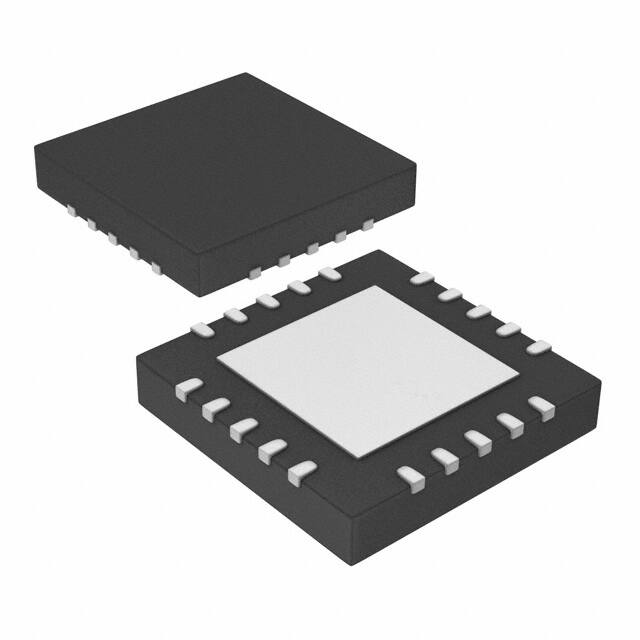


 工商网监
湘ICP备2023018690号
工商网监
湘ICP备2023018690号
