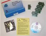
Active Filter Demo Board Kit
User’s Guide
© 2006 Microchip Technology Inc.
DS51614A
�Note the following details of the code protection feature on Microchip devices:
•
Microchip products meet the specification contained in their particular Microchip Data Sheet.
•
Microchip believes that its family of products is one of the most secure families of its kind on the market today, when used in the
intended manner and under normal conditions.
•
There are dishonest and possibly illegal methods used to breach the code protection feature. All of these methods, to our
knowledge, require using the Microchip products in a manner outside the operating specifications contained in Microchip’s Data
Sheets. Most likely, the person doing so is engaged in theft of intellectual property.
•
Microchip is willing to work with the customer who is concerned about the integrity of their code.
•
Neither Microchip nor any other semiconductor manufacturer can guarantee the security of their code. Code protection does not
mean that we are guaranteeing the product as “unbreakable.”
Code protection is constantly evolving. We at Microchip are committed to continuously improving the code protection features of our
products. Attempts to break Microchip’s code protection feature may be a violation of the Digital Millennium Copyright Act. If such acts
allow unauthorized access to your software or other copyrighted work, you may have a right to sue for relief under that Act.
Information contained in this publication regarding device
applications and the like is provided only for your convenience
and may be superseded by updates. It is your responsibility to
ensure that your application meets with your specifications.
MICROCHIP MAKES NO REPRESENTATIONS OR
WARRANTIES OF ANY KIND WHETHER EXPRESS OR
IMPLIED, WRITTEN OR ORAL, STATUTORY OR
OTHERWISE, RELATED TO THE INFORMATION,
INCLUDING BUT NOT LIMITED TO ITS CONDITION,
QUALITY, PERFORMANCE, MERCHANTABILITY OR
FITNESS FOR PURPOSE. Microchip disclaims all liability
arising from this information and its use. Use of Microchip
devices in life support and/or safety applications is entirely at
the buyer’s risk, and the buyer agrees to defend, indemnify and
hold harmless Microchip from any and all damages, claims,
suits, or expenses resulting from such use. No licenses are
conveyed, implicitly or otherwise, under any Microchip
intellectual property rights.
Trademarks
The Microchip name and logo, the Microchip logo, Accuron,
dsPIC, KEELOQ, microID, MPLAB, PIC, PICmicro,
PICSTART, PRO MATE, PowerSmart, rfPIC and SmartShunt
are registered trademarks of Microchip Technology
Incorporated in the U.S.A. and other countries.
AmpLab, FilterLab, Migratable Memory, MXDEV, MXLAB,
SEEVAL, SmartSensor and The Embedded Control Solutions
Company are registered trademarks of Microchip Technology
Incorporated in the U.S.A.
Analog-for-the-Digital Age, Application Maestro, dsPICDEM,
dsPICDEM.net, dsPICworks, ECAN, ECONOMONITOR,
FanSense, FlexROM, fuzzyLAB, In-Circuit Serial
Programming, ICSP, ICEPIC, Linear Active Thermistor, Mindi,
MiWi, MPASM, MPLIB, MPLINK, PICkit, PICDEM,
PICDEM.net, PICLAB, PICtail, PowerCal, PowerInfo,
PowerMate, PowerTool, REAL ICE, rfLAB, rfPICDEM, Select
Mode, Smart Serial, SmartTel, Total Endurance, UNI/O,
WiperLock and ZENA are trademarks of Microchip
Technology Incorporated in the U.S.A. and other countries.
SQTP is a service mark of Microchip Technology Incorporated
in the U.S.A.
All other trademarks mentioned herein are property of their
respective companies.
© 2006, Microchip Technology Incorporated, Printed in the
U.S.A., All Rights Reserved.
Printed on recycled paper.
Microchip received ISO/TS-16949:2002 certification for its worldwide
headquarters, design and wafer fabrication facilities in Chandler and
Tempe, Arizona, Gresham, Oregon and Mountain View, California. The
Company’s quality system processes and procedures are for its
PICmicro® 8-bit MCUs, KEELOQ® code hopping devices, Serial
EEPROMs, microperipherals, nonvolatile memory and analog
products. In addition, Microchip’s quality system for the design and
manufacture of development systems is ISO 9001:2000 certified.
DS51614A-page ii
© 2006 Microchip Technology Inc.
�ACTIVE FILTER DEMO BOARD KIT
USER’S GUIDE
Table of Contents
Preface ........................................................................................................................... 1
Introduction............................................................................................................ 1
Document Layout .................................................................................................. 1
Conventions Used in this Guide ............................................................................ 2
Recommended Reading........................................................................................ 3
The Microchip Web Site ........................................................................................ 3
Customer Support ................................................................................................. 3
Document Revision History ................................................................................... 3
Chapter 1. Product Overview ....................................................................................... 5
1.1 Introduction ..................................................................................................... 5
1.2 Kit Contents .................................................................................................... 5
1.3 Intended Use of the Active Filter Demo Board Kit .......................................... 6
1.4 Active Filter Demo Board Kit Description ....................................................... 6
1.5 Sub-assemblies .............................................................................................. 6
1.6 Associated Tools ............................................................................................ 8
Chapter 2. Setup and Installation ................................................................................ 9
2.1 Introduction ..................................................................................................... 9
2.2 Required Tools ............................................................................................... 9
2.3 Connecting the PCBs ..................................................................................... 9
2.4 VDD/2 Filter Section Set-up .......................................................................... 10
2.5 Active Filter Section Set-up .......................................................................... 11
2.6 Set-up Verification ........................................................................................ 17
Chapter 3. Building the Filter Supplied in the Kit .................................................... 19
3.1 Introduction ................................................................................................... 19
3.2 The Filter Design .......................................................................................... 19
3.3 Putting the Filter Together ............................................................................ 20
3.4 Testing the Filter ........................................................................................... 21
Chapter 4. Common Filter Modifications .................................................................. 25
4.1 Introduction ................................................................................................... 25
4.2 Power Supplies ............................................................................................ 25
4.3 Filter Section Ordering for Noise and Headroom ......................................... 27
4.4 Combining Low-pass and High-pass Sections ............................................. 27
4.5 Higher Frequency Filters .............................................................................. 27
4.6 Using 8-Pin SOIC Op Amps ......................................................................... 28
© 2006 Microchip Technology Inc.
DS51614A-page iii
�Active Filter Demo Board Kit User’s Guide
Appendix A. Schematics and Layouts ......................................................................31
A.1 Introduction .................................................................................................. 31
A.2 VDD/2 Filter Section (Sub-Assembly #: 102-00098R1) ................................ 31
A.3 Active Filter Section (Sub-Assembly #: 102-00097R1) ................................ 34
A.4 Accessory Bag (Sub-Assembly #: 110-00097R1) ........................................ 37
Appendix B. Bill Of Materials (BOM) ..........................................................................39
B.1 VDD/2 Filter Section BOMs .......................................................................... 39
B.2 Active Filter Section BOM ............................................................................ 40
B.3 Accessory Bag BOM .................................................................................... 41
Worldwide Sales and Service .....................................................................................42
DS51614A-page iv
© 2006 Microchip Technology Inc.
�ACTIVE FILTER DEMO BOARD KIT
USER’S GUIDE
Preface
NOTICE TO CUSTOMERS
All documentation becomes dated, and this manual is no exception. Microchip tools and
documentation are constantly evolving to meet customer needs, so some actual dialogs
and/or tool descriptions may differ from those in this document. Please refer to our web site
(www.microchip.com) to obtain the latest documentation available.
Documents are identified with a “DS” number. This number is located on the bottom of each
page, in front of the page number. The numbering convention for the DS number is
“DSXXXXXA”, where “XXXXX” is the document number and “A” is the revision level of the
document.
For the most up-to-date information on development tools, see the MPLAB® IDE on-line help.
Select the Help menu, and then Topics to open a list of available on-line help files.
INTRODUCTION
This chapter contains general information that will be useful to know before using the
Active Filter Demo Board Kit. Items discussed in this chapter include:
•
•
•
•
•
•
Document Layout
Conventions Used in this Guide
Recommended Reading
The Microchip Web Site
Customer Support
Document Revision History
DOCUMENT LAYOUT
This document describes how to use the Active Filter Demo Board Kit. The manual
layout is as follows:
• Chapter 1. “Product Overview” - Important information about the Active Filter
Demo Board Kit.
• Chapter 2. “Setup and Installation” – Covers the initial set-up of the Active
Filter Demo Board Kit. It lists the required tools, shows how to connect the boards
and demonstrates how to verify the set-up.
• Chapter 3. “Building the Filter Supplied in the Kit” – Discusses the filter supplied in the kit (loose parts in a separate bag). Its design, component placement,
and testing are discussed.
• Chapter 4. “Common Filter Modifications” – Covers modifications that are
easy to do with these boards. It also discusses common filter limitations.
• Appendix A. “Schematics and Layouts” – Shows the schematic and board
layouts for the Active Filter Demo Board Kit.
• Appendix B. “Bill Of Materials (BOM)” – Lists the parts used to build the
sub-assemblies in the Active Filter Demo Board Kit.
© 2006 Microchip Technology Inc.
DS51614A-page 1
�Active Filter Demo Board Kit User’s Guide
CONVENTIONS USED IN THIS GUIDE
This manual uses the following documentation conventions:
DOCUMENTATION CONVENTIONS
Description
Arial font:
Italic characters
Represents
Referenced books
Emphasized text
A window
A dialog
A menu selection
A field name in a window or
dialog
A menu path
MPLAB® IDE User’s Guide
...is the only compiler...
the Output window
the Settings dialog
select Enable Programmer
“Save project before build”
A dialog button
A tab
A number in verilog format,
where N is the total number of
digits, R is the radix and n is a
digit.
A key on the keyboard
Click OK
Click the Power tab
4‘b0010, 2‘hF1
Italic Courier New
Sample source code
Filenames
File paths
Keywords
Command-line options
Bit values
Constants
A variable argument
Square brackets [ ]
Optional arguments
Curly brackets and pipe
character: { | }
Ellipses...
Choice of mutually exclusive
arguments; an OR selection
Replaces repeated text
#define START
autoexec.bat
c:\mcc18\h
_asm, _endasm, static
-Opa+, -Opa0, 1
0xFF, ‘A’
file.o, where file can be
any valid filename
mcc18 [options] file
[options]
errorlevel {0|1}
Initial caps
Quotes
Underlined, italic text with
right angle bracket
Bold characters
N‘Rnnnn
Text in angle brackets < >
Courier New font:
Plain Courier New
Represents code supplied by
user
DS51614A-page 2
Examples
File>Save
Press ,
var_name [,
var_name...]
void main (void)
{ ...
}
© 2006 Microchip Technology Inc.
�Preface
RECOMMENDED READING
This user's guide describes how to use Active Filter Demo Board Kit. Other useful
documents are listed below. The following Microchip documents are available and
recommended as supplemental reference resources.
MCP6271 Data Sheet (DS21810)
Gives detailed information on the op amps that are included in the Active Filter Demo
Board Kit Accessory Bag.
FilterLab® 2.0 User’s Guide (DS51419)
Covers the functionality of Microchip’s active filter design software. The appendices
include information on filter terminology, design parameters, selecting an op amp, and
selected references to the analog filter literature.
THE MICROCHIP WEB SITE
Microchip provides online support via our web site at www.microchip.com. This web
site is used as a means to make files and information easily available to customers.
Accessible by using your favorite Internet browser, the web site contains the following
information:
• Product Support – Data sheets and errata, application notes and sample
programs, design resources, user’s guides and hardware support documents,
latest software releases and archived software
• General Technical Support – Frequently Asked Questions (FAQs), technical
support requests, online discussion groups, Microchip consultant program
member listing
• Business of Microchip – Product selector and ordering guides, latest Microchip
press releases, listing of seminars and events, listings of Microchip sales offices,
distributors and factory representatives
CUSTOMER SUPPORT
Users of Microchip products can receive assistance through several channels:
•
•
•
•
•
Distributor or Representative
Local Sales Office
Field Application Engineer (FAE)
Technical Support
Development Systems Information Line
Customers should contact their distributor, representative or field application engineer
for support. Local sales offices are also available to help customers. A listing of sales
offices and locations is included in the back of this document.
Technical support is available through the web site at: http://support.microchip.com
DOCUMENT REVISION HISTORY
Revision A (June 2006)
• Initial Release of this Document.
© 2006 Microchip Technology Inc.
DS51614A-page 3
�Active Filter Demo Board Kit User’s Guide
NOTES:
DS51614A-page 4
© 2006 Microchip Technology Inc.
�ACTIVE FILTER DEMO BOARD KIT
USER’S GUIDE
Chapter 1. Product Overview
1.1
INTRODUCTION
The Active Filter Demo Board Kit is described by the following:
• Assembly # : 114-00097R1
• Order # : MCP6XXXDM-FLTR
• Name: Active Filter Demo Board Kit
Items discussed in this chapter include:
•
•
•
•
•
1.2
Kit Contents
Intended Use of the Active Filter Demo Board Kit
Active Filter Demo Board Kit Description
Sub-Assemblies
Associated Tools
KIT CONTENTS
•
•
•
•
•
VDD/2 Filter Section Board - One partially assembled board
Active Filter Section – Four partially assembled boards
Important Information “Read First”
Accessory Bag - contains loose parts for populating sockets on boards
Analog and Interface Products Demonstration Boards CD-ROM (DS21912) – This
CD-ROM contains the files and literature mentioned in this user’s guide
FIGURE 1-1:
© 2006 Microchip Technology Inc.
Active Filter Demo Board Kit Contents.
DS51614A-page 5
�Active Filter Demo Board Kit User’s Guide
1.3
INTENDED USE OF THE ACTIVE FILTER DEMO BOARD KIT
This kit is intended to support active filters designed by FilterLab® V2.0 (see
Section 1.6 “Associated Tools”). These filters are all pole and are built by cascading
first and second order sections.
Higher frequency filters (e.g., a low-pass filter with cutoff at 1 MHz) can have their
design initially verified on these boards; see Section 4.5 “Higher Frequency Filters”.
1.4
ACTIVE FILTER DEMO BOARD KIT DESCRIPTION
The Printed Circuit Boards (PCB) in the Active Filter Demo Board Kit have the following
features:
• All filter resistors and capacitors are socketed
• Supports all Microchip single op amps
- PDIP-8 package (e.g., MCP6271) are socketed
- SOIC-8 package can be accomodated; see Section 4.6 “Using 8-Pin SOIC
Op Amps”
• Test points for connecting lab equipment
• Single supply configuration
• Modularized connection scheme
1.5
SUB-ASSEMBLIES
The Active Filter Demo Board Kit is comprised of three sub-assemblies:
• VDD/2 Filter Section
- Sub-Assembly # : 102-00098R1
- One PCB designed to provide mid-supply biasing to the other PCBs
- Provides power supply test points for a lab power supply
- Provides input test points for a lab signal generator
• Active Filter Sections
- Sub-Assembly # : 102-00097R1
- Four PCBs designed to be cascaded
- Support filter orders between n = 1 and n = 8
- Provide output test points for lab equipment
• Accessory Bag
- Sub-Assembly # : 110-00097R1
- Kit of resistors, capacitors, and op amps that can be used to build the filter
circuit in Figure 2-8
DS51614A-page 6
© 2006 Microchip Technology Inc.
�Product Overview
Figure 1-2 shows the Active Filter Demo Board Kit’s five PCBs; one VDD/2 Filter
Section PCB and four Active Filter Section PCB’s. It shows how these boards are
cascaded (using board connectors), and how lab equipment can be attached (via test
points) to measure the filter response.
Power Supply
3
3
3
Signal Analyzer
3
3
VDD/2
Filter
Section
3
1st
Active
Filter
Section
3
2nd
3
Active
Filter
Section
3
2
3
3rd
Active
Filter
Section
4th
3
Active
Filter
Section
3
3
2
Signal Generator
FIGURE 1-2:
Measurement Setup Block Diagram.
Figure 1-3 shows the block diagram of the VDD/2 Filter Section, and Figure 1-4 shows
the block diagram of the Active Filter Sections.
VDD
Power
Supply
Input
VDD/2
GND
GND
Signal
Input
VIN
GND
Supply Test Points
Select
VDD/2 Source
(INT or EXT)
Single Op Amp
(buffers the internal
VDD/2 Source)
VDD
Power
Supply
Output
VDD/2
GND
GND
Signal
Output
VOUT
GND
Signal Input
Test Points
FIGURE 1-3:
VDD/2 Filter Section Block Diagram.
VDD
Power
Supply
Input
VDD/2
VIN
GND
FIGURE 1-4:
© 2006 Microchip Technology Inc.
Signal Output
Test Points
GND
GND
Signal
Input
Single
Op Amp
VDD
VDD/2
GND
Resistor and
Capacitor
Sockets
Power
Supply
Output
GND
VOUT
Signal
Output
GND
Active Filter Section (4 each) Block Diagram.
DS51614A-page 7
�Active Filter Demo Board Kit User’s Guide
1.6
ASSOCIATED TOOLS
FilterLab 2.0® is an innovative software tool that simplifies active (op amp) filter design.
Available at no cost from Microchip’s web site (www.microchip.com), the FilterLab 2.0
active filter software design tool provides full schematic diagrams of the filter circuit with
component values, displays the frequency response, and gives a SPICE listing for
further simulations. Users can select a low-pass, band-pass or high-pass response.
Available functions are Bessel, Butterworth, and Chebyshev, with order between n = 1
and 8.
DS51614A-page 8
© 2006 Microchip Technology Inc.
�ACTIVE FILTER DEMO BOARD KIT
USER’S GUIDE
Chapter 2. Setup and Installation
2.1
INTRODUCTION
This chapter shows how to set up the Active Filter Demo Board Kit. Items discussed in
this chapter include:
•
•
•
•
•
2.2
Required Tools
Connecting the PCBs
VDD/2 Filter Section Set-up
Active Filter Section Set-up
Set-up Verification
REQUIRED TOOLS
• Lab power supply
• Lab signal source (e.g., function generator)
• Lab measurement equipment (e.g., oscilloscope)
2.3
CONNECTING THE PCBs
This section discusses the primary method for setting up the Active Filter Demo Board
Kit. An exploded view of how the different boards connect is shown in Figure 2-1 (see
also Figure 1-2).
The filter order will determine how many of the Active Filter Section boards need to be
cascaded (one board when n = 1 or 2, two boards when n = 3 or 4, …).
The board edge connectors are slid together to make good electrical connection
between boards.
The (surface mount) test points allow lab equipment to be connected to these boards.
The user provides the input signal and power to the VDD/2 Filter Section, and measures
the output signal at the last Active Filter Section.
Lab Power Supply
Function Generator
FIGURE 2-1:
© 2006 Microchip Technology Inc.
Oscilloscope
VDD/2 Filter Section
Active Filter Section
Board Connections for the Active Filter Demo Board Kit.
DS51614A-page 9
�Active Filter Demo Board Kit User’s Guide
The user provides the supply voltages, which need to be in the allowed range for the
installed op amps. Any of Microchip’s op amps that operate below 5.5V can be used;
higher voltage parts can be accommodated (see Section 4.2 “Power Supplies”). Five
MCP6271 op amps are included in the accessory bag for convenience.
The power lines are bypassed by 1.0 µF capacitors at each board input. The op amps
also have 0.1 µF local bypass capacitors.
2.4
VDD/2 FILTER SECTION SET-UP
Figure 2-2 gives the circuit diagram for the VDD/2 Filter Section. It allows the mid-supply
voltage (VDD/2) to be set by an external power supply (JP1 at EXT), or internally (JP1
at INT) by the on-board op amp (U1). The headers and test points allow the user
flexibility in setting up a filter circuit.
P1
VDD
TP3
VDD
C1
1.0 µF
VDD/2
C2
1.0 µF
GND
JP1
EXT
TP4
INT
VDD/2
VIN
GND
GND
U1
MCP6271
R2
20 kΩ
GND
C4
0.1 µF
VOUT
TP1
GND
J1
VIN
TP2
VDD
VDD/2
TP5
C3
0.1 µF
R1
20 kΩ
GND
J2
GND
P2
GND
FIGURE 2-2:
VDD/2 Filter Section Circuit.
The VDD/2 Filter Section PCB is shown in Figure 2-3. The single op amp U1 can have
either a PDIP-8 or SOIC-8 package:
• PDIP-8 packages are inserted into the DIP-8 socket above the U1 label
• SOIC-8 packages can be accommodated; see Section 4.6 “Using 8-Pin SOIC
Op Amps”
• Only one op amp can be connected at a time
Select the mid-supply power source by setting jumper JP1 to (see Figure 2-3):
• Internal VDD/2 (INT on bottom)
- Op amp U1 drives the VDD/2 line on all of the PCBs
- The VDD/2 line must be disconnected from any power supply (at P1 or TP4)
• External VDD/2 (EXT on top, as shown)
- Op amp U1 has no load
- The VDD/2 line must be connected to an external supply voltage (at P1 or
TP4)
The headers P1 and J1 on the left of the board are unpopulated (see Figure 2-3):
• The test points TP1 through TP5 provide connections for the same voltages
• P1 and J1 can be populated by the user, if desired, to connect to another (user
provided) board on the left
DS51614A-page 10
© 2006 Microchip Technology Inc.
�Setup and Installation
VDD
VDD/2
VDD
VDD/2
GND
GND
GND
VIN
GND
GND
FIGURE 2-3:
2.5
VOUT
GND
VDD/2 Filter Section Top View.
ACTIVE FILTER SECTION SET-UP
The filter sections designed by FilterLab V2.0 have several topologies. This section
details the conversion of these topologies to the Active Filter Demo Board Kit.
Figure 2-4 shows the circuit diagram for the Active Filter Section.
P1
VDD
J2
C1
1.0 µF
VDD/2
C2
0.1 µF
R1
10Ω
GND
GND
VOUT
TP1
GND
U1
MCP6271
C3
GND
0.1 µF
Z4
Z10
Z9
GND
J1
Z8
Z7
Z6
FIGURE 2-4:
© 2006 Microchip Technology Inc.
GND
TP3
Z11
VIN
VDD/2
VDD/2
TP2
VDD
Z2
Z5
VOUT
GND
Z3
P2
Z1
Active Filter Section Circuit.
DS51614A-page 11
�Active Filter Demo Board Kit User’s Guide
The Active Filter Section is shown in Figure 2-5. The single op amp U1 can have either
a PDIP-8 or SOIC-8 package:
• PDIP-8 packages are inserted into the DIP-8 socket to the right of the U1 label
• SOIC-8 packages can be accommodated; see Section 4.6 “Using 8-Pin SOIC
Op Amps”
The resistors and capacitors that are part of a filter section are placed in pin sockets
(see Figure 2-5):
• The socket pairs are labeled Z1 through Z12
• The following sub-sections detail how the resistors and capacitors are chosen and
populated
VDD
VDD/2
GND
VDD
VDD/2
GND
GND
VIN
GND
GND
VOUT
GND
FIGURE 2-5:
DS51614A-page 12
Active Filter Section Top View.
© 2006 Microchip Technology Inc.
�Setup and Installation
2.5.1
FilterLab Circuit Topology vs. PCB Reference Designators
FilterLab V2.0 labels the capacitors and resistors in its circuit diagram as follows:
• R12 = Resistor, Section # 1, Resistor # 2 in that section
• C31 = Capacitor, Section # 3, Capacitor # 1 in that section
• Ra = Gain setting resistor for op amp in Sallen-Key Section # 1 (open, and not
labeled, when in unity gain)
• Rb = Feedback resistor for op amp in Sallen-Key Section # 1 (0Ω, and not
labeled, when in unity gain)
The resistor and capacitor reference designators on the Active Filter Section board
(Z1 - Z11) need to be filled according to FilterLab’s design. The following sub-sections
show how to convert from FilterLab’s circuit diagram to the PCB.
In the following, the PCBs are given section numbers 0 to 4:
• Section # 0 – for VDD/2 Filter Section
• Section # 1 to # 4 – for cascaded Active Filter Section
The different circuit topologies referred to in Section 2.5.2 “Sallen-Key, Low-pass Filter Sections”, Section 2.5.3 “Sallen-Key, High-pass Filter Sections”, and
Section 2.5.4 “Multiple Feedback, Low-pass and Band-pass Filter Sections” will
be labeled as shown in Figure 2-6.
AAA-BB#-C
AAA:
SK = Sallen-Key
MFB = Multiple Feedback
BB:
LP = Low-pass
BP = Band-pass
HP = High-pass
#:
1 = Single, Real Pole
2 = Double, Complex Poles
C:
“blank” = Sallen-Key Unity Gain Buffer (K = 1)
or Multiple Feedback
K = Sallen-Key Non-unity Gain Amplifier (K > 1)
FIGURE 2-6:
© 2006 Microchip Technology Inc.
Filter Section Labels.
DS51614A-page 13
�Active Filter Demo Board Kit User’s Guide
2.5.2
Sallen-Key, Low-pass Filter Sections
TABLE 2-1:
IMPEDANCES FOR SALLEN-KEY, LOW-PASS FILTER
SECTIONS
Topology
SK-LP1
SK-LP2
SK-LP1-K
SK-LP2-K
Z1
0Ω
R11
0Ω
R11
Z2
R11
R12
R11
R12
Z3
—
C11
—
C11
Z4
—
—
—
—
Z5
C11
C12
C11
C12
Z6
—
—
—
—
Z7
—
—
0Ω
0Ω
Z8
—
—
—
—
Z9
—
—
—
—
Z10
—
—
Ra
Ra
Z11
0Ω
0Ω
Rb
Rb
SK-LP1
VIN
R11
SK-LP2
VDD
C11
U1
C11
VOUT
VIN
R11
R12
VDD
U1
C12
SK-LP1-K
VIN
R11
SK-LP2-K
VDD
C11
U1
C11
VOUT
VIN
R11
R12
VDD
U1
C12
VDD/2
Ra
FIGURE 2-7:
DS51614A-page 14
Rb
VOUT
VDD/2
Ra
VOUT
Rb
Sallen-Key, Low-pass (modified) Filter Topologies.
© 2006 Microchip Technology Inc.
�Setup and Installation
2.5.3
Sallen-Key, High-pass Filter Sections
TABLE 2-2:
IMPEDANCES FOR SALLEN-KEY, HIGH-PASS FILTER
SECTIONS
Topology
SK-HP1
SK-HP2
SK-HP1-K
SK-HP2-K
Z1
0Ω
C11
0Ω
C11
Z2
C11
C12
C11
C12
Z3
—
R11
—
R11
Z4
R11
R12
R11
R12
Z5
—
—
—
—
Z6
—
—
—
—
Z7
—
—
0Ω
0Ω
Z8
—
—
—
—
Z9
—
—
—
—
Z10
—
—
Ra
Ra
Z11
0Ω
0Ω
Rb
Rb
SK-HP1
C11
VIN
SK-HP2
R11
VDD
U1
VOUT
R11
VIN
C11
VDD/2
U1
R11
SK-HP2-K
VOUT
VIN
Ra
R11
C11
Rb
© 2006 Microchip Technology Inc.
VDD
C12
U1
VOUT
R12
VDD/2
FIGURE 2-8:
VOUT
VDD/2
VDD
C11
VDD/2
U1
R12
SK-HP1-K
VIN
VDD
C12
Ra
Rb
Sallen-Key, High-pass (modified) Filter Topologies.
DS51614A-page 15
�Active Filter Demo Board Kit User’s Guide
2.5.4
Multiple Feedback, Low-pass and Band-pass Filter Sections
TABLE 2-3:
IMPEDANCES FOR MULTIPLE FEEDBACK, LOW-PASS AND
BAND-PASS FILTER SECTIONS
Topology
MFB-LP1
MFB-LP2
MFB-BP2
Z1
—
—
—
Z2
—
—
—
Z3
—
—
—
Z4
0Ω
0Ω
0Ω
Z5
—
—
—
Z6
R11
R11
R11
Z7
—
—
R12
Z8
—
C12
—
Z9
R12
R12
C11
Z10
0Ω
R13
C12
Z11
C11
C11
R13
MFB-LP1
MFB-LP2
C11
R12
R12
VIN
R11
VDD/2
VIN
VDD
C11
R11
R13
VDD
U1
C12
U1
VOUT
VOUT
VDD/2
MFB-BP2
C11
VIN
R13
C12
R11
VDD
U1
R12
VOUT
VDD/2
FIGURE 2-9:
Topologies.
DS51614A-page 16
Multiple Feedback, Low-pass and Band-pass (modified) Filter
© 2006 Microchip Technology Inc.
�Setup and Installation
2.6
SET-UP VERIFICATION
1. Install components (resistors, capacitors, and op amps) for a filter design (e.g.,
the filter described in Section 3.2 “The Filter Design” and
Section 3.3 “Putting the Filter Together”).
2. Verify the power supply voltages, including VDD/2, for all of the boards.
3. Test the filter response as described in Section 3.4 “Testing the Filter”.
© 2006 Microchip Technology Inc.
DS51614A-page 17
�Active Filter Demo Board Kit User’s Guide
NOTES:
DS51614A-page 18
© 2006 Microchip Technology Inc.
�ACTIVE FILTER DEMO BOARD KIT
USER’S GUIDE
Chapter 3. Building the Filter Supplied in the Kit
3.1
INTRODUCTION
The accessory bag that comes with this kit makes it quick and easy to evaluate the filter
described below; it was designed in FilterLab V2.0. Items discussed in this chapter
include:
• The Filter Design
• Putting the Filter Together
• Testing the Filter
3.2
THE FILTER DESIGN
See Figure 3-1 for the circuit diagram supported by the accessory bag. This filter is
described as follows:
•
•
•
•
•
•
Bessel Low-pass
n = 5, (filter order)
fC = 100 Hz, (cut-off frequency)
Gain = 1 V/V
Sallen-Key sections
Single Supply
SK-LP2
SK-LP1
SK-LP2
C21
VIN
R11
R21
10.7k
C11
0.10µ
3.16k
U1
MCP6271
FIGURE 3-1:
Demo Board Kit.
C31
0.39µ
R22
R31
6.81k
C22
0.10µ
5.62k
U2
MCP6271
0.15µ
R32
12.7k
C32
0.10µ
VOUT
U3
MCP6271
5th Order, Bessel, Low-pass Filter Supported by the Active Filter
This filter was built, and its frequency response was measured; the result is shown in
Figure 3-2. MCP601 op amps were used, instead of MCP6271 op amps, because they
are slower. Notice how close the measured and simulated data are; this happened
because the MCP601 op amp is much faster than the filter, and because 1% resistors
and 5% capacitors were used.
© 2006 Microchip Technology Inc.
DS51614A-page 19
�Active Filter Demo Board Kit User’s Guide
0
-10
Gain (dB)
-20
Measured
-30
Nominal Simulation
-40
-50
-60
-70
MCP601 Op Amps
-80
10
FIGURE 3-2:
3.3
100
Frequency (Hz)
1,000
Filter Frequency Response.
PUTTING THE FILTER TOGETHER
Each of the components in Figure 3-1 that needs to be inserted in a socket is listed in
Table 3-1 (see Table B-5). This table gives the section number (see
Section 2.5 “Active Filter Section Set-up”) and the PCB reference designators (e.g.,
Z5). Since this design is of 5th order, there are no components for Section # 4.
TABLE 3-1:
ACCESSORY BAG PARTS LIST
Component Values
Qty
Section
Reference
PCB Label
1
1
C11
Z5
1
2
C22
Z5
1
3
C32
Z5
150 nF
1
3
C31
Z3
390 nF
1
2
C21
Z3
Jumper Wire (0Ω) (Note 1)
2
1
—
Z1, Z11
1
2
—
Z11
100 nF
1
3
—
Z11
3.16 kΩ
1
2
R21
Z1
5.62 kΩ
1
3
R31
Z1
6.81 kΩ
1
2
R22
Z2
10.7 kΩ
1
1
R11
Z2
12.7 kΩ
1
3
R32
Z2
MCP6271, Single Op Amp, 2 MHz,
PDIP-8, Microchip Technology Inc.
(Note 1)
1
0
U1
U1
1
1
U1
U1
1
2
U2
U1
1
3
U3
U1
Note 1:
DS51614A-page 20
The other 6 jumpers and 1 op amp in the accessory bag are for convenience in
building other filters.
© 2006 Microchip Technology Inc.
�Building the Filter Supplied in the Kit
Figure 3-3 is a picture of the fully assembled filter shown in Figure 3-1. Note that the
board on the left (VDD/2 Filter Section) provides an easy way to connect the input signal
source and power supply to the filter. JP1 on this board may be connected to INT or
EXT in this case.
FIGURE 3-3:
Kit.
3.4
Picture of the Filter Supported by the Active Filter Demo Board
TESTING THE FILTER
3.4.1
DC Bias
Figure 3-4 shows the most important DC bias voltages to check.
Test VOUT Here
Test Supply Voltages Here
VDD
VDD/2
GND
VDD
VDD/2
GND
VIN
GND
GND
VOUT
GND
GND
FIGURE 3-4:
3.4.2
Points to check DC Bias.
Response Variability
Resistors and capacitors with tighter tolerances will reduce the variability of the filters
response over process and, sometimes, temperature. Figure 3-5 shows the simulated
±3.3 sigma gain error (in dB) for each frequency (based on a uniform random
distribution). Figure 3-6 shows a histogram of the pass-band frequency (fP) from the
same simulation.
© 2006 Microchip Technology Inc.
DS51614A-page 21
�Gain Spread (dB)
Active Filter Demo Board Kit User’s Guide
2.5
2.0
1.5
1.0
0.5
0.0
-0.5
-1.0
-1.5
-2.0
-2.5
100 MC Sims
1% R's
5% C's
-3.3 sigma
10
100
Frequency (Hz)
1,000
Gain Error (Monte Carlo simulation) vs. Frequency.
110
108
106
104
102
100
98
96
94
100 MC Sims
1% R's
5% C's
92
26%
24%
22%
20%
18%
16%
14%
12%
10%
8%
6%
4%
2%
0%
90
Percentage of Occurrences
FIGURE 3-5:
+3.3 sigma
Pass-Band Frequency at -3.01 dB (Hz)
FIGURE 3-6:
Pass-Band Frequency (Monte Carlo simulation) Histogram.
Using components with tighter tolerances (e.g., 2% capacitors) will improve the
variability of the filter response. This is especially important for filters with a sharp cutoff
characteristic (i.e., Chebyshev).
3.4.3
Checking Output Headroom
It is also possible to check op amp overdrive issues by testing the output of all of the
op amps (every Active Filter Section). The worst-case signal(s) needs to be applied at
the first input. Figure 3-7 shows the frequency response of the filter in Figure 3-1. None
of the traces goes above 0 dB, so this filter should not have output voltage range issues
when the input is a sinewave.
DS51614A-page 22
© 2006 Microchip Technology Inc.
�Building the Filter Supplied in the Kit
0
-10
Gain (dB)
-20
-30
VOUT:
U1
U2
U3
-40
-50
-60
MCP601 Op Amps
Nominal Simulation
-70
-80
10
FIGURE 3-7:
100
Frequency (Hz)
1,000
Frequency Response for All Outputs.
Figure 3-8 shows the step response of the filter in Figure 3-1. The output of U2 (the
second op amp) shows the largest overshoot, so it limits the output voltage range of
the filter. The nominal overshoot is 6.1% (0.18V for a 3.0V step).
Section Output Voltages (V)
4.5
VIN
4.0
VOUT:
U1
U2
U3
3.5
3.0
2.5
2.0
MCP601 Op Amps
Nominal Simulation
VDD = 5.0V
1.5
1.0
0
FIGURE 3-8:
2
4
6
8
Time (ms)
10
12
14
Step Response for All Outputs.
Many SPICE simulators support Monte Carlo simulations. Using this capability on your
design will help determine what tolerances are needed on your design. The same
results can be obtained by measuring many filters (i.e., 30 to 10,000), but at a greater
cost.
© 2006 Microchip Technology Inc.
DS51614A-page 23
�Active Filter Demo Board Kit User’s Guide
NOTES:
DS51614A-page 24
© 2006 Microchip Technology Inc.
�ACTIVE FILTER DEMO BOARD KIT
USER’S GUIDE
Chapter 4. Common Filter Modifications
4.1
INTRODUCTION
The modifications described in this chapter include:
•
•
•
•
•
4.2
Power Supplies
Filter Section Ordering for Noise and Headroom
Combining Low-pass and High-pass Sections
Higher Frequency Filters
Using 8-Pin SOIC Op Amps
POWER SUPPLIES
4.2.1
Dual Power Supplies
To implement dual supplies, change the VDD/2 Filter Section (see Figure 4-1) setup:
• The boards’ bypass capacitors (C1 and C3) need to be removed and replaced
- Connect one set from –VS (board GND) to GND (board VDD/2)
- Connect the other set from +VS (board VDD) to GND (board VDD/2).
• Remove R1 and R2, and then replace R2 with a short
• Set JP1 to External VDD/2 (EXT, as shown)
• Connect the Lab Power Supply
- Voltage +VS to the board’s VDD input (TP3)
- Voltage GND to the VDD/2 input (TP4)
- Voltage –VS to the board’s GND input (TP5)
+VS
Set JP1 to
External (EXT)
–VS
GND
Lab Power Supply
VDD
VDD/2
GND
VDD
VDD/2
GND
GND
VIN
GND
GND
VOUT
GND
These signals correspond
to the pins of the
unpopulated P1 and J1
FIGURE 4-1:
© 2006 Microchip Technology Inc.
Setting up VDD/2 Filter Section for dual supplies.
DS51614A-page 25
�Active Filter Demo Board Kit User’s Guide
To implement dual supplies, it is also necessary to change the Active Filter Section
(see Figure 4-2) set-up:
• The boards’ bypass capacitors (C1 and C3) need to be removed and replaced
- Connect one set from –VS (board GND) to GND (board VDD/2)
- Connect the other set from +VS (board VDD) to GND (board VDD/2).
• If desired, R1 and C1 can be removed
• Connect the Oscilloscope as follows
- Oscilloscope signal probe to VOUT (TP1)
- Oscilloscope GND probe to VDD/2 (TP3)
Note:
Do not connect the oscilloscope GND probe to board GND (TP2) when set
up for dual supplies; this may cause a ground conflict between lab
equipment.
Do not connect
ground probe to GND
Oscilloscope
VOUT
GND
VDD
VDD/2
GND
VDD
VDD/2
GND
GND
VIN
GND
GND
VOUT
GND
FIGURE 4-2:
Setting up Active Filter Section” or dual supplies.
Using dual supplies may not work well for high frequency designs. –VS will be
connected to the ground plane, instead of GND, causing greater radiation of supply
noise and more crosstalk.
4.2.2
Increased Power Supply Voltages
The total voltage across the power supplies should not exceed the op amp’s
specification (5.5V for the MCP6271). The large bypass capacitors on each board are
rated at 16V, which also limits the possible supply voltage.
If necessary, op amps with higher supply voltage can be accommodated. The boards’
bypass capacitors must be removed and replaced with other bypass capacitors with a
higher voltage rating.
DS51614A-page 26
© 2006 Microchip Technology Inc.
�Common Filter Modifications
4.3
FILTER SECTION ORDERING FOR NOISE AND HEADROOM
FilterLab V2.0 orders the filter sections for good dynamic range performance. Its
default selections are:
• Section pole quality factors (QP) are ordered from lowest to highest (from
Section # 1 to Section # 4)
- In other words, section damping factors (ζ = 0.5/QP) go from highest to lowest
(from Section # 1 to Section # 4)
• Gains greater than unity are placed in Section # 1 (for best component
sensitivities)
Some applications may need to alter the default section ordering for special
requirements. To compare different section orderings:
• Check the output headroom of each section’s output (VOUT) using the worst-case
input signal; examples include:
- Minimum and maximum DC levels
- Swept frequency sine wave with maximum magnitude
- Voltage step with maximum step size
• Measure the noise performance
- Measure the output with a DC input signal (i.e., at mid-supply), an
oscilloscope, and a high gain low noise amplifier
- Calculate the standard deviation of the output; this is the integrated noise in
VRMS
- The noise can be improved by scaling the resistors, or by changing the op
amps
• Re-connect the sections in a different order
- Usually it is best to leave the high gain section at the front of the filter
- Re-check output headroom and noise
4.4
COMBINING LOW-PASS AND HIGH-PASS SECTIONS
Some band-pass and band reject filters can be implemented using cascaded low-pass
and high-pass filter sections. These filters have their pass-band frequencies (fPL and
fPH) far apart (e.g., fPH/fPL > 5.8). The low-pass and high-pass filters are usually
designed separately, then cascaded together.
The Active Filter Demo Board Kit allows the user to try out these filters on the bench
with little effort. They also help debug this type of design.
4.5
HIGHER FREQUENCY FILTERS
Higher frequency filters (e.g., a low-pass filter with pass band edge at 1 MHz) can have
their design initially verified on these boards. Simply scale either the resistors or capacitors to a lower frequency design:
• Increase resistors (or capacitors) by a power of 10
• Choose an op amp that is slower by the same power of 10
• Evaluate response:
- All frequency parameters are divided by the same power of 10
- All time parameters are multiplied by the same power of 10
For example, a low-pass filter with a pass-bandfrequency of 1 MHz could be scaled
back to 10 kHz.
The final design must be evaluated on a board capable of supporting higher frequency
signals.
© 2006 Microchip Technology Inc.
DS51614A-page 27
�Active Filter Demo Board Kit User’s Guide
4.6
USING 8-PIN SOIC OP AMPS
There are two options available when using single op amps in SOIC-8 packages (150
mil wide); soldering onto the VDD/2 Filter Section and/or Active Filter Section board(s)
or soldering it onto a separate board which is connected to the DIP-8 socket.
Note:
The DIP-8 socket must be empty; only one op amp can be used at a time.
Figure 4-3 shows a SOIC-8 op amp soldered onto the Active Filter Section Board.
FIGURE 4-3:
Board.
Op Amp in SOIC-8 package soldered onto Active Filter Section
Figure 4-4 shows a SOIC-8 op amp and a DIP-8 socket, soldered onto the 8-Pin
SOIC/MSOP/TSSOP/DIP Evaluation Board available from Microchip Technology Inc
(order # SOIC8EV). The two interconnect strips on the bottom are Samtec part #
BBS-14-T-B or equivalent and are soldered into the through holes for the DIP-8 socket.
Figure 4-5 shows this board plugged into the Active Filter Section Board.
Note:
Insert the interconnect strips into the DIP-8 socket on the VDD/2 Filter Section or Active Filter Section board. Place the SOIC8EV board on the top of
the interconnect strips with the same pin orientation. Now solder the strips
to the top board; this procedure ensures correct alignment of the strips. Clip
the pins flush with the top surface of the SOIC8EV board, then solder the
SOIC-8 op amp on the top.
(Front View)
FIGURE 4-4:
DS51614A-page 28
(Back View)
Op Amp in SOIC-8 package soldered to a separate board.
© 2006 Microchip Technology Inc.
�Common Filter Modifications
FIGURE 4-5:
© 2006 Microchip Technology Inc.
Connecting Adaptor Board onto Active Filter Section.
DS51614A-page 29
�Active Filter Demo Board Kit User’s Guide
NOTES:
DS51614A-page 30
© 2006 Microchip Technology Inc.
�ACTIVE FILTER DEMO BOARD KIT
USER’S GUIDE
Appendix A. Schematics and Layouts
A.1
INTRODUCTION
This appendix contains the schematics and layouts for the different pieces of the Active
Filter Demo Board Kit Sub-assemblies:
• VDD/2 Filter Section (Sub-Assembly # : 102-00098R1)
• Active Filter Section (Sub-Assembly # : 102-00097R1)
• Accessory Bag (Sub-Assembly # : 110-00097R1)
A.2
VDD/2 FILTER SECTION (SUB-ASSEMBLY #: 102-00098R1)
A.2.1
Circuit
See Figure A-1 for the VDD/2 Filter Section circuit diagram. The input and output
headers (J1, J2, P1, and P2) allow the PCBs to be cascaded as needed. The filter order
will determine how many of the Active Filter Section boards need to be cascaded.
R1, R2, and C3 produce a VDD/2 reference voltage. The op amp U1 buffers this
reference voltage, and is set to unity gain. U1 must drive the impedances connected to
it on all of the Active Filter Section. Op amp U1 is usually a single, PDIP-8 part inserted
into the DIP-8 socket; it can be a SOIC-8 that is soldered to the board (see U1A in
Figure A-1).
C1 and C2 are bypass capacitors for VDD.
The demonstration board includes five test points for convenience on the bench. TP1
and TP2 make it possible to connect a function generator to the filter input; this signal
is passed on to the other boards. TP3 through TP5 provide connections for external
power supplies, which are also passed on to the other boards.
JP1 allows the user to choose the VDD/2 reference voltage source:
• A lab supply (EXT = External VDD/2 source)
• Op amp U1’s output (INT = Internal VDD/2 source)
See Section B.1 “VDD/2 Filter Section BOMs” for the Bill of Material for this kit.
© 2006 Microchip Technology Inc.
DS51614A-page 31
�M
Active Filter Demo Board Kit User’s Guide
FIGURE A-1:
DS51614A-page 32
VDD/2 Filter Section – Schematic.
© 2006 Microchip Technology Inc.
�Schematics and Layouts
A.2.2
Board Plots
The Gerber files for this board are available on the Microchip website
(www.microchip.com) and are contained in the zip file “00098R1 Gerbers.zip”.
FIGURE A-2:
VDD/2 Filter Section – Top Silk Screen.
FIGURE A-3:
VDD/2 Filter Section – Top Metal Layer.
© 2006 Microchip Technology Inc.
DS51614A-page 33
�Active Filter Demo Board Kit User’s Guide
FIGURE A-4:
A.3
VDD/2 Filter Section – Bottom Metal Layer.
ACTIVE FILTER SECTION (SUB-ASSEMBLY #: 102-00097R1)
A.3.1
Circuit
See Figure A-5 for the VDD/2 Filter Sections circuit diagram. The input and output
headers (J1, J2, P1, and P2) allow the PCBs to be cascaded as needed. The filter order
will determine how many of these boards need to be cascaded.
The impedances Z1 to Z11 are realized as resistors, capacitors, shorts or open circuits,
depending on the section topology. These components are placed in pin sockets.
Op amp U1 interacts with the impedances Z1 to Z11 to form an active filter section (one
or two pole). Op amp U1 is usually a single, PDIP-8 part inserted into the DIP-8 socket;
it can be a SOIC-8 that is soldered to the board (see U1A in Figure A-5).
C1 and C3 are bypass capacitors for VDD. C2 is a bypass capacitor for VDD/2, and R1
is a snubber resistor that helps prevent capacitive loading problems for the op amp on
the VDD/2 Filter Section.
The demonstration board includes test points for convenience on the bench. TP1
through TP3 make it possible to measure the output voltage of each filter section.
See Section B.1 “VDD/2 Filter Section BOMs” for the Bill of Material for this kit.
DS51614A-page 34
© 2006 Microchip Technology Inc.
�M
Schematics and Layouts
FIGURE A-5:
Active Filter Section – Schematic.
© 2006 Microchip Technology Inc.
DS51614A-page 35
�Active Filter Demo Board Kit User’s Guide
A.3.2
Board Plots
The Gerber files for this board are available on the Microchip website
(www.microchip.com) and are contained in the zip file “00097R1 Gerbers.zip”.
DS51614A-page 36
FIGURE A-6:
Active Filter Section – Top Silk-Screen.
FIGURE A-7:
Active Filter Section – Top Metal Layer.
© 2006 Microchip Technology Inc.
�Schematics and Layouts
FIGURE A-8:
A.4
Active Filter Section – Bottom Metal Layer.
ACCESSORY BAG (SUB-ASSEMBLY #: 110-00097R1)
See Figure 3-1 for the circuit diagram supported by this Accessory Bag. This filter is a
Bessel low-pass with n = 5, fC = 100 Hz, and Gain = 1 V/V. It uses single supply,
Sallen-Key sections.
See Section B.3 “Accessory Bag BOM” for the Bill of Material for this filter. These
components are placed in an ESD separate ESD bag. The Accessory Bag includes
more MCP6271 op amps than needed for Figure 3-1; there are enough to populate all
of the DIP-8 sockets in the Active Filter Demo Board Kit. These op amps are included
in the accessory bag for ESD protection.
© 2006 Microchip Technology Inc.
DS51614A-page 37
�Active Filter Demo Board Kit User’s Guide
NOTES:
DS51614A-page 38
© 2006 Microchip Technology Inc.
�ACTIVE FILTER DEMO BOARD KIT
USER’S GUIDE
Appendix B. Bill Of Materials (BOM)
B.1
VDD/2 FILTER SECTION BOMS
The BOM in Table B-1 corresponds to Figure 2-2. Unpopulated parts are in Table B-2.
TABLE B-1:
BILL OF MATERIALS (102-00098R1)
Qty Reference
Description
Manufacturer
Part Number
®
2
C3, C4
100 nF, 50V, 10%, X7R,
0805 SMD, Ceramic
Kemet
Electronics
C0805C104K5RACTU
2
C1, C2
1.0 µF, 16V, 10%, X7R,
0805 SMD, Ceramic
Kemet
Electronics
C0805C105K4RACTU
1
JP1
Header, 2 × 2, 0.100" Pitch,
Vertical, Gold
Amp®/Tyco®
Electronics
87227-2
1
(for JP1)
Shunt, 1 × 2, With Handle, Gold
AMP/Tyco
Electronics
881545-2
1
J2
Header, Male, 1 × 3, 0.100",
R/A, Tin
AMP/Tyco
Electronics
640453-3
1
P2
Header, Female, 1 × 3, 0.100",
R/A, Tin
Mill-Max®
801-44-003-20-001000
2
R1, R2
20.0 kΩ, 1/8W, 1%, 0805 SMD
Yageo®
America
RC0805FR-0720KL
5
TP1 – TP5
PC Test Point, Compact,
Surface Mount
Keystone
Electronics
5016
1
(for U1)
IC Socket, 8-pin DIP, Tin, 0.300"
AMP/Tyco
Electronics
2-641260-1
1
PCB
RoHS Compliant Bare PCB,
VDD/2 Filter Section
(1.0 in × 2.0 in)
—
104-00098R1
Note 1:
The components listed in this Bill of Materials are representative of the PCB
assembly. The released BOM used in manufacturing uses all RoHS-compliant
components.
TABLE B-2:
Reference
BILL OF MATERIALS – UNPOPULATED PARTS (102-00098R1)
Description
Manufacturer
Part Number
J1
Header, Male, 1 × 3, 0.100",
R/A, Tin (Note 1)
AMP/Tyco
Electronics
640453-3
P1
Header, Female, 1 × 3, 0.100",
R/A, Tin (Note 1)
Mill-Max®
801-44-003-20-001000
U1
MCP6271, Single Op Amp, 2 MHz,
PDIP-8 (Note 2)
Microchip
MCP6271-E/P
Technology Inc
SOIC-8 (Note 3)
Microchip
MCP6271-E/SN
Technology Inc
Note 1:
2:
3:
© 2006 Microchip Technology Inc.
These parts are supplied by the user, if desired.
This op amp is supplied by Microchip; it is found in the Accessory Bag described in
Table B-5. Any other op amp is supplied by the user.
Op amps in SOIC-8 package are supplied by the user, if desired. See ”4.6 “Using
8-Pin SOIC Op Amps” for information on using op amps in these packages (150
mil wide).
DS51614A-page 39
�Active Filter Demo Board Kit User’s Guide
B.2
ACTIVE FILTER SECTION BOM
The BOM in Table B-3 corresponds to the circuit in Figure 2-4, which is repeated four
times. Unpopulated parts are in Table B-4.
TABLE B-3:
BILL OF MATERIALS (102-00097R1) (NOTE 3)
Qty
Referenc
(Note 1)
e
Manufacturer
Part Number
8
C2, C3
100 nF, 50V, 10%, X7R,
0805 SMD, Ceramic
Kemet
Electronics
C0805C104K5RACTU
4
C1
1.0 µF, 16V, 10%, X7R,
0805 SMD, Ceramic
Kemet
Electronics
C0805C105K4RACTU
8
J1, J2
Header, Male, 1 × 3, 0.100",
R/A, Tin
AMP/Tyco
Electronics
640453-3
8
P1, P2
Header, Female, 1 × 3, 0.100", Mill-Max®
R/A, Tin
801-44-003-20-001000
4
R1
10.0Ω, 1/8W, 1%, 0805 SMD
Yageo America
RC0805FR-0710RL
12
TP1 – TP3 PC Test Point, Compact,
Surface Mount
Keystone
Electronics
5016
4
(for U1)
IC Socket, 8-pin DIP, Tin,
0.300"
AMP/TycoElectronics
2-641260-1
88
(for Z1
to Z11)
Pin Recepticle, 0.015” to
0.025” dia., 0.057” hole dia.
Mill-Max®
(Note 2)
0252-0-15-15-30-27-10-0
4
PCB
RoHS Compliant Bare PCB,
Active Filter Section
(2.0 in × 2.0 in)
—
104-00097R1
Note 1:
2:
3:
The quantities per board all have been multiplied by 4 because there are four Active
Filter Section PCB’s (sub-assembly) in the Active Filter Demo Board Kit (assembly).
This part is also found at Digi-Key (ED90069-ND).
The components listed in this Bill of Materials are representative of the PCB
assembly. The released BOM used in manufacturing uses all RoHS-compliant
components.
TABLE B-4:
Reference
U1
Z1 – Z11
Note 1:
2:
3:
DS51614A-page 40
Description
BILL OF MATERIALS – UNPOPULATED PARTS (102-00097R1)
Description
Manufacturer
Part Number
MCP6271, Single Op Amp, 2 MHz,
PDIP-8 (Note 1)
Microchip
Technology Inc
MCP6271-E/P
SOIC-8 (Note 2)
Microchip
Technology Inc
MCP6271-E/SN
Impedances (resistors and capacitors)
(Note 3)
—
—
These op amps are supplied by Microchip; they are found in the Accessory Bag
described in Table B-5. Other op amps are supplied by the user.
Op amps in SOIC-8 package are supplied by the user, if desired. See ”4.6 “Using
8-Pin SOIC Op Amps” for information on using op amps in these packages (150
mil wide).
The resistors and capacitors represented by Z1 to Z11 are provided by the
customer. Not all of these will be populated for any given filter. The Accessory Bag
described in Table B-5 includes 10 jumpers that can be used to configure different
filter circuits.
© 2006 Microchip Technology Inc.
�Bill Of Materials (BOM)
B.3
ACCESSORY BAG BOM
The BOM in Table B-5 corresponds to the collection of resistors, capacitors, and
MCP6271 op amps that comes in the Accessory Bag which is shipped in the Active
Filter Demo Board Kit. It includes enough op amps and jumpers to support any
reasonable filter design. It also supports the circuit in ”Chapter 3. “Building the Filter
Supplied in the Kit”. Other filters may need tighter tolerance resistors and capacitors
(i.e., 1% or 2%). The customer provides the resistors and capacitors for any other filter
circuit.
TABLE B-5:
Qty
BILL OF MATERIALS (110-00097R1)
Reference
Description
Manufacturer
Part Number
3
C11, C22, C32
100 nF, 50V, 5%, Radial,
Polyester Film
Panasonic
ECQ-B1H104JF
1
C31
150 nF, 50V, 5%, Radial,
Polyester Film
Panasonic
ECQ-B1H154JF
1
C21
390 nF, 50V, 5%, Radial,
Polyester Film
Panasonic
ECQ-B1H394JF
10
—
Jumper Wire, 0Ω, Axial
1/8W Resistor” (Note 1)
Yageo America ZOR-12-B-52
1
R21
3.16 kΩ, 1/4W, 1%, Axial,
Metal Film
Yageo America MFR-25FBF-3K16
1
R31
5.62 kΩ, 1/4W, 1%, Axial,
Metal Film
Yageo America MFR-25FBF-5K62
1
R22
6.81 kΩ, 1/4W, 1%, Axial,
Metal Film
Yageo America MFR-25FBF-6K81
1
R11
10.7 kΩ, 1/4W, 1%, Axial,
Metal Film
Yageo America MFR-25FBF-10K7
1
R32
12.7 kΩ, 1/4W, 1%, Axial,
Metal Film
Yageo America MFR-25FBF-12K7
5
U1
MCP6271, Single Op Amp,
2 MHz, PDIP-8 (Note 2)
Microchip
Technology Inc
Note 1:
2:
© 2006 Microchip Technology Inc.
MCP6271-E/P
Four of these “resistors” (jumpers) are used for shorting the feedback resistors (Z1
on 3 PCBs), and for shorting Z11 on the SK-LP1 stage (see Table 3-1), for the filter
in ”Chapter 3. “Building the Filter Supplied in the Kit”. A total of ten is
included because this is the maximum that might be needed for any FilterLab
design, plus two spares.
These five op amps are placed in ESD protective “clam shells,” which are then put
into an ESD protective bag with the resistors and capacitors.
DS51614A-page 41
�WORLDWIDE SALES AND SERVICE
AMERICAS
ASIA/PACIFIC
ASIA/PACIFIC
EUROPE
Corporate Office
2355 West Chandler Blvd.
Chandler, AZ 85224-6199
Tel: 480-792-7200
Fax: 480-792-7277
Technical Support:
http://support.microchip.com
Web Address:
www.microchip.com
Australia - Sydney
Tel: 61-2-9868-6733
Fax: 61-2-9868-6755
India - Bangalore
Tel: 91-80-4182-8400
Fax: 91-80-4182-8422
China - Beijing
Tel: 86-10-8528-2100
Fax: 86-10-8528-2104
India - New Delhi
Tel: 91-11-5160-8631
Fax: 91-11-5160-8632
Austria - Wels
Tel: 43-7242-2244-3910
Fax: 43-7242-2244-393
Denmark - Copenhagen
Tel: 45-4450-2828
Fax: 45-4485-2829
China - Chengdu
Tel: 86-28-8676-6200
Fax: 86-28-8676-6599
India - Pune
Tel: 91-20-2566-1512
Fax: 91-20-2566-1513
France - Paris
Tel: 33-1-69-53-63-20
Fax: 33-1-69-30-90-79
China - Fuzhou
Tel: 86-591-8750-3506
Fax: 86-591-8750-3521
Japan - Yokohama
Tel: 81-45-471- 6166
Fax: 81-45-471-6122
Germany - Munich
Tel: 49-89-627-144-0
Fax: 49-89-627-144-44
China - Hong Kong SAR
Tel: 852-2401-1200
Fax: 852-2401-3431
Korea - Gumi
Tel: 82-54-473-4301
Fax: 82-54-473-4302
China - Qingdao
Tel: 86-532-8502-7355
Fax: 86-532-8502-7205
Korea - Seoul
Tel: 82-2-554-7200
Fax: 82-2-558-5932 or
82-2-558-5934
Asia Pacific Office
Suites 3707-14, 37th Floor
Tower 6, The Gateway
Habour City, Kowloon
Hong Kong
Tel: 852-2401-1200
Fax: 852-2401-3431
Atlanta
Alpharetta, GA
Tel: 770-640-0034
Fax: 770-640-0307
Boston
Westborough, MA
Tel: 774-760-0087
Fax: 774-760-0088
Chicago
Itasca, IL
Tel: 630-285-0071
Fax: 630-285-0075
Dallas
Addison, TX
Tel: 972-818-7423
Fax: 972-818-2924
Detroit
Farmington Hills, MI
Tel: 248-538-2250
Fax: 248-538-2260
Kokomo
Kokomo, IN
Tel: 765-864-8360
Fax: 765-864-8387
Los Angeles
Mission Viejo, CA
Tel: 949-462-9523
Fax: 949-462-9608
China - Shanghai
Tel: 86-21-5407-5533
Fax: 86-21-5407-5066
China - Shenyang
Tel: 86-24-2334-2829
Fax: 86-24-2334-2393
China - Shenzhen
Tel: 86-755-8203-2660
Fax: 86-755-8203-1760
China - Shunde
Tel: 86-757-2839-5507
Fax: 86-757-2839-5571
China - Wuhan
Tel: 86-27-5980-5300
Fax: 86-27-5980-5118
China - Xian
Tel: 86-29-8833-7250
Fax: 86-29-8833-7256
Malaysia - Penang
Tel: 60-4-646-8870
Fax: 60-4-646-5086
Philippines - Manila
Tel: 63-2-634-9065
Fax: 63-2-634-9069
Italy - Milan
Tel: 39-0331-742611
Fax: 39-0331-466781
Netherlands - Drunen
Tel: 31-416-690399
Fax: 31-416-690340
Spain - Madrid
Tel: 34-91-708-08-90
Fax: 34-91-708-08-91
UK - Wokingham
Tel: 44-118-921-5869
Fax: 44-118-921-5820
Singapore
Tel: 65-6334-8870
Fax: 65-6334-8850
Taiwan - Hsin Chu
Tel: 886-3-572-9526
Fax: 886-3-572-6459
Taiwan - Kaohsiung
Tel: 886-7-536-4818
Fax: 886-7-536-4803
Taiwan - Taipei
Tel: 886-2-2500-6610
Fax: 886-2-2508-0102
Thailand - Bangkok
Tel: 66-2-694-1351
Fax: 66-2-694-1350
San Jose
Mountain View, CA
Tel: 650-215-1444
Fax: 650-961-0286
Toronto
Mississauga, Ontario,
Canada
Tel: 905-673-0699
Fax: 905-673-6509
DS51614A-page 42
06/08/06
© 2006 Microchip Technology Inc.
�