MCP73831/2
Miniature Single-Cell, Fully Integrated Li-Ion,
Li-Polymer Charge Management Controllers
Features
Description
• Linear Charge Management Controller:
- Integrated Pass Transistor
- Integrated Current Sense
- Reverse Discharge Protection
• High-Accuracy Preset Voltage Regulation: + 0.75%
• Four Voltage Regulation Options:
- 4.20V, 4.35V, 4.40V, 4.50V
• Programmable Charge Current: 15 mA to 500 mA
• Selectable Preconditioning:
- 10%, 20%, 40%, or Disable
• Selectable End-of-Charge Control:
- 5%, 7.5%, 10%, or 20%
• Charge Status Output
- Tri-State Output - MCP73831
- Open-Drain Output - MCP73832
• Automatic Power-Down
• Thermal Regulation
• Temperature Range: -40°C to +85°C
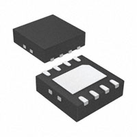
• Packaging:
- 8-Lead, 2 mm x 3 mm DFN
- 5-Lead, SOT-23
The MCP73831/2 devices are highly advanced linear
charge management controllers for use in spacelimited, cost-sensitive applications. The MCP73831/2
are available in an 8-Lead, 2 mm x 3 mm DFN package
or a 5-Lead, SOT-23 package. Along with their small
physical size, the low number of external components
required make the MCP73831/2 ideally suited for
portable applications. For applications charging from a
USB port, the MCP73831/2 adhere to all the
specifications governing the USB power bus.
Applications
•
•
•
•
•
•
•
Lithium-Ion/Lithium-Polymer Battery Chargers
Personal Data Assistants
Cellular Telephones
Digital Cameras
MP3 Players
Bluetooth Headsets
USB Chargers
Typical Application
4.7 F
4 V
DD
470
1
STAT
+ Single
Li-Ion
- Cell
5
VSS 2
The MCP73831/2 devices are fully specified over the
ambient temperature range of -40°C to +85°C.
Package Types
VDD 1
VBAT 3
4.7 F
PROG
Several options are available for the preconditioning
threshold, preconditioning current value, charge
termination value and automatic recharge threshold.
The preconditioning value and charge termination
value are set as a ratio or percentage of the
programmed constant current value. Preconditioning
can be disabled. Refer to Section 1.0 “Electrical
Characteristics” for available options and the
Product Identification System for standard options.
MCP73831/2
2×3 DFN*
500 mA Li-Ion Battery Charger
VIN
The MCP73831/2 employ a constant-current/constantvoltage
charge
algorithm
with
selectable
preconditioning and charge termination. The constant
voltage regulation is fixed with four available options:
4.20V, 4.35V, 4.40V or 4.50V, to accommodate new,
emerging battery charging requirements. The constant
current value is set with one external resistor. The
MCP73831/2 devices limit the charge current based on
die temperature during high power or high ambient
conditions. This thermal regulation optimizes the
charge cycle time while maintaining device reliability.
VDD 2
VBAT 3
VBAT 4
2 k
8 PROG
EP
9
MCP73831/2
SOT-23-5
STAT 1
7 NC
VSS 2
6 VSS
VBAT 3
5 PROG
4 VDD
5 STAT
* Includes Exposed Thermal Pad (EP); see Table 3-1.
MCP73831
2005-2020 Microchip Technology Inc.
DS20001984H-page 1
�MCP73831/2
Functional Block Diagram
VDD
6µA
DIRECTION
CONTROL
VBAT
6µA
G=0.001
NCHRG
0.5µA
PROG
+
REFERENCE
GENERATOR
CA
43.6k
VREF (1.22V)
361k
MCP73831
ONLY
3.9k
+
89k
-
VDD
PRECOND.
182.3k
111k
+
-
15k
STAT
TERM.
+
7k
MPASS
-
CHARGE
+
G=0.001
111k
190k
VA
-
NCHRG
+
-
0.5µA
+
VBAT
-
SHDN
DIRECTION
CONTROL
477k
+
VSS
255k
DS20001984H-page 2
95k
UVLO
-
2005-2020 Microchip Technology Inc.
�MCP73831/2
1.0
ELECTRICAL
CHARACTERISTICS
† Notice: Stresses above those listed under “Maximum
Ratings” may cause permanent damage to the device.
This is a stress rating only and functional operation of
the device at those or any other conditions above those
indicated in the operational listings of this specification
is not implied. Exposure to maximum rating conditions
for extended periods may affect device reliability.
Absolute Maximum Ratings†
VDD...................................................................................7.0V
All Inputs and Outputs w.r.t. VSS ............... -0.3 to (VDD+0.3)V
Maximum Junction Temperature, TJ ............ Internally Limited
Storage temperature .....................................-65°C to +150°C
ESD protection on all pins:
Human Body Model (1.5 k in Series with 100 pF)4 kV
Machine Model (200 pF, No Series Resistance) .............400V
DC CHARACTERISTICS
Electrical Specifications: Unless otherwise indicated, all limits apply for VDD= [VREG(typical) + 1.0V] to 6V, TA = -40°C to +85°C.
Typical values are at +25°C.
Parameters
Sym.
Min.
Typ.
Max.
Units
Conditions
Supply Voltage
VDD
3.75
—
6
V
Supply Current
ISS
—
510
1500
µA
Charging
—
53
200
µA
Charge Complete,
No Battery
—
25
50
µA
PROG Floating
—
1
5
µA
VDD < (VBAT - 50 mV)
—
0.1
2
µA
VDD < VSTOP
Supply Input
UVLO Start Threshold
VSTART
3.3
3.45
3.6
V
VDD Low-to-High
UVLO Stop Threshold
VSTOP
3.2
3.38
3.5
V
VDD High-to-Low
UVLO Hysteresis
VHYS
—
70
—
mV
4.168
4.20
4.232
V
MCP7383X-2
4.317
4.35
4.383
V
MCP7383X-3
4.367
4.40
4.433
V
MCP7383X-4
4.466
4.50
4.534
V
MCP7383X-5
Voltage Regulation (Constant-Voltage Mode)
Regulated Output Voltage
VREG
VDD = [VREG(typical)+1V]
IOUT = 10 mA
TA = -5°C to +55°C
Line Regulation
VBAT/
VBAT)/VDD|
—
0.09
0.30
%/V
Load Regulation
VBAT/VBAT|
—
0.05
0.30
%
IOUT = 10 mA to 50 mA
VDD = [VREG(typical)+1V]
PSRR
—
52
—-
dB
IOUT=10 mA, 10Hz to 1 kHz
—
47
—
dB
IOUT=10 mA, 10Hz to 10 kHz
—
22
—
dB
IOUT=10 mA, 10Hz to 1 MHz
Supply Ripple Attenuation
VDD = [VREG(typical)+1V] to
6V, IOUT = 10 mA
Current Regulation (Fast Charge Constant-Current Mode)
Fast Charge Current
Regulation
IREG
90
100
110
mA
PROG = 10 k
450
505
550
mA
PROG = 2.0 kNote 1
12.5
14.5
16.5
mA
PROG = 67 k
TA = -5°C to +55°C
Note 1:
Not production tested. Ensured by design.
2005-2020 Microchip Technology Inc.
DS20001984H-page 3
�MCP73831/2
DC CHARACTERISTICS (CONTINUED)
Electrical Specifications: Unless otherwise indicated, all limits apply for VDD= [VREG(typical) + 1.0V] to 6V, TA = -40°C to +85°C.
Typical values are at +25°C.
Parameters
Sym.
Min.
Typ.
Max.
Units
Conditions
Preconditioning Current Regulation (Trickle Charge Constant-Current Mode)
Precondition Current
Ratio
IPREG / IREG
7.5
10
12.5
%
PROG = 2.0 kto 10 k
15
20
25
%
PROG = 2.0 kto 10 k
30
40
50
%
PROG = 2.0 kto 10 k
—
100
—
%
No Preconditioning
TA = -5°C to +55°C
Precondition Voltage
Threshold Ratio
Precondition Hysteresis
VPTH / VREG
64
66.5
69
%
VBAT Low-to-High
69
71.5
74
%
VBAT Low-to-High
VPHYS
—
110
—
mV
VBAT High-to-Low
ITERM / IREG
3.75
5
6.25
%
5.6
7.5
9.4
%
PROG = 2.0 kto 10 k
8.5
10
11.5
%
PROG = 2.0 kto 10 k
15
20
25
%
PROG = 2.0 kto 10 k
Charge Termination
Charge Termination
Current Ratio
PROG = 2.0 kto 10 k
TA = -5°C to +55°C
Automatic Recharge
91.5
94.0
96.5
%
VBAT High-to-Low
94
96.5
99
%
VBAT High-to-Low
RDSON
—
350
—
m
VDD = 3.75V, TJ = 105°C
Battery Detection Current
IBAT_DET
0.6
6
—
µA
VBAT Source Current
No-Battery-Present
Threshold
VNO_BAT
—
VREG +
100 mV
—
V
VBAT Voltage ≥ VNO_BAT for
No Battery condition
No-Battery-Present
Impedance
ZNO_BAT
7
—
—
M
VBAT Impedance ≥ ZNO_BAT
for No Battery condition,
Note 1
IDISCHARGE
—
0.15
2
µA
PROG Floating
—
0.25
2
µA
VDD Floating
—
0.15
2
µA
VDD < VSTOP
—
-5.5
-15
µA
Charge Complete
Recharge Voltage
Threshold Ratio
VRTH / VREG
Pass Transistor ON-Resistance
ON-Resistance
Battery Detection
Battery Discharge Current
Output Reverse Leakage
Current
Status Indicator – STAT
Sink Current
ISINK
—
—
25
mA
Low Output Voltage
VOL
—
0.4
1
V
ISOURCE
—
—
35
mA
VOH
—
VDD-0.4
VDD - 1
V
ISOURCE = 4 mA (MCP73831)
ILK
—
0.03
1
µA
High-Impedance
Charge Impedance
Range
RPROG
2
—
67
k
Minimum Shutdown
Impedance
RPROG
70
—
200
k
VPDENTER
VDD VPTH
VBAT < VRTH
VBAT = VREG
CONSTANT VOLTAGE
MODE
Charge Voltage = VREG
STAT = LOW
IBAT < ITERM
CHARGE COMPLETE
MODE
No Charge Current
STAT = HIGH (MCP73831)
STAT = High Z (MCP73832)
FIGURE 4-1:
4.1
Flowchart.
Undervoltage Lockout (UVLO)
An internal UVLO circuit monitors the input voltage and
keeps the charger in Shutdown mode until the input
supply rises above the UVLO threshold. The UVLO
circuitry has a built in hysteresis of 100 mV.
In the event a battery is present when the input power
is applied, the input supply must rise to a level 150 mV
above the battery voltage before the MCP73831/2
become operational.
2005-2020 Microchip Technology Inc.
The UVLO circuit places the device in Shutdown mode
if the input supply falls to within +50 mV of the battery
voltage. Again, the input supply must rise to a level
150 mV above the battery voltage before the
MCP73831/2 become operational.
4.2
Battery Detection
A 6 µA (typical) current is sourced by the VBAT pin to
determine if a battery is present or not. If the voltage at
VBAT rises to VREG + 100 mV (typical), the device
assumes that a battery is not present. If the voltage
stays below VREG + 100 mV (typical), the device
assumes that a battery is detected. In order to correctly
detect a battery insertion, the impedance seen by the
VBAT pin before the battery is connected must be
greater than 7 MΩ due to the minimum battery
detection current of 0.6 µA
4.3
Charge Qualification
For a charge cycle to begin, all UVLO conditions must
be met and a battery or output load must be present. A
charge current programming resistor must be
connected from PROG to VSS. If the PROG pin is open
or floating, the MCP73831/2 are disabled and the
battery reverse discharge current is less than 2 µA. In
this manner, the PROG pin acts as a charge enable
and can be used as a manual shutdown.
4.4
Preconditioning
If the voltage at the VBAT pin is less than the
preconditioning threshold, the MCP73831/2 enter a
preconditioning or Trickle Charge mode. The
preconditioning threshold is factory set. Refer to
Section 1.0
“Electrical
Characteristics”
for
preconditioning threshold options and the Product
Identification System for standard options.
In this mode, the MCP73831/2 supply a percentage of
the charge current (established with the value of the
resistor connected to the PROG pin) to the battery. The
percentage or ratio of the current is factory set. Refer to
Section 1.0
“Electrical
Characteristics”
for
preconditioning current options and the Product Identification System for standard options.
When the voltage at the VBAT pin rises above the
preconditioning threshold, the MCP73831/2 enter the
Constant-Current or Fast Charge mode.
DS20001984H-page 13
�MCP73831/2
300
225
150
75
155
145
135
125
115
95
105
85
0
Charge Termination
The charge cycle is terminated when, during ConstantVoltage mode, the average charge current diminishes
below a percentage of the programmed charge current
(established with the value of the resistor connected to
the PROG pin). A 1 ms filter time on the termination
comparator ensures that transient load conditions do
not result in premature charge cycle termination. The
percentage or ratio of the current is factory set. Refer to
Section 1.0 “Electrical Characteristics” for charge
termination current options and the Product
Identification System for standard options.
375
75
4.7
RPROG = 2 k
450
65
When the voltage at the VBAT pin reaches the
regulation voltage, VREG, constant voltage regulation
begins. The regulation voltage is factory set to 4.2V,
4.35V, 4.40V or 4.50V with a tolerance of ±0.75%.
525
55
Constant-Voltage Mode
The MCP73831/2 limit the charge current based on the
die temperature. The thermal regulation optimizes the
charge cycle time while maintaining device reliability.
Figure 4-2 depicts the thermal regulation for the
MCP73831/2.
25
4.6
Thermal Regulation
45
During the Constant-Current mode, the programmed
charge current is supplied to the battery or load. The
charge current is established using a single resistor
from PROG to VSS. Constant-Current mode is
maintained until the voltage at the VBAT pin reaches the
regulation voltage, VREG.
4.9
35
Fast Charge Constant-Current
Mode
Charge Current (mA)
4.5
Junction Temperature (°C)
FIGURE 4-2:
4.10
Thermal Regulation.
Thermal Shutdown
The MCP73831/2 suspend charge if the die
temperature exceeds 150°C. Charging will resume
when the die temperature has cooled by approximately
10°C.
The charge current is latched off and the MCP73831/2
enter a Charge Complete mode.
4.8
Automatic Recharge
The MCP73831/2 continuously monitor the voltage at
the VBAT pin in the Charge Complete mode. If the
voltage drops below the recharge threshold, another
charge cycle begins and current is once again supplied
to the battery or load. The recharge threshold is factory
set. Refer to Section 1.0 “Electrical Characteristics”
for recharge threshold options and the Product
Identification System for standard options.
DS20001984H-page 14
2005-2020 Microchip Technology Inc.
�MCP73831/2
5.0
DETAILED DESCRIPTION
5.2
5.1
Analog Circuitry
5.2.1
5.1.1
BATTERY MANAGEMENT INPUT
SUPPLY (VDD)
The VDD pin is the input supply pin for the MCP73831/
2 devices. The MCP73831/2 automatically enter a
Power-Down mode if the voltage on the VDD input falls
below the UVLO voltage (VSTOP). This feature prevents
draining the battery pack when the VDD supply is not
present.
5.1.2
CURRENT REGULATION SET
(PROG)
Fast charge current regulation can be scaled by placing
a programming resistor (RPROG) from the PROG input
to VSS. The program resistor and the charge current
are calculated using the following equation:
I REG
1000V
= ----------------RPROG
Where:
RPROG
=
kOhms
IREG
=
milliampere
The preconditioning trickle charge current and the
charge termination current are ratiometric to the fast
charge current based on the selected device options.
5.1.3
BATTERY CHARGE CONTROL
OUTPUT (VBAT)
The battery charge control output is the drain terminal
of an internal P-channel MOSFET. The MCP73831/2
provide constant current and voltage regulation to the
battery pack by controlling this MOSFET in the linear
region. The battery charge control output should be
connected to the positive terminal of the battery pack.
2005-2020 Microchip Technology Inc.
Digital Circuitry
STATUS INDICATOR (STAT)
The charge status output of the MCP73831 has three
different states: High (H), Low (L), and HighImpedance (High Z). The charge status output of the
MCP73832 is open-drain. It has two different states:
Low (L) and High-Impedance (High Z). The charge status output can be used to illuminate one, two or tri-color
LEDs. Optionally, the charge status output can be used
as an interface to a host microcontroller.
Table 5-1 summarizes the state of the status output
during a charge cycle.
TABLE 5-1:
STATUS OUTPUT
Charge Cycle State
STAT1
MCP73831 MCP73832
Shutdown
High Z
High Z
No Battery Present
High Z
High Z
Preconditioning
L
L
Constant-Current Fast
Charge
L
L
Constant Voltage
L
L
Charge Complete –
Standby
H
High Z
5.2.2
DEVICE DISABLE (PROG)
The current regulation set input pin (PROG) can be
used to terminate a charge at any time during the
charge cycle, as well as to initiate a charge cycle or
initiate a recharge cycle.
Placing a programming resistor from the PROG input to
VSS enables the device. Allowing the PROG input to
float or by applying a logic-high input signal, disables
the device and terminates a charge cycle. When
disabled, the device’s supply current is reduced to
25 µA, typically.
DS20001984H-page 15
�MCP73831/2
NOTES:
DS20001984H-page 16
2005-2020 Microchip Technology Inc.
�MCP73831/2
6.0
APPLICATIONS
followed by a constant voltage charging method.
Figure 6-1 depicts a typical stand-alone application
circuit, while Figure 6-2 and Figure 6-3 depict the
accompanying charge profile.
The MCP73831/2 are designed to operate in
conjunction with a host microcontroller or in a standalone application. The MCP73831/2 provide the
preferred charge algorithm for Lithium-Ion and LithiumPolymer cells. The algorithm uses a constant current
Li-Ion Battery Charger
4
RLED
CIN
PROG
SMAJ5.0A/AC
REGULATED
WALL CUBE
VBAT
VDD
3
COUT
5
RPROG
LED
1
VSS
STAT
+ Single
Li-Ion
- Cell
2
SOT-23-5
MCP73831/2
120
6.0
600
5.0
100
5.0
500
4.0
80
4.0
400
3.0
60
3.0
300
2.0
40
Time (minutes)
FIGURE 6-2:
Typical Charge Profile
(180 mAh Battery).
6.1
240
210
180
150
120
90
0
Time (minutes)
FIGURE 6-3:
Typical Charge Profile in
Thermal Regulation (1000 mAh Battery).
Application Circuit Design
Due to the low efficiency of linear charging, the most
important factors are thermal design and cost, which
are a direct function of the input voltage, output current
and thermal impedance between the battery charger
and the ambient cooling air. The worst-case situation is
when the device has transitioned from the
Preconditioning mode to the Constant-Current mode.
In this situation, the battery charger has to dissipate the
maximum power. A trade-off must be made between
the charge current, cost and thermal requirements of
the charger.
6.1.1
100
0.0
180
160
140
120
100
80
60
40
20
0
0
0.0
1.0
60
20
200
MCP73831-2AC/IOT
VDD = 5.2V
RPROG = 2 kΩ
30
1.0
2.0
0
MCP73831-2AC/IOT
VDD = 5.2V
RPROG = 10 kΩ
Battery Voltage (V)
6.0
Charge Current (mA)
Typical Application Circuit.
Charge Current (mA)
Battery Voltage (V)
FIGURE 6-1:
6.1.1.1
Current Programming Resistor
(RPROG)
The preferred fast charge current for Lithium-Ion cells
is at the 1C rate, with an absolute maximum current at
the 2C rate. For example, a 500 mAh battery pack has
a preferred fast charge current of 500 mA. Charging at
this rate provides the shortest charge cycle times
without degradation to the battery pack performance or
life.
COMPONENT SELECTION
Selection of the external components in Figure 6-1 is
crucial to the integrity and reliability of the charging
system. The following discussion is intended as a guide
for the component selection process.
2005-2020 Microchip Technology Inc.
DS20001984H-page 17
�MCP73831/2
6.1.1.2
Input Overvoltage Protection (IOVP)
Input overvoltage protection must be used when the
input power source is hot-pluggable. This includes USB
cables and Wall-type power supplies. The cabling of
these supplies acts as an inductor. When the supplies
are connected/disconnected from the system, large
voltage transients are created which may damage the
system circuitry. These transients should be snubbed
out. A transzorb connected from the V+ input supply
connector to the 0V ground reference will snub the
transients.
6.1.1.3
Thermal Considerations
The worst-case power dissipation in the battery
charger occurs when the input voltage is at the
maximum and the device has transitioned from the
Preconditioning mode to the Constant-Current mode.
In this case, the power dissipation is:
PowerDissipation = V DDMAX – VPTHMIN I REGMAX
Where:
VDDMAX
=
the maximum input voltage
IREGMAX
=
the maximum fast charge current
VPTHMIN
=
the minimum transition threshold
voltage
Power dissipation with a 5V, ±10% input voltage source
is:
PowerDissipation = 5.5V – 2.7V 550mA = 1.54W
This power dissipation with the battery charger in the
SOT-23-5 package will cause thermal regulation to be
entered as depicted in Figure 6-3. Alternatively, the
2mm x 3mm DFN package could be utilized to reduce
charge cycle times.
6.1.1.4
External Capacitors
The MCP73831/2 are stable with or without a battery
load. In order to maintain good AC stability in the
Constant-Voltage mode, a minimum capacitance of
4.7 µF is recommended to bypass the VBAT pin to VSS.
This capacitance provides compensation when there is
no battery load. In addition, the battery and
interconnections appear inductive at high frequencies.
These elements are in the control feedback loop during
Constant-Voltage mode. Therefore, the bypass
capacitance may be necessary to compensate for the
inductive nature of the battery pack.
Virtually any good quality output filter capacitor can be
used, independent of the capacitor’s minimum
Effective Series Resistance (ESR) value. The actual
value of the capacitor (and its associated ESR)
depends on the output load current. A 4.7 µF ceramic,
tantalum or aluminum electrolytic capacitor at the
output is usually sufficient to ensure stability for output
currents up to a 500 mA.
DS20001984H-page 18
6.1.1.5
Reverse-Blocking Protection
The MCP73831/2 provide protection from a faulted or
shorted input. Without the protection, a faulted or
shorted input would discharge the battery pack through
the body diode of the internal pass transistor.
6.1.1.6
Charge Inhibit
The current regulation set input pin (PROG) can be
used to terminate a charge at any time during the
charge cycle, as well as to initiate a charge cycle or
initiate a recharge cycle.
Placing a programming resistor from the PROG input to
VSS enables the device. Allowing the PROG input to
float or by applying a logic-high input signal, disables
the device and terminates a charge cycle. When
disabled, the device’s supply current is reduced to
25 µA, typically.
6.1.1.7
Charge Status Interface
A status output provides information on the state of
charge. The output can be used to illuminate external
LEDs or interface to a host microcontroller. Refer to
Table 5-1 for a summary of the state of the status
output during a charge cycle.
6.2
PCB Layout Issues
For optimum voltage regulation, place the battery pack
as close as possible to the device’s VBAT and VSS pins.
This is recommended to minimize voltage drops along
the high current-carrying PCB traces.
If the PCB layout is used as a heat sink, adding many
vias in the heat sink pad can help conduct more heat to
the PCB backplane, thus reducing the maximum
junction temperature. Figure 6-4 and Figure 6-5 depict
a typical layout with PCB heatsinking.
RLED LED
VSS
VBAT
FIGURE 6-4:
RPROG
COUT MCP73831 C
IN
VDD
Typical Layout (Top).
VSS
VBAT
FIGURE 6-5:
VDD
Typical Layout (Bottom).
2005-2020 Microchip Technology Inc.
�MCP73831/2
7.0
PACKAGING INFORMATION
7.1
Package Marking Information
8-Lead DFN (2x3x0.9 mm)
Device
Code
MCP73831T-2ACI/MC
AAE
MCP73831T-2ATI/MC
AAF
MCP73831T-2DCI/MC
AAG
MCP73831T-3ACI/MC
AAH
MCP73831T-4ADI/MC
AAJ
MCP73831T-5ACI/MC
AAK
MCP73832T-2ACI/MC
AAL
MCP73832T-2ATI/MC
AAM
MCP73832T-2DCI/MC
AAP
MCP73832T-3ACI/MC
AAQ
MCP73832T-4ADI/MC
AAR
MCP73832T-5ACI/MC
AAS
Example
AAE
739
25
Note: Applies to 8-Lead DFN
5-Lead SOT-23
XXNN
Device
Example
Code
MCP73831T-2ACI/OT
KDNN
MCP73831T-2ATI/OT
KENN
MCP73831T-2DCI/OT
KFNN
MCP73831T-3ACI/OT
KGNN
MCP73831T-4ADI/OT
KHNN
MCP73831T-5ACI/OT
KJNN
MCP73832T-2ACI/OT
KKNN
MCP73832T-2ATI/OT
KLNN
MCP73832T-2DCI/OT
KMNN
MCP73832T-3ACI/OT
KPNN
MCP73832T-4ADI/OT
KQNN
MCP73832T-5ACI/OT
KRNN
MCP73832T-2DFI/OT
LUNN
KD25
Note: Applies to 5-Lead SOT-23
Legend: XX...X
Y
YY
WW
NNN
e3
*
Note:
Customer-specific information
Year code (last digit of calendar year)
Year code (last 2 digits of calendar year)
Week code (week of January 1 is week ‘01’)
Alphanumeric traceability code
Pb-free Compliant JEDEC® designator for Matte Tin (Sn)
This package is Pb-free. The Pb-free JEDEC designator ( e3 )
can be found on the outer packaging for this package.
In the event the full Microchip part number cannot be marked on one line, it will be carried over
to the next line, thus limiting the number of available characters for customer-specific
information.
2005-2020 Microchip Technology Inc.
DS20001984H-page 19
�MCP73831/2
��/HDG�3ODVWLF�'XDO�)ODW��1R�/HDG�3DFNDJH��0&��±��[�[����PP�%RG\�>')1@
1RWH�
4���%�
�&� %��!��
�%�
��*��
�"��)��� '�
�
�
�
�%�
���������
����*�������
��$���%��������%
"��%�
�%%
255)))�&�������
���&5
��*�����
e
D
b
N
N
L
K
E2
E
EXPOSED PAD
NOTE 1
NOTE 1
2
1
2
1
D2
BOTTOM VIEW
TOP VIEW
A
A3
A1
NOTE 2
6��%
��&
� ����9�&�%
:!&(
���$����
��99��,�,��
��:
:
:;�
��<
=
��%��
;�
�����>
���%
�
��=�
����
����
�%��"�$$�
��
����
����
���.
0��%��%�����*�
�+
������,4
;�
�����9
��%�
�
�����/�0
;�
�����?�"%�
,
,#
�
"���"�9
��%�
��
��+�
@
,#
�
"���"�?�"%�
,�
��.�
@
���.
(
����
���.
��+�
0��%��%�9
��%�
9
��+�
����
��.�
0��%��% %� ,#
�
"���"
F
����
@
@
0��%��%�?�"%�
��.��/�0
+����/�0
1RWHV�
�� �������� !�����"
#�$
�%!�
�&�������'�(!%�&! %�(
�����%
"�)�%����%�
���%��
"���
��
�� ���*��
�&������
���
����&��
�
#
�
"�%�
�(�� ��%�
�" �
+� ���*��
�� � �)� ���!��%
"�
�� ��&
� ���������"�%��
��������
�����,�-���.��
/�02 /� �����&
� �������
��
%�������
#��%����!
� ��)��)�%��!%�%��
����
�
�,42 �
$
�
��
���&
� ���'�! !�����)�%��!%�%��
����
'�$�����$��&�%����
!�
�
������
��..
��������
�
�������� ���)��� 0�� ��+0
DS20001984H-page 20
2005-2020 Microchip Technology Inc.
�MCP73831/2
Note:
For the most current package drawings, please see the Microchip Packaging Specification located at
http://www.microchip.com/packaging
2005-2020 Microchip Technology Inc.
DS20001984H-page 21
�MCP73831/2
5-Lead Plastic Small Outline Transistor (OT) [SOT23]
Note:
For the most current package drawings, please see the Microchip Packaging Specification located at
http://www.microchip.com/packaging
0.20 C 2X
D
e1
A
D
N
E/2
E1/2
E1
E
(DATUM D)
(DATUM A-B)
0.15 C D
2X
NOTE 1
1
2
e
B
NX b
0.20
C A-B D
TOP VIEW
A
A A2
0.20 C
SEATING PLANE
A
SEE SHEET 2
A1
C
SIDE VIEW
Microchip Technology Drawing C04-091-OT Rev F Sheet 1 of 2
DS20001984H-page 22
2005-2020 Microchip Technology Inc.
�MCP73831/2
5-Lead Plastic Small Outline Transistor (OT) [SOT23]
Note:
For the most current package drawings, please see the Microchip Packaging Specification located at
http://www.microchip.com/packaging
c
T
L
L1
VIEW A-A
SHEET 1
Units
Dimension Limits
N
Number of Pins
e
Pitch
e1
Outside lead pitch
A
Overall Height
A2
Molded Package Thickness
Standoff
A1
Overall Width
E
Molded Package Width
E1
Overall Length
D
Foot Length
L
Footprint
L1
I
Foot Angle
c
Lead Thickness
b
Lead Width
MIN
0.90
0.89
-
0.30
0°
0.08
0.20
MILLIMETERS
NOM
5
0.95 BSC
1.90 BSC
2.80 BSC
1.60 BSC
2.90 BSC
0.60 REF
-
MAX
1.45
1.30
0.15
0.60
10°
0.26
0.51
Notes:
1. Dimensions D and E1 do not include mold flash or protrusions. Mold flash or
protrusions shall not exceed 0.25mm per side.
2. Dimensioning and tolerancing per ASME Y14.5M
BSC: Basic Dimension. Theoretically exact value shown without tolerances.
REF: Reference Dimension, usually without tolerance, for information purposes only.
Microchip Technology Drawing C04-091-OT Rev F Sheet 2 of 2
2005-2020 Microchip Technology Inc.
DS20001984H-page 23
�MCP73831/2
5-Lead Plastic Small Outline Transistor (OT) [SOT23]
Note:
For the most current package drawings, please see the Microchip Packaging Specification located at
http://www.microchip.com/packaging
X
SILK SCREEN
5
Y
Z
C
G
1
2
E
GX
RECOMMENDED LAND PATTERN
Units
Dimension Limits
E
Contact Pitch
C
Contact Pad Spacing
X
Contact Pad Width (X5)
Contact Pad Length (X5)
Y
Distance Between Pads
G
Distance Between Pads
GX
Overall Width
Z
MIN
MILLIMETERS
NOM
0.95 BSC
2.80
MAX
0.60
1.10
1.70
0.35
3.90
Notes:
1. Dimensioning and tolerancing per ASME Y14.5M
BSC: Basic Dimension. Theoretically exact value shown without tolerances.
Microchip Technology Drawing No. C04-2091-OT Rev F
DS20001984H-page 24
2005-2020 Microchip Technology Inc.
�MCP73831/2
APPENDIX A:
REVISION HISTORY
Revision H (June 2020)
Revision D (April 2008)
The following is the list of modifications:
1.
The following is the list of modifications:
1.
2.
3.
4.
5.
6.
Updated the Functional Block Diagram.
Updated the DC Characteristics table.
Updated the AC Characteristics table.
Updated the
Temperature Specifications
table.
Updated Section 4.2, Battery Detection.
Updated Figure 6-1.
Changed Charge Termination Current Ratio to
8.5% minimum and 11.5% maximum.
Revision C (October 2007)
The following is the list of modifications:
1.
2.
3.
Numerous edits throughout document.
Added note to the Temperature Specifications
table.
Updated Figure 2-4.
Revision G (July 2014)
Revision B (March 2006)
The following is the list of modifications:
The following is the list of modifications:
7.
8.
1.
Updated the DC Characteristics table.
Added Section 6.1.1.2, Input Overvoltage
Protection (IOVP).
Revision F (June 2013)
Added MCP73832 through document.
Revision A (November 2005)
Original release of this document.
The following is the list of modifications:
9. Updated the Functional Block Diagram.
10. Added the Battery Detection parameter and
related information in the DC Characteristics
table.
11. Added new section Section 4.2, Battery Detection.
12. Minor grammatical and spelling corrections.
Revision E (September 2008)
The following is the list of modifications:
1.
2.
3.
4.
5.
6.
7.
Package Types: Changed DFN pinout diagram.
Section 1.0,
Electrical
Characteristics:
Changed “Charge Impedance Range from
20 k to 67 k
Section 1.0, Electrical Characteristics: Misc.
Formatting changes.
Section 2.0, Typical Performance Curves:
Updated Figure 2-4.
Section 3.0, Pin Description: Added Exposed
Pad pin to table and added Section 3.6,
Exposed Thermal Pad (EP).
Updated Appendix A: Revision History
Added Land Pattern Package Outline Drawing
for 2x3 DFN package.
2005-2020 Microchip Technology Inc.
DS20001984H-page 25
�MCP73831/2
PRODUCT IDENTIFICATION SYSTEM
To order or obtain information, e.g., on pricing or delivery, refer to the factory or the listed sales office.
PART NO.
X
XX
Examples: *
/XX
X
a)
Device
VREG
Options Temperature Package
Range
b)
c)
Device:
MCP73831:
MCP73831T:
Single-Cell Charge Controller
Single-Cell Charge Controller
(Tape and Reel)
Single-Cell Charge Controller
Single-Cell Charge Controller
(Tape and Reel)
MCP73832
MCP73832T:
Regulation
Voltage:
Code
VREG
2
3
4
5
4.20V
4.35V
4.40V
4.50V
=
=
=
=
d)
a)
b)
c)
d)
a)
b)
Options: *
Code
AC
AD
AT
DC
IPREG/IREG
VPTH/VREG
ITERM/IREG
VRTH/VREG
10
10
10
100
66.5
66.5
71.5
x
7.5
7.5
20
7.5
96.5
94
94
96.5
* Consult Factory for Alternative Device Options
c)
d)
a)
b)
Temperature
Range:
I
Package:
MC
OT
= -40C to +85C (Industrial)
c)
= Dual-Flat, No-Lead (2x3 mm body), 8-Lead
= Small Outline Transistor (SOT23), 5-Lead
d)
a)
b)
c)
d)
a)
b)
c)
d)
MCP73831-2ACI/OT: 4.20V VREG,
Options AC, 5LD SOT23 package
MCP73831T-2ACI/OT: Tape and Reel,
4.20V VREG, Options AC, 5LD SOT23 package
MCP73832-2ACI/MC: 4.20V VREG,
Options AC, 8LD DFN package
MCP73832T-2ACI/MC: Tape and Reel,
4.20V VREG, Options AC, 8LD DFN package
MCP73831-2ATI/OT: 4.20V VREG,
Options AT, 5LD SOT23 package
MCP73831T-2ATI/OT: Tape and Reel,
4.20V VREG, Options AT, 5LD SOT23 package
MCP73832-2ATI/MC: 4.20V VREG,
Options AT, 8LD DFN package
MCP73832T-2ATI/MC: Tape and Reel,
4.20V VREG, Options AT, 8LD DFN package
MCP73831-2DCI/OT: 4.20V VREG,
Options DC, 5LD SOT23 package
MCP73831T-2DCI/OT: Tape and Reel,
4.20V VREG, Options DC, 5LD SOT23 package
MCP73832-2DCI/MC: 4.20V VREG,
Options DC, 8LD DFN package
MCP73832T-2DCI/MC: Tape and Reel,
4.20V VREG, Options DC, 8LD DFN package
MCP73831-3ACI/OT: 4.35V VREG,
Options AC, 5LD SOT23 package
MCP73831T-3ACI/OT: Tape and Reel,
4.35V VREG, Options AC, 5LD SOT23 package
MCP73832-3ACI/MC: 4.35V VREG,
Options AC, 8LD DFN package
MCP73832T-3ACI/MC: Tape and Reel,
4.35V VREG, Options AC, 8LD DFN package
MCP73831-4ADI/OT: 4.40V VREG,
Options AD, 5LD SOT23 package
MCP73831T-4ADI/OT: Tape and Reel,
4.40V VREG, Options AD, 5LD SOT23 package
MCP73832-4ADI/MC: 4.40V VREG,
Options AD, 8LD DFN package
MCP73832T-4ADI/MC: Tape and Reel,
4.40V VREG, Options AD, 8LD DFN package
MCP73831-5ACI/OT: 4.50V VREG,
Options AC, 5LD SOT23 package
MCP73831T-5ACI/OT: Tape and Reel,
4.50V VREG, Options AC, 5LD SOT23 package
MCP73832-5ACI/MC: 4.50V VREG,
Options AC, 8LD DFN package
MCP73832T-5ACI/MC: Tape and Reel,
4.50V VREG, Options AC, 8LD DFN package
* Consult Factory for Alternate Device Options
2005-2020 Microchip Technology Inc.
DS20001984H-page 26
�MCP73831/2
NOTES:
DS20001984H-page 27
2005-2020 Microchip Technology Inc.
�Note the following details of the code protection feature on Microchip devices:
•
Microchip products meet the specification contained in their particular Microchip Data Sheet.
•
Microchip believes that its family of products is one of the most secure families of its kind on the market today, when used in the
intended manner and under normal conditions.
•
There are dishonest and possibly illegal methods used to breach the code protection feature. All of these methods, to our
knowledge, require using the Microchip products in a manner outside the operating specifications contained in Microchip’s Data
Sheets. Most likely, the person doing so is engaged in theft of intellectual property.
•
Microchip is willing to work with the customer who is concerned about the integrity of their code.
•
Neither Microchip nor any other semiconductor manufacturer can guarantee the security of their code. Code protection does not
mean that we are guaranteeing the product as “unbreakable.”
Code protection is constantly evolving. We at Microchip are committed to continuously improving the code protection features of our
products. Attempts to break Microchip’s code protection feature may be a violation of the Digital Millennium Copyright Act. If such acts
allow unauthorized access to your software or other copyrighted work, you may have a right to sue for relief under that Act.
Information contained in this publication regarding device
applications and the like is provided only for your convenience
and may be superseded by updates. It is your responsibility to
ensure that your application meets with your specifications.
MICROCHIP MAKES NO REPRESENTATIONS OR
WARRANTIES OF ANY KIND WHETHER EXPRESS OR
IMPLIED, WRITTEN OR ORAL, STATUTORY OR
OTHERWISE, RELATED TO THE INFORMATION,
INCLUDING BUT NOT LIMITED TO ITS CONDITION,
QUALITY, PERFORMANCE, MERCHANTABILITY OR
FITNESS FOR PURPOSE. Microchip disclaims all liability
arising from this information and its use. Use of Microchip
devices in life support and/or safety applications is entirely at
the buyer’s risk, and the buyer agrees to defend, indemnify and
hold harmless Microchip from any and all damages, claims,
suits, or expenses resulting from such use. No licenses are
conveyed, implicitly or otherwise, under any Microchip
intellectual property rights unless otherwise stated.
Trademarks
The Microchip name and logo, the Microchip logo, Adaptec,
AnyRate, AVR, AVR logo, AVR Freaks, BesTime, BitCloud, chipKIT,
chipKIT logo, CryptoMemory, CryptoRF, dsPIC, FlashFlex,
flexPWR, HELDO, IGLOO, JukeBlox, KeeLoq, Kleer, LANCheck,
LinkMD, maXStylus, maXTouch, MediaLB, megaAVR, Microsemi,
Microsemi logo, MOST, MOST logo, MPLAB, OptoLyzer,
PackeTime, PIC, picoPower, PICSTART, PIC32 logo, PolarFire,
Prochip Designer, QTouch, SAM-BA, SenGenuity, SpyNIC, SST,
SST Logo, SuperFlash, Symmetricom, SyncServer, Tachyon,
TempTrackr, TimeSource, tinyAVR, UNI/O, Vectron, and XMEGA
are registered trademarks of Microchip Technology Incorporated in
the U.S.A. and other countries.
APT, ClockWorks, The Embedded Control Solutions Company,
EtherSynch, FlashTec, Hyper Speed Control, HyperLight Load,
IntelliMOS, Libero, motorBench, mTouch, Powermite 3, Precision
Edge, ProASIC, ProASIC Plus, ProASIC Plus logo, Quiet-Wire,
SmartFusion, SyncWorld, Temux, TimeCesium, TimeHub,
TimePictra, TimeProvider, Vite, WinPath, and ZL are registered
trademarks of Microchip Technology Incorporated in the U.S.A.
Adjacent Key Suppression, AKS, Analog-for-the-Digital Age, Any
Capacitor, AnyIn, AnyOut, BlueSky, BodyCom, CodeGuard,
CryptoAuthentication, CryptoAutomotive, CryptoCompanion,
CryptoController, dsPICDEM, dsPICDEM.net, Dynamic Average
Matching, DAM, ECAN, EtherGREEN, In-Circuit Serial
Programming, ICSP, INICnet, Inter-Chip Connectivity, JitterBlocker,
KleerNet, KleerNet logo, memBrain, Mindi, MiWi, MPASM, MPF,
MPLAB Certified logo, MPLIB, MPLINK, MultiTRAK, NetDetach,
Omniscient Code Generation, PICDEM, PICDEM.net, PICkit,
PICtail, PowerSmart, PureSilicon, QMatrix, REAL ICE, Ripple
Blocker, SAM-ICE, Serial Quad I/O, SMART-I.S., SQI,
SuperSwitcher, SuperSwitcher II, Total Endurance, TSHARC,
USBCheck, VariSense, ViewSpan, WiperLock, Wireless DNA, and
ZENA are trademarks of Microchip Technology Incorporated in the
U.S.A. and other countries.
SQTP is a service mark of Microchip Technology Incorporated in
the U.S.A.
The Adaptec logo, Frequency on Demand, Silicon Storage
Technology, and Symmcom are registered trademarks of Microchip
Technology Inc. in other countries.
GestIC is a registered trademark of Microchip Technology Germany
II GmbH & Co. KG, a subsidiary of Microchip Technology Inc., in
other countries.
All other trademarks mentioned herein are property of their
respective companies.
© 2005-2020, Microchip Technology Incorporated, All Rights
Reserved.
For information regarding Microchip’s Quality Management Systems,
please visit www.microchip.com/quality.
2005-2020 Microchip Technology Inc.
ISBN: 978-1-5224-6185-2
DS20001984H-page 28
�Worldwide Sales and Service
AMERICAS
ASIA/PACIFIC
ASIA/PACIFIC
EUROPE
Corporate Office
2355 West Chandler Blvd.
Chandler, AZ 85224-6199
Tel: 480-792-7200
Fax: 480-792-7277
Technical Support:
http://www.microchip.com/
support
Web Address:
www.microchip.com
Australia - Sydney
Tel: 61-2-9868-6733
India - Bangalore
Tel: 91-80-3090-4444
China - Beijing
Tel: 86-10-8569-7000
India - New Delhi
Tel: 91-11-4160-8631
Austria - Wels
Tel: 43-7242-2244-39
Fax: 43-7242-2244-393
China - Chengdu
Tel: 86-28-8665-5511
India - Pune
Tel: 91-20-4121-0141
Denmark - Copenhagen
Tel: 45-4485-5910
Fax: 45-4485-2829
China - Chongqing
Tel: 86-23-8980-9588
Japan - Osaka
Tel: 81-6-6152-7160
Finland - Espoo
Tel: 358-9-4520-820
China - Dongguan
Tel: 86-769-8702-9880
Japan - Tokyo
Tel: 81-3-6880- 3770
China - Guangzhou
Tel: 86-20-8755-8029
Korea - Daegu
Tel: 82-53-744-4301
France - Paris
Tel: 33-1-69-53-63-20
Fax: 33-1-69-30-90-79
China - Hangzhou
Tel: 86-571-8792-8115
Korea - Seoul
Tel: 82-2-554-7200
China - Hong Kong SAR
Tel: 852-2943-5100
Malaysia - Kuala Lumpur
Tel: 60-3-7651-7906
China - Nanjing
Tel: 86-25-8473-2460
Malaysia - Penang
Tel: 60-4-227-8870
China - Qingdao
Tel: 86-532-8502-7355
Philippines - Manila
Tel: 63-2-634-9065
China - Shanghai
Tel: 86-21-3326-8000
Singapore
Tel: 65-6334-8870
China - Shenyang
Tel: 86-24-2334-2829
Taiwan - Hsin Chu
Tel: 886-3-577-8366
China - Shenzhen
Tel: 86-755-8864-2200
Taiwan - Kaohsiung
Tel: 886-7-213-7830
China - Suzhou
Tel: 86-186-6233-1526
Taiwan - Taipei
Tel: 886-2-2508-8600
China - Wuhan
Tel: 86-27-5980-5300
Thailand - Bangkok
Tel: 66-2-694-1351
China - Xian
Tel: 86-29-8833-7252
Vietnam - Ho Chi Minh
Tel: 84-28-5448-2100
Atlanta
Duluth, GA
Tel: 678-957-9614
Fax: 678-957-1455
Austin, TX
Tel: 512-257-3370
Boston
Westborough, MA
Tel: 774-760-0087
Fax: 774-760-0088
Chicago
Itasca, IL
Tel: 630-285-0071
Fax: 630-285-0075
Dallas
Addison, TX
Tel: 972-818-7423
Fax: 972-818-2924
Detroit
Novi, MI
Tel: 248-848-4000
Houston, TX
Tel: 281-894-5983
Indianapolis
Noblesville, IN
Tel: 317-773-8323
Fax: 317-773-5453
Tel: 317-536-2380
Los Angeles
Mission Viejo, CA
Tel: 949-462-9523
Fax: 949-462-9608
Tel: 951-273-7800
Raleigh, NC
Tel: 919-844-7510
New York, NY
Tel: 631-435-6000
San Jose, CA
Tel: 408-735-9110
Tel: 408-436-4270
Canada - Toronto
Tel: 905-695-1980
Fax: 905-695-2078
DS20001984H-page 29
China - Xiamen
Tel: 86-592-2388138
China - Zhuhai
Tel: 86-756-3210040
Germany - Garching
Tel: 49-8931-9700
Germany - Haan
Tel: 49-2129-3766400
Germany - Heilbronn
Tel: 49-7131-72400
Germany - Karlsruhe
Tel: 49-721-625370
Germany - Munich
Tel: 49-89-627-144-0
Fax: 49-89-627-144-44
Germany - Rosenheim
Tel: 49-8031-354-560
Israel - Ra’anana
Tel: 972-9-744-7705
Italy - Milan
Tel: 39-0331-742611
Fax: 39-0331-466781
Italy - Padova
Tel: 39-049-7625286
Netherlands - Drunen
Tel: 31-416-690399
Fax: 31-416-690340
Norway - Trondheim
Tel: 47-7288-4388
Poland - Warsaw
Tel: 48-22-3325737
Romania - Bucharest
Tel: 40-21-407-87-50
Spain - Madrid
Tel: 34-91-708-08-90
Fax: 34-91-708-08-91
Sweden - Gothenberg
Tel: 46-31-704-60-40
Sweden - Stockholm
Tel: 46-8-5090-4654
UK - Wokingham
Tel: 44-118-921-5800
Fax: 44-118-921-5820
2005-2020 Microchip Technology Inc.
02/28/20
�