MCP73871
Stand-Alone System Load Sharing and Li-Ion/Li-Polymer Battery Charge
Management Controller
Features
Applications
• Integrated System Load Sharing and Battery
Charge Management
- Simultaneously Power the System and
Charge the Li-Ion Battery
- Voltage Proportional Current Control (VPCC)
ensures system load has priority over Li-Ion
battery charge current
- Low-Loss Power-Path Management with
Ideal Diode Operation
• Complete Linear Charge Management Controller
- Integrated Pass Transistors
- Integrated Current Sense
- Integrated Reverse Discharge Protection
- Selectable Input Power Sources: USB Port or
AC-DC Wall Adapter
• Preset High Accuracy Charge Voltage Options:
- 4.10V, 4.20V, 4.35V or 4.40V
- ±0.5% Regulation Tolerance
• Constant Current/Constant Voltage (CC/CV)
Operation with Thermal Regulation
• Maximum 1.8A Total Input Current Control
• Resistor Programmable Fast Charge Current
Control: 50 mA to 1A
• Resistor Programmable Termination Set Point
• Selectable USB Input Current Control
- Absolute Maximum: 100 mA (L)/500 mA (H)
• Automatic Recharge
• Automatic End-of-Charge Control
• Safety Timer With Timer Enable/Disable Control
• 0.1C Preconditioning for Deeply Depleted Cells
• Battery Cell Temperature Monitor
• Undervoltage Lockout (UVLO)
• Low Battery Status Indicator (LBO)
• Power Good Status Indicator (PG)
• Charge Status and Fault Condition Indicators
• Numerous Selectable Options Available for a
Variety of Applications:
- Refer to Section 1.0 “Electrical
Characteristics” for Selectable Options
- Refer to the Product Identification System
for Standard Options
• Temperature Range: -40°C to +85°C
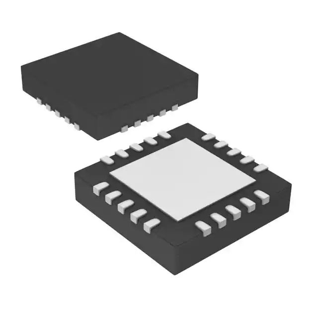
• Packaging: 20-Lead QFN (4 mm x 4 mm)
•
•
•
•
•
•
•
•
2008-2019 Microchip Technology Inc.
GPSs/Navigators
PDAs and Smart Phones
Portable Media Players and MP3 Players
Digital Cameras
Bluetooth® Headsets
Portable Medical Devices
Charge Cradles/Docking Stations
Toys
Description
The MCP73871 device is a fully integrated linear
solution for system load sharing and Li-Ion/Li-Polymer
battery charge management with AC-DC wall adapter
and USB port power sources selection. It is also
capable of autonomous power source selection
between input and battery. Along with its small physical
size, the low number of required external components
makes the device ideally suited for portable
applications.
The MCP73871 device automatically obtains power for
the system load from a single-cell Li-Ion battery or an
input power source (AC-DC wall adapter or USB port).
The MCP73871 device specifically adheres to the
current drawn limits governed by the USB specification.
With an AC-DC wall adapter providing power to the
system, an external resistor sets the magnitude of 1A
maximum charge current while supporting up to 1.8A
total current for system load and battery charge
current.
The MCP73871 device employs a constant
current/constant voltage (CC/CV) charge algorithm
with selectable charge termination point. To
accommodate new and emerging battery charging
requirements, the constant voltage regulation is fixed
with four available options: 4.10V, 4.20V, 4.35V or
4.40V. The MCP73871 device also limits the charge
current based on the die temperature during high
power or high ambient conditions. This thermal
regulation optimizes the charge cycle time while
maintaining device reliability.
The MCP73871 device includes a low battery indicator,
a power good indicator and two charge status
indicators that allow for outputs with LEDs or
communication with host microcontrollers. The
MCP73871 device is fully specified over the ambient
temperature range of -40°C to +85°C.
DS20002090E-page 1
�MCP73871
Package Types
CE
VBAT_SENSE
IN
IN
OUT
MCP73871
20-Lead QFN*
20 19 18 17 16
OUT 1
15
VPCC 2
SEL 3
14 VBAT
EP
21
12
11
8
9 10
TE
VSS
7
PG
STAT2
6
13
STAT1/LBO
PROG2 4
THERM 5
VBAT
PROG1
PROG3
VSS
* Includes Exposed Thermal Pad (EP); see Table 3-1.
Typical Application Circuit
MCP73871 Typical Application
AC-DC Adapter
or
USB Port
18, 19
10 μF
2
470
Low Hi
Low Hi
Low Hi
Low Hi
DS20002090E-page 2
6
IN
1, 20
System
Load
4.7 μF
VPCC
VBAT 14, 15, 16
4.7 μF
PG
470
7 STAT2
470
8 STAT1
LBO
3
SEL
4
OUT
PROG2
THERM 5
NTC
10 k
PROG1 13 RPROG1
Single-Cell
Li-Ion Battery
R
PROG3 12 PROG3
9 TE
17
CE
VSS 10, 11, EP
2008-2019 Microchip Technology Inc.
�MCP73871
Functional Block Diagram
Direction
Control
0.2
IN
G = 0.001
OUT
CURRENT
LIMIT
0.2
VREF
Ideal
Diode,
Synchronous
Switch
+
Direction
Control
VBAT
PROG1
G = 0.001
PROG3
G = 0.001
G = 0.001
CURRENT
LIMIT
+
VREF
-
VPCC
VREF/2
+
-
SEL
PROG2
CA
+
VREF
-
PRECONDITION
+
CHRG
361k VBAT_SENSE
VREF
89k
VREF
+
7k
VA
+
-
VREF
-
VREF
190k
PG
VREF
50 μA
THERM
+
LTVT
-
CE
HTVT
-
TE
TERM
+
STAT2
UVLO,
REFERENCE,
CHARGE
CONTROL,
TIMER,
AND
STATUS
LOGIC
+
STAT1
VSS
VREF (1.21V)
2008-2019 Microchip Technology Inc.
DS20002090E-page 3
�MCP73871
NOTES:
DS20002090E-page 4
2008-2019 Microchip Technology Inc.
�MCP73871
1.0
ELECTRICAL
CHARACTERISTICS
† Notice: Stresses above those listed under “Maximum
Ratings” may cause permanent damage to the device.
This is a stress rating only and functional operation of
the device at those or any other conditions above those
indicated in the operational listings of this specification
is not implied. Exposure to maximum rating conditions
for extended periods may affect device reliability.
Absolute Maximum Ratings†
VIN ....................................................................................7.0V
All Inputs and Outputs w.r.t.VSS ................ -0.3V to VDD+0.3V
(VDD = VIN or VBAT)
Maximum Junction Temperature, TJ ............ Internally Limited
Storage temperature .....................................-65°C to +150°C
ESD protection on all pins
Human Body Model (1.5 k in Series with 100 pF)4 kV
Machine Model (200 pF, No Series Resistance) .............300V
DC CHARACTERISTICS
Electrical Specifications: Unless otherwise indicated, all limits apply for VIN = VREG + 0.3V to 6V, TA = -40°C to +85°C.
Typical values are at +25°C, VIN = [VREG (typical) + 1.0V]
Parameters
Sym
Min
Typ
Max
Units
Conditions
Supply Voltage
VIN
VREG + 0.3V
—
6
V
Supply Current
ISS
—
2500
3750
μA
Charging
—
260
350
μA
Charge Complete
—
180
300
μA
Standby
—
28
50
μA
Shutdown
(VDD < VBAT – 100 mV or
VDD < VSTOP)
Supply Input
UVLO Start Threshold
VSTART
VREG + 0.05V VREG + 0.15V VREG + 0.25V
V
VDD = Low-to-High
UVLO Stop Threshold
VSTOP
VREG – 0.07V VREG + 0.07V VREG + 0.17V
V
VDD = High-to-Low
UVLO Hysteresis
VHYS
—
90
—
mV
4.080
4.10
4.121
V
4.179
4.20
4.221
V
4.328
4.35
4.372
V
4.378
4.40
4.422
V
-0.5
—
+0.5
%
TA = +25°C
-0.75
—
+0.75
%
TA = -5°C to +55°C
Voltage Regulation (Constant Voltage Mode)
Regulated
Charge Voltage
Regulated Charge
Voltage Tolerance
VREG
VRTOL
VDD = [VREG(typical) + 1V]
IOUT = 10 mA
TA = -5°C to +55°C
Line Regulation
VBAT/VBAT)
/
VDD|
—
0.08
0.20
%/V
Load Regulation
VBAT/VBAT|
—
0.08
0.18
%
IOUT = 10 mA to 150 mA
VDD = [VREG(typical) + 1V]
PSRR
—
-47
—
dB
IOUT = 10 mA, 1 kHz
—
-40
—
dB
IOUT = 10 mA, 10 kHz
Supply Ripple
Attenuation
Note 1:
2:
VDD = [VREG(typical) + 1V] to 6V
IOUT = 10 mA
The value is ensured by design and not production tested.
The maximum available charge current is also limited by the value set at PROG1 input.
2008-2019 Microchip Technology Inc.
DS20002090E-page 5
�MCP73871
DC CHARACTERISTICS (CONTINUED)
Electrical Specifications: Unless otherwise indicated, all limits apply for VIN = VREG + 0.3V to 6V, TA = -40°C to +85°C.
Typical values are at +25°C, VIN = [VREG (typical) + 1.0V]
Parameters
Sym
Min
Typ
Max
Units
Conditions
90
100
110
mA
PROG1 = 10 k
TA = -5°C to +55°C, SEL = High
900
1000
1100
mA
PROG1 = 1 k
TA = -5°C to +55°C, SEL = High
80
90
100
mA
PROG2 = Low, SEL = Low,
(Note 2)
TA = -5°C to +55°C
400
450
500
mA
PROG2 = High, SEL = Low,
(Note 2)
TA = -5°C to +55°C
80
90
100
mA
PROG2 = Low, SEL = Low
TA = -5°C to +55°C
400
450
500
mA
PROG2 = High, SEL = Low
TA = -5°C to +55°C
1500
1650
1800
mA
SEL = High, TA = -5°C to +55°C
Current Regulation (Fast Charge Constant Current Mode)
AC-Adapter
Fast Charge
Current
IREG
USB Fast Charge
Current
IREG
Input Current Limit Control (ICLC)
USB-Port Supply
Current Limit
AC-DC Adapter Current
Limit
ILIMIT_USB
ILIMIT_AC
Voltage Proportional Charge Control (VPCC - Input Voltage Regulation)
VPCC Input Threshold
VVPCC
—
1.23
—
V
IOUT = 10 mA
TA = -5°C to +55°C
VPCC Input Threshold
Tolerance
VRTOL
-3
—
+3
%
Input Leakage Current
ILK
—
0.01
1
μA
VVPCC = VDD
Precondition Current Regulation (Trickle Charge Constant Current Mode)
Precondition Current
Ratio
IPREG/IREG
7.5
10
12.5
%
PROG1 = 1.0 k to 10 k
TA = -5°C to +55°C
Precondition Current
Threshold Ratio
VPTH/VREG
69
72
75
%
VBAT Low-to-High
VPHYS
—
105
—
mV
VBAT High-to-Low
75
100
125
mA
PROG3 = 10 k
TA = -5°C to +55°C
7.5
10
12.5
mA
PROG3 = 100 k
TA = -5°C to +55°C
V
VBAT High-to-Low
Precondition Hysteresis
Automatic Charge Termination Set Point
Charge Termination
Current Ratio
ITERM
Automatic Recharge
Recharge Voltage
Threshold Ratio
VRTH
VREG – 0.21V VREG – 0.15V VREG – 0.09V
IN-to-OUT Pass Transistor ON-Resistance
ON-Resistance
Note 1:
2:
RDS_ON
—
200
—
m
VDD = 4.5V, TJ = 105°C
The value is ensured by design and not production tested.
The maximum available charge current is also limited by the value set at PROG1 input.
DS20002090E-page 6
2008-2019 Microchip Technology Inc.
�MCP73871
DC CHARACTERISTICS (CONTINUED)
Electrical Specifications: Unless otherwise indicated, all limits apply for VIN = VREG + 0.3V to 6V, TA = -40°C to +85°C.
Typical values are at +25°C, VIN = [VREG (typical) + 1.0V]
Parameters
Sym
Min
Typ
Max
Units
Conditions
—
200
—
m
VDD = 4.5V, TJ = 105°C
RDS_ON
—
200
—
m
VDD = 4.5V, TJ = 105°C
IDISCHARGE
—
30
40
μA
Shutdown
(VBAT < VDD < VUVLO)
—
30
40
μA
Shutdown (0 < VDD < VBAT)
—
30
40
μA
VBAT = Power Out, No Load
—
-6
-13
μA
Charge Complete
Charge Transistor ON-Resistance
ON-Resistance
RDSON_
BAT-to-OUT Pass Transistor ON-Resistance
ON-Resistance
Battery Discharge Current
Output Reverse
Leakage Current
Status Indicators - STAT1 (LBO), STAT2, PG
Sink Current
ISINK
—
16
35
mA
Low Output Voltage
VOL
—
0.4
1
V
ISINK = 4 mA
Input Leakage Current
ILK
—
0.01
1
μA
High Impedance, VDD on pin
VLBO
—
Disable
—
2.85
3.0
3.15
V
2.95
3.1
3.25
V
3.05
3.2
3.35
V
VLBO_HYS
—
150
—
mV
RPROG
1
—
20
k
RPROG
5
—
100
k
Input High Voltage Level
VIH
1.8
—
—
V
Input Low Voltage Level
VIL
—
—
0.8
V
Input Leakage Current
ILK
—
0.01
1
μA
VPROG2 = VDD
Input High Voltage Level
VIH
1.8
—
—
V
Note 1
Input Low Voltage Level
VIL
—
—
0.8
V
Note 1
Input Leakage Current
ILK
—
0.01
1
μA
VTE = VDD
Low Battery Indicator (LBO)
Low Battery Detection
Threshold
Low Battery Detection
Hysteresis
VBAT > VIN, PG = Hi-Z
TA = -5°C to +55°C
VBAT Low-to-High
PROG1 Input (PROG1)
Charge Impedance
Range
PROG3 Input (PROG3)
Termination Impedance
Range
PROG2 Input (PROG2)
Timer Enable (TE)
Note 1:
2:
The value is ensured by design and not production tested.
The maximum available charge current is also limited by the value set at PROG1 input.
2008-2019 Microchip Technology Inc.
DS20002090E-page 7
�MCP73871
DC CHARACTERISTICS (CONTINUED)
Electrical Specifications: Unless otherwise indicated, all limits apply for VIN = VREG + 0.3V to 6V, TA = -40°C to +85°C.
Typical values are at +25°C, VIN = [VREG (typical) + 1.0V]
Parameters
Sym
Min
Typ
Max
Units
Conditions
Input High Voltage Level
VIH
1.8
—
—
V
Input Low Voltage Level
VIL
—
—
0.8
V
Input Leakage Current
ILK
—
0.01
1
μA
Input High Voltage Level
VIH
1.8
—
—
V
Input Low Voltage Level
VIL
—
—
0.8
V
Input Leakage Current
ILK
—
0.01
1
μA
VSEL = VDD
ITHERM
47
50
53
μA
2 k < RTHERM < 50 k
VT1
1.20
1.24
1.26
V
VT1 Low-to-High
VT1HYS
—
-40
—
mV
VT2
0.23
0.25
0.27
V
VT2HYS
—
40
—
mV
Die Temperature
TSD
—
150
—
C
Die Temperature
Hysteresis
TSDHYS
—
10
—
C
Chip Enable (CE)
VCE = VDD
Input Source Selection (SEL)
Thermistor Bias
Thermistor Current
Source
Thermistor Comparator
Upper Trip Threshold
Upper Trip Point
Hysteresis
Lower Trip Threshold
Lower Trip Point
Hysteresis
VT2 High-to-Low
Thermal Shutdown
Note 1:
2:
The value is ensured by design and not production tested.
The maximum available charge current is also limited by the value set at PROG1 input.
DS20002090E-page 8
2008-2019 Microchip Technology Inc.
�MCP73871
AC CHARACTERISTICS
Electrical Specifications: Unless otherwise indicated, all limits apply for VIN = 4.6V to 6V.
Typical values are at +25°C, VDD = [VREG (typical) + 1.0V]
Parameters
Sym
Min
Typ
Max
Units
tSTART
—
—
5
ms
VDD Low-to-High
tDELAY
—
—
10
ms
VBAT < VPTH to VBAT > VPTH
tRISE
—
—
10
ms
IOUT Rising to 90% of IREG
Precondition Comparator Filter Time
tPRECON
0.4
1.3
3.2
ms
Average VBAT Rise/Fall
Termination Comparator Filter Time
tTERM
0.4
1.3
3.2
ms
Average IOUT Falling
Charge Comparator Filter Time
tCHARGE
0.4
1.3
3.2
ms
Average VBAT Falling
Thermistor Comparator Filter Time
tTHERM
0.4
1.3
3.2
ms
Average THERM Rise/Fall
tELAPSED
—
0
—
Hours
3.6
4.0
4.4
Hours
5.4
6.0
6.6
Hours
7.2
8.0
8.8
Hours
UVLO Start Delay
Conditions
Current Regulation
Transition Time Out of Precondition
Current Rise Time Out of Precondition
Elapsed Timer
Elapsed Timer Period
Status Indicators
Status Output Turn-off
tOFF
—
—
500
μs
ISINK = 1 mA to 0 mA
Status Output Turn-on
tON
—
—
500
μs
ISINK = 0 mA to 1 mA
Note 1:
Internal safety timer is tested based on internal oscillator frequency measurement.
TEMPERATURE SPECIFICATIONS
Electrical Specifications: Unless otherwise indicated, all limits apply for VIN = 4.6V to 6V.
Typical values are at +25°C, VDD = [VREG (typical) + 1.0V]
Parameters
Sym
Min
Typ
Max
Units
TA
-40
—
+85
°C
Operating Temperature Range
TJ
-40
—
+125
°C
Storage Temperature Range
TA
-65
—
+150
°C
JA
—
50
—
°C/W
JC
—
8
—
Conditions
Temperature Ranges
Specified Temperature Range
Thermal Package Resistances
Thermal Resistance, 20LD-QFN, 4x4
2008-2019 Microchip Technology Inc.
4-Layer JC51-7 Standard Board,
Natural Convection
—
DS20002090E-page 9
�MCP73871
NOTES:
DS20002090E-page 10
2008-2019 Microchip Technology Inc.
�MCP73871
2.0
Note:
TYPICAL PERFORMANCE CURVES
The graphs and tables provided following this note are a statistical summary based on a limited number of
samples and are provided for informational purposes only. The performance characteristics listed herein
are not tested or guaranteed. In some graphs or tables, the data presented may be outside the specified
operating range (e.g., outside specified power supply range) and therefore outside the warranted range.
Note: Unless otherwise indicated, VIN = [VREG(typical) + 1V], IOUT = 10 mA and TA = +25°C, Constant Voltage mode.
FIGURE 2-1:
Battery Regulation Voltage
(VBAT) vs. Supply Voltage (VDD).
FIGURE 2-4:
Charge Current (IOUT) vs.
Battery Regulation Voltage (VBAT).
FIGURE 2-2:
Battery Regulation Voltage
(VBAT) vs. Ambient Temperature (TA).
FIGURE 2-5:
Output Leakage Current
(IDISCHARGE) vs. Ambient Temperature (TA).
FIGURE 2-3:
Charge Current (IOUT) vs.
Programming Resistor (RPROG).
FIGURE 2-6:
Output Leakage Current
(IDISCHARGE) vs. Battery Regulation Voltage
(VBAT).
2008-2019 Microchip Technology Inc.
DS20002090E-page 11
�MCP73871
Note: Unless otherwise indicated, VIN = [VREG(typical) + 1V], IOUT = 10 mA and TA = +25°C, Constant Voltage mode.
FIGURE 2-7:
Output Leakage Current
(IDISCHARGE) vs. Battery Voltage (VBAT).
FIGURE 2-10:
Charge Current (IOUT) vs.
Supply Voltage (VDD).
FIGURE 2-8:
Charge Current (IOUT) vs.
Supply Voltage (VDD).
FIGURE 2-11:
Charge Current (IOUT) vs.
Ambient Temperature (TA).
FIGURE 2-9:
Charge Current (IOUT) vs.
Supply Voltage (VDD).
FIGURE 2-12:
Charge Current (IOUT) vs.
Ambient Temperature (TA).
DS20002090E-page 12
2008-2019 Microchip Technology Inc.
�MCP73871
Note: Unless otherwise indicated, VIN = [VREG(typical) + 1V], IOUT = 10 mA and TA = +25°C, Constant Voltage mode.
&KDUJH�&XUUHQW��P$�
���
���
��
��
��
��
9'' ����9
5352* ����Nȍ
�
��
��
��
���
���
���
-XQFWLRQ�7HPSHUDWXUH��&�
FIGURE 2-13:
Charge Current (IOUT) vs.
Ambient Temperature (TA).
FIGURE 2-16:
Charge Current (IOUT) vs.
Junction Temperature (TJ).
&KDUJH�&XUUHQW��P$�
����
����
���
���
���
���
9'' ����9
5352* ���Nȍ
�
��
��
��
���
���
���
-XQFWLRQ�7HPSHUDWXUH��&�
FIGURE 2-14:
Charge Current (IOUT) vs.
Junction Temperature (TJ).
FIGURE 2-17:
Thermistor Current (ITHERM)
vs. Supply Voltage (VDD).
&KDUJH�&XUUHQW��P$�
���
���
���
���
���
���
9'' ����9
5352* ���Nȍ
�
��
��
��
���
���
���
-XQFWLRQ�7HPSHUDWXUH��&�
FIGURE 2-15:
Charge Current (IOUT) vs.
Junction Temperature (TJ).
2008-2019 Microchip Technology Inc.
FIGURE 2-18:
Thermistor Current (ITHERM)
vs. Ambient Temperature (TA).
DS20002090E-page 13
�MCP73871
Note: Unless otherwise indicated, VIN = [VREG(typical) + 1V], IOUT = 10 mA and TA = +25°C, Constant Voltage mode.
FIGURE 2-19:
Power Supply Ripple
Rejection (PSRR).
FIGURE 2-22:
IOUT = 100 mA.
Load Transient Response.
FIGURE 2-20:
IOUT = 100 mA.
Line Transient Response.
FIGURE 2-23:
IOUT = 500 mA.
Load Transient Response.
FIGURE 2-21:
IOUT = 500 mA.
Line Transient Response.
FIGURE 2-24:
Undervoltage Lockout.
DS20002090E-page 14
2008-2019 Microchip Technology Inc.
�MCP73871
Note: Unless otherwise indicated, VIN = [VREG(typical) + 1V], IOUT = 10 mA and TA = +25°C, Constant Voltage mode.
FIGURE 2-25:
Start-up Delay.
FIGURE 2-28:
Complete Charge Cycle
(1000 mAh Li-Ion Battery).
FIGURE 2-26:
Start Charge Cycle
(130 mAh Li-Ion Battery).
FIGURE 2-29:
Typical Charge Profile in
Preconditioning (1000 mAh Battery).
4.5
0.5
0.4
3.5
3
MCP73871
VDD = 5.2V
SEL = Low
PROG2 = Low
2.5
2
1.5
1
0.3
0.2
0.1
Charge Current (A)
Charge Voltage (V)
4
0.5
0
0
0
7
14
21
28
35
42
49
56
63
Time (Minutes)
FIGURE 2-27:
Complete Charge Cycle
(130 mAh Li-Ion Battery).
2008-2019 Microchip Technology Inc.
DS20002090E-page 15
�MCP73871
NOTES:
DS20002090E-page 16
2008-2019 Microchip Technology Inc.
�MCP73871
3.0
PIN DESCRIPTION
The descriptions of the pins are listed in Table 3-1.
TABLE 3-1:
PIN FUNCTION TABLE
Pin
Number
Symbol
I/O
1, 20
OUT
O
System Output Terminal
2
VPCC
I
Voltage proportional charge control
3
SEL
I
Input type selection (low for USB port, high for AC-DC adapter)
4
PROG2
I
USB port input current limit selection when SEL = Low
(Low = 100 mA, High = 500 mA)
5
THERM
I/O
Thermistor monitoring input and bias current
6
PG
O
Power Good Status Output (Open-Drain)
Function
7
STAT2
O
Charge Status Output 2 (Open-Drain)
8
STAT1/LBO
O
Charge Status Output 1 (Open-Drain). Low battery output indicator when
VBAT > VIN
Timer Enable; Enables Safety Timer when active-low
9
TE
I
10, 11, EP
VSS
—
Battery Management 0V Reference. EP (Exposed Thermal Pad).
There is an internal electrical connection between the exposed thermal pad and
VSS. The EP must be connected to the same potential as the VSS pin on the
Printed Circuit Board (PCB)
12
PROG3
I/O
Termination set point for both AC-DC adapter and USB port
13
PROG1
I/O
Fast charge current regulation setting with SEL = high. Preconditioning set point
for both USB port and AC-DC adapter
14, 15
VBAT
I/O
Battery Positive Input and Output connection
16
VBAT_SENSE
I/O
Battery Voltage Sense
17
CE
I
Device Charge Enable; Enabled when CE = high
18, 19
IN
I
Power Supply Input
Legend: I = Input, O = Output, I/O = Input/Output
Note:
3.1
To ensure proper operation, the input pins must not allow floating and should always tie to either high or
low.
Power Supply Input (IN)
A supply voltage of VREG + 0.3V to 6V is
recommended. Bypass to VSS with a minimum of
4.7 μF.
3.2
System Output Terminal (OUT)
The MCP73871 device powers the system via output
terminals while independently charging the battery.
This feature reduces the charge and discharge cycles
on the battery, allowing proper charge termination and
the system to run with an absent or defective battery
pack. It also gives the system priority on input power,
allowing the system to power-up with deeply depleted
battery packs. Bypass to VSS with a minimum of 4.7 μF
is recommended.
2008-2019 Microchip Technology Inc.
3.3
Voltage Proportional Charge
Control (VPCC)
If the voltage on the IN pin drops to a preset value
determined by the threshold established at the VPCC
input due to a limited amount of input current or input
source impedance, the battery charging current is
reduced. If possible, further demand from the system is
supported by the battery. To enable this feature, simply
supply 1.23V or greater to the VPCC pin. This feature
can be disabled by connecting the VPCC pin to IN.
For example, a system is designed with a 5.5V rated
DC power supply with ±0.5V tolerance. The worst
condition of 5V is selected, which is used to calculate
the VPCC supply voltage with divider.
DS20002090E-page 17
�MCP73871
The voltage divider equation is shown below:
EQUATION 3-1:
V VPCC
R2
= ------------------× V IN = 1.23V
R + R
1
2
110kΩ
1.23V = ⎛ ------------------------------⎞ × 5V
⎝ 110kΩ + R ⎠
1
R 1 = 337.2kΩ
The calculated R1 equals 337.2 k when 110 k is
selected for R2. The 330 k resistor is selected for R1
to build the voltage divider for VPCC.
VIN
3.7
Connect to the positive terminal of the battery. A precision internal voltage sense regulates the final voltage
on this pin to VREG.
3.8
330 k
110 k
FIGURE 3-1:
3.4
Voltage Divider Example.
Input Source Type Selection (SEL)
The input source type selection (SEL) pin is used to
select the input power source for the input current limit
control feature. With the SEL input high, the
MCP73871 device is capable of providing 1.65 (typical)
total amperes to be shared by the system load and LiIon battery charging. The MCP73871 device limits the
input current up to 1.8A. When SEL active-low, the
input source is designed to provide system power and
Li-Ion battery charging from a USB Port input while
adhering to the current limits governed by the USB
specification.
3.5
Battery Management 0V Reference
(VSS)
Connect to the negative terminal of the battery, system
load and input supply.
3.6
Battery Charge Control Output
(VBAT)
Connect to positive terminal of the Li-Ion/Li-Polymer
battery. Bypass to VSS with a minimum of 4.7 μF to
ensure loop stability when the battery is disconnected.
DS20002090E-page 18
Charge Current Regulation Set
(PROG1)
The maximum constant charge current is set by placing
a resistor from PROG1 to VSS. PROG1 sets the
maximum constant charge current for both the AC-DC
adapter and USB port. However, the actual charge
current is based on the input source type and the
system load requirement.
3.9
VPCC
Battery Voltage Sense
(VBAT_SENSE)
USB-Port Current Regulation Set
(PROG2)
The MCP73871 device USB-Port current regulation set
input (PROG2) is a digital input selection. A logic Low
selects a one unit load input current from the USB port
(100 mA) while a logic high selects a five unit load input
current from the USB port (500 mA).
3.10
Charge Status Output 1 (STAT1)
STAT1 is an open-drain logic output for connection to
an LED for charge status indication. Alternatively, a
pull-up resistor can be applied for interfacing to a host
microcontroller. Refer to Table 5-1 for a summary of the
status output during a charge cycle.
3.11
Charge Status Output 2 (STAT2)
STAT2 is an open-drain logic output for connection to
an LED for charge status indication. Alternatively, a pull
up resistor can be applied for interfacing to a host
microcontroller. Refer to Table 5-1 for a summary of the
status output during a charge cycle.
3.12
Power Good (PG)
The power good (PG) is an open-drain logic output for
input power supply indication. The PG output is low
whenever the input to the MCP73871 device is above
the UVLO threshold and greater than the battery
voltage. The PG output may be used with an LED or as
an interface to a host microcontroller to signal when an
input power source is supplying power to the system
and the battery. Refer to Table 5-1 for a summary of the
status output during a charge cycle.
2008-2019 Microchip Technology Inc.
�MCP73871
3.13
Low Battery Output (LBO)
STAT1 also serves as low battery output (LBO) if the
selected MCP73871 is equipped with this feature. It
provides an indication to the system or end user when
the Li-Ion battery voltage level is low. The LBO feature
is enabled when the system is running from the Li-Ion
battery. The LBO output may be used with an LED or
as an interface to a host microcontroller to signal when
the system is operating from the battery and the battery
is running low on charge. Refer to Table 5-1 for a
summary of the status output during a charge cycle.
The third character of the operational output options
code indicates the LBO threshold: A = disable,
B = 3.0V, C = 3.1V and D = 3.2V.
3.14
3.16
Charge Enable (CE)
With the CE input Low, the Li-Ion battery charger
feature of the MCP73871 is disabled. The charger feature is enabled when CE is active-high. Allowing the CE
pin to float during the charge cycle may cause system
instability. The CE input is compatible with 1.8V logic.
Refer to Section 6.0 “Applications” for various applications in designing with CE features.
3.17
Exposed Thermal Pad (EP)
An internal electrical connection exists between the
Exposed Thermal Pad (EP) and the VSS pin. They must
be connected to the same potential on the Printed
Circuit Board (PCB).
Timer Enable (TE)
The Timer Enable (TE) feature is used to enable or
disable the internal timer. A low signal enables and a
high signal disables the internal timer on this pin. The
TE input can be used to disable the timer when the system load is substantially limiting the available supply
current to charge the battery. The TE input is
compatible with 1.8V logic. The TE signal asserted low
will stop the timer but not Reset it. The timer can be
reset by cycling the CE pin. The second character of
the operational output options code indicates the Timer
interval: A = disable, B = 4 hours, C = 6 hours and
D = 8 hours.
Note:
3.15
The built-in safety timer is available for the
following options: 4 HR, 6 HR and 8 HR.
Battery Temperature Monitor
(THERM)
The MCP73871 device continuously monitors battery
temperature during a charge cycle by measuring the
voltage between the THERM and VSS pins. An internal
50 μA current source provides the bias for most
common 10 k Negative Temperature Coefficient
(NTC) thermistors. The MCP73871 device compares
the voltage at the THERM pin to factory set thresholds
of 1.24V and 0.25V, typically. Once a voltage outside
the thresholds is detected during a charge cycle, the
MCP73871 device immediately suspends the charge
cycle. The charge cycle resumes when the voltage at
the THERM pin returns to the normal range. The
charge temperature window can be set by placing fixed
value resistors in series-parallel with a thermistor.
Refer to Section 6.0 “Applications” for calculations
of resistance values.
2008-2019 Microchip Technology Inc.
DS20002090E-page 19
�MCP73871
NOTES:
DS20002090E-page 20
2008-2019 Microchip Technology Inc.
�MCP73871
4.0
DEVICE OVERVIEW
The MCP73871 device is a simple but fully integrated
linear charge management controller with system load
sharing feature. Figure 4-1 depicts the operational flow
algorithm.
SHUTDOWN MODE *
VDD < VUVLO
VDD < VBAT
STAT1 = Hi-Z
STAT2 = Hi-Z
PG = Hi-Z
* Continuously Monitored
STANDBY MODE *
VBAT > (VREG + 100 mV)
CE = LOW
STAT1 = Hi-Z
STAT2 = Hi-Z
PG = LOW
LBO *
VIN < VBAT
STAT1 = LOW
STAT2 = Hi-Z
PG = Hi-Z
VBAT < VPTH
PRECONDITIONING MODE
Charge Current = IPREG
STAT1 = LOW
STAT2 = Hi-Z
PG = LOW
Timer Reset
VBAT > VPTH
TEMPERATURE FAULT
No Charge Current
STAT1 = LOW
STAT2 = LOW
PG = LOW
Timer Suspended
FAST CHARGE MODE
Charge Current = IREG
STAT1 = LOW
STAT2 = Hi-Z
PG = LOW
Timer Enabled
VBAT > VPTH
Timer Expired
TIMER FAULT
No Charge Current
STAT1 = LOW
STAT2 = LOW
PG = LOW
Timer Reset
CONSTANT VOLTAGE MODE
Charge Voltage = VREG
STAT1 = LOW
STAT2 = Hi-Z
PG = LOW
IBAT < ITERM
Timer Expired
CHARGE COMPLETE MODE
No Charge Current
STAT1 = Hi-Z
STAT2 = LOW
PG = LOW
Timer Reset
FIGURE 4-1:
MCP73871 Device Flow Chart.
2008-2019 Microchip Technology Inc.
DS20002090E-page 21
�MCP73871
Table 4-1 shows the chip behavior based upon the operating conditions.
0
0
X
0
Shutdown
OFF
—
Battery
powered
system
ON
—
Shutdown
3
4
5
0
7
1
—
Battery
powered
system
VBAT < VOUT
Standby
OFF
VBAT > VOUT
IN + BAT
powered
system
ON
VBAT < VOUT
IN powered,
Charge
possible
VBAT > VOUT
IN + BAT
powered
system
1
8
1
1
9
4.1
OFF
Shutdown
0
VIN > VBAT
UnderVoltage Lockout (UVLO)
An internal undervoltage lockout (UVLO) circuit
monitors the input voltage and keeps the charger in
shutdown mode until the input supply rises above the
UVLO threshold.
In the event a battery is present when the input power
is applied, the input supply must rise approximately
100 mV above the battery voltage before the
MCP73871 device becomes operational.
OFF
ON
ON
ON
The UVLO circuit is always active. At any time the input
supply is below the UVLO threshold or falls within
approximately 100 mV of the voltage at the VBAT pin,
the MCP73871 device is placed in Shutdown mode.
During any UVLO condition, the battery reverse
discharge current is less than 2 μA.
System Load Sharing
The system load sharing feature gives the system
output pin (OUT) priority, allowing the system to powerup with deeply depleted battery packs.
With the SEL input active-low, the MCP73871 device is
designed to provide system power and Li-Ion battery
charging from a USB input while adhering to the current
limits governed by the USB specification.
DS20002090E-page 22
OFF
OFF
ON
OFF
ON
ON/OFF
OFF
With the SEL input active-high, the MCP73871 device
limits the total supply current to 1.8A (system power
and charge current combined).
IN
System
Power
FET
Direction
Control
Current
Limit
The UVLO circuit places the device in Shutdown mode
if the input supply falls to within approximately 100 mV
of the battery voltage.
4.2
OFF
0
6
Charge
VIN > VBAT
1
2
IOUT
0
State
Synchronous
Diode
0
VBAT ? VOUT
Thermal
Block
VBAT > VIN
1
VIN > 2V
CE
VIN ? VBAT
Bias + VREF
CHIP BEHAVIOR REFERENCE TABLE
VIN > UVLO
TABLE 4-1:
0.2
0.2
OUT
Ideal
Diode,
Synchronous
Switch
Charge
Control
VBAT
Charge
FET
FIGURE 4-2:
Diagram.
4.3
Direction
Control
System Load Sharing
Charge Qualification
For a charge cycle to begin, all UVLO conditions must
be met and a battery or output load must be present.
A charge current programming resistor must be
connected from PROG1 to VSS when SEL = high.
When SEL = low, PROG2 needs to be tied high or low
for proper operation.
2008-2019 Microchip Technology Inc.
�MCP73871
4.4
Preconditioning
If the voltage at the VBAT pin is less than the
preconditioning threshold, the MCP73871 device
enters a preconditioning mode. The preconditioning
threshold is factory set. Refer to Section 1.0
“Electrical Characteristics” for preconditioning
threshold options.
In this mode, the MCP73871 device supplies 10% of
the fast charge current (established with the value of
the resistor connected to the PROG1 pin) to the
battery.
When the voltage at the VBAT pin rises above the
preconditioning threshold, the MCP73871 device
enters the Constant Current (fast charge) mode.
4.5
Constant Current Mode – Fast
Charge
During the Constant Current mode, the programmed
charge current is supplied to the battery or load. The
charge current is established using a single resistor
from PROG1 to VSS. The program resistor and the
charge current are calculated using the following
equation:
first character of the operational output options code
indicates the regulation voltage VREG: 1 = 4.1V, 2 =
4.2V, 3 = 4.35V and 4 = 4.4V.
4.7
Charge Termination
The Constant Voltage mode charge cycle terminates
either when the average charge current diminishes
below a threshold established by the value of the
resistor connected from PROG3 to VSS or when the
internal charge timer expires. When the charge cycle
terminates due to a fully charged battery, the charge
current is latched off and the MCP73871 device enters
the Charge Complete mode. A 1 ms filter time on the
termination comparator ensures that transient load
conditions do not result in premature charge cycle
termination. The timer period is factory set and can be
disabled.
Refer
to
Section 1.0
“Electrical
Characteristics” for timer period options.
The program resistor and the charge current are
calculated using the following equation:
EQUATION 4-2:
1000V I TERMINATION = ------------------R PROG3
Where:
EQUATION 4-1:
1000V I REG = ------------------R PROG1
Where:
RPROG
=
kilo-ohms (k
IREG
=
milliampere (mA)
When Constant Current mode is invoked, the internal
timer is reset.
TIMER EXPIRED DURING
CONSTANT CURRENT - FAST
CHARGE MODE
If the internal timer expires before the recharge voltage
threshold is reached, a timer fault is indicated and the
charge cycle terminates. The MCP73871 device
remains in this condition until the battery is removed. If
the battery is removed, the MCP73871 device enters
the Standby mode where it remains until a battery is
reinserted.
4.6
=
kilo-ohms (k
IREG
=
milliampere (mA)
The recommended PROG3 resistor values are
between 5 k and 100 k.
4.8
Constant Current mode is maintained until the voltage
at the VBAT pin reaches the regulation voltage, VREG.
4.5.1
RPROG
Automatic Recharge
The MCP73871 device continuously monitors the
voltage at the VBAT pin in the Charge Complete mode.
If the voltage drops below the recharge threshold,
another charge cycle begins and current is supplied
again to the battery or load. The recharge threshold is
factory set. Refer to Section 1.0 “Electrical
Characteristics” for recharge threshold options.
Note:
Charge termination and automatic
recharge features avoid constantly
charging Li-Ion batteries, resulting in
prolonged battery life while maintaining
full cell capacity.
Constant Voltage Mode
When the voltage at the VBAT pin reaches the
regulation voltage, VREG, constant voltage regulation
begins. The regulation voltage is factory set to 4.10V,
4.20V, 4.35V or 4.40V with a tolerance of ±0.5%. The
2008-2019 Microchip Technology Inc.
DS20002090E-page 23
�MCP73871
4.9
Thermal Regulation
4.12
The MCP73871 device limits the charge current based
on the die temperature. The thermal regulation
optimizes the charge cycle time while maintaining
device reliability. Figure 4-3 depicts the thermal
regulation for the MCP73871 device. Refer to
Section 1.0 “Electrical Characteristics” for thermal
package resistances and Section 6.1.1.2 “Thermal
Considerations” for calculating power dissipation.
.
&KDUJH�&XUUHQW��P$�
����
����
���
���
9'' ����9
5352* ���Nȍ
�
��
��
��
���
���
���
-XQFWLRQ�7HPSHUDWXUH��&�
FIGURE 4-3:
4.10
Thermal Regulation.
Thermal Shutdown
The MCP73871 device suspends charge if the die
temperature exceeds 150°C. Charging resumes when
the die temperature has cooled by approximately 10°C.
The thermal shutdown is a secondary safety feature in
the event that there is a failure within the thermal
regulation circuitry.
4.11
If the voltage on the IN pin drops to a preset value
determined by the threshold established at the VPCC
input due to a limited amount of input current or input
source impedance, the battery charging current is
reduced. The VPCC control tries to reach a steady
state condition where the system load has priority and
the battery is charged with the remaining current.
Therefore, if the system demands more current than
the input can provide, the ideal diode becomes
forward-biased and the battery may supplement the
input current to the system load.
The VPCC sustains the system load as its highest
priority. It does this by reducing the noncritical charge
current while maintaining the maximum power output of
the adapter. Further demand from the system is
supported by the battery, if possible.
���
���
Voltage Proportional Charge
Control (VPCC)
Temperature Qualification
The MCP73871 device continuously monitors battery
temperature during a charge cycle by measuring the
voltage between the THERM and VSS pins. An internal
50 μA current source provides the bias for most
common 10 k NTC thermistors. The MCP73871
device compares the voltage at the THERM pin to
factory set thresholds of 1.24V and 0.25V, typically.
Once a voltage outside the thresholds is detected
during a charge cycle, the MCP73871 device
immediately suspends the charge cycle. The
MCP73871 device suspends charging by turning off
the charge pass transistor and holding the timer value.
The charge cycle resumes when the voltage at the
THERM pin returns to the normal range.
The VPCC feature functions identically for USB port or
AC-DC adapter inputs. This feature can be disabled by
connecting the VPCC to IN pin.
4.13
Input Current Limit Control (ICLC)
If the input current threshold is reached, then the
battery charging current is reduced. The ICLC tries to
reach a steady state condition where the system load
has priority and the battery is charged with the
remaining current. No active control limits the current
to the system. Therefore, if the system demands more
current than the input can provide or the ICLC is
reached, the ideal diode becomes forward biased and
the battery may supplement the input current to the
system load.
The ICLC sustains the system load as its highest
priority. This is done by reducing the non-critical charge
current while adhering to the current limits governed by
the USB specification or the maximum AC-DC adapter
current supported. Further demand from the system is
supported by the battery, if possible.
FIGURE 4-4:
USB Port.
DS20002090E-page 24
Input Current Limit Control -
2008-2019 Microchip Technology Inc.
�MCP73871
5.0
DETAILED DESCRIPTION
5.1.4
5.1
Analog Circuitry
The MCP73871 device continuously monitors battery
temperature during a charge cycle by measuring the
voltage between the THERM and VSS pins. An internal
50 μA current source provides the bias for most
common 10 k NTC or Positive Temperature Coefficient (PTC) thermistors.The current source is
controlled, avoiding measurement sensitivity to fluctuations in the supply voltage (VDD). The MCP73871
device compares the voltage at the THERM pin to factory set thresholds of 1.24V and 0.25V, typically. Once
a voltage outside the thresholds is detected during a
charge cycle, the MCP73871 device immediately
suspends the charge cycle.
5.1.1
LOAD SHARING AND LI-ION
BATTERY MANAGEMENT INPUT
SUPPLY (VIN)
The VIN input is the input supply to the MCP73871
device. The MCP73871 device can be supplied by
either AC Adapter (VAC) or USB Port (VUSB) with SEL
pin. The MCP73871 device automatically powers the
system with the Li-Ion battery when the VIN input is not
present.
5.1.2
FAST CHARGE CURRENT
REGULATION SET (PROG1)
For the MCP73871 device, the charge current
regulation can be scaled by placing a programming
resistor (RPROG1) from the PROG1 pin to VSS. The
program resistor and the charge current are calculated
using the following equation:
I REG
1000V = ------------------R PROG1
Where:
RPROG
=
kilo-ohms (k
IREG
=
milliampere (mA)
The fast charge current is set for maximum charge
current from AC-DC adapter and USB port. The
preconditioning current is 10% (0.1C) of the fast charge
current.
5.1.3
The MCP73871 device suspends the charge by turning
off the pass transistor and holding the timer value. The
charge cycle resumes when the voltage at the THERM
pin returns to the normal range.
If temperature monitoring is not required, place a
standard 10 k resistor from THERM to VSS.
5.2
EQUATION 5-1:
BATTERY CHARGE CONTROL
OUTPUT (VBAT)
The battery charge control output is the drain terminal
of an internal P-channel MOSFET. The MCP73871
device provides constant current and voltage
regulation to the battery pack by controlling this
MOSFET in the linear region. The battery charge
control output should be connected to the positive
terminal of the battery pack.
2008-2019 Microchip Technology Inc.
TEMPERATURE QUALIFICATION
(THERM)
Digital Circuitry
5.2.1
STATUS INDICATORS AND POWER
GOOD (PG)
The charge status outputs have two different states:
Low-Impedance (L) and High-Impedance (Hi-Z). The
charge status outputs can be used to illuminate LEDs.
Optionally, the charge status outputs can be used as an
interface to a host microcontroller. Table 5-1
summarizes the state of the status outputs during a
charge cycle.
TABLE 5-1:
STATUS OUTPUTS
CHARGE CYCLE STATE
STAT1
STAT2
PG
Shutdown (VDD = VBAT)
Hi-Z
Hi-Z
Hi-Z
Shutdown (VDD = IN)
Hi-Z
Hi-Z
L
Shutdown (CE = L)
Hi-Z
Hi-Z
L
Preconditioning
L
Hi-Z
L
Constant Current
L
Hi-Z
L
Constant Voltage
L
Hi-Z
L
Hi-Z
L
L
Temperature Fault
L
L
L
Timer Fault
L
L
L
Low Battery Output
L
Hi-Z
Hi-Z
No Battery Present
Hi-Z
Hi-Z
L
No Input Power Present
Hi-Z
Hi-Z
Hi-Z
Charge Complete - Standby
DS20002090E-page 25
�MCP73871
5.2.2
AC-DC ADAPTER AND USB PORT
POWER SOURCE REGULATION
SELECT (SEL)
With the SEL input low, the MCP73871 device is
designed to provide system power and Li-Ion battery
charging from a USB input while adhering to the current
limits governed by the USB specification. The host
microcontroller has the option to select either
a 100 mA (L) or a 500 mA (H) current limit based on
the PROG2 input. With the SEL input high, the
MCP73871 device limits the input current to 1.8A. The
programmed charge current is established using a
single resistor from PROG1 to VSS when driving SEL
high.
5.2.3
USB PORT CURRENT
REGULATION SELECT (PROG2)
Driving the PROG2 input to a logic low selects the low
USB port source current setting (maximum 100 mA).
Driving the PROG2 input to a logic high selects the high
USB port source current setting (maximum 500 mA).
5.2.4
POWER GOOD (PG)
The power good (PG) option is a pseudo open-drain
output. The PG output can sink current, but not source
current. The PG output must not be pulled up higher
than VIN because there is a diode path back to VIN. The
PG output is low whenever the input to the MCP73871
device is above the UVLO threshold and greater than
the battery voltage. The PG output can be used as an
indication to the system that an input source other than
the battery is supplying power.
5.2.5
TIMER ENABLE (TE) OPTION
The timer enable (TE) input option is used to enable or
disable the internal timer. A low signal on this pin
enables the internal timer and a high signal disables
the internal timer. The TE input can be used to disable
the timer when the charger is supplying current to
charge the battery and power the system load. The TE
input is compatible with 1.8V logic.
DS20002090E-page 26
2008-2019 Microchip Technology Inc.
�MCP73871
6.0
APPLICATIONS
The MCP73871 device is designed to operate in
conjunction with a host microcontroller or in
stand-alone applications. The MCP73871 device
provides the preferred charge algorithm for Lithium-Ion
and Lithium-Polymer cells. The algorithm uses
Constant Current mode followed by Constant Voltage
mode. Figure 6-1 depicts a typical stand-alone
MCP73871 application circuit, while Figure 6-2 and
Figure 6-3 depict the accompanying charge profile.
MCP73871 Device Typical Application
5V AC-DC Adapter
or
USB Port
18, 19
470
10 μF
SMAJ5.0A/AC
6
PG
4.7 μF
VBAT 14, 15, 16
7 STAT2
470
8 STAT1
LBO
THERM 5
2
PROG1 13 RPROG1
3
Low Hi
Low Hi
Low Hi
Low Hi
FIGURE 6-1:
System
Load
OUT
470
330 k
110 k
1, 20
IN
4
VPCC
4.7 μF
NTC
10 k
Single-Cell
Li-Ion Battery
SEL
PROG2
R
PROG3 12 PROG3
9 TE
17
CE
VSS 10, 11, EP
MCP73871 Typical Stand-Alone Application Circuit with VPCC.
FIGURE 6-2:
Typical Charge Profile
(1000 mAh Battery).
2008-2019 Microchip Technology Inc.
FIGURE 6-3:
Typical Charge Profile in
Preconditioning (1000 mAh Battery).
DS20002090E-page 27
�MCP73871
6.1
Application Circuit Design
Due to the low efficiency of linear charging, the most
important factors are thermal design and cost, which
are a direct function of the input voltage, output current
and thermal impedance between the battery charger
and the ambient cooling air. The worst-case situation is
when the device has transitioned from the
Preconditioning mode to the Constant Current mode. In
this situation, the battery charger has to dissipate the
maximum power. A trade-off must be made between
the charge current, cost and thermal requirements of
the charger.
6.1.1
COMPONENT SELECTION
Selection of the external components in Figure 6-1 is
crucial to the integrity and reliability of the charging
system. The following discussion is intended as a guide
for the component selection process.
6.1.1.1
Charge Current
The preferred fast charge current for Lithium-Ion cells
should always follow references and guidances from
battery manufacturers. For example, a 1000 mAh
battery pack has a preferred fast charge current of
0.7C. Charging at 700 mA provides the shortest charge
cycle times without degradation to the battery pack
performance or life.
6.1.1.2
Thermal Considerations
The worst-case power dissipation in the battery
charger occurs when the input voltage is at the
maximum and the device has transitioned from the
Preconditioning mode to the Constant Current mode. In
this case, the power dissipation is:
EQUATION 6-1:
PowerDissipation = V DDMAX – V PTHMIN I REGMAX
Where:
VDDMAX
=
the maximum input voltage
IREGMAX
=
the maximum fast charge current
VPTHMIN
=
the minimum transition threshold
voltage
This power dissipation with the battery charger in the
QFN-20 package causes thermal regulation to enter as
depicted. Alternatively, the 4 mm x 4 mm DFN package
could be utilized to reduce heat by adding vias on the
exposed pad.
6.1.1.3
The MCP73871 device is stable with or without a
battery load. To maintain good AC stability in the
Constant Voltage mode, a minimum capacitance of
4.7 μF is recommended to bypass the VBAT pin to VSS.
This capacitance provides compensation when there is
no battery load. In addition, the battery and
interconnections appear inductive at high frequencies.
These elements are in the control feedback loop during
Constant Voltage mode. Therefore, the bypass
capacitance may be necessary to compensate for the
inductive nature of the battery pack.
Virtually any good quality output filter capacitor can be
used, regardless of the capacitor’s minimum Effective
Series Resistance (ESR) value. The actual value of the
capacitor (and its associated ESR) depends on the
output load current. A 4.7 μF ceramic, tantalum or
aluminum electrolytic capacitor at the output is usually
sufficient to ensure stability for charge currents up to
1000 mA.
6.1.1.4
6.1.1.5
DS20002090E-page 28
Temperature Monitoring
The charge temperature window can be set by placing
fixed value resistors in series-parallel with a thermistor.
The resistance values of RT1 and RT2 can be calculated
with the following equations to set the temperature
window of interest.
For NTC thermistors:
EQUATION 6-3:
R T 2 × R COLD
24kΩ = R T 1 + --------------------------------R T 2 + R COLD
Where:
PowerDissipation = ( 5.5V – 2.89V ) × 550 mA = 1.44W
Reverse-Blocking Protection
The MCP73871 device provides protection from a
faulted or shorted input. Without the protection, a
faulted or shorted input would discharge the battery
pack through the body diode of the internal pass
transistor.
For example, if VREG = 4.2V and VPTH/VREG = 69%,
power dissipation with a 5V, ±10% input voltage source
and 500 mA, ±10% fast charge current is:
EQUATION 6-2:
External Capacitors
R T 2 × R HOT
5kΩ = R T 1 + -----------------------------R T 2 + R HOT
RT1
=
the fixed series resistance
RT2
=
the fixed parallel resistance
RCOLD
=
the thermistor resistance at the
lower temperature of interest
RHOT
=
the thermistor resistance at the
upper temperature of interest
2008-2019 Microchip Technology Inc.
�MCP73871
For example, by utilizing a 10 k at 25°C NTC
thermistor with a sensitivity index, , of 3892, the
charge temperature range can be set to 0-50°C by
placing a 1.54 k resistor in series (RT1), and a
69.8 k resistor in parallel (RT2) with the thermistor.
6.1.1.6
Charge Status Interface
A status output provides information on the state of
charge. The output can be used to illuminate external
LEDs or interface to a host microcontroller. Refer to
Table 5-1 for a summary of the state of the status
output during a charge cycle.
6.1.1.7
6.2
PCB Layout Issues
For optimum voltage regulation, it is recommended to
place the battery pack closest to the device’s VBAT and
VSS pins to minimize voltage drops along the high
current-carrying PCB traces.
If the PCB layout is used as a heat sink, adding many
vias in the heat sink pad can help conduct more heat to
the PCB backplane, thus reducing the maximum
junction temperature.
System Load Current
The preferred discharge current for Lithium-Ion cells
should always follow references and guidance from
battery manufacturers. The recommended system
load should be the lesser of 1.0 amperes or the
maximum discharge rate of the selected Lithium-Ion
cell. This limits the safety concerns of power
dissipation and exceeding the manufacturer’s
maximum discharge rate of the cell.
The ideal diode between VBAT and OUT is designed to
drive a maximum current up to 2A. The built-in thermal
shutdown protection may turn the MCP73871 device
off with high current.
6.1.1.8
Input Overvoltage Protection (IOVP)
The input overvoltage protection must be used when
the input power source is hot-pluggable. This includes
USB cables and wall-type power supplies. The cabling
of these supplies acts as an inductor. When the
supplies are connected/disconnected from the system,
large voltage transients are created and this may
damage the system circuitry. These transients should
be snubbed out. A unidirectional or bidirectional
transzorb connected from the V+ input supply connector to the 0V ground reference will snub the transients.
An example can be seen in Figure 6-1.
2008-2019 Microchip Technology Inc.
DS20002090E-page 29
�MCP73871
NOTES:
DS20002090E-page 30
2008-2019 Microchip Technology Inc.
�MCP73871
7.0
PACKAGING INFORMATION
7.1
Package Marking Information
20-Lead QFN (4 x 4 x 0.9 mm)
PIN 1
Example
PIN 1
Part Number *
Marking Code
(Second Row)
Part Number *
73871
1AA
e3
I/ML^^
908256
Marking Code
(Second Row)
MCP73871-1AAI/ML
1AA
MCP73871T-1AAI/ML
MCP73871-1CAI/ML
1CA
MCP73871T-1CAI/ML
MCP73871-1CCI/ML
1CC
MCP73871T-1CCI/ML
MCP73871-2AAI/ML
2AA
MCP73871T-2AAI/ML
MCP73871-2CAI/ML
2CA
MCP73871T-2CAI/ML
MCP73871-2CCI/ML
2CC
MCP73871T-2CCI/ML
MCP73871-3CAI/ML
3CA
MCP73871T-3CAI/ML
MCP73871-3CCI/ML
3CC
MCP73871T-3CCI/ML
MCP73871-4CAI/ML
4CA
MCP73871T-4CAI/ML
MCP73871-4CCI/ML
4CC
MCP73871T-4CCI/ML
* Consult Factory for Alternative Device Options.
Legend: XX...X
Y
YY
WW
NNN
e3
*
Note:
1AA
1CA
1CC
2AA
2CA
2CC
3CA
3CC
4CA
4CC
Customer-specific information
Year code (last digit of calendar year)
Year code (last 2 digits of calendar year)
Week code (week of January 1 is week ‘01’)
Alphanumeric traceability code
Pb-free JEDEC designator for Matte Tin (Sn)
This package is Pb-free. The Pb-free JEDEC designator ( e3 )
can be found on the outer packaging for this package.
In the event the full Microchip part number cannot be marked on one line, it will be carried over
to the next line, thus limiting the number of available characters for customer-specific
information.
2008-2019 Microchip Technology Inc.
DS20002090E-page 31
�MCP73871
���/HDG�3ODVWLF�4XDG�)ODW��1R�/HDG�3DFNDJH��0/�����[��PP�%RG\�>4)1@
$OVR�FDOOHG�94)1
1RWH�
)RU�WKH�PRVW�FXUUHQW�SDFNDJH�GUDZLQJV��SOHDVH�VHH�WKH�0LFURFKLS�3DFNDJLQJ�6SHFLILFDWLRQ�ORFDWHG�DW
KWWS���ZZZ�PLFURFKLS�FRP�SDFNDJLQJ
'
127(��
$
%
1
�
�
(
�'$780�%�
�'$780�$�
�;
���� &
�;
���� &
723�9,(:
���� &
&
6($7,1*
3/$1(
$�
$
��;
�$��
���� &
6,'(�9,(:
����
& $ %
'�
����
& $ %
(�
�
�
127(��
.
1
��;�E
����
����
/
H
& $ %
&
%27720�9,(:
0LFURFKLS�7HFKQRORJ\�'UDZLQJ��&�������5HY�&�6KHHW���RI��
DS20002090E-page 32
2008-2019 Microchip Technology Inc.
�MCP73871
���/HDG�3ODVWLF�4XDG�)ODW��1R�/HDG�3DFNDJH��0/�����[��PP�%RG\�>4)1@
$OVR�FDOOHG�94)1
1RWH�
)RU�WKH�PRVW�FXUUHQW�SDFNDJH�GUDZLQJV��SOHDVH�VHH�WKH�0LFURFKLS�3DFNDJLQJ�6SHFLILFDWLRQ�ORFDWHG�DW
KWWS���ZZZ�PLFURFKLS�FRP�SDFNDJLQJ
Notes:
8QLWV
'LPHQVLRQ�/LPLWV
1XPEHU�RI�7HUPLQDOV
1
H
3LWFK
$
2YHUDOO�+HLJKW
6WDQGRII
$�
$�
7HUPLQDO�7KLFNQHVV
2YHUDOO�/HQJWK
'
([SRVHG�3DG�/HQJWK
'�
2YHUDOO�:LGWK
(
(�
([SRVHG�3DG�:LGWK
E
7HUPLQDO�:LGWK
7HUPLQDO�/HQJWK
/
.
7HUPLQDO�WR�([SRVHG�3DG
0,1
����
����
����
����
����
����
����
0,//,0(7(56
120
��
�����%6&
����
����
�����5()
�����%6&
����
�����%6&
����
����
����
�
0$;
����
����
����
����
����
����
�
�� 3LQ���YLVXDO�LQGH[�IHDWXUH�PD\�YDU\��EXW�PXVW�EH�ORFDWHG�ZLWKLQ�WKH�KDWFKHG�DUHD�
�� 3DFNDJH�LV�VDZ�VLQJXODWHG
�� 'LPHQVLRQLQJ�DQG�WROHUDQFLQJ�SHU�$60(�