MCP960X/L0X/RL0X
Thermocouple EMF to Temperature Converter,
±1.5°C Maximum Accuracy
Features
Description
• Thermocouple Electromotive Force (EMF) to °C
Converter:
- Integrated cold-junction compensation
- Integrated thermocouple open-circuit and
short-circuit detection
• Supported Types (designated by NIST ITS-90):
- Type K, J, T, N, S, E, B and R
• Sensor Accuracy for Thermocouple Hot-Junction:
- MCP9600/01 ±0.5°C/±1.5°C (typ./max.)
- MCP96L00/L01 ±2.0°C/±4.0°C (typ./max.)
- MCP96RL00/RL01 ±4.0°C/±8.0°C (typ./max.)
• Measurement Resolution:
- Hot and cold-junctions: +0.0625°C (typical)
• Four Programmable Temperature Alert Outputs:
- Monitor hot or cold-junction temperatures
- Detect rising or falling temperatures
- Up to 255°C of programmable hysteresis
• Programmable Digital Filter for Temperature
• Low Power:
- Shutdown mode
- Burst mode: 1 to 128 temperature samples
• 2-Wire Interface: I2C Compatible, 100 kHz:
- Supports eight devices per I2C Bus
• Operating Voltage Range: 2.7V to 5.5V
• Operating Current: 300 µA (typical)
• Shutdown Current: 2 µA (typical)
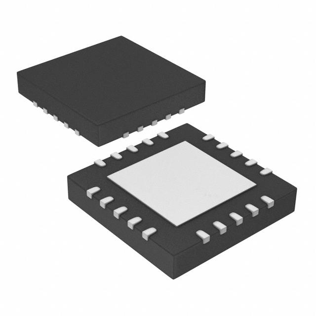
• Package: 20-Lead MQFN
The Microchip Technology Inc. MCP960X/L0X/RL0X
converts thermocouple EMF to degree Celsius with
integrated
cold-junction
compensation.
The
temperature correction coefficients are derived from
the National Institute of Standards and Technology
(NIST) ITS-90 Thermocouple Database. The
MCP9600/01 corrects the thermocouple nonlinear
error characteristics of eight thermocouple types and
outputs ±0.5°C/±1.5°C (Typ./Max.).
Typical Applications
•
•
•
•
•
•
Petrochemical Thermal Management
Hand-Held Measurement Equipment
Industrial Equipment Thermal Management
Commercial and Industrial Ovens
Industrial Engine Thermal Monitor
Temperature Detection Racks
The MCP960X/L0X/RL0X digital temperature sensor
comes with user-programmable registers which
provide design flexibility for various temperature
sensing
applications.
The
registers
allow
user-selectable settings, such as Low-Power modes
for battery powered applications, adjustable digital filter
for fast transient temperatures and four individually
programmable temperature alert outputs which can be
used to detect multiple temperature zones.
In addition, the MCP9601/L01/RL01 family provides
integrated Thermocouple open-circuit and short-circuit
detection features. An alert signal is asserted when the
thermocouple wire is broken or disconnected. Similarly,
alert signal is asserted when the Thermocouple is
shorted to ground or power.
The temperature alert limits have multiple
user-programmable configurations, such as alert
polarity as either an active-low or active-high push-pull
output, and output function as a Comparator mode
(useful for thermostat-type operation) or Interrupt mode
for microprocessor-based systems. In addition, the
alerts can detect either a rising or a falling temperature
with up to +255°C hysteresis.
This sensor uses an industry standard 2-wire, I2C
compatible serial interface and supports up to eight
devices per bus by setting the device address using the
ADDR pin.
PIC® MCU
VDD
VIN+
2
I C
4
Alert
MCP9600/L00/RL00
ADDR
GND
TC+
TC-
VIN-
Types K, J, T,
N, E, B, S, R
2015-2019 Microchip Technology Inc.
DS20005426F-page 1
�MCP960X/L0X/RL0X
20 19 18 17 16
ADDR
GND
GND
20 19 18 17 16
15 Alert 4
GND 1
VIN+ 2
14 Alert 3
VIN+ 2
13 GND
GND 3
EP
21
SCL
5 mm × 5 mm MQFN*
GND 1
GND 3
SDA
MCP9601/L01/RL01
ADDR
GND
5 mm × 5 mm MQFN*
GND
SDA
MCP9600/L00/RL00
SCL
Package Types
15 Alert 4
14 Alert 3
EP
21
13 GND
11 Alert 1
GND 5
11 Alert 1
7
8
9 10
GND
6
OC Alert
9 10
VSENSE
8
GND
7
GND
GND
6
VDD
12 Alert 2
GND 5
SC Alert
VIN- 4
VDD
12 Alert 2
GND
VIN- 4
* Includes Exposed Thermal Pad (EP); see Table 3-1.
MCP960X/L0X/RL0X Block Diagram
ADC Core
+
VIN+
User Registers
Del Sig
Thermocouple Hot-Junction TH
VINError Correction
Junctions Delta Temperature T
∑
Thermocouple Cold-Junction TC
Digital Filter
Thermocouple
Type Selection
Sensor Status
Sensor Configuration
Device Resolution + Power Modes
VSENSE
Alert Config. Registers
Open Circuit
& Short Circuit
Detection
Open Circuit Alert
Alert Registers
Alert 1 Output
Alert 2 Output
Alert 3 Output
Hysteresis Registers
Alert 4 Output
Device ID
Short Circuit Alert
MCP9601/L01/RL01
Only
SCL
I2C Module
SDA
ADDR
2015-2019 Microchip Technology Inc.
DS20005426F-page 2
�MCP960X/L0X/RL0X
1.0
ELECTRICAL CHARACTERISTICS
Absolute Maximum Ratings †
VDD............................................................................................................................................................................ 6.0V
Voltage at All Input/Output Pins ........................................................................................................ GND – 0.3V to 6.0V
Storage Temperature ..............................................................................................................................-65°C to +150°C
Ambient Temperature with Power Applied ..............................................................................................-40°C to +125°C
Junction Temperature (TJ) .................................................................................................................................... +150°C
ESD Protection on All Pins (HBM:MM) .......................................................................................................... (4 kV:300V)
Latch-up Current at Each Pin............................................................................................................................. ±100 mA
† Notice: Stresses above those listed under “Maximum ratings” may cause permanent damage to the device. This is
a stress rating only and functional operation of the device at those or any other conditions above those indicated in
the operational listings of this specification is not implied. Exposure to maximum rating conditions for extended periods
may affect device reliability.
DC CHARACTERISTICS
Electrical Specifications: Unless otherwise indicated, VDD = 2.7V to 5.5V, GND = Ground, TA = -40°C to +125°C
(where: TA = TC, defined as Device Ambient Temperature).
Parameters
Sym.
Min.
Typ.
Max.
-1.5
±0.5
+1.5
-3.0
±1
+3.0
-1.0
±0.5
+1.0
-2.0
±1
+2.0
±0.25
+0.5
Unit
Conditions
Thermocouple Sensor Measurement Accuracy — MCP9600/01
TH Hot-Junction Accuracy (VDD = 3.3V)
TH = TC + T∆ (Note 1)
TH_ACY
TC Cold-Junction Accuracy (VDD = 3.3V)
TC_ACY
°C
°C
TA = 0°C to +85°C,
TA = -40°C to +125°C
TA = 0°C to +85°C
TA = -40°C to +125°C
T∆ Junctions Temperature Delta Accuracy — MCP9600/01
Type K: T∆ = -200°C to +1372°C
VEMF Range: -5.907 mV to 54.886 mV
T∆_ACY
-0.5
°C
TA = 0°C to +85°C,
VDD = 3.3V (Note 2)
Type J: T∆ = -150°C to +1200°C
VEMF Range: -3.336 mV to 47.476 mV
Type T: T∆ = -200°C to +400°C
VEMF Range: -5.603 mV to 20.81 mV
Type N: T∆ = -150°C to +1300°C
VEMF Range: -3.336 mV to 47.476 mV
Type E: T∆ = -200°C to +1000°C
VEMF Range: -8.825 mV to 76.298 mV
Type S: T∆ = 250°C to +1664°C
VEMF Range: -1.875 mV to 17.529 mV
Type B: T∆ = 1000°C to +1800°C
VEMF Range: -4.834 mV to 13.591 mV
TA = 0°C to +85°C,
VDD = 3.3V
(Notes 2, Note 3)
Type R: T∆ = 250°C to +1664°C
VEMF Range: -1.923 mV to 19.732 mV
Note 1
2
3
4
The TC and T summation is implemented in milli-volt (mV) domain. The result, TH (mV), is converted to Degree
Celsius using the NIST ITS-90 Conversion database.
The T_ACY temperature accuracy specification is defined as the device accuracy to the NIST ITS-90
Thermocouple EMF to Degree Celsius Conversion Database. T is also defined as the temperature difference between the hot and cold-junctions or temperatures from the NIST ITS-90 database with TC = 0°C.
The device measures temperature below the specified range, however, the sensitivity to changes in temperature
reduces exponentially. Type R and S measure down to -50°C, or -0.226 mVEMF and -0.235 mVEMF, respectively.
Type B measures down to 500°C or 1.242 mVEMF (see Figures 2-7, 2-8, 2-10, 2-11, 2-14 and 2-17).
Exceeding the VIN_CM input range may cause leakage current through the ESD protection diodes at the
thermocouple input pins. This parameter is characterized but not production tested.
2015-2019 Microchip Technology Inc.
DS20005426F-page 3
�MCP960X/L0X/RL0X
DC CHARACTERISTICS (CONTINUED)
Electrical Specifications: Unless otherwise indicated, VDD = 2.7V to 5.5V, GND = Ground, TA = -40°C to +125°C
(where: TA = TC, defined as Device Ambient Temperature).
Parameters
Sym.
Min.
Typ.
Max.
Unit
Conditions
Thermocouple Sensor Measurement Accuracy — MCP96L00/L01
TH Hot-Junction Accuracy (VDD = 3.3V)
TH = TC + T∆ (Note 1)
TH_ACY
TC Cold-Junction Accuracy (VDD = 3.3V)
TC_ACY
-4.0
±2
+4.0
-6.0
±4
+6.0
-1.0
±0.5
+1.0
-2.0
±1
+2.0
±1.5
+3.0
°C
°C
TA = 0°C to +85°C,
TA = -40°C to +125°C
TA = 0°C to +85°C
TA = -40°C to +125°C
T∆ Junctions Temperature Delta Accuracy — MCP96L00/L01
Type K: T∆ = -200°C to +1372°C
VEMF Range: -5.907 mV to 54.886 mV
T∆_ACY
-3.0
°C
TA = 0°C to +85°C,
VDD = 3.3V (Note 2)
Type J: T∆ = -150°C to +1200°C
VEMF Range: -3.336 mV to 47.476 mV
Type T: T∆ = -200°C to +400°C
VEMF Range: -5.603 mV to 20.81 mV
Type N: T∆ = -150°C to +1300°C
VEMF Range: -3.336 mV to 47.476 mV
Type E: T∆ = -200°C to +1000°C
VEMF Range: -8.825 mV to 76.298 mV
Type S: T∆ = 250°C to +1664°C
VEMF Range: -1.875 mV to 17.529 mV
Type B: T∆ = 1000°C to +1800°C
VEMF Range: -4.834 mV to 13.591 mV
TA = 0°C to +85°C,
VDD = 3.3V
(Notes 2, Note 3)
Type R: T∆ = 250°C to +1664°C
VEMF Range: -1.923 mV to 19.732 mV
Note 1
2
3
4
The TC and T summation is implemented in milli-volt (mV) domain. The result, TH (mV), is converted to Degree
Celsius using the NIST ITS-90 Conversion database.
The T_ACY temperature accuracy specification is defined as the device accuracy to the NIST ITS-90
Thermocouple EMF to Degree Celsius Conversion Database. T is also defined as the temperature difference between the hot and cold-junctions or temperatures from the NIST ITS-90 database with TC = 0°C.
The device measures temperature below the specified range, however, the sensitivity to changes in temperature
reduces exponentially. Type R and S measure down to -50°C, or -0.226 mVEMF and -0.235 mVEMF, respectively.
Type B measures down to 500°C or 1.242 mVEMF (see Figures 2-7, 2-8, 2-10, 2-11, 2-14 and 2-17).
Exceeding the VIN_CM input range may cause leakage current through the ESD protection diodes at the
thermocouple input pins. This parameter is characterized but not production tested.
2015-2019 Microchip Technology Inc.
DS20005426F-page 4
�MCP960X/L0X/RL0X
DC CHARACTERISTICS (CONTINUED)
Electrical Specifications: Unless otherwise indicated, VDD = 2.7V to 5.5V, GND = Ground, TA = -40°C to +125°C
(where: TA = TC, defined as Device Ambient Temperature).
Parameters
Sym.
Min.
Typ.
Max.
Unit
Conditions
Thermocouple Sensor Measurement Accuracy — MCP96RL00/01
TH Hot-Junction Accuracy (VDD = 3.3V)
TH = TC + T∆ (Note 1)
TH_ACY
TC Cold-Junction Accuracy (VDD = 3.3V)
TC_ACY
-8.0
±4
+8.0
-10.0
±6
+10.0
-2.0
±1
+2.0
°C
TA = -40°C to +125°C
±3.0
+6.0
°C
TA = 0°C to +85°C,
VDD = 3.3V (Note 2)
°C
TA = 0°C to +85°C,
TA = -40°C to +125°C
T∆ Junctions Temperature Delta Accuracy — MCP96RL00/01
Type K: T∆ = -200°C to +1372°C
VEMF Range: -5.907 mV to 54.886 mV
T∆_ACY
-6.0
Type J: T∆ = -150°C to +1200°C
VEMF Range: -3.336 mV to 47.476 mV
Type T: T∆ = -200°C to +400°C
VEMF Range: -5.603 mV to 20.81 mV
Type N: T∆ = -150°C to +1300°C
VEMF Range: -3.336 mV to 47.476 mV
Type E: T∆ = -200°C to +1000°C
VEMF Range: -8.825 mV to 76.298 mV
Type S: T∆ = 250°C to +1664°C
VEMF Range: -1.875 mV to 17.529 mV
Type B: T∆ = 1000°C to +1800°C
VEMF Range: -4.834 mV to 13.591 mV
TA = 0°C to +85°C,
VDD = 3.3V
(Notes 2, Note 3)
Type R: T∆ = 250°C to +1664°C
VEMF Range: -1.923 mV to 19.732 mV
Note 1
2
3
4
The TC and T summation is implemented in milli-volt (mV) domain. The result, TH (mV), is converted to Degree
Celsius using the NIST ITS-90 Conversion database.
The T_ACY temperature accuracy specification is defined as the device accuracy to the NIST ITS-90
Thermocouple EMF to Degree Celsius Conversion Database. T is also defined as the temperature difference between the hot and cold-junctions or temperatures from the NIST ITS-90 database with TC = 0°C.
The device measures temperature below the specified range, however, the sensitivity to changes in temperature
reduces exponentially. Type R and S measure down to -50°C, or -0.226 mVEMF and -0.235 mVEMF, respectively.
Type B measures down to 500°C or 1.242 mVEMF (see Figures 2-7, 2-8, 2-10, 2-11, 2-14 and 2-17).
Exceeding the VIN_CM input range may cause leakage current through the ESD protection diodes at the
thermocouple input pins. This parameter is characterized but not production tested.
2015-2019 Microchip Technology Inc.
DS20005426F-page 5
�MCP960X/L0X/RL0X
DC CHARACTERISTICS (CONTINUED)
Electrical Specifications: Unless otherwise indicated, VDD = 2.7V to 5.5V, GND = Ground, TA = -40°C to +125°C
(where: TA = TC, defined as Device Ambient Temperature).
Parameters
Sym.
Min.
Typ.
Max.
Unit
TC and TH Temperature Resolution
TRES
—
±0.0625
—
°C
Sampling Rate (TA = +25°C)
tCONV
—
320
—
—
80
—
—
20
—
Conditions
Sensor Characteristics
With max. resolution
18-bit resolution
ms
16-bit resolution
14-bit resolution
—
5
—
tCALC
—
12
—
ms
Offset Error
VOERR
—
±2
—
µV
Offset Error Drift
VOE_DR
—
50
—
nV/°C
GERR
—
—
±0.04
Full-Scale Gain Error — MCP96L00/L01
—
±0.12
—
Full-Scale Gain Error — MCP96RL00/RL01
—
±0.24
—
GER_DR
—
±0.01
—
%FS
INL
—
10
—
ppm
VRES
—
2
—
µV
18-bit resolution
Differential Mode Range
VIN_DF
-250
—
+250
mV
ADC input range
Differential Mode Impedance
ZIN_DF
—
300
—
k
Common-Mode Range
VIN_CM VDD – 0.3
—
VDD + 0.3
V
Common-Mode Impedance
ZIN_CM
—
25
—
M
Common-Mode Rejection Ratio
CMRR
—
105
—
dB
Power Supply Rejection Ratio
PSRR
—
60
—
dB
Line Regulation
VLine_R
—
0.2
—
°C/V
Temperature Calculation Time
12-bit resolution
TA = +25°C
Thermocouple Input
Full-Scale Gain Error — MCP9600/01
Full-Scale Gain Error Drift
Full-Scale Integral Nonlinearity
Voltage Resolution
TA = 0°C to +85°C
%FS
TA = -40°C to +125°C
(Note 4)
Voltage Sense Input (VSENSE) for Thermocouple Open and Short-Circuit Detection (MCP9601/L01/RL01)
VSENSE Input Range
- Range: Short Circuit to VDD
VSiRNG
0
—
100
(see Figure 1-1)
VSiSC
90
—
100
SC Alert asserts
0
—
10
- Range: Short Circuit to GND
%VDD
- Range: Open Circuit
VSiOC
58
—
75
OC Alert asserts
- Range: Normal Operation
VSiNOR
40
—
58
OC Alert deasserts
Note 1
2
3
4
The TC and T summation is implemented in milli-volt (mV) domain. The result, TH (mV), is converted to Degree
Celsius using the NIST ITS-90 Conversion database.
The T_ACY temperature accuracy specification is defined as the device accuracy to the NIST ITS-90
Thermocouple EMF to Degree Celsius Conversion Database. T is also defined as the temperature difference between the hot and cold-junctions or temperatures from the NIST ITS-90 database with TC = 0°C.
The device measures temperature below the specified range, however, the sensitivity to changes in temperature
reduces exponentially. Type R and S measure down to -50°C, or -0.226 mVEMF and -0.235 mVEMF, respectively.
Type B measures down to 500°C or 1.242 mVEMF (see Figures 2-7, 2-8, 2-10, 2-11, 2-14 and 2-17).
Exceeding the VIN_CM input range may cause leakage current through the ESD protection diodes at the
thermocouple input pins. This parameter is characterized but not production tested.
2015-2019 Microchip Technology Inc.
DS20005426F-page 6
�MCP960X/L0X/RL0X
DC CHARACTERISTICS (CONTINUED)
Electrical Specifications: Unless otherwise indicated, VDD = 2.7V to 5.5V, GND = Ground, TA = -40°C to +125°C
(where: TA = TC, defined as Device Ambient Temperature).
Parameters
VSENSE Input Leakage
Sym.
Min.
Typ.
Max.
Unit
ISiLEAK
—
0.1
1
µA
Conditions
Alert 1, 2, 3, 4 Outputs, SC Alert and OC Alert Outputs (MCP9601/L01/RL01)
Low-Level Voltage
VOL
—
—
0.4
V
IOL= 3 mA
High-Level Voltage
VOH
VDD – 0.5
—
—
V
IOH= 3 mA
Operating Voltage
VDD
2.7
—
5.5
V
I2
IDD
—
0.3
0.5
mA
—
1.5
2.5
mA
Operating Voltage and Current
C Inactive Current
I2
C Active Current or During tCALC
VDD = 3.3V,
TA = +85°C
Shutdown Current
ISHDN
—
2
5
µA
I2C inactive,
TA = +85°C
Power-on Reset (POR) Thresholds
VPOR
1.0
2.1
2.6
V
Rising/Falling VDD
tRSP
—
3
—
s
+25°C (air) to +125°C
(oil bath), 2x2” PCB
Thermal Response
Package Thermal Response
(Time to 63% of Final Temperature)
Note 1
2
3
4
The TC and T summation is implemented in milli-volt (mV) domain. The result, TH (mV), is converted to Degree
Celsius using the NIST ITS-90 Conversion database.
The T_ACY temperature accuracy specification is defined as the device accuracy to the NIST ITS-90
Thermocouple EMF to Degree Celsius Conversion Database. T is also defined as the temperature difference between the hot and cold-junctions or temperatures from the NIST ITS-90 database with TC = 0°C.
The device measures temperature below the specified range, however, the sensitivity to changes in temperature
reduces exponentially. Type R and S measure down to -50°C, or -0.226 mVEMF and -0.235 mVEMF, respectively.
Type B measures down to 500°C or 1.242 mVEMF (see Figures 2-7, 2-8, 2-10, 2-11, 2-14 and 2-17).
Exceeding the VIN_CM input range may cause leakage current through the ESD protection diodes at the
thermocouple input pins. This parameter is characterized but not production tested.
VDD
RA
RB
VSENSE
+
VIN+
Del Sig
Where:
C
VIN-
MCP9601/L01/RL01
FIGURE 1-1:
Thermocouple
RB
RA = 1 M ± 5% Tolerance (Max.)
RB = 2 M ± 20% Range
C = 0.1 µF
Open and Short Circuit Detection Configuration.
2015-2019 Microchip Technology Inc.
DS20005426F-page 7
�MCP960X/L0X/RL0X
INPUT/OUTPUT PIN DC CHARACTERISTICS
Electrical Specifications: Unless otherwise indicated, VDD = 2.7V to 5.5V, GND = Ground, TA = -40°C to +125°C
(where: TA = TC, defined as Device Ambient Temperature).
Parameters
Sym.
Min.
Typ.
Max.
Units
V
Conditions
2
Serial Input/Output and I C Slave Address Input (ADDR)
Input (SCL, SDA, ADDR)
High-Level Voltage
Low-Level Voltage
VIH
0.7 × VDD
—
—
VIL
—
—
0.3 × VDD
V
Input Current
ILEAK
—
—
±2
µA
Hysteresis
VHYST
—
0.05 × VDD
—
V
TSP
—
50
—
ns
Low-Level Voltage
VOL
—
—
0.4
V
IOL= 3 mA
High-Level Current (leakage)
IOH
—
—
1
µA
VOH = VDD
Low-Level Current
IOL
6
—
—
mA
VOL = 0.6V
Capacitance
CIN
—
5
—
pF
V
Spike Suppression
VDD > 2V
Output (SDA)
I2C Slave Address Selection Levels (Note 1)
Command Byte [1100 000x]
GND
—
—
VADDR_L
VADDR_TYP
VADDR_H
(Note 2)
(Note 2)
(Note 2)
VADDR
Command Byte [1100 001x]
Command Byte [1100 010x]
Command Byte [1100 011x]
Address = 0
Address = 1
Address = 2
Address = 3
Command Byte [1100 100x]
Address = 4
Command Byte [1100 101x]
Address = 5
Command Byte [1100 110x]
Address = 6
Command Byte [1100 111x]
Note 1
2
—
—
Address = 7
VDD
The ADDR pin can be tied to VDD or VSS. For additional slave addresses, a resistive divider network can
be used to set voltage levels that are rationed to VDD. The device supports up to eight levels (see
Section 6.3.1 “I2C Addressing” for recommended resistor values).
VADDR_TYP = Address * VDD/8 + VDD/16,
VADDR_L = VADDR_TYP – VDD/32 and
VADDR_H = VADDR_TYP + VDD/32 (where: Address = 1, 2, 3, 4, 5, 6).
TEMPERATURE CHARACTERISTICS
Electrical Specifications: Unless otherwise indicated, VDD = 2.7V to 5.5V, GND = Ground.
Parameters
Sym.
Min.
Typ.
Max.
Units
Specified Temperature Range
TA
-40
—
+125
°C
Operating Temperature Range
TA
-40
—
+125
°C
Storage Temperature Range
TA
-65
—
+150
°C
JA
—
38.8
—
°C/W
Conditions
Temperature Ranges
(Note 1)
Thermal Package Resistances
Thermal Resistance, MQFN
Note 1
Operation in this range must not cause TJ to exceed the Maximum Junction Temperature (+150°C).
2015-2019 Microchip Technology Inc.
DS20005426F-page 8
�MCP960X/L0X/RL0X
SENSOR SERIAL INTERFACE TIMING SPECIFICATIONS
Electrical Specifications: Unless otherwise indicated, GND = Ground, TA = -40°C to +125°C, VDD = 2.7V to 5.5V
and CL = 80 pF (Note 1).
Parameters
Sym.
Min.
Max.
Units
2
2-Wire I C Interface
Serial Port Frequency
fSCL
10
100
kHz
Low Clock (Note 2)
tLOW
4700
—
ns
High Clock
tHIGH
4000
—
ns
tR
—
1000
ns
Rise Time (Note 3)
Fall Time (Note 3)
tF
20
300
ns
Data in Setup Time (Note 2)
tSU:DAT
250
—
ns
Data in Hold Time
tHD:DAT
0
—
ns
Start Condition Setup Time
tSU:STA
4700
—
ns
Start Condition Hold Time
tHD:STA
4000
—
ns
Stop Condition Setup Time
tSU:STO
4000
—
ns
Bus Idle/Free
tB-FREE
10
—
µs
Cb
—
400
pf
tSTRETCH
60
—
µs
Bus Capacitive Load
Clock Stretching (Note 4)
P
RE
E
TO
-F
U
-S
tB
tL
I
DD
tH
tS
U
-D
AT
A
tR
,t
F
SD
A
SC
L
tS
tS
IG
H
tH
TR
ET
O
W
H
C
AC
K
D
-S
tH
tS
U
-S
TA
RT
3
4
All values referred to VIL MAX and VIH MIN levels.
This device can be used in a Standard mode I2C bus system, but the requirement, tSU:DAT 250 ns, must
be met.
Characterized, but not production tested.
Master controllers without features to detect clock stretching by Slave devices, should reduce fSCL for
proper I2C communication for Read commands. See Figure 2-29 for a typical tSTRETCH performance.
TA
RT
Note 1
2
Start Condition
FIGURE 1-2:
Data Transmission
Stop Condition
Timing Diagram.
2015-2019 Microchip Technology Inc.
DS20005426F-page 9
�MCP960X/L0X/RL0X
2.0
TYPICAL PERFORMANCE CURVES
Note:
The graphs and tables provided following this note are a statistical summary based on a limited number of
samples and are provided for informational purposes only. The performance characteristics listed herein
are not tested or guaranteed. In some graphs or tables, the data presented may be outside the specified
operating range (e.g., outside specified power supply range) and therefore, outside the warranted range.
Note: Unless otherwise indicated, VDD = 2.7V to 5.5V, GND = Ground, SDA/SCL pulled-up to VDD and
TA = -40°C to +125°C.
0.500
Type K
MCP9600
Type K
MCP9600/L00/RL00
0.25
Sensitivity ('
'°C/LSb)
Temperature Accuracy (°C)
0.50
0.00
-0.25
-0.50
-200
300
800
1300
0.250
0.000
-200
1800
300
TA (°C)
FIGURE 2-1:
Typical Temperature
Accuracy from NIST ITS-90 Database, Type K.
Sensitivity ('
'°C/LSb)
7HPSHUDWXUH�$FFXUDF\��&�
����
����
�����
���
���
����
Type J
MCP9600/L00/RL00
0.250
0.000
-200
����
300
7$ �&�
FIGURE 2-2:
Typical Temperature
Accuracy from NIST ITS-90 Database, Type J.
800
TA (°C)
1300
1800
FIGURE 2-5:
Temperature Sensitivity with
18-Bit Resolution, Type J.
����
0.500
7\SH�1
0&3����
����
Sensitivity ('
'°C/LSb)
7HPSHUDWXUH�$FFXUDF\��&�
1800
0.500
7\SH�0&3����
����
�����
�����
����
1300
FIGURE 2-4:
Temperature Sensitivity with
18-Bit Resolution, Type K.
����
�����
����
800
TA (°C)
���
���
����
����
7$ �&�
FIGURE 2-3:
Typical Temperature
Accuracy from NIST ITS-90 Database, Type N.
2015-2019 Microchip Technology Inc.
Type N
MCP9600/L00/RL00
0.250
0.000
-200
300
800
1300
1800
TA (°C)
FIGURE 2-6:
Temperature Sensitivity with
18-Bit Resolution, Type N.
DS20005426F-page 10
�MCP960X/L0X/RL0X
Note: Unless otherwise indicated, VDD = 2.7V to 5.5V, GND = Ground, SDA/SCL pulled-up to VDD and
TA = -40°C to +125°C.
0.500
7\SH�6
0&3����
����
Sensitivity ('
'°C/LSb)
7HPSHUDWXUH�$FFXUDF\��&�
����
6SHFLILHG�5DQJH
����
�����
�����
����
���
���
����
Type S
MCP9600/L00/RL00
Specified Range
0.250
0.000
-200
����
300
7$ �&�
FIGURE 2-7:
Typical Temperature
Accuracy from NIST ITS-90 Database, Type S.
Sensitivity ('
'°C/LSb)
7HPSHUDWXUH�$FFXUDF\��&�
6SHFLILHG�5DQJH
����
�����
���
���
����
Type R
MCP9600/L00/RL00
Specified Range
0.250
0.000
-200
����
300
7$ �&�
FIGURE 2-8:
Typical Temperature
Accuracy from NIST ITS-90 Database, Type R.
1300
1800
0.500
Type E
MCP9600
Type E
MCP9600/L00/RL00
0.25
Sensitivity ('
'°C/LSb)
Temperature Accuracy (°C)
800
TA (°C)
FIGURE 2-11:
Temperature Sensitivity with
18-Bit Resolution, Type R.
0.50
0.00
-0.25
-0.50
-200
1800
0.500
7\SH�5
0&3����
�����
����
1300
FIGURE 2-10:
Temperature Sensitivity with
18-Bit Resolution, Type S.
����
����
800
TA (°C)
300
800
1300
1800
TA (°C)
FIGURE 2-9:
Typical Temperature
Accuracy from NIST ITS-90 Database, Type E.
2015-2019 Microchip Technology Inc.
0.250
0.000
-200
300
800
TA (°C)
1300
1800
FIGURE 2-12:
Temperature Sensitivity with
18-Bit Resolution, Type E.
DS20005426F-page 11
�MCP960X/L0X/RL0X
Note: Unless otherwise indicated, VDD = 2.7V to 5.5V, GND = Ground, SDA/SCL pulled-up to VDD and
TA = -40°C to +125°C.
0.500
Type T
MCP9600
0.25
Sensitivity ('
'°C/LSb)
Temperature Accuracy (°C)
0.50
0.00
-0.25
-0.50
-200
300
800
1300
Type T
MCP9600/L00/RL00
0.250
0.000
-200
1800
300
800
TA (°C)
TA (°C)
FIGURE 2-13:
Typical Temperature
Accuracy from NIST ITS-90 Database, Type T.
Sensitivity ('
'°C/LSb)
Temperature Accuracy (°C)
0.500
Type B
MCP9600
Specified Range
0.00
-0.25
-0.50
-200
300
800
1300
Type B
MCP9600/L00/RL00
Specified Range
0.250
0.000
-200
1800
300
TA (°C)
FIGURE 2-14:
Typical Temperature
Accuracy from NIST ITS-90 Database, Type B.
800
TA (°C)
1300
1800
FIGURE 2-17:
Temperature Sensitivity with
18-Bit Resolution, Type B.
0.4
10
Gain Error (% of FSR)
MCP9600
Offset Error (µV)
1800
FIGURE 2-16:
Temperature Sensitivity with
18-Bit Resolution, Type T.
0.50
0.25
1300
5
0
-5
-10
VDD = 3.3V
MCP9600
0.3
0.2
0.1
0
-0.1
-0.2
-0.3
-0.4
-40
-20
0
20
40
60
80
100
120
-40
-20
Temperature (°C)
FIGURE 2-15:
(VIN+, VIN-).
Input Offset Error Voltage
2015-2019 Microchip Technology Inc.
0
20
40
60
80
100 120
Temperature (°C)
FIGURE 2-18:
Full-Scale Gain Error.
DS20005426F-page 12
�MCP960X/L0X/RL0X
Note: Unless otherwise indicated, VDD = 2.7V to 5.5V, GND = Ground, SDA/SCL pulled-up to VDD and
TA = -40°C to +125°C.
0.005
Integral Nonlinearity (% of FSR)
10.0
TA = +25°C
5.0
2.5
0.0
-100
-75
-50 -25
0
25
50
Input Voltage (% of Full-Scale)
FIGURE 2-19:
75
Input Noise,% of Full Scale.
0.001
0.000
���
���
2FFXUUHQFHV
���
���9
$YHUDJH
����
3.0
FIGURE 2-22:
VDD.
9''� ����9
����XQLWV�DW����&�����&������&
���XQLWV�DW�RWKHU�WHPSHUDWXUHV
6SHF /LPLW
3.5
4.0
VDD (V)
4.5
5.0
5.5
Integral Nonlinearity Across
7$ ����&�WR�����&
9'' ����9
�����XQLWV
0&3����
���
���
�6WG��'HY�
6WGHY�
6WGHY�
�6WG��'HY�
FIGURE 2-20:
Cold-Junction Sensor
Temperature Accuracy.
400
300
���
���
���
���
���
���
7HPSHUDWXUH�$FFXUDF\��&�
FIGURE 2-23:
Cold-Junction Sensor
Temperature Accuracy Distribution.
T-40C
A = -40°C
35C
TA = +35°C
85C
TA = +85°C
125C
TA = +125°C
SDA, and Alert 1, 2, 3, 4 outputs
����
����
���
�
��
��
��
�� ��� ���
7ǻ 7HPSHUDWXUH��,76����'DWDEDVH��&�
200
500
T-40C
A = -40°C
35C
TA = +35°C
85C
TA = +85°C
125C
TA = +125°C
Alert 1, 2, 3, 4 outputs
400
VDD - VOH (µA)
���
����
��
����
����
7ǻB$&< �&�
0.002
2.5
���
VOL (µA)
0.003
100
���
0&3����
0.004
����
Noise (µV, rms)
7.5
300
200
100
100
0
2.5
3.0
FIGURE 2-21:
Across VDD.
3.5
4.0
VDD (V)
4.5
5.0
5.5
SDA and Alert Outputs, VOL
2015-2019 Microchip Technology Inc.
2.5
3.0
FIGURE 2-24:
VDD.
3.5
4.0
VDD (V)
4.5
5.0
5.5
Alert Outputs, VOH Across
DS20005426F-page 13
�MCP960X/L0X/RL0X
Note: Unless otherwise indicated, VDD = 2.7V to 5.5V, GND = Ground, SDA/SCL pulled-up to VDD and
TA = -40°C to +125°C.
500
2.0
400
85C
TA = +85°C
300
TA = +125°C
125C
1.0
TA = -40°C
-40C
35C
TA = +35°C
85C
TA = + 85°C
125C
TA = +125°C
200
100
2.5
3.0
3.5
4.0
VDD (V)
4.5
5.0
0.0
2.5
5.5
I2C Inactive, IDD Across VDD.
FIGURE 2-25:
-40C
TA = -40°C
35C
TA = +35°C
85C
TA = + 85°C
125C
TA = +125°C
1500
1000
3.5
4.0
VDD (V)
4.5
5.0
5.5
T-40C
A = -40°C
TA = +35°C
35C
85C
TA = +85°C
125C
TA = +125°C
40.0
tSTRETCH (µs)
2000
3.0
FIGURE 2-28:
SDA, SCL and ADDR Input
Pins Leakage Current, ILEAK Across VDD.
60.0
2500
I2C Active, IDD (µA)
T-40C
A = -40°C
35C
TA = +35°C
ILEAK (µA)
I2C Inactive, IDD (µA)
ADDR/SDA/SCL pins
20.0
0.0
500
2.5
3.0
FIGURE 2-26:
���
3.5
4.0
VDD (V)
4.5
5.0
2.5
5.5
I2C Active, IDD Across VDD.
2.0%
ΔtCALC (%)
1.0%
,6+'1 �$�
���
���
3.5
4.0
VDD (V)
4.5
5.5
Conditions:
tCALC = 12 ms (typical)
VDD = 3.3V
TA = Room Temperature
0.0%
-40C
TA = -40°C
35C
TA = +35°C
85C
TA = + 85°C
125C
TA = +125°C
-1.0%
���
5.0
FIGURE 2-29:
I2C Interface Clock Stretch
Duration, tSTRETCH Across VDD.
����&
7$ ����&
��&
7$ ����&
��&
7$ �����&
���&
7$ �����&
���
3.0
-2.0%
���
���
���
FIGURE 2-27:
Across VDD.
���
���
9'' �9�
���
���
���
Shutdown Current, ISHDN
2015-2019 Microchip Technology Inc.
2.5
3.0
3.5
4.0
VDD (V)
4.5
5.0
5.5
FIGURE 2-30:
Temperature Calculation
Duration, tCALC Change Across VDD.
DS20005426F-page 14
�MCP960X/L0X/RL0X
3.0
PIN DESCRIPTIONS
The descriptions of the pins are listed in Table 3-1.
TABLE 3-1:
PIN FUNCTION TABLE
MCP9600/L00/RL00 MCP9601/L01/RL01
1, 3, 5,13, 17
3.1
Symbol
Pin Function
1, 3, 5, 13, 17
GND
Electrical Ground
2
2
VIN+
Thermocouple Positive Terminal Input
4
4
VIN-
Thermocouple Negative Terminal Input
6, 7, 9, 10, 18
10, 18
GND
—
6
VSENSE
—
7
SC Alert
8
8
VDD
Not Electrical Ground; must be tied to Ground
Thermocouple Open and Short Circuit detection input
Thermocouple Short Circuit Alert Output
Power
—
9
OC Alert
11
11
Alert 1
Alert Output 1
12
12
Alert 2
Alert Output 2
14
14
Alert 3
Alert Output 3
15
15
Alert 4
Alert Output 4
16
16
ADDR
I2C Save Address Selection Voltage Input
19
19
SCL
I2C Clock Input
20
20
SDA
I2C Data Input
21
21
EP
Ground Pin (GND)
Thermocouple Open Circuit Alert Output
Exposed Thermal Pad (EP); must be connected to GND
3.5
I2C Slave Address Pin (ADDR)
The GND pin is the system ground pin. Pins 1, 3, 5, 13
and 17 are system ground pins and they are at the
same potential. However, pins 6, 7, 9, 10 and 18 must
be connected to ground for normal operation.
This pin is used to set the I2C slave address. This pin
can be tied to VDD, GND, or a ratio of VDD can be
selected to set up to eight address levels using a
resistive voltage divider network.
3.2
3.6
Thermocouple Input (VIN+, VIN-)
The thermocouple wires are directly connected to
these inputs. The positive node is connected to the
VIN+ pin, while the negative node connects to the VINnode. The thermocouple voltage is converted to degree
Celsius.
3.3
Power Pin (VDD)
Serial Clock Line (SCL)
The SCL is a clock input pin. All communication and
timing is relative to the signal on this pin. The clock is
generated by the host or master controller on the bus
(see Section 4.0 “Serial Communication”).
3.7
Serial Data Line (SDA)
VDD is the power pin. The operating voltage range, as
specified in the DC Characteristics table, is applied on
this pin.
SDA is a bidirectional input/output pin used to serially
transmit data to/from the host controller. This pin
requires a pull-up resistor (see Section 4.0 “Serial
Communication”).
3.4
3.8
Push-Pull Alert Outputs
(Alert 1, 2, 3, 4 and OC/SC Alert)
The Alert pins are user-programmable push-pull outputs
which can be used to detect rising or falling
temperatures. The device outputs signal when the
ambient temperature exceeds the user-programmed
temperature alert limit.
The OC Alert and the SC Alert outputs are also
active-high push-pull outputs (MCP9601/L01/RL01).
These outputs are asserted when Open-Circuit and
Short-Circuit conditions are detected on the VSENSE pin.
2015-2019 Microchip Technology Inc.
Thermocouple Open/Short
Detection Input (VSENSE)
The VSENSE pin is a thermocouple detection input pin
(MCP9601/L01/RL01) and the voltage level on this pin
is used to determine whether the thermocouple is operating normally, shorted to VDD/VSS, or it is disconnected from the VIN+ and VIN- pins (see Figure 1-1).
DS20005426F-page 15
�MCP960X/L0X/RL0X
4.0
SERIAL COMMUNICATION
4.1
2-Wire Standard Mode I2C
Protocol-Compatible Interface
The MCP960X/L0X/RL0X Serial Clock Input (SCL) and
the bidirectional Serial Data Line (SDA) form a 2-wire
bidirectional data communication line (refer to the
Input/Output Pin DC Characteristics table and
Sensor Serial Interface Timing Specifications
table).
The following bus protocol has been defined:
TABLE 4-1:
Term
MCP9600/L00/RL00
SERIAL BUS PROTOCOL
DESCRIPTIONS
Description
Master
The device that controls the serial bus,
typically a microcontroller
Slave
The device addressed by the master,
such as the MCP960X/L0X/RL0X
Transmitter Device sending data to the bus
Receiver
Device receiving data from the bus
START
A unique signal from master to initiate
serial interface with a slave
STOP
A unique signal from the master to
terminate serial interface from a slave
Read/Write A read or write to the
MCP960X/L0X/RL0X registers
ACK
A receiver Acknowledges (ACK) the
reception of each byte by polling the
bus
NAK
A receiver Not Acknowledges (NAK) or
releases the bus to show End-of-Data
(EOD)
Busy
Communication is not possible
because the bus is in use
Not Busy
The bus is in the Idle state, both SDA
and SCL remain high
Data Valid
SDA must remain stable before SCL
becomes high in order for a data bit to
be considered valid. During normal
data transfers, SDA only changes state
while SCL is low.
4.1.1
DATA TRANSFER
Data transfers are initiated by a Start condition
(START), followed by a 7-bit device address and a
read/write bit. An Acknowledge (ACK) from the slave
confirms the reception of each byte. Each access must
be terminated by a Stop condition (STOP).
Repeated communication is initiated after tB-FREE.
2015-2019 Microchip Technology Inc.
This device supports the Receive Protocol. The
register can be specified using the pointer for the initial
read. Each repeated read or receive begins with a Start
condition and address byte. The MCP960X/L0X/RL0X
retains the previously selected register. Therefore, it
outputs data from the previously-specified register
(repeated pointer specification is not necessary).
4.1.2
MASTER/SLAVE
The bus is controlled by a master device (typically a
microcontroller) that controls the bus access, and
generates the Start and Stop conditions. The
MCP960X/L0X/RL0X is a slave device and does not
control other devices in the bus. Both master and slave
devices can operate as either transmitter or receiver.
However, the master device determines which mode is
activated.
4.1.3
START/STOP CONDITION
A high-to-low transition of the SDA line (while SCL is
high) is the Start condition. All data transfers must be
preceded by a Start condition from the master. A
low-to-high transition of the SDA line (while SCL is
high) signifies a Stop condition.
If a Start or Stop condition is introduced during data
transmission, the MCP960X/L0X/RL0X releases the
bus. All data transfers are ended by a Stop condition
from the master.
4.1.4
ADDRESS BYTE
Following the Start condition, the host must transmit an
8-bit address byte to the MCP960X/L0X/RL0X. The
address for the MCP960X/L0X/RL0X temperature sensor
is ‘11,0,0,A2,A1,A0’ in binary, where the A2, A1 and
A0 bits are set externally by connecting the corresponding
VADDR voltage levels on the ADDR pin (see the
“Input/Output Pin DC Characteristics” section). The
7-bit address transmitted in the serial bit stream must
match the selected address for the MCP960X/L0X/RL0X
to respond with an ACK. Bit 8 in the address byte is a
read/write bit. Setting this bit to ‘1’ commands a read operation, while ‘0’ commands a write operation (see
Figure 4-1).
Command Byte
1
SCL
SDA
2
1 1
Start
3
4
5
6
7
0
0 A2 A1 A0
8
9
A
C
K
Slave
Address R/W
MCP960X/L0X/RL0X Response
FIGURE 4-1:
Device Addressing.
DS20005426F-page 16
�MCP960X/L0X/RL0X
4.1.5
DATA VALID
After the Start condition, each bit of data in
transmission needs to be settled for a time specified by
tSU-DATA before SCL toggles from low-to-high (see the
“Sensor Serial Interface Timing Specifications”
section).
4.1.6
ACKNOWLEDGE (ACK/NAK)
Each receiving device, when addressed, is expected to
generate an ACK bit after the reception of each byte.
The master device must generate an extra clock pulse
for ACK to be recognized.
The Acknowledging device pulls down the SDA line for
tSU-DATA before the low-to-high transition of SCL from
the master. SDA also needs to remain pulled down for
tHD-DAT after a high-to-low transition of SCL.
During read, the master must signal an End-of-Data
(EOD) to the slave by not generating an ACK bit (NAK)
once the last bit has been clocked out of the slave. In
this case, the slave will leave the data line released to
enable the master to generate the Stop condition.
4.1.7
CLOCK STRETCHING
2
During the I C read operation, this device will hold the
I2C clock line low for tSTRECH after the falling edge of
the ACK signal. In order to prevent bus contention, the
master controller must release or hold the SCL line low
during this period.
Note:
If the master controller does not provide
the adequate delay as specified by
tSTRECH, then the device will output the
previously transmitted data.
In addition, the master controller must provide eight
consecutive clock cycles after generating the ACK bit
from a read command. This allows the device to push
out data from the SDA Output Shift registers. Missing
clock cycles could result in bus contention. At the end
of one or more data transmission, the master controller
must provide the NAK bit, followed by a Stop Condition
to terminate communication (see Figure 4-3).
MCP9600/L00/RL00 Clock Stretching – tSTRETCH
7
A
0
8
R
1
A
C
K
x
2
3
x
x
4
x
5
x
6
x
7
x
8
x
A
C
K
TH MSB Data
Master
MCP960X/L0X/RL0X
FIGURE 4-2:
4.1.8
Clock Stretching.
SEQUENTIAL READ
During a sequential read, the device transmits data
bytes starting from the previously set Register Pointer.
The MCP960X/L0X/RL0X increments an internal
address pointer each time a byte transmission is successfully completed with an ACK bit from the master
controller. Therefore, the device can sequentially output the entire register values shown in Table 5-1 (see
Figure 4-6). A Stop Condition terminates the sequential read.
2015-2019 Microchip Technology Inc.
DS20005426F-page 17
�MCP960X/L0X/RL0X
1
2
3
4
5
6
7
8
1
2
3
4
5
6
7
8
SCL
SDA
S
1
1
0
A
2
0
A
1
A
0
A
W C
0
K
Address Byte
0
0
0
0
0
0
Pointer
(Table 4-2)
Slave*
A
C P
K
0
Slave*
MCP960X/L0X/RL0X Clock Stretching, tSTRETCH
1
2
3
4
5
6
7
8
1
2
3
4
5
6
7
8
1
2
3
4
5
6
7
8
SCL
SDA
S
1
1
0
0
A
2
A
1
A
0
Address Byte
A
R C
0
K
Slave*
0
0
0
0
0
0
MSB Data
1
A
C
K
1
Master
0
0
1
0
1
0
LSB Data
0
N
A
K
P
Master
*MCP960X/L0X/RL0X
TABLE 4-2:
POINTERS
Read-Only
Registers
Pointer
TH
0000 0000
T∆
0000 0001
TC
0000 0010
Note: this is an example pseudo routine:
i2c_start();
// send START command
i2c_write(b’1100 0000’);
// WRITE Command
// also, make sure bit 0 is cleared ‘0’
i2c_write(b’0000 00XX’);
// Write TH, T∆, or TC registers
i2c_stop();
// send STOP command
i2c_start();
// send START command
i2c_write(b’1100 0001’);
// READ Command
// also, make sure bit 0 is set ‘1’
UpperByte = i2c_read(ACK);
// READ 8 bits (with tSTRETCH delay)
// and Send ACK bit
LowerByte = i2c_read(NAK);
// READ 8 bits (with tSTRETCH delay)
// and Send NAK bit
i2c_stop();
// send STOP command
//Convert the temperature data
if ((UpperByte & 0x80) == 0x80){
//Temperature 0°C
Temperature = (UpperByte x 16 + LowerByte / 16) - 4096;
}else
//Temperature 0°C
Temperature = (UpperByte x 16 + LowerByte / 16);
//TH, TD, or TC Temperature (°C) depending on the register pointer value shown in Table 4-2.
FIGURE 4-3:
Timing Diagram to Set a Register Pointer and Read a Two-Byte Data.
2015-2019 Microchip Technology Inc.
DS20005426F-page 18
�MCP960X/L0X/RL0X
1
2
3
4
5
6
7
8
1
2
3
4
5
6
7
8
1
2
3
4
5
6
7
8
SCL
SDA
S
1
1
0
0
A
2
A
1
A
C
K
A W
0
0
0
0
0
1
0
A
C
K
1
Configuration
(Table 4-3)
Slave*
Address Byte
0
x
x
Slave*
x
x
x
x
x
x
A
C
K
P
Register Data
MCP960X/L0X/RL0X Clock Stretching, tSTRETCH
1
2
3
4
5
6
7
8
1
2
3
4
5
6
7
8
SCL
SDA
S
1
1
0
A
0 A A A R C
2 1 0
K
Address Byte
TABLE 4-3:
x x
Slave*
x
x
x
x
N
x A P
K
Master
LSB Data
POINTERS
Read/Write
Registers
Pointer
STATUS
0000 0100
Configuration
x
*MCP960X/L0X/RL0X
0000 0101
0000 0110
Note: this is an example pseudo routine:
i2c_start();
// send START command
i2c_write(b’1100 0000’);
// WRITE Command
// also, make sure bit 0 is cleared ‘0’
i2c_write(b’0000 0101’);
// Write Status or Configuration registers
i2c_write(b’XXXX XXXX’);
// Write register data
i2c_stop();
// send STOP command
i2c_start();
// send START command
i2c_write(b’1100 0001’);
// READ Command
// also, make sure bit 0 is set ‘1’
Data = i2c_read(NAK);
// READ 8 bits (with tSTRETCH delay)
// and Send NAK bit
i2c_stop();
FIGURE 4-4:
// send STOP command
Timing Diagram to Set a Register Pointer, Write One Byte, and Read the Data.
2015-2019 Microchip Technology Inc.
DS20005426F-page 19
�MCP960X/L0X/RL0X
1
2
3
4
5
6
7
8
1
2
3
4
5
6
7
8
1
2
3
4
5
6
7
8
SCL
SDA
S
1
1
0
0
A
2
A
1
A
A W C
0
K
0
0
0
Slave*
Address Byte
1
0
0
0
A
C
K
0
x
x
x
x
1
2
x
x
3
Slave*
4
x
x
A
C
K
x
x
Alert 1 MSB
Slave*
Alert Limit 1
(Table 4-4)
x
x
5
6
x
x
7
x
8
x
A
C P
K
Slave*
Alert 1 LSB
MCP960X/L0X/RL0X Clock Stretching, tSTRETCH
1
2
3
4
5
6
7
8
1
2
3
4
5
6
7
8
1
2
3
4
5
6
7
8
SCL
SDA
S
1
1
0
0
A
2
A
1
Address Byte
TABLE 4-4:
A
0
A
R C
K
x
x
x
Slave*
x
x
x
x
Alert 1 MSB
x
A
C
K
Pointer
Alert 1
0001 0000
Alert 2
0001 0001
Alert 3
0001 0010
Alert 4
0001 0011
x
x
x
x
x
x
Alert 1 LSB
Master
x
N
A
K
P
Master
*MCP960X/L0X/RL0X
POINTERS
Alert Limit
Registers
x
Note: this is an example pseudo routine:
i2c_start();
// send START command
i2c_write(b’1100 0000’);
//WRITE Command
//also, make sure bit 0 is cleared ‘0’
i2c_write(b’0001 00XX’);
// Write Alert registers
i2c_write(b’XXXX XXXX’);
// Write register Upper Byte
i2c_write(b’XXXX XXXX’);
// Write register Lower Byte
i2c_stop();
// send STOP command
i2c_start();
// send START command
i2c_write(b’1100 0001’);
//READ Command
//also, make sure bit 0 is set ‘1’
UpperByte = i2c_read(ACK);
// READ 8 bits (with tSTRETCH delay)
//and Send ACK bit
LowerByte = i2c_read(NAK);
// READ 8 bits (with tSTRETCH delay)
//and Send NAK bit
i2c_stop();
FIGURE 4-5:
// send STOP command
Timing Diagram to Set a Register Pointer, Write Two Bytes, and Read the Data.
2015-2019 Microchip Technology Inc.
DS20005426F-page 20
�MCP960X/L0X/RL0X
1
2
3
4
5
6
7
8
1
2
3
4
5
6
7
8
SCL
SDA
S
1
1
0
A
1
A
2
0
A
A
0
W C
0
K
Address Byte
0
0
0
0
0
0
Pointer to
TH Register
Slave*
A
C P
K
0
Slave*
MCP960X/L0X/RL0X Clock Stretching, tSTRETCH
1
2
3
4
5
6
7
8
1
2
3
4
5
6
7
8
1
2
3
4
5
6
7
8
SCL
SDA
S
1
1
0
A
2
0
A
1
A
A
0
R C
x
K
x
x
Slave*
Address Byte
x
x
x
x
x
TH MSB Data
A
C
K
x
x
x
x
x
x
x
x
TH LSB Data
Master
A
C
K
Master
MCP960X/L0X/RL0X Clock Stretching, tSTRETCH
1
x
2
x
3
4
x
x
5
x
6
x
7
x
TC MSB Data
8
x
A
C
K
1
2
3
4
5
6
7
8
x
x
x
x
x
x
x
x
Master
TC LSB Data
A
C
K
Master
x
x
x
x
T MSB Data
x
x
N
A
K
P
Master
Device ID LSB
Note: this is an example pseudo routine:
i2c_start();
// send START command
i2c_write(b’1100 0000’);
// WRITE Command
*MCP960X/L0X/RL0X
// also, make sure bit 0 is cleared ‘0’
i2c_write(b’0000 0000’);
// Write TH register to set the starting register for sequential read
i2c_stop();
// send STOP command
i2c_start();
// send START command
i2c_write(b’1100 0001’);
// READ Command
// also, make sure bit 0 is set ‘1’
for (i=0; i