MCP9800/1/2/3
2-Wire High-Accuracy Temperature Sensor
Features:
Description:
• Temperature-to-Digital Converter
• Accuracy with 12-bit Resolution:
- ±0.5°C (typical) at +25°C
- ±1°C (maximum) from -10°C to +85°C
- ±2°C (maximum) from -10°C to +125°C
- ±3°C (maximum) from -55°C to +125°C
• User-selectable Resolution: 9-12 bit
• Operating Voltage Range: 2.7V to 5.5V
• 2-wire Interface: I2C™/SMBus Compatible
• Operating Current: 200 µA (typical)
• Shutdown Current: 1 µA (maximum)
• Power-saving One-shot Temperature
Measurement
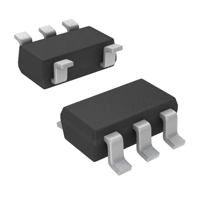
• Available Packages: SOT-23-5, MSOP-8, SOIC-8
Microchip Technology Inc.’s MCP9800/1/2/3 family of
digital temperature sensors converts temperatures
between -55°C and +125°C to a digital word. They
provide an accuracy of ±1°C (maximum) from -10°C to
+85°C.
Typical Applications:
•
•
•
•
•
•
•
Personal Computers and Servers
Hard Disk Drives and Other PC Peripherals
Entertainment Systems
Office Equipment
Data Communication Equipment
Mobile Phones
General Purpose Temperature Monitoring
VDD
PIC®
Microcontroller
GND 2
ALERT 3
5
4
R
SDA
SCLK
RPULL-UP
PIC16F737
I2C™ Port
VDD 1
This sensor has an industry standard 2-wire, I2C™/
SMBus compatible serial interface, allowing up to eight
devices to be controlled in a single serial bus. These
features make the MCP9800/1/2/3 ideal for
sophisticated
multi-zone
temperature-monitoring
applications.
Package Types
Typical Application
MCP9800/02
The
MCP9800/1/2/3
family
comes
with
user-programmable registers that provide flexibility for
temperature sensing applications. The register settings
allow user-selectable 9-bit to 12-bit temperature
measurement resolution, configuration of the
power-saving Shutdown and One-shot (single
conversion on command while in Shutdown) modes
and the specification of both temperature alert output
and hysteresis limits. When the temperature changes
beyond the specified limits, the MCP9800/1/2/3 outputs
an alert signal. The user has the option of setting the
alert output signal polarity as an active-low or
active-high comparator output for thermostat operation,
or as temperature event interrupt output for
microprocessor-based systems.
MCP9800
MCP9802
MCP9801
MCP9803
SOT-23-5
VDD 1
SOIC, MSOP
5 SDA
GND 2
ALERT 3
I/O Port
4 SCLK
SDA 1
8 VDD
SCLK 2
7 A0
ALERT 3
GND 4
6 A1
5 A2
MCP9802/03: Serial Bus time-out 35 ms (typ.)
MCP9800/01: No Serial Bus time-out
2010 Microchip Technology Inc.
DS21909D-page 1
�MCP9800/1/2/3
NOTES:
DS21909D-page 2
2010 Microchip Technology Inc.
�MCP9800/1/2/3
1.0
ELECTRICAL
CHARACTERISTICS
Absolute Maximum Ratings †
VDD....................................................................... 6.0V
†Notice: Stresses above those listed under “Maximum
ratings” may cause permanent damage to the device. This is
a stress rating only and functional operation of the device at
those or any other conditions above those indicated in the
operational listings of this specification is not implied.
Exposure to maximum rating conditions for extended periods
may affect device reliability.
Voltage at all Input/Output pins .....GND – 0.3V to 5.5V
Storage temperature .......................... -65°C to +150°C
Ambient temp. with power applied ..... -55°C to +125°C
Junction Temperature (TJ) ................................. 150°C
ESD protection on all pins (HBM:MM) .......(4 kV:400V)
Latch-Up Current at each pin ........................ ±200 mA
DC CHARACTERISTICS
Electrical Specifications: Unless otherwise indicated, VDD = 2.7V to 5.5V, GND = Ground, and
TA = -55°C to +125°C.
Parameters
Sym
Min
Typ
Max
Unit
Conditions
Operating Voltage Range
VDD
2.7
—
5.5
V
Operating Current
IDD
—
200
400
µA
Continuous Operation
Shutdown Current
ISHDN
—
0.1
1
µA
Shutdown mode
Power-on-Reset Threshold (POR)
VPOR
—
1.7
—
V
VDD falling edge
Δ°C/ΔV
—
0.2
—
°C/V
TACY
—
±0.5
—
°C
VDD = 3.3V
-10°C < TA +85°C
TACY
-1.0
—
+1.0
°C
VDD = 3.3V
-10°C < TA +125°C
TACY
-2.0
—
+2.0
°C
VDD = 3.3V
-55°C < TA +125°C
TACY
-3.0
—
+3.0
°C
VDD = 3.3V
9-bit Resolution
tCONV
—
30
75
ms
33 samples/sec (typical)
10-bit Resolution
tCONV
—
60
150
ms
17 samples/sec (typical)
11-bit Resolution
tCONV
—
120
300
ms
8 samples/sec (typical)
12-bit Resolution
tCONV
—
240
600
ms
4 samples/sec (typical)
High-level Current
IOH
—
—
1
µA
VOH = 5V
Low-level Voltage
VOL
—
—
0.4
V
IOL= 3 mA
tRES
—
1.4
—
s
Time to 63% (89°C)
27°C (Air) to 125°C (oil bath)
Power Supply
Line Regulation
VDD = 2.7V to 5.5V
Temperature Sensor Accuracy
Accuracy with 12-bit Resolution:
TA = +25°C
Internal ADC
Conversion Time:
Alert Output (Open-drain)
Thermal Response
Response Time
2010 Microchip Technology Inc.
DS21909D-page 3
�MCP9800/1/2/3
DIGITAL INPUT/OUTPUT PIN CHARACTERISTICS
Electrical Specifications: Unless otherwise indicated, VDD = 2.7V to 5.5V, GND = Ground and
TA = -55°C to +125°C.
Parameters
Sym
Min
Typ
Max
Units
Conditions
Serial Input/Output (SCLK, SDA, A0, A1, A2)
Input
High-level Voltage
VIH
0.7 VDD
—
—
V
Low-level Voltage
VIL
—
—
0.3 VDD
V
Input Current
IIN
-1
—
+1
µA
Low-level Voltage
VOL
—
—
0.4
V
IOL= 3 mA
High-level Current
IOH
—
—
1
µA
VOH = 5V
Low-level Current
IOL
6
—
—
mA
VOL = 0.6V
CIN
—
10
—
pF
VHYST
0.05 VDD
—
—
V
Output (SDA)
Capacitance
SDA and SCLK Inputs
Hysteresis
Graphical Symbol Description
INPUT
OUTPUT
Voltage
Voltage
VDD
VDD
VIH
VOL
VIL
Time
Time
Current
Current
IOL
IIN
IOH
Time
Time
TEMPERATURE CHARACTERISTICS
Electrical Specifications: Unless otherwise indicated, VDD = +2.7V to +5.5V, GND = Ground.
Parameters
Sym
Min
Typ
Max
Units
Conditions
Temperature Ranges
Specified Temperature Range
TA
-55
—
+125
°C
Operating Temperature Range
TA
-55
—
+125
°C
Storage Temperature Range
TA
-65
—
+150
°C
(Note 1)
Thermal Package Resistances
Thermal Resistance, 5L-SOT23
JA
—
256
—
°C/W
Thermal Resistance, 8L-SOIC
JA
—
163
—
°C/W
Thermal Resistance, 8L-MSOP
JA
—
206
—
°C/W
Note 1:
Operation in this range must not cause TJ to exceed Maximum Junction Temperature (+150°C).
DS21909D-page 4
2010 Microchip Technology Inc.
�MCP9800/1/2/3
SERIAL INTERFACE TIMING SPECIFICATIONS
Electrical Specifications: Unless otherwise indicated, VDD = 2.7V to 5.5V, GND = Ground, -55°C < TA < +125°C,
CL = 80 pF, and all limits measured to 50% point.
Parameters
Min
Typ
Max
Units
fSC
0
—
400
kHz
I2C MCP9800/01
fSC
10
—
400
kHz
SMBus MCP9802/03
tSC
2.5
—
—
µs
tLOW
1.3
—
—
µs
High Clock
tHIGH
0.6
—
—
µs
Rise Time
tR
20
—
300
ns
10% to 90% of VDD (SCLK, SDA)
Fall Time
tF
20
—
300
ns
90% to 10% of VDD (SCLK, SDA)
tSU-DATA
0.1
—
—
µs
Data Hold After SCLK Low
tH-DATA
0
—
0.9
µs
Start Condition Setup Time
tSU-START
0.6
—
—
µs
Start Condition Hold Time
tH-START
0.6
—
—
µs
Stop Condition Setup Time
tSU-STOP
0.6
—
—
µs
Bus Idle
tIDLE
1.3
—
—
µs
Time Out
tOUT
25
35
50
ms
2-Wire
Sym
Conditions
I2
C™/SMBus Compatible Interface
Serial Port Frequency
Clock Period
Low Clock
Data Setup Before SCLK High
MCP9802/03 only
EE
TO
-F
R
U
-S
tB
tS
W
O
tL
tH
tH
Start Condition
2010 Microchip Technology Inc.
AT
A
-D
tH
tS
U
-D
AT
A
tR
,t
F
SD
A
SC
L
tS
U
IG
H
P
-S
TA
R
T
-S
TA
R
T
Timing Diagram
Data Transmission
Stop Condition
DS21909D-page 5
�MCP9800/1/2/3
NOTES:
DS21909D-page 6
2010 Microchip Technology Inc.
�MCP9800/1/2/3
2.0
TYPICAL PERFORMANCE CURVES
Note:
The graphs and tables provided following this note are a statistical summary based on a limited number of
samples and are provided for informational purposes only. The performance characteristics listed herein
are not tested or guaranteed. In some graphs or tables, the data presented may be outside the specified
operating range (e.g., outside specified power supply range) and therefore, outside the warranted range.
Note: Unless otherwise noted: VDD = 2.7V to 5.5V.
85
105 125
Temperature Accuracy (°C)
FIGURE 2-1:
Average Temperature
Accuracy vs. Ambient Temperature, VDD = 3.3V.
2.0
1.0
400
12-Bit Resolution
160 Samples
VDD = 2.7V
VDD = 3.3V
VDD = 5.0V
VDD = 5.5V
350
-1.0
50
5
25 45
TA (°C)
65
85
Resolution
-55 -35 -15
105 125
FIGURE 2-2:
Average Temperature
Accuracy vs. Ambient Temperature.
FIGURE 2-5:
Temperature.
5
25 45
TA (°C)
65
85
105 125
Supply Current vs. Ambient
1
VDD = 3.3V
160 Samples
2.0
0.8
ISHDN (µA)
11-Bit
12-Bit
0.0
-1.0
-2.0
200
100
-3.0
1.0
VDD = 5.0V
VDD = 5.5V
250
150
-2.0
3.0
VDD = 2.7V
VDD = 3.3V
300
0.0
-55 -35 -15
Temperature Accuracy (°C)
FIGURE 2-4:
Temperature Accuracy
Histogram, TA = +25°C.
IDD (µA)
Temperature Accuracy (°C)
3.0
3.0
65
2.5
25 45
TA (°C)
2.0
5
1.5
-15
1.0
-35
0.5
-55
-3.0
Spec. Limits
-3.0
0.0
-2.0
-0.5
-1.0
-1.0
0.0
5 lots
32 Samples/lot
160 Samples
-1.5
1.0
TA = +25°C
VDD = 3.3V
-2.0
2.0
100%
90%
80%
70%
60%
50%
40%
30%
20%
10%
0%
-2.5
VDD= 3.3V
12-Bit Resolution
160 Samples
Occurrences
Temperature Accuracy (°C)
3.0
9-Bit
10-Bit
0.6
0.4
0.2
-3.0
0
-55 -35 -15
5
25 45
TA (°C)
65
85
105 125
FIGURE 2-3:
Average Temperature
Accuracy vs. Ambient Temperature, VDD = 3.3V.
2010 Microchip Technology Inc.
-55
-35 -15
5
25 45
TA (°C )
65
85
105 125
FIGURE 2-6:
Shutdown Current vs.
Ambient Temperature.
DS21909D-page 7
�MCP9800/1/2/3
Note: Unless otherwise noted: VDD = 2.7V to 5.5V.
145
VOL = 0.6V
42
VDD = 5.5V
VDD = 3.3V
VDD = 2.7V
36
30
24
18
12
105
85
65
SOIC
45
MSOP
SOT-23
25
27°C (Air) to 125°C (Oil bath)
6
-55
-35
-15
5
25 45
TA (°C)
65
85
105 125
0.4
5
-2
0
2
4
6
8
10
12
14
16
18
20
Time (s)
FIGURE 2-7:
ALERT and SDA IOL vs.
Ambient Temperature.
ALERT & SDA V OL (V)
Average of 10 samples per package
125
Temperature Data (°C)
ALERT & SDA I OL (mA)
48
FIGURE 2-9:
MCP980X Thermal
Response vs Time.
IOL = 3mA
0.3
VDD = 5.5V
VDD = 3.3V
VDD = 2.7V
0.2
0.1
0
-55 -35 -15
5
25 45
TA (°C)
65
85
105 125
FIGURE 2-8:
ALERT and SDA Output
VOL vs. Ambient Temperature.
DS21909D-page 8
2010 Microchip Technology Inc.
�MCP9800/1/2/3
3.0
PIN DESCRIPTION
The descriptions of the pins are listed in Table 3-1.
TABLE 3-1:
3.1
PIN FUNCTION TABLE
MCP9800
MCP9802
SOT-23-5
MCP9801
MCP9803
MSOP, SOIC
Symbol
5
1
SDA
4
2
SCLK
Serial Clock Input
3
3
ALERT
Temperature Alert Output
2
4
GND
5
A2
Address Select Pin (bit 2)
—
6
A1
Address Select Pin (bit 1)
—
7
A0
Address Select Pin (bit 0)
1
8
VDD
Power Supply Input
Serial Data Pin (SDA)
Serial Clock Pin (SCLK)
The SCLK is a clock input pin. All communication and
timing is relative to the signal on this pin. The clock is
generated by the host controller on the bus.
3.3
Power Supply Input (VDD)
The VDD pin is the power pin. The operating voltage, as
specified in the DC electrical specification table, is
applied on this pin.
3.4
Bidirectional Serial Data
—
The SDA is a bidirectional input/output pin, used to
serially transmit data to and from the host controller.
This pin requires a pull-up resistor to output data.
3.2
Function
Ground (GND)
The GND pin is the system ground pin.
Ground
3.5
ALERT Output
The MCP9800/1/2/3’s ALERT pin is an open-drain
output pin. The device outputs an alert signal when the
ambient
temperature
goes
beyond
the
user-programmed temperature limit.
3.6
Address Pins (A2, A1, A0)
These pins are device or slave address input pins and
are available only with the MCP9801/03. The device
addresses for the MCP9800/02 are factory-set.
The address pins are the Least Significant bits (LSb) of
the device address bits. The Most Significant bits
(MSb) (A6, A5, A4, A3) are factory-set to . This
is illustrated in Table 3-2.
TABLE 3-2:
Device
A6
A5
A4
A3
A2
A1
A0
MCP9800/02A0
1
0
0
1
0
0
0
MCP9800/02A1
1
0
0
1
0
0
1
MCP9800/02A2
1
0
0
1
0
1
0
MCP9800/02A3
1
0
0
1
0
1
1
MCP9800/02A4
1
0
0
1
1
0
0
MCP9800/02A5
1
0
0
1
1
0
1
MCP9800/02A6
1
0
0
1
1
1
0
MCP9800/02A7
1
0
0
1
1
1
1
MCP9801/03
1
0
0
1
X
X
X
Note:
2010 Microchip Technology Inc.
SLAVE ADDRESS
User-selectable address is shown by X.
DS21909D-page 9
�MCP9800/1/2/3
NOTES:
DS21909D-page 10
2010 Microchip Technology Inc.
�MCP9800/1/2/3
4.0
SERIAL COMMUNICATION
4.1.1
4.1
2-Wire SMBus/Standard Mode
I2C™ Protocol-Compatible
Interface
Data transfers are initiated by a Start condition (Start),
followed by a 7-bit device address and a read/write bit.
An Acknowledge (ACK) from the slave confirms the
reception of each byte. Each access must be
terminated by a Stop condition (Stop).
The MCP9800/1/2/3 serial clock input (SCL) and the
bidirectional serial data line (SDA) form a 2-wire
bidirectional SMBus/Standard mode I2C compatible
communication port (refer to the Digital Input/Output
Pin Characteristics Table and Serial Interface
Timing Specifications Table).
The following bus protocol has been defined:
TABLE 4-1:
Term
MCP9800 SERIAL BUS
PROTOCOL DESCRIPTIONS
Description
Master
The device that controls the serial bus,
typically a microcontroller.
Slave
The device addressed by the master,
such as the MCP9800/1/2/3.
Transmitter Device sending data to the bus.
Receiver
Device receiving data from the bus.
Start
A unique signal from master to initiate
serial interface with a slave.
Stop
A unique signal from the master to
terminate serial interface from a slave.
Read/Write A read or write to the MCP9800/1/2/3
registers.
ACK
A receiver Acknowledges (ACK) the
reception of each byte by polling the
bus.
NAK
A receiver Not-Acknowledges (NAK) or
releases the bus to show End-of-Data
(EOD).
Busy
Communication is not possible
because the bus is in use.
Not Busy
The bus is in the Idle state, both SDA
and SCL remain high.
Data Valid
SDA must remain stable before SCL
becomes high in order for a data bit to
be considered valid. During normal
data transfers, SDA only changes state
while SCL is low.
2010 Microchip Technology Inc.
DATA TRANSFER
Repeated communication is initiated after tB-FREE.
This device does not support sequential register read/
write. Each register needs to be addressed using the
Register Pointer.
This device supports the Receive Protocol. The
register can be specified using the pointer for the initial
read. Each repeated read or receive begins with a Start
condition and address byte. The MCP9800/1/2/3
retains the previously selected register. Therefore, it
outputs data from the previously-specified register
(repeated pointer specification is not necessary).
4.1.2
MASTER/SLAVE
The bus is controlled by a master device (typically a
microcontroller) that controls the bus access and
generates the Start and Stop conditions. The
MCP9800/1/2/3 is a slave device and does not control
other devices in the bus. Both master and slave
devices can operate as either transmitter or receiver.
However, the master device determines which mode is
activated.
4.1.3
START/STOP CONDITION
A high-to-low transition of the SDA line (while SCL is
high) is the Start condition. All data transfers must be
preceded by a Start condition from the master. If a Start
condition is generated during data transfer, the
MCP9800/1/2/3 resets and accepts the new Start
condition.
A low-to-high transition of the SDA line (while SCL is
high) signifies a Stop condition. If a Stop condition is
introduced during data transmission, the MCP9800/1/
2/3 releases the bus. All data transfers are ended by a
Stop condition from the master.
4.1.4
ADDRESS BYTE
Following the Start condition, the host must transmit an
8-bit address byte to the MCP9800/1/2/3. The address
for
the
MCP9800
Temperature
Sensor
is
‘1001,A2,A1,A0’ in binary, where the A2, A1 and A0
bits are set externally by connecting the corresponding
pins to VDD ‘1’ or GND ‘0’. The 7-bit address
transmitted in the serial bit stream must match the
selected address for the MCP9800/1/2/3 to respond
with an ACK. Bit 8 in the address byte is a read/write
bit. Setting this bit to ‘1’ commands a read operation,
while ‘0’ commands a write operation (see Figure 4-1).
DS21909D-page 11
�MCP9800/1/2/3
4.1.6
Address Byte
1
SCL
2
1
SDA
0
3
4
5
6
7
8
A
C
K
1 A2 A1 A0
0
9
Start
Address
Code
Slave
Address
R/W
PIC18FXXXX Response
FIGURE 4-1:
4.1.5
Device Addressing.
DATA VALID
After the Start condition, each bit of data in
transmission needs to be settled for a time specified by
tSU-DATA before SCL toggles from low-to-high (see
“Serial Interface Timing Specifications” on Page 5).
DS21909D-page 12
ACKNOWLEDGE (ACK)
Each receiving device, when addressed, is obliged to
generate an ACK bit after the reception of each byte.
The master device must generate an extra clock pulse
for ACK to be recognized.
The acknowledging device pulls down the SDA line for
tSU-DATA before the low-to-high transition of SCL from
the master. SDA also needs to remain pulled down for
tH-DATA after a high-to-low transition of SCL.
During read, the master must signal an End-of-Data
(EOD) to the slave by not generating an ACK bit (NAK)
once the last bit has been clocked out of the slave. In
this case, the slave will leave the data line released to
enable the master to generate the Stop condition.
2010 Microchip Technology Inc.
�MCP9800/1/2/3
5.0
FUNCTIONAL DESCRIPTION
The MCP9800/1/2/3 temperature sensor consists of a
band-gap type temperature sensor, a Analog-toDigital Converter (ADC), user-programmable registers
and a 2-wire I2C protocol-compatible serial interface.
Resolution
5.1
Temperature Sensor
The MCP9800/1/2/3 uses the difference in the baseemitter voltage of a transistor while its collector current
is changed from IC1 to IC2. With this method, the VBE
depends only on the ratio of the two currents and the
ambient temperature, as shown in Equation 5-1.
EQUATION 5-1:
One-Shot
Shutdown
Fault Queue
Alert Polarity
kT
0.5°C
0.25°C
0.125°C
0.0625°C
V BE = ------ ln IC 1 IC 2
q
Where:
T = temperature in kelvin
VBE = change in diode base-emitter
voltage
Alert Comp/Int
k = Boltzmann's constant
Configuration
Register
Temperature
Register
THYST
Register
Band-Gap
Temperature
Sensor
TSET
Register
Register
Pointer
FIGURE 5-1:
q = electron charge
ADC
I2C™
Interface
Functional Block Diagram.
2010 Microchip Technology Inc.
IC1 and IC2 = currents with n:1 ratio
5.2
Analog-to-Digital Converter
A Sigma-Delta ADC is used to convert VBE to a digital
word that corresponds to the transistor temperature.
The converter has an adjustable resolution from 0.5°C
(at 30 ms conversion time) to 0.0625°C (at 240 ms
conversion time). Thus, it allows the user to make
trade-offs between resolution and conversion time.
Refer to Section 5.3.2 “Sensor Configuration
Register (CONFIG)” and Section 5.3.4.7 “ ADC
Resolution” for details.
DS21909D-page 13
�MCP9800/1/2/3
5.3
Registers
Resolution
The MCP9800/1/2/3 has four registers that are
user-accessible. These registers are specified as the
Ambient Temperature (TA) register, the Temperature
Limit-set (TSET) register, the Temperature Hysteresis
(THYST) register and device Configuration (CONFIG)
register.
One-Shot
Shutdown
Fault Queue
The Ambient Temperature register is a read-only
register and is used to access the ambient temperature
data. The data from the ADC is loaded in parallel in the
register. The Temperature Limit-set and Temperature
Hysteresis registers are read/write registers that
provide user-programmable temperature limits. If the
ambient temperature drifts beyond the programmed
limits, the MCP9800/1/2/3 outputs an alert signal using
the ALERT pin (refer to Section 5.3.4.3 “ALERT
Output Configuration”). The device Configuration
register provides access for the user to configure the
MCP9800/1/2/3’s various features. These registers are
described in further detail in the following sections.
Alert Polarity
Alert Comp/Int
Configuration
Register
THYST
Register
ALERT Output
Control Logic
TSET
Register
The registers are accessed by sending Register Pointers to the MCP9800/1/2/3 using the serial interface.
This is an 8-bit pointer. However, the two Least
Significant bits (LSbs) are used as pointers and all
other bits need to be cleared . This device has additional registers that are reserved for test and
calibration. If these registers are accessed, the device
may not perform according to the specification. The
pointer description is shown below.
REGISTER 5-1:
ALERT
Output
Temperature
Register
FIGURE 5-2:
Register Block Diagram.
REGISTER POINTER
U-0
U-0
U-0
U-0
U-0
U-0
R/W-0
R/W-0
0
0
0
0
0
0
P1
P0
bit 7
bit 0
Legend:
R = Readable bit
W = Writable bit
U = Unimplemented bit, read as ‘0’
-n = Value at POR
‘1’ = Bit is set
‘0’ = Bit is cleared
bit 7-2
Unimplemented: Read as ‘0’
bit 1-0
Px: Pointer bits
00 = Temperature register (TA)
01 = Configuration register (CONFIG)
10 = Temperature Hysteresis register (THYST)
11 = Temperature Limit-set register (TSET)
x = Bit is unknown
.
DS21909D-page 14
2010 Microchip Technology Inc.
�MCP9800/1/2/3
TABLE 5-1:
Register
Pointer
P1 P0
MSB/
LSB
BIT ASSIGNMENT SUMMARY FOR ALL REGISTERS
Bit Assignment
7
Ambient Temperature Register (TA)
0 0
6
5
4
3
2
1
0
23°C
22°C
21°C
20°C
0
0
0
0
ALERT
Polarity
COMP/INT
Shutdown
MSB
Sign
26°C
25°C
24°C
LSB
2-1°C
2-2°C
2-3°C
2-4°C
Sensor Configuration Register (CONFIG)
0 1
LSB
One-Shot
Resolution
Fault Queue
Temperature Hysteresis Register (THYST)
1 0
MSB
Sign
26°C
25°C
24°C
23°C
22°C
21°C
20°C
LSB
2-1°C
0
0
0
0
0
0
0
Temperature Limit-Set Register (TSET)
1 1
MSB
Sign
26°C
25°C
24°C
23°C
22°C
21°C
20°C
LSB
2-1°C
0
0
0
0
0
0
0
2010 Microchip Technology Inc.
DS21909D-page 15
�MCP9800/1/2/3
5.3.1
AMBIENT TEMPERATURE
REGISTER (TA)
EQUATION 5-2:
The MCP9800/1/2/3 has a 16-bit read-only Ambient
Temperature register that contains 9-bit to 12-bit
temperature data. (0.5°C to 0.0625°C resolutions,
respectively). This data is formatted in two’s
complement. The bit assignments, as well as the
corresponding resolution, is shown in the register
assignment below.
T A = Code 2
–4
Where:
TA = Ambient Temperature (°C)
Code = MCP9800 output in decimal
The refresh rate of this register depends on the
selected ADC resolution. It takes 30 ms (typical) for
9-bit data and 240 ms (typical) for 12-bit data. Since
this register is double-buffered, the user can read the
register
while
the
MCP9800/1/2/3
performs
Analog-to-Digital conversion in the background. The
decimal code to ambient temperature conversion is
shown in Equation 5-2:
REGISTER 5-2:
AMBIENT TEMPERATURE REGISTER (TA) – ADDRESS b
Upper Half:
R-0
R-0
R-0
R-0
R-0
R-0
R-0
R-0
Sign
26 °C
25 °C
24 °C
23 °C
22 °C
21 °C
20 °C
bit 15
bit 8
Lower Half:
R-0
2
-1 °C/bit
R-0
R-0
R-0
R-0
R-0
R-0
R-0
2-2 °C
2-3 °C
2-4 °C
0
0
0
0
bit 7
bit 0
Legend:
R = Readable bit
W = Writable bit
U = Unimplemented bit, read as ‘0’
-n = Value at POR
‘1’ = Bit is set
‘0’ = Bit is cleared
Note 1:
x = Bit is unknown
When the 0.5°C, 0.25°C or 0.125°C resolutions are selected, bit 6, bit 7 or bit 8 will remain clear ,
respectively.
DS21909D-page 16
2010 Microchip Technology Inc.
�MCP9800/1/2/3
1
2
3
4
5
6
7
8
1
2
3
4
5
6
7
8
Note:
SCL
SDA
S
1
0
0
A
2
1
A
1
A
A
0
W C
K
0
0
0
Address Byte
0
0
0
0
It is not necessary to
select the Register
Pointer if it was set
from the previous read/
write.
(see Section 4.1.1)
A
C
K
0
TA Pointer
PIC18FXXX
PIC18FXXX
1
2
3
4
5
6
7
8
1
0
0
1
A
2
A
1
A
0
R C
1
2
3
4
5
6
7
8
0
0
0
1
1
0
0
1
1
2
3
4
5
6
7
8
0
1
0
0
0
0
0
0
SCL
SDA
S
A
K
Address Byte
A
C
K
P
LSB Data
MSB Data
PIC18FXXX
N
A
K
Master
Master
FIGURE 5-3:
Timing Diagram for Reading +25.25°C Temperature from the TA Register (See
Section 5.3.1 “Ambient Temperature Register (TA)”).
2010 Microchip Technology Inc.
DS21909D-page 17
�MCP9800/1/2/3
5.3.2
SENSOR CONFIGURATION
REGISTER (CONFIG)
The MCP9800/1/2/3 has an 8-bit read/write
Configuration register that allows the user to select the
different features. These features include shutdown,
ALERT output select as comparator or interrupt output,
ALERT output polarity, fault queue cycle, temperature
measurement resolution and One-shot mode (single
conversion while in shutdown). These functions are
described in detail in the following sections.
REGISTER 5-3:
R/W-0
CONFIGURATION REGISTER (CONFIG) – ADDRESS b
R/W-0
One-Shot
R/W-0
R/W-0
Resolution
R/W-0
Fault Queue
R/W-0
R/W-0
R/W-0
ALERT
Polarity
COMP/INT
Shutdown
bit 7
bit 0
Legend:
R = Readable bit
W = Writable bit
U = Unimplemented bit, read as ‘0’
-n = Value at POR
‘1’ = Bit is set
‘0’ = Bit is cleared
bit 7
ONE-SHOT bit
1 = Enabled
0 = Disabled (Power-up default)
bit 5-6
ADC RESOLUTION bits
00 = 9 bit or 0.5°C (Power-up default)
01 = 10 bit or 0.25°C
10 = 11 bit or 0.125°C
11 = 12 bit or 0.0625°C
bit 3-4
FAULT QUEUE bits
00 = 1 (Power-up default)
01 = 2
10 = 4
11 = 6
bit 2
ALERT POLARITY bit
1 = Active-high
0 = Active-low (Power-up default)
bit 1
COMP/INT bit
1 = Interrupt mode
0 = Comparator mode (Power-up default)
bit 0
SHUTDOWN bit
1 = Enable
0 = Disable (Power-up default)
DS21909D-page 18
x = Bit is unknown
2010 Microchip Technology Inc.
�MCP9800/1/2/3
• Writing to the CONFIG Register to change the resolution to 0.0625°C b.
1
2
3
4
5
6
7
8
1
0
0
1
A
2
A
1
A
0
W C
1
2
3
4
5
6
7
8
0
0
0
0
0
0
0
1
SCL
SDA
S
A
K
Address Byte
A
C
K
CONFIG Pointer
PIC18FXXX
PIC18FXXX
1
2
3
4
5
6
7
8
0
1
1
0
0
0
0
0
1
A
C
K
P
MSB Data
PIC18FXXX
• Reading the CONFIG Register.
1
2
3
4
5
6
7
8
1
2
3
4
5
6
7
8
Note:
SCL
SDA
S
1
0
0
A
2
1
A
1
A
A
0
W C
K
0
0
Address Byte
0
0
0
0
0
A
C
K
1
It is not necessary to
select the Register
Pointer if it was set
from the previous read/
write
(see Section 4.1.1).
CONFIG Pointer
PIC18FXXX
PIC18FXXX
1
2
3
4
5
6
7
8
1
0
0
1
A
2
A
1
A
0
R C
1
2
3
4
5
6
7
8
0
1
1
0
0
0
0
0
SCL
SDA
S
A
K
Address Byte
N
A
K
P
Data
PIC18FXXX
FIGURE 5-4:
Timing Diagram for Writing and Reading from the Configuration Register (See
Section 5.3.2 “Sensor Configuration Register (CONFIG)”).
2010 Microchip Technology Inc.
DS21909D-page 19
�MCP9800/1/2/3
5.3.3
TEMPERATURE HYSTERESIS
REGISTER (THYST)
The MCP9800/1/2/3 has a 16-bit read/write
Temperature Hysteresis register that contains a 9-bit
data in two’s compliment format. This register is used
to set a hysteresis for the TSET limit. Therefore, the data
represents a minimum temperature limit. If the ambient
temperature drifts below the specified limit, the
MCP9800/1/2/3 asserts an alert output (refer to
Section 5.3.4.3 “ALERT Output Configuration”).
This register uses the nine Most Significant bits (MSbs)
and all other bits are “don’t cares”.
The power-up default value of THYST register is 75°C,
or b in binary.
REGISTER 5-4:
TEMPERATURE HYSTERESIS REGISTER (THYST) – ADDRESS b
Upper Half:
R/W-0
Sign
R/W-1
R/W-0
R/W-0
R/W-1
R/W-0
R/W-1
R/W-1
6 °C
25 °C
24 °C
23 °C
22 °C
21 °C
20 °C
2
bit 15
bit 8
Lower Half:
R/W-0
R-0
R-0
R-0
R-0
R-0
R-0
R-0
2-1 °C
0
0
0
0
0
0
0
bit 7
bit 0
Legend:
R = Readable bit
W = Writable bit
U = Unimplemented bit, read as ‘0’
-n = Value at POR
‘1’ = Bit is set
‘0’ = Bit is cleared
DS21909D-page 20
x = Bit is unknown
2010 Microchip Technology Inc.
�MCP9800/1/2/3
• Writing to the THYST Register to set the temperature hysteresis to 95°C b.
1
2
3
4
5
6
7
8
1
0
0
1
A
2
A
1
A
0
W C
1
2
3
4
5
6
7
8
0
0
0
0
0
0
1
0
SCL
SDA
S
A
K
Address Byte
A
C
K
THYST Pointer
PIC18FXXX
PIC18FXXX
1
2
3
4
5
6
7
8
0
1
0
1
1
1
1
1
A
C
K
1
2
3
4
5
6
7
8
0
0
0
0
0
0
0
0
MSB Data
A
C
K
P
LSB Data
PIC18FXX
PIC18FXXX
• Reading the THYST Register.
1
2
3
4
5
6
7
8
1
2
3
4
5
6
7
8
Note:
SCL
SDA
S
1
0
0
A
2
1
A
1
A
A
0
W C
K
0
0
Address Byte
0
0
0
0
1
It is not necessary to
select the Register
Pointer if it was set
from the previous read/
write
(see Section 4.1.1).
A
C
K
0
THYST Pointer
PIC18FXXX
PIC18FXXX
1
2
3
4
5
6
7
8
1
0
0
1
A
2
A
1
A
0
R C
1
2
3
4
5
6
7
8
0
1
0
1
1
1
1
1
1
2
3
4
5
6
7
8
0
0
0
0
0
0
0
0
SCL
SDA
S
A
K
Address Byte
A
C
K
P
LSB Data
MSB Data
PIC18FXXX
N
A
K
Master
Master
FIGURE 5-5:
Timing Diagram for Writing and Reading from the Temperature Hysteresis Register
(See Section 5.3.3 “Temperature Hysteresis Register (THYST)”).
2010 Microchip Technology Inc.
DS21909D-page 21
�MCP9800/1/2/3
5.3.4
TEMPERATURE LIMIT-SET
REGISTER (TSET)
The MCP9800/1/2/3 has a 16-bit read/write
Temperature Limit-Set register (TSET) which contains a
9-bit data in two’s compliment format. This data
represents a maximum temperature limit. If the ambient
temperature exceeds this specified limit, the
MCP9800/1/2/3 asserts an alert output. (Refer to
Section 5.3.4.3 “ALERT Output Configuration”).
This register uses the nine Most Significant bits (MSbs)
and all other bits are “don’t cares”.
The power-up default value of the TSET register is
80°C, or b in binary.
REGISTER 5-5:
TEMPERATURE LIMIT-SET REGISTER (TSET) – ADDRESS b
Upper Half:
R/W-0
R/W-1
R/W-0
R/W-1
R/W-0
R/W-0
R/W-0
R/W-0
Sign
26 °C
25 °C
24 °C
23 °C
22 °C
21 °C
20 °C
bit 15
bit 8
Lower Half:
R/W-0
2
-1 °C
R-0
R-0
R-0
R-0
R-0
R-0
R-0
0
0
0
0
0
0
0
bit 7
bit 0
Legend:
R = Readable bit
W = Writable bit
U = Unimplemented bit, read as ‘0’
-n = Value at POR
‘1’ = Bit is set
‘0’ = Bit is cleared
DS21909D-page 22
x = Bit is unknown
2010 Microchip Technology Inc.
�MCP9800/1/2/3
• Writing to the TSET Register to set the temperature limit to 90°C, b
1
2
3
4
5
6
7
8
1
0
0
1
A
2
A
1
A
0
W C
1
2
3
4
5
6
7
8
0
0
0
0
0
0
1
1
SCL
SDA
S
A
K
Address Byte
A
C
K
TSET Pointer
PIC18FXXX
PIC18FXXX
1
2
3
4
5
6
7
8
0
1
0
1
1
0
1
0
A
C
K
1
2
3
4
5
6
7
8
0
0
0
0
0
0
0
0
MSB Data
A
C
K
P
LSB Data
PIC18FXX
PIC18FXXX
• Reading the TSET Register.
1
2
3
4
5
6
7
8
1
2
3
4
5
6
7
8
Note:
SCL
SDA
S
1
0
0
A
2
1
A
1
A
A
0
W C
K
0
0
0
Address Byte
0
0
0
1
It is not necessary to
select the Register
Pointer if it was set
from the previous read/
write.
(see Section 4.1.1)
A
C
K
1
TSET Pointer
PIC18FXXX
PIC18FXXX
1
2
3
4
5
6
7
8
1
0
0
1
A
2
A
1
A
0
R C
1
2
3
4
5
6
7
8
0
1
0
1
1
0
1
0
1
2
3
4
5
6
7
8
0
0
0
0
0
0
0
0
SCL
SDA
S
A
K
Address Byte
A
C
K
P
LSB Data
MSB Data
PIC18FXXX
N
A
K
Master
Master
FIGURE 5-6:
Timing Diagram for Writing and Reading from the Temperature Limit-set Register
(See Section 5.3.4 “Temperature Limit-Set Register (TSET)”).
2010 Microchip Technology Inc.
DS21909D-page 23
�MCP9800/1/2/3
5.3.4.1
5.3.4.3
Shutdown Mode
The Shutdown mode disables all power-consuming
activities (including temperature sampling operations)
while leaving the serial interface active. The device
consumes 2 µA (maximum) in this mode. It remains in
this mode until the Configuration register is updated to
enable continuous conversion or until power is
recycled.
In Shutdown mode, the CONFIG, TA, TSET and THYST
registers can be read or written to; however, the serial
bus activity will increase the shutdown current.
5.3.4.2
One-Shot Mode
The MCP9800/1/2/3 can also be used in a One-shot
mode that can be selected using bit 7 of the CONFIG
register. The One-shot mode performs a single
temperature measurement and returns to Shutdown
mode. This mode is especially useful for low-power
applications where temperature is measured upon
command from a controller. For example, a 9-bit TA in
One-shot mode consumes 200 µA (typical) for 30 ms
and 0.1 µA (typical) during shutdown.
To access this feature, the device needs to initially be
in Shutdown mode. This is done by sending a byte to
the CONFIG register with bit 0 set and bit 7 cleared
. Once the device is in Shutdown mode, the
CONFIG register needs to be written to again, with bit
0 and bit 7 set . This begins the single conversion
cycle of tCONV, 30ms for 9-bit data. Once the
conversion is completed, TA is updated and bit 7 of
CONFIG becomes cleared by the MCP9800/1/2/3.
TABLE 5-2:
SHUTDOWN AND ONE-SHOT
MODE DESCRIPTION
Operational Mode
One-Shot
(Bit 7)
Shutdown
(Bit 0)
Continuous Conversion
0
0
Shutdown
0
1
Continuous Conversion
1
0
(One-shot is ignored)
One-shot (Note 1)
1
1
Note 1: The shutdown command needs to
be programmed before sending a
one-shot command .
ALERT Output Configuration
The ALERT output can be configured as either a
comparator output or as Interrupt Output mode using
bit 1 of CONFIG. The polarity can also be specified as
an active-high or active-low using bit 2 of CONFIG. The
following sections describe each output mode, while
Figure 5-7 gives a graphical description.
5.3.4.4
Comparator Mode
In Comparator mode, the ALERT output is asserted
when TA is greater than TSET. The pin remains active
until TA is lower than THYST. The Comparator mode is
useful for thermostat-type applications, such as turning
on a cooling fan or triggering a system shutdown when
the temperature exceeds a safe operating range.
In Comparator mode, if the device enters the Shutdown
mode with asserted ALERT output, the output remains
active during shutdown. The device must be operating
in continuous conversion, with TA below THYST, for the
ALERT output to be deasserted.
5.3.4.5
Interrupt Mode
In Interrupt mode, the ALERT output is asserted when
TA is greater than TSET. However, the output is
deasserted when the user performs a read from any
register. This mode is designed for interrupt-driven,
microcontroller-based systems. The microcontroller
receiving the interrupt will have to acknowledge the
interrupt by reading any register from the MCP9800/1/
2/3. This will clear the interrupt and the ALERT pin will
become deasserted. When TA drifts below THYST, the
MCP9800/1/2/3 outputs another interrupt and the
controller needs to read a register to deassert the
ALERT output. Shutting down the device will also reset,
or deassert, the ALERT output.
TSET
TA
THYST
ALERT
Comparator mode
Active-low
ALERT
Interrupt mode
Active-low
Register
Read
*
* See Section 5.3.4.5 “Interrupt Mode”
FIGURE 5-7:
DS21909D-page 24
Alert Output.
2010 Microchip Technology Inc.
�MCP9800/1/2/3
5.3.4.6
5.4
Fault Queue
The fault queue feature can be used as a filter to lessen
the probability of spurious activation of the ALERT pin.
TA must remain above TSET for the consecutive
number of conversion cycles selected using the Fault
Queue bits. Bit 3 and bit 4 of CONFIG can be used to
select up to six fault queue cycles. For example, if six
fault queues are selected, TA must be greater than
TSET for six consecutive conversions before ALERT is
asserted as a comparator or an interrupt output.
This queue setting also applies for THYST. If six fault
queues are selected, TA must remain below THYST for
six consecutive conversions before ALERT is
deasserted (Comparator mode) or before another
interrupt is asserted (Interrupt mode).
5.3.4.7
The MCP9800/1/2/3 has an internal Power-on Reset
(POR) circuit. If the power supply voltage VDD glitches
down to the 1.7V (typical) threshold, the device resets
the registers to the power-up default settings.
Table 5-4 shows the power-up default summary.
TABLE 5-4:
POWER-UP DEFAULTS
Register
Data
(Hex)
TA
TSET
THYST
Pointer
0000
A000
9600
00
CONFIG
00
ADC Resolution
The MCP9800/1/2/3 provides access to select the ADC
resolution from 9-bit to 12-bit (0.5°C to 0.0625°C
resolution) using bit 6 and bit 5 of the CONFIG register.
The user can gain better insight into the trends and
characteristics of the ambient temperature by using a
finer resolution. Increasing the resolution also reduces
the quantization error. Figure 2-3 shows accuracy
versus resolution.
Table 5-3 shows the TA register conversion time for the
corresponding resolution.
TABLE 5-3:
Summary of Power-up Condition
Power-up Defaults
0°C
80°C
75°C
Temperature register
Continuous Conversion
Comparator mode
Active-low Output
Fault Queue 1
9-bit Resolution
At power-up, the MCP9800/1/2/3 has an inherent 2 ms
(typical) power-up delay before updating the registers
with default values and start a conversion cycle. This
delay reduces register corruption due to unsettled
power. After power-up, it takes tCONV for the TCN75A
to update the TA register with valid temperature data.
RESOLUTION AND
CONVERSION TIME
Bits
Resolution
tCONV (typical)
9
10
11
12
0.5
0.25
0.125
0.0625
30 ms
60 ms
120 ms
240 ms
2010 Microchip Technology Inc.
DS21909D-page 25
�MCP9800/1/2/3
NOTES:
DS21909D-page 26
2010 Microchip Technology Inc.
�MCP9800/1/2/3
6.0
APPLICATIONS INFORMATION
6.1
Connecting to the Serial Bus
The SDA and SCL serial interface are open-drain pins
that require pull-up resistors. This configuration is
shown in Figure 6-1.
VDD
R
R
SDA
SCL
PIC®
MCU
FIGURE 6-1:
Interface.
MCP9800/1/2/3
Pull-up Resistors on Serial
The MCP9800/1/2/3 is designed to meet 0.4V
(maximum) voltage drop at 3 mA of current. This allows
the MCP9800/1/2/3 to drive lower values of pull-up
resistors and higher bus capacitance. In this
application, all devices on the bus must meet the same
pull-down current requirements.
6.2
The ALERT output can be wired with a number of other
open-drain devices. In such applications, the output
needs to be programmed as an active-low output. Most
systems will require pull-up resistors for this
configuration.
6.3
The MCP9800/1/2/3 does not require any additional
components besides the master controller in order to
measure temperature. However, it is recommended
that a decoupling capacitor of 0.1 µF to 1 µF be used
between the VDD and GND pins. A high-frequency
ceramic capacitor is recommended. It is necessary for
the capacitor to be located as close as possible to the
power pins in order to provide effective noise
protection.
For applications where a switching regulator is used to
power the sensor, it is recommended to add a 200Ω
resistor in series to VDD to filter out the switcher noise
from the sensor. It is also recommended to add the
series resistor in applications where a linear regulator
is used to step-down a switching regulator voltage to
power the sensor. For example, if a linearly regulated
3.3V from a 5V switching regulator is used to power the
sensor, add a 200Ω series resistor (refer to Figure 6-3).
MCP9800/1/2/3
Typical Application
Microchip provides several microcontroller product
lines with Master Synchronous Serial Port modules
(MSSP) that include the I2C interface mode. This
module implements all master and slave functions and
simplifies the firmware development overhead.
Figure 6-2 shows a typical application using the
PIC16F737 as a master to control other Microchip
slave products, such as EEPROM, fan speed
controllers and the MCP9800 temperature sensor
connected to the bus.
PIC16F737
Microcontroller
24LC01
EEPROM
TC654
Fan Speed
Controller
TCN75A
Temperature
Sensor
FIGURE 6-2:
Bus.
Multiple Devices on I2C™
2010 Microchip Technology Inc.
200
Switching
Regulator
VDD
0.1 µF
bypass
MCP9800/1/2/3
Switching
Regulator
Linear
Regulator
FIGURE 6-3:
Single Resistor.
6.4
SDA SCL
Layout Considerations
200
VDD
0.1 µF
bypass
Power-supply Filter Using a
Thermal Considerations
The MCP9800/1/2/3 measures temperature by
monitoring the voltage of a diode located in the die. A
low-impedance thermal path between the die and the
Printed Circuit Board (PCB) is provided by the pins.
Therefore, the MCP9800/1/2/3 effectively monitors the
temperature of the PCB. However, the thermal path for
the ambient air is not as efficient because the plastic
device package functions as a thermal insulator.
A potential for self-heating errors can exist if the
MCP9800/1/2/3 SDA and SCL communication lines
are heavily loaded with pull-ups. Typically, the
self-heating error is negligible because of the relatively
small current consumption of the MCP9800/1/2/3.
However, in order to maximize the temperature
accuracy, the SDA and SCL pins need to be lightly
loaded.
DS21909D-page 27
�MCP9800/1/2/3
NOTES:
DS21909D-page 28
2010 Microchip Technology Inc.
�MCP9800/1/2/3
7.0
PACKAGING INFORMATION
7.1
Package Marking Information
5-Lead SOT-23
Example:
XXNN
Part Number
LDNN
MCP9802A0T-M/OT
JKNN
LENN
MCP9802A1T-M/OT
JLNN
MCP9800A2T-M/OT
LFNN
MCP9802A2T-M/OT
JMNN
MCP9800A3T-M/OT
LGNN
MCP9802A3T-M/OT
JPNN
MCP9800A4T-M/OT
LHNN
MCP9802A4T-M/OT
JQNN
MCP9800A5T-M/OT
LJNN
MCP9802A5T-M/OT
JRNN
MCP9800A6T-M/OT
LKNN
MCP9802A6T-M/OT
JSNN
MCP9800A7T-M/OT
LLNN
MCP9802A7T-M/OT
JTNN
Example:
9803M
044256
8-Lead SOIC (150 mil)
e3
*
Note:
MCP9802
MCP9800A1T-M/OT
XXXXX
YWWNNN
Legend: XX...X
Y
YY
WW
NNN
Part Number
MCP9800A0T-M/OT
8-Lead MSOP
XXXXXXXX
XXXXYYWW
NNN
MCP9800
Example:
MCP9803
SN1044
256
Customer-specific information
Year code (last digit of calendar year)
Year code (last 2 digits of calendar year)
Week code (week of January 1 is week ‘01’)
Alphanumeric traceability code
Pb-free JEDEC designator for Matte Tin (Sn)
This package is Pb-free. The Pb-free JEDEC designator ( e3 )
can be found on the outer packaging for this package.
In the event the full Microchip part number cannot be marked on one line, it will
be carried over to the next line, thus limiting the number of available
characters for customer-specific information.
2010 Microchip Technology Inc.
DS21909D-page 29
�MCP9800/1/2/3
�������
���
�����
����
��������
������������������
�����
.���#�
��� #��$��
�#�
��/��
�!��-��� 0�
�
�
�
�#�
���������
�1��/�������
��%���#��������#
!��#�
�##
+22---���������
����2
��/�����
b
N
E
E1
3
2
1
e
e1
D
A2
A
c
φ
A1
L
L1
3��#
���
� ����4���#
5$�8
���%�1��
��44��"�"��
��5
56�
��7
5
(
4
�!�1�#��
���(�)�*
6$# �!
�4
�!�1�#��
�
6,
�����9
���#
�
����
:
���!
!�1��/��
�����/�
��
��;�
:
����
�#��!�%%
��
����
:
���(
6,
�����
:
��>
4
�!�����/�
�
���;
:
���=
4
�!�