MCP98242
Memory Module Temperature Sensor w/EEPROM for SPD
Features:
Description:
•
•
•
•
•
•
Microchip Technology Inc.’s MCP98242 digital
temperature sensor converts temperature from -40°C
and +125°C to a digital word. This sensor meets
JEDEC Specification JC42.4 Mobile Platform Memory
Module Thermal Sensor Component. It provides an
accuracy of ±0.5°C/±1°C (typical/maximum) from
+75°C to +95°C. In addition, this device has an internal
256 Byte EEPROM which can be used to store memory
module and vendor information.
Temperature Sensor + 256 Byte Serial EEPROM
EEPROM for Serial Presence Detect (SPD)
Optimized for Voltage Range: 3.0V to 3.6V
Shutdown/Standby Current: 3 µA (maximum)
2-wire Interface: I2C™/SMBus Compatible
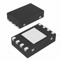
Available Packages: DFN-8, TDFN-8, UDFN-8,
TSSOP-8
Temperature Sensor Features:
• Temperature-to-Digital Converter
• Operating Current: 200 µA (typical)
• Accuracy:
- ±0.5°C/±1°C (typ./max.) +75°C to +95°C
- ±1°C/±2°C (typ./max.) +40°C to +125°C
- ±2°C/±3°C (typ./max.) -20°C to +125°C
Serial EEPROM Features:
• Operating Current:
- Write 1.1 mA (typical) for 3.5 ms (typical)
- Read 100 µA (typical)
• Permanent and Reversible Software Write-Protect
• Software Write Protection for the Lower 128 Bytes
• Organized as 1 Block of 256 Bytes (256x8)
Typical Applications:
• DIMM Modules
• Laptops, Personal Computers and Servers
• Hard Disk Drives and Other PC Peripherals
The MCP98242 digital temperature sensor comes with
user-programmable registers that provide flexibility for
DIMM temperature-sensing applications. The registers
allow user-selectable settings such as Shutdown or
Low-Power modes and the specification of
temperature event and critical output boundaries.
When the temperature changes beyond the specified
boundary limits, the MCP98242 outputs an Event
signal. The user has the option of setting the Event
output signal polarity as either an active-low or
active-high comparator output for thermostat operation,
or as a temperature event interrupt output for
microprocessor-based systems. The Event output can
also be configured as a critical temperature output.
The EEPROM is designed specifically for DRAM
DIMMs (Dual In-line Memory Modules) Serial Presence
Detect (SPD). The lower 128 bytes (address 00h to
7Fh) can be Permanent Write-Protected (PWP) or
Software Reversible Write-Protected (SWP). This
allows DRAM vendor and product information to be
stored and write-protected. The upper 128 bytes
(address 80h to FFh) can be used for general purpose
data storage. These addresses are not write-protected.
This sensor has an industry standard 2-wire, I2C/
SMBus compatible serial interface, allowing up to eight
devices to be controlled in a single serial bus. To
maintain interchangeability with the I2C/SMBus
interface the electrical specifications are specified with
the operating voltage of 3.0V to 3.6V. In addition, a
40 ms (typical) time out is implemented.
DIMM MODULE
Memory
MCP98242
Temperature Sensor + EEPROM
• ±0.5°C (typ.) Sensor
• 256 Byte EEPROM for SPD
Package Types
MCP98242
8-Pin DFN/TDFN/UDFN (2x3) * 8-Pin TSSOP
SDA
SCL
Event
8 VDD
8 VDD
A1 2
7 Event A1 2
6 SCLK A2 3
7 Event
5 SDA GND 4
5 SDA
A2 3
3.3VDD_SPD
A0 1
A0 1
GND 4
EP
9
6 SCLK
* Includes Exposed Thermal Pad (EP); see Table 3-1.
2010 Microchip Technology Inc.
DS21996D-page 1
�MCP98242
Notes:
DS21996D-page 2
2010 Microchip Technology Inc.
�MCP98242
1.0
ELECTRICAL
CHARACTERISTICS
†Notice: Stresses above those listed under “Maximum
ratings” may cause permanent damage to the device. This is
a stress rating only and functional operation of the device at
those or any other conditions above those indicated in the
operational listings of this specification is not implied.
Exposure to maximum rating conditions for extended periods
may affect device reliability.
Absolute Maximum Ratings †
VDD.................................................................................. 6.0V
Voltage at all Input/Output pins ............... GND – 0.3V to 6.0V
Pin A0 ................................................... GND – 0.3V to 12.5V
Storage temperature .....................................-65°C to +150°C
Ambient temp. with power applied ................-40°C to +125°C
Junction Temperature (TJ) .......................................... +150°C
ESD protection on all pins (HBM:MM) ................. (4 kV:300V)
Latch-Up Current at each pin (+25°C) ..................... ±200 mA
DC CHARACTERISTICS
Electrical Specifications: Unless otherwise indicated, VDD = 3.0V to 3.6V, GND = Ground, SDA/SCL pulled-up to
VDD, and TA = -20°C to +125°C.
Parameters
Sym
Min
Typ
Max
Unit
Conditions
VDD
3.0
—
3.6
V
Temperature Sensor
IDD
—
200
500
µA
EEPROM Inactive
EEPROM write
IDD
—
1100
2000
µA
Sensor in Shutdown mode (for tWC)
Power Supply
Operating Voltage
Operating Current
IDD
—
100
500
µA
Sensor in Shutdown mode
Shutdown Current
EEPROM read
ISHDN
—
1
3
µA
EEPROM Inactive,
Sensor in Shutdown mode
Power-on-Reset (POR)
Threshold
VPOR
—
2.3
—
V
Temperature Sensor (VDD falling)
VPOR
—
1.6
—
V
EEPROM (VDD falling) (see Section 5.4
“Summary of Temperature Sensor
Power-on Default”)
Power Supply Rejection,
°C/VDD
—
±0.4
—
°C/V
°C/VDD
—
±0.15
—
°C
+75°C < TA +95°C
TACY
-1.0
±0.5
+1.0
°C
+40°C < TA +125°C
TACY
-2.0
±1
+2.0
°C
-20°C < TA +125°C
TACY
-3.0
±2
+3.0
°C
TA -40°C
TACY
—
-2
—
°C
tCONV
—
65
125
ms
15 s/sec (typical) (See Section 5.2.3.3
“Temperature Resolution”)
High-level Current (leakage)
IOH
—
—
1
µA
VOH = VDD
Low-level Voltage
VOL
—
—
0.4
V
IOL= 3 mA
tWC
—
3
5
ms
—
1M
—
—
VHI_WP
8
—
12
TA = +25°C
VDD = 3.0V to 3.6V
VDD = 3.3V+150 mVPP AC (0 to 1 MHz)
Temperature Sensor Accuracy
Conversion Time
0.25°C/bit
Event Output (Open-drain)
EEPROM
Write Cycle (byte/page)
Endurance TA = +25°C
Write-Protect High Voltage
—
cycles VDD = 5V, Note 1
V
Applied at A0 pin, Note 1
Thermal Response
Note 1:
Characterized but not production tested.
2010 Microchip Technology Inc.
DS21996D-page 3
�MCP98242
DC CHARACTERISTICS
Electrical Specifications: Unless otherwise indicated, VDD = 3.0V to 3.6V, GND = Ground, SDA/SCL pulled-up to
VDD, and TA = -20°C to +125°C.
Parameters
Sym
Min
Typ
Max
Unit
DFN
tRES
—
0.7
—
s
TSSOP
tRES
—
1.4
—
s
Note 1:
Conditions
Time to 63% (89°C)
25°C (Air) to 125°C (oil bath)
Characterized but not production tested.
INPUT/OUTPUT PIN DC CHARACTERISTICS
Electrical Specifications: Unless otherwise indicated, VDD = 3.0V to 3.6V, GND = Ground and
TA = -20°C to +125°C.
Parameters
Sym
Min
Typ
Max
Units
V
Conditions
Serial Input/Output (SCL, SDA, A0, A1, A2)
Input
High-level Voltage
VIH
2.1
—
—
Low-level Voltage
VIL
—
—
0.8
V
Input Current
IIN
—
—
±5
µA
Low-level Voltage
VOL
—
—
0.4
V
IOL= 3 mA
High-level Current (leakage)
IOH
—
—
1
µA
VOH = VDD
Low-level Current
IOL
6
—
—
mA
VOL = 0.6V
CIN
—
5
—
pF
VHYST
—
0.5
—
V
Output (SDA)
Capacitance
SDA and SCL Inputs
Hysteresis
Note: The serial inputs do not load the serial bus for VDD range of 1.8V to 5.5V.
GRAPHICAL SYMBOL DESCRIPTION
Voltage VDD
INPUT
OUTPUT
VDD
Voltage
VIH
VOL
VIL
IOL
Current
Current
IIN
IOH
time
time
TEMPERATURE CHARACTERISTICS
Electrical Specifications: Unless otherwise indicated, VDD = 3.0V to 3.6V, GND = Ground.
Parameters
Sym
Min
Typ
Max
Units
Conditions
Temperature Ranges
Specified Temperature Range
TA
-20
—
+125
°C
Operating Temperature Range
TA
-40
—
+125
°C
Storage Temperature Range
TA
-65
—
+150
°C
(Note 1)
Thermal Package Resistances
Note 1:
Operation in this range must not cause TJ to exceed Maximum Junction Temperature (+150°C).
DS21996D-page 4
2010 Microchip Technology Inc.
�MCP98242
TEMPERATURE CHARACTERISTICS
Electrical Specifications: Unless otherwise indicated, VDD = 3.0V to 3.6V, GND = Ground.
Sym
Min
Typ
Max
Units
Thermal Resistance, 8L-DFN
Parameters
JA
—
84.5
—
°C/W
Thermal Resistance, 8L-TDFN
JA
—
41
—
°C/W
Thermal Resistance, 8L-TSSOP
JA
—
139
—
°C/W
Note 1:
Conditions
Operation in this range must not cause TJ to exceed Maximum Junction Temperature (+150°C).
0
SENSOR AND EEPROM SERIAL INTERFACE TIMING SPECIFICATIONS
Electrical Specifications: Unless otherwise indicated, VDD = 3.0V to 3.6V, GND = Ground, TA = -20°C to +125°C,
CL = 80 pF, and all limits measured to 50% point.
Parameters
Sym
Min
Typ
Max
Units
Conditions
fSC
10
—
100
kHz
Low Clock
tLOW
4.7
—
—
µs
High Clock
tHIGH
4.0
—
—
µs
Rise Time
tR
—
—
1000
ns
(VIL MAX - 0.15V) to (VIH MIN +
0.15V)
Fall Time
tF
—
—
300
ns
(VIH MIN + 0.15V) to (VIL MAX 0.15V)
tSU-DATA
250
—
—
ns
Data Hold After SCLK Low
tH-DATA
300
—
—
ns
Start Condition Setup Time
tSU-START
4.7
—
—
µs
Start Condition Hold Time
tH-START
4.0
—
—
µs
Stop Condition Setup Time
tSU-STOP
4.0
—
—
µs
Bus Idle
tB_FREE
4.7
—
—
µs
Time Out
tOUT
25
40
50
ms
2-Wire I2C™/SMBus-Compatible Interface
Serial Port Frequency
Data Setup Before SCLK High
I2C™/SMBus
Temp. Sensor Only (characterized
but not production tested)
P
EE
TO
-F
R
tB
U
-S
tS
W
tL
tH
O
IG
H
-S
U
Start Condition
2010 Microchip Technology Inc.
AT
A
-D
tH
tS
U
-D
AT
A
tO
U
T
tR
,t
F
SD
A
SC
LK
tS
tH
-S
TA
R
T
TA
RT
TIMING DIAGRAM
Data Transmission
Stop Condition
DS21996D-page 5
�MCP98242
NOTES:
DS21996D-page 6
2010 Microchip Technology Inc.
�MCP98242
2.0
TYPICAL PERFORMANCE CURVES
Note:
The graphs and tables provided following this note are a statistical summary based on a limited number of
samples and are provided for informational purposes only. The performance characteristics listed herein
are not tested or guaranteed. In some graphs or tables, the data presented may be outside the specified
operating range (e.g., outside specified power supply range) and therefore outside the warranted range.
Note: Unless otherwise indicated, VDD = 3.0V to 3.6V, GND = Ground, SDA/SCL pulled-up to VDD, and
TA = -20°C to +125°C.
10000
2.0
1000
1.0
Spec. Limits
0.0
-1.0
EEPROM Write (Sensor in Shutdown Mode)
100
Sensor (EEPROM Inactive)
10
-2.0
EEPROM Read (Sensor in Shutdown Mode)
1
-3.0
-40
-20
0
20
FIGURE 2-1:
Accuracy.
40
60
TA (°C)
80
100
-40
120
50%
0
20
30%
20%
10%
120
Supply Current vs.
2.00
1.50
1.00
1.00
0.75
0.50
0.25
0.00
-0.25
-0.50
-0.75
-1.00
0.00
-40
-20
0
20
Temperature Accuracy (°C)
FIGURE 2-2:
Temperature Accuracy
Histogram, TA = +95°C.
FIGURE 2-5:
Temperature.
70%
80
100
120
Shutdown Current vs.
2.5
VPOR (V)
40%
30%
20%
2
1.5
1
1.00
0.75
0.50
0.25
0
0.00
0%
-0.25
0.5
-0.50
10%
-0.75
40
60
TA (°C )
3
TA = +75°C
VDD = 3.3V
221 units
-1.00
Occurrences
100
0.50
0%
50%
80
VDD = 3.0V to 3.6V
2.50
40%
60%
40
60
TA (°C)
3.00
TA = +95°C
VDD = 3.3V
221 units
ISHDN (µA)
60%
-20
FIGURE 2-4:
Temperature.
Average Temperature
70%
Occurrences
VDD = 3.3V to 3.6V
VDD= 3.0V to 3.6V
IDD (µA)
Temperature Accuracy (°C)
3.0
Temperature Accuracy (°C)
FIGURE 2-3:
Temperature Accuracy
Histogram, TA = +75°C.
2010 Microchip Technology Inc.
-40
-20
0
20
40
60
TA (°C)
80
100
120
FIGURE 2-6:
Power-on Reset Threshold
Voltage vs. Temperature.
DS21996D-page 7
�MCP98242
Note: Unless otherwise indicated, VDD = 3.0V to 3.6V, GND = Ground, SDA/SCL pulled-up to VDD, and
TA = -20°C to +125°C.
48
VDD = 3.0V to 3.6V
IOL = 3 mA
0.3
0.2
SDA
0.1
30
24
18
6
-20
0
FIGURE 2-7:
Temperature.
125
20
40
60
TA (°C)
80
100
Event and SDA VOL vs.
VDD = 3.0V to 3.6V
110
95
80
65
50
35
-40
-20
0
FIGURE 2-8:
Temperature.
20
40
60
TA (°C)
80
-20
0
FIGURE 2-10:
20
40
60
TA (°C)
80
100
120
SDA IOL vs. Temperature.
3.0
2.0
VDD = 3.0V
VDD = 3.6V
1.0
Δ°C/ΔVDD = 0.4°C/V
0.0
-1.0
-2.0
-3.0
-40
100 120
-20
0
FIGURE 2-11:
VDD.
Conversion Rate vs.
20
40
60
TA (°C)
80
100
120
Temperature Accuracy vs.
Δ°C/ΔVDD, VDD = 3.3V + 150 mVPP (AC)
TA = +25°C
0.5
0.0
-0.5
No decoupling capacitor
100
100
1,000
1k
1k
10,000
10k
10k
100,000
100k
100k
1M
1M
1,000,000
Thermal Response (%)
120%
1.0
-1.0
-40
120
Temperature Accuracy (°C)
-40
tCONV (ms)
36
12
Event
0
Normalized Temp. Error (°C)
VDD = 3.0V to 3.6V
VOL = 0.6V
42
SDA I OL (mA)
Event & SDA V OL (V)
0.4
100%
80%
60%
TSSOP-8
DFN-8
40%
20%
22°C (Air) to 125°C (Oil bath)
0%
-2
0
Frequency (Hz)
FIGURE 2-9:
Frequency.
DS21996D-page 8
Power Supply Rejection vs.
FIGURE 2-12:
Response.
2
4
6
8
Time (s)
10
12
14
16
Package Thermal
2010 Microchip Technology Inc.
�MCP98242
3.0
PIN DESCRIPTION
The descriptions of the pins are listed in Table 3-1.
TABLE 3-1:
PIN FUNCTION TABLES
DFN/TDFN/
UDFN
TSSOP
Symbol
1
1
A0
Slave Address
2
2
A1
Slave Address
3
3
A2
Slave Address
4
4
GND
Ground
5
5
SDA
Serial Data Line
6
6
SCLK
Serial Clock Line
7
7
Event
8
8
VDD
Power Pin
9
—
EP
Exposed Thermal Pad (EP);
must be connected to VSS.
3.1
Pin Function
Package Type
8-Pin TSSOP
A1 2
8 VDD
7 Event
A2 3
6 SCLK
A0 1
GND 4
5 SDA
Temperature Alert Output
Address Pins (A2, A1, A0)
3.4
These pins are device address input pins.
Serial Clock Line (SCLK)
The address pins correspond to the Least Significant
bits (LSb) of address bits. The Most Significant bits
(MSb) (A6, A5, A4, A3). This is shown in Table 3-2.
The SCLK is a clock input pin. All communication and
timing is relative to the signal on this pin. The clock is
generated by the host or master controller on the bus.
(See Section 4.0 “Serial Communication”).
TABLE 3-2:
3.5
Device
MCP98242 ADDRESS BYTE
Address Code
A6
A5
A4
A3
Sensor
0
0
1
1
EEPROM
1
0
1
0
EEPROM
Write-Protect
0
1
1
0
Note:
3.2
Slave
Address
A2
A1
A0
X
X
X
User-selectable address is shown by X.
Ground Pin (GND)
Open-Drain Temperature Alert
Output (Event)
The MCP98242 Event pin is an open-drain output. The
device outputs a signal when the ambient temperature
goes beyond the user-programmed temperature limit.
(see Section 5.2.3 “Event Output Configuration”).
3.6
Power Pin (VDD)
VDD is the power pin. The operating voltage range, as
specified in the DC electrical specification table, is
applied on this pin.
The GND pin is the system ground pin.
3.7
3.3
There is an internal electrical connection between the
Exposed Thermal Pad (EP) and the GND pin; they
must be connected to the same potential on the Printed
Circuit Board (PCB).
Serial Data Line (SDA)
SDA is a bidirectional input/output pin, used to serially
transmit data to/from the host controller. This pin
requires a pull-up resistor. (See Section 4.0 “Serial
Communication”).
2010 Microchip Technology Inc.
Exposed Thermal Pad (EP)
DS21996D-page 9
�MCP98242
NOTES:
DS21996D-page 10
2010 Microchip Technology Inc.
�MCP98242
4.0
SERIAL COMMUNICATION
4.1.1
4.1
2-Wire SMBus/Standard Mode
I2C™ Protocol-Compatible
Interface
Data transfers are initiated by a Start condition (Start),
followed by a 7-bit device address and a read/write bit.
An Acknowledge (ACK) from the slave confirms the
reception of each byte. Each access must be
terminated by a Stop condition (Stop).
The MCP98242 serial clock input (SCLK) and the
bidirectional serial data line (SDA) form a 2-wire
bidirectional SMBus/Standard mode I2C compatible
communication port (refer to the Input/Output Pin DC
Characteristics Table and Sensor And EEPROM Serial
Interface Timing Specifications Table).
The following bus protocol has been defined:
TABLE 4-1:
Term
Master
Slave
MCP98242 SERIAL BUS
PROTOCOL DESCRIPTIONS
Description
The device that controls the serial bus,
typically a microcontroller.
The device addressed by the master,
such as the MCP98242.
Transmitter Device sending data to the bus.
Receiver
Device receiving data from the bus.
Start
A unique signal from master to initiate
serial interface with a slave.
Stop
A unique signal from the master to
terminate serial interface from a slave.
Read/Write A read or write to the MCP98242
registers.
ACK
A receiver Acknowledges (ACK) the
reception of each byte by polling the
bus.
NAK
A receiver Not-Acknowledges (NAK) or
releases the bus to show End-of-Data
(EOD).
Busy
Communication is not possible
because the bus is in use.
Not Busy
The bus is in the Idle state, both SDA
and SCLK remain high.
Data Valid
SDA must remain stable before SCLK
becomes high in order for a data bit to
be considered valid. During normal
data transfers, SDA only changes state
while SCLK is low.
2010 Microchip Technology Inc.
DATA TRANSFER
Repeated communication is initiated after tB-FREE.
This device does not support sequential register read/
write. Each register needs to be addressed using the
Register Pointer.
This device supports the Receive Protocol. The
register can be specified using the pointer for the initial
read. Each repeated read or receive begins with a Start
condition and address byte. The MCP98242 retains the
previously selected register. Therefore, it outputs data
from the previously-specified register (repeated pointer
specification is not necessary).
4.1.2
MASTER/SLAVE
The bus is controlled by a master device (typically a
microcontroller) that controls the bus access and
generates the Start and Stop conditions. The
MCP98242 is a slave device and does not control other
devices in the bus. Both master and slave devices can
operate as either transmitter or receiver. However, the
master device determines which mode is activated.
4.1.3
START/STOP CONDITION
A high-to-low transition of the SDA line (while SCLK is
high) is the Start condition. All data transfers must be
preceded by a Start condition from the master. If a Start
condition is generated during data transfer, the
MCP98242 resets and accepts the new Start condition.
A low-to-high transition of the SDA line (while SCLK is
high) signifies a Stop condition. If a Stop condition is
introduced during data transmission, the MCP98242
releases the bus. All data transfers are ended by a Stop
condition from the master.
4.1.4
ADDRESS BYTE
Following the Start condition, the host must transmit an
8-bit address byte to the MCP98242. The address for
the
MCP98242
Temperature
Sensor
is
‘0011,A2,A1,A0’ in binary, where the A2, A1 and A0
bits are set externally by connecting the corresponding
pins to VDD ‘1’ or GND ‘0’. The 7-bit address transmitted in the serial bit stream must match the selected
address for the MCP98242 to respond with an ACK. Bit
8 in the address byte is a read/write bit. Setting this bit
to ‘1’ commands a read operation, while ‘0’ commands
a write operation (see Figure 4-1).
DS21996D-page 11
�MCP98242
4.1.6
Address Byte
1
SCLK
2
0
SDA
0
3
1
4
5
6
7
8
9
A
C
K
1 A2 A1 A0
Start
Address
Code
Slave
Address
R/W
MCP98242 Response
FIGURE 4-1:
4.1.5
Device Addressing.
DATA VALID
After the Start condition, each bit of data in
transmission needs to be settled for a time specified by
tSU-DATA before SCLK toggles from low-to-high (see
“Sensor And EEPROM Serial Interface Timing
Specifications” on Page 5).
DS21996D-page 12
ACKNOWLEDGE (ACK)
Each receiving device, when addressed, is obliged to
generate an ACK bit after the reception of each byte.
The master device must generate an extra clock pulse
for ACK to be recognized.
The acknowledging device pulls down the SDA line for
tSU-DATA before the low-to-high transition of SCLK from
the master. SDA also needs to remain pulled down for
tH-DATA after a high-to-low transition of SCLK.
During read, the master must signal an End-of-Data
(EOD) to the slave by not generating an ACK bit (NAK)
once the last bit has been clocked out of the slave. In
this case, the slave will leave the data line released to
enable the master to generate the Stop condition.
4.1.7
TIME OUT (MCP98242)
If the SCLK stays low or high for time specified by tOUT,
the MCP98242 temperature sensor resets the serial
interface. This dictates the minimum clock speed as
specified in the SMBus specification. However, the
EEPROM does not reset the serial interface.
Therefore, the master can hold the clock indefinitely to
process data from the EEPROM.
2010 Microchip Technology Inc.
�MCP98242
5.0
FUNCTIONAL DESCRIPTION
The MCP98242 temperature sensors consists of a
band gap type temperature sensor, a Delta-Sigma Analog-to-Digital Converter ( ADC), user-programmable
registers and a 2-wire I2C/SMBus protocol compatible
serial interface. Figure 5-1 shows a block diagram of
the register structure.
Temperature Sensor
EEPROM
Hysteresis
Shutdown
Critical Trip Lock
Alarm Win. Lock Bit
HV Generator
Clear Event
Event Status
Output Control
WriteProtected
Array
(00h-7Fh)
Critical Event only
Event Polarity
Event Comp/Int
Band-Gap
Temperature
Sensor
Address
Decoder
X
Configuration
Temperature
ADC
Standard
Array
(80h-FFh)
TUPPER
TLOWER
TCRIT
Manufacturer ID
0.5°C/bit
0.25°C/bit
0.125°C/bit
0.0625°C/bit
Memory
Control
Logic
Device ID/Rev
Resolution
Write-Protect
Circuitry
Capability
Selected Resolution
Temp. Range
Address Decoder
Y
Accuracy
Output Feature
Sense Amp
R/W Control
Register
Pointer
SMBus/Standard I2C™
Interface
A0
A1
FIGURE 5-1:
A2
Event
SDA
SCL
VDD
GND
Functional Block Diagram.
2010 Microchip Technology Inc.
DS21996D-page 13
�MCP98242
5.1
Registers
The MCP98242 has several registers that are
user-accessible. These registers include the Capability
register, Configuration register, Event Temperature
Upper-Boundary and Lower-Boundary Trip registers,
Critical Temperature Trip register, Temperature
register, Manufacturer Identification register and
Device Identification register.
The Temperature register is read-only, used to access
the ambient temperature data. The data is loaded in
parallel to this register after tCONV. The Event
Temperature Upper-Boundary and Lower-Boundary
Trip registers are read/writes. If the ambient
temperature drifts beyond the user-specified limits, the
MCP98242 outputs a signal using the Event pin (refer
to Section 5.2.3 “Event Output Configuration”). In
addition, the Critical Temperature Trip register is used
to provide an additional critical temperature limit.
REGISTER 5-1:
The Capability register is used to provide bits
describing the MCP98242’s capability in measurement
resolution, measurement range and device accuracy.
The device Configuration register provides access to
configure the MCP98242’s various features. These
registers are described in further detail in the following
sections.
The registers are accessed by sending a Register
Pointer to the MCP98242 using the serial interface.
This is an 8-bit write-only pointer. However, the three
Least Significant bits are used as pointers and all
unused bits (bits 7-3) need to be cleared or set to ‘0’.
Register 5-1 describes the pointer or the address of
each register.
REGISTER POINTER (WRITE ONLY)
W-0
W-0
W-0
W-0
—
—
—
—
W-0
W-0
W-0
W-0
Pointer Bits
bit 7
bit 0
Legend:
R = Readable bit
W = Writable bit
U = Unimplemented bit, read as ‘0’
-n = Value at POR
‘1’ = Bit is set
‘0’ = Bit is cleared
x = Bit is unknown
bit 7-4
Writable Bits: Write ‘0’’
Bits 7-4 must always be cleared or written to ‘0’. This device has additional registers that are reserved
for test and calibration. If these registers are accessed, the device may not perform according to the
specification.
bit 3-0
Pointer Bits:
0000 = Capability register
0001 = Configuration register (CONFIG)
0010 = Event Temperature Upper-Boundary Trip register (TUPPER)
0011 = Event Temperature Lower-Boundary Trip register (TLOWER)
0100 = Critical Temperature Trip register (TCRIT)
0101 = Temperature register (TA)
0110 = Manufacturer ID register
0111 = Device ID/Revision register
1000 = Resolution register
1XXX = Reserved
DS21996D-page 14
2010 Microchip Technology Inc.
�MCP98242
TABLE 5-1:
BIT ASSIGNMENT SUMMARY FOR ALL REGISTERS (SEE SECTION 5.4)
Register
Pointer
(Hex)
MSB/
LSB
7
6
5
4
0x00
MSB
0
0
0
0
LSB
0
0
0
0x01
Bit Assignment
3
0
Resolution
MSB
0
0
0
0
0
LSB
Crt Loc
Win Loc
Int Clr
Evt Stat
Evt Cnt
2
1
0
0
0
0
Range
Accuracy
Event
Hysteresis
SHDN
Evt Sel
Evt Pol
Evt Pol
24°C
MSB
0
0
0
SIGN
27°C
26°C
25°C
LSB
23°C
22°C
21°C
20°C
2-1°C
2-2°C
0
0
0x03
MSB
0
0
0
SIGN
27°C
26°C
25°C
24°C
LSB
23°C
22°C
21°C
20°C
2-1°C
2-2°C
0
0
0x04
MSB
0
0
0
SIGN
27°C
26°C
25°C
24°C
LSB
23°C
22°C
21°C
20°C
2-1°C
2-2°C
0
0
0x05
MSB
TA TCRIT
TA TUPPER
TA TLOWER
SIGN
27°C
26°C
25°C
24°C
LSB
23°C
22°C
21°C
20°C
2-1°C
2-2°C
0
0
0x06
MSB
0
0
0
0
0
0
0
0
LSB
0
1
0
1
0
1
0
0
0x07
MSB
0
0
1
0
0
0
0
0
LSB
0
0
0
0
0
0
0
1
0x08
LSB
0
0
0
0
0
0
0
1
0x02
2010 Microchip Technology Inc.
DS21996D-page 15
�MCP98242
5.1.1
CAPABILITY REGISTER
This is a read-only register used to identify the
temperature sensor capability. In this case, the
MCP98242 is capable of providing temperature at
0.25°C resolution, measuring temperature below and
above 0°C, providing ±1°C and ±2°C accuracy over the
active and monitor temperature ranges (respectively)
and providing user-programmable temperature event
boundary trip limits. Register 5-2 describes the
Capability register. These functions are described in
further detail in the following sections.
REGISTER 5-2:
CAPABILITY REGISTER (READ-ONLY) ADDRESS ‘0000 0000’b
U-0
U-0
U-0
U-0
U-0
U-0
U-0
U-0
—
—
—
—
—
—
—
—
bit 15
bit 8
U-0
U-0
U-0
—
—
—
R-0
R-1
Resolution
R-1
R-1
R-1
Meas Range
Accuracy
Temp Alarm
bit 7
bit 0
Legend:
R = Readable bit
W = Writable bit
U = Unimplemented bit, read as ‘0’
-n = Value at POR
‘1’ = Bit is set
‘0’ = Bit is cleared
x = Bit is unknown
bit 15-5
Unimplemented: Read as ‘0’
bit 4-3
Resolution:
00 = 0.5°C
01 = 0.25°C (power-up default)
10 = 0.125°C
11 = 0.0625°C
These bits reflect the selected resolution (see Section 5.2.3.3 “Temperature Resolution”)
bit 2
Temperature Measurement Range (Meas. Range):
0 = TA 0 (decimal) for temperature below 0°C
1 = The part can measure temperature below 0°C (power-up default)
bit 1
Accuracy:
0 = Accuracy ±2°C from +75°C to +95°C (Active Range) and ±3°C from +40°C to +125°C
(Monitor Range)
1 = Accuracy ±1°C from +75°C to +95°C (Active Range) and ±2°C from +40°C to +125°C
(Monitor Range)
bit 0
Temperature Alarm:
0 = No defined function (This bit will never be cleared or set to ‘0’).
1 = The part has temperature boundary trip limits (TUPPER/TLOWER/TCRIT registers) and a
temperautre event output (JC 42.4 required feature).
DS21996D-page 16
2010 Microchip Technology Inc.
�MCP98242
1
2
3
4
5
6
7
8
0
0
1
1
A
2
A
1
A
0
W C
K
1
2
3
4
5
6
7
8
0
0
0
0
0
0
0
0
SCLK
SDA
S
A
Address Byte
A
C
K
Capability Pointer
MCP98242
MCP98242
1
2
3
4
5
6
7
8
1
2
3
4
5
6
7
8
0
0
1
1
A
2
A
1
A
0
R C 0
0
0
0
0
0
0
0
1
2
3
4
5
6
7
8
0
0
0
0
1
1
1
1
SCLK
SDA
S
A
K
A
C
K
MSB Data
Address Byte
MCP98242
N
A P
K
LSB Data
Master
Master
FIGURE 5-2:
Timing Diagram for Reading the Capability Register (See Section 4.0 “Serial
Communication”).
2010 Microchip Technology Inc.
DS21996D-page 17
�MCP98242
5.1.2
SENSOR CONFIGURATION
REGISTER (CONFIG)
The MCP98242 has a 16-bit Configuration register
(CONFIG) that allows the user to set various functions
for a robust temperature monitoring system. Bits 10
thru 0 are used to select Event output boundary
hysteresis, device Shutdown or Low-Power mode,
temperature boundary and critical temperature lock,
temperature Event output enable/disable. In addition,
the user can select the Event output condition (output
set for TUPPER and TLOWER temperature boundary or
TCRIT only), read Event output status and set Event
output polarity and mode (Comparator Output or
Interrupt Output mode).
The Continuous Conversion or Shutdown mode is
selected using bit 8. In Shutdown mode, the band gap
temperature
sensor
circuit
stops
converting
temperature and the Ambient Temperature register
(TA) holds the previous successfully converted
temperature data (see Section 5.2.1 “Shutdown
Mode”). Bits 7 and 6 are used to lock the
user-specified boundaries TUPPER, TLOWER and TCRIT
to prevent an accidental rewrite. Bits 5 thru 0 are used
to configure the temperature Event output pin. All
functions are described in Register 5-3 (see
Section 5.2.3 “Event Output Configuration”).
The temperature hysteresis bits 10 and 9 can be used
to prevent output chatter when the ambient
temperature
gradually
changes
beyond
the
user-specified
temperature
boundary
(see
Section 5.2.2 “Temperature Hysteresis (THYST)”.
CONFIGURATION REGISTER (CONFIG) ADDRESS ‘0000 0001’b
REGISTER 5-3:
U-0
U-0
U-0
U-0
U-0
—
—
—
—
—
R/W-0
R/W-0
R/W-0
SHDN
THYST
bit 15
bit 8
R/W-0
R/W-0
R/W-0
R-0
R/W-0
R/W-0
R/W-0
R/W-0
Crit. Lock
Win. Lock
Int. Clear
Event Stat.
Event Cnt.
Event Sel.
Event Pol.
Event Mod.
bit 7
bit 0
Legend:
R = Readable bit
W = Writable bit
U = Unimplemented bit, read as ‘0’
-n = Value at POR
‘1’ = Bit is set
‘0’ = Bit is cleared
bit 15-11
Unimplements: Read as ‘0’
bit 10-9
TUPPER and TLOWER Limit Hysteresis (THYST):
00 = 0°C (power-up default)
01 = 1.5°C
10 = 3.0°C
11 = 6.0°C
x = Bit is unknown
This bit cannot be altered when either of the lock bits are set (bit 6 and bit 7), refer to Section 5.2.3
“Event Output Configuration”.
bit 8
Shutdown Mode (SHDN):
0 = Continuous Conversion (power-up default)
1 = Shutdown (Low-Power mode)
In shutdown, all power-consuming activities are disabled, though all registers can be written to or read.
This bit cannot be set ‘1’ when either of the lock bits is set (bit 6 and bit 7). However, it can be cleared
‘0’ for Continuous Conversion while locked. (Refer to Section 5.2.1 “Shutdown Mode”)
DS21996D-page 18
2010 Microchip Technology Inc.
�MCP98242
REGISTER 5-3:
bit 7
CONFIGURATION REGISTER (CONFIG) ADDRESS ‘0000 0001’b
TCRIT Lock Bit (Crit. Lock):
0 = Unlocked. TCRIT register can be written. (power-up default)
1 = Locked. TCRIT register cannot be written
When enabled, this bit remains set ‘1’ or locked until cleared by internal Reset (Section 5.4 “Summary of Temperature Sensor Power-on Default”). This bit does not require a double-write.
bit 6
TUPPER and TLOWER Window Lock Bit (Win. Lock):
0 = Unlocked. TUPPER and TLOWER registers can be written. (power-up default)
1 = Locked. TUPPER and TLOWER registers cannot be written
When enabled, this bit remains set ‘1’ or locked until cleared by internal Reset (Section 5.4 “Summary of Temperature Sensor Power-on Default”). This bit does not require a double-write.
bit 5
Interrupt Clear (Int. Clear) Bit:
0 = No effect (power-up default)
1 = Clear interrupt output. When read this bit returns ‘0’
bit 4
Event Output Status (Event Stat.) Bit:
0 = Event output is not asserted by the device (power-up default)
1 = Event output is asserted as a comparator/Interrupt or critical temperature output
bit 3
Event Output Control (Event Cnt.) Bit:
0 = Disabled (power-up default)
1 = Enabled
This bit cannot be altered when either of the lock bits is set (bit 6 and bit 7).
bit 2
Event Output Select (Event Sel.) Bit:
0 = Event output for TUPPER, TLOWER and TCRIT (power-up default)
1 = TA > TCRIT only. (TUPPER and TLOWER temperature boundaries are disabled.)
When the Alarm Window Lock bit is set, this bit cannot be altered until unlocked (bit 6).
bit 1
Event Output Polarity (Event Pol.) Bit:
0 = Active-low (power-up default)
1 = Active-high
This bit cannot be altered when either of the lock bits is set (bit 6 and bit 7).
bit 0
Event Output Mode (Event Mod.) Bit:
0 = Comparator output (power-up default)
1 = Interrupt output
This bit cannot be altered when either of the lock bits is set (bit 6 and bit 7).
2010 Microchip Technology Inc.
DS21996D-page 19
�MCP98242
• Writing to the CONFIG Register to Enable the Event Output pin b.
1
2
3
4
5
6
7
8
0
0
1
1
A
2
A
1
A
0
W C
1
2
3
4
5
6
7
8
0
0
0
0
0
0
0
1
SCLK
SDA
S
A
K
Address Byte
A
C
K
Configuration Pointer
MCP98242
MCP98242
1
2
3
4
5
6
7
8
0
0
0
0
0
0
0
0
A
C
K
1
2
3
4
5
6
7
8
0
0
0
0
1
0
0
0
MSB Data
A
C
K
P
LSB Data
MCP98242
MCP98242
• Reading the CONFIG Register.
1
2
3
4
5
6
7
8
1
2
3
4
5
6
7
8
Note:
SCLK
SDA
S
0
0
1
A
2
1
A
1
A
A
0
W C
K
Address Byte
0
0
0
0
0
0
0
It is not necessary to
select the Register
Pointer if it was set
from the previous read/
write.
A
C
K
1
Configuration Pointer
MCP98242
MCP98242
1
2
3
4
5
6
7
8
0
0
1
1
A
2
A
1
A
0
R C
1
2
3
4
5
6
7
8
0
0
0
0
0
0
0
0
1
2
3
4
5
6
7
8
0
0
0
0
1
0
0
0
SCLK
SDA
S
A
K
Address Byte
A
C
K
P
LSB Data
MSB Data
MCP98242
N
A
K
Master
Master
FIGURE 5-3:
Timing Diagram for Writing and Reading from the Configuration Register (See
Section 4.0 “Serial Communication”).
DS21996D-page 20
2010 Microchip Technology Inc.
�MCP98242
5.1.3
UPPER/LOWER/CRITICAL
TEMPERATURE LIMIT REGISTERS
(TUPPER/TLOWER/TCRIT)
The MCP98242 has a 16-bit read/write Event output
Temperature Upper-Boundary Trip register (TUPPER), a
16-bit Lower-Boundary Trip register (TLOWER) and a
16-bit Critical Boundary Trip register (TCRIT) that
contains 11-bit data in two’s complement format
(0.25 °C). This data represents the maximum and
minimum temperature boundary or temperature
window that can be used to monitor ambient
temperature. If this feature is enabled (Section 5.1.2
“Sensor Configuration Register (CONFIG)”) and the
ambient temperature exceeds the specified boundary
or window, the MCP98242 asserts an Event output.
(Refer
to
Section 5.2.3
“Event
Output
Configuration”).
REGISTER 5-4:
U-0
UPPER/LOWER/CRITICAL TEMPERATURE LIMIT REGISTER (TUPPER/TLOWER/
TCRIT) ADDRESS ‘0000 0010’b/‘0000 0011’b‘0000 0100’b
U-0
—
U-0
—
—
R/W-0
R/W-0
R/W-0
R/W-0
R/W-0
Sign
27°C
26°C
25°C
24°C
bit 15
bit 8
R/W-0
2
3°C
R/W-0
R/W-0
R/W-0
R/W-0
R/W-0
U-0
U-0
22°C
21°C
20°C
2-1°C
2-2°C
—
—
bit 7
bit 0
Legend:
R = Readable bit
W = Writable bit
U = Unimplemented bit, read as ‘0’
-n = Value at POR
‘1’ = Bit is set
‘0’ = Bit is cleared
bit 15-13
Unimplemented: Read as ‘0’
bit 12
Sign:
0 = TA 0°C
1 = TA 0°C
bit 11-2
TUPPER/TLOWER/TCRIT:
Temperature boundary trip data in two’s complement format.
bit 1-0
Unimplemented: Read as ‘0’
Note:
x = Bit is unknown
This table shows two 16-bit registers for TUPPER, TLOWER and TCRIT located at ‘0000 0010b’,
‘0000 0011b’ and ‘0000 0100b’, respectively.
2010 Microchip Technology Inc.
DS21996D-page 21
�MCP98242
• Writing 90°C to the TUPPER Register b.
1
2
3
4
5
6
7
8
0
0
1
1
A
2
A
1
A
0
W C
1
2
3
4
5
6
7
8
0
0
0
0
0
0
1
0
SCLK
SDA
S
A
K
Address Byte
A
C
K
TUPPER Pointer
MCP98242
MCP98242
1
2
3
4
5
6
7
8
0
0
0
0
0
1
0
1
A
C
K
1
2
3
4
5
6
7
8
1
0
1
0
0
0
0
0
MSB Data
A
C
K
P
LSB Data
MCP98242
MCP98242
• Reading from the TUPPER Register.
1
2
3
4
5
6
7
8
1
2
3
4
5
6
7
8
Note:
SCLK
SDA
S
0
0
1
1
A
2
A
1
A
A
0
W C
K
0
Address Byte
0
0
0
0
0
1
0
It is not necessary to
select the Register
Pointer if it was set from
the previous read/write.
A
C
K
TUPPER Pointer
MCP98242
MCP98242
1
2
3
4
5
6
7
8
0
0
1
1
A
2
A
1
A
0
R C
1
2
3
4
5
6
7
8
0
0
0
0
0
1
0
1
1
2
3
4
5
6
7
8
1
0
1
0
0
0
0
0
SCLK
SDA
S
A
K
Address Byte
A
C
K
P
LSB Data
MSB Data
MCP98242
N
A
K
Master
Master
FIGURE 5-4:
Timing Diagram for Writing and Reading from the TUPPER Register (See Section 4.0
“Serial Communication”).
DS21996D-page 22
2010 Microchip Technology Inc.
�MCP98242
5.1.4
EQUATION 5-1:
AMBIENT TEMPERATURE
REGISTER (TA)
The MCP98242 uses a band gap temperature sensor
circuit to output analog voltage proportional to absolute
temperature. An internal ADC is used to convert the
analog voltage to a digital word. The converter
resolution is set to 0.25 °C + sign (11-bit data). The
digital word is loaded to a 16-bit read-only Ambient
Temperature register (TA) that contains 11-bit
temperature data in two’s complement format.
The TA register bits (bits 12 thru 0) are double-buffered.
Therefore, the user can access the register while, in the
background, the MCP98242 performs an analog-todigital conversion. The temperature data from the
ADC is loaded in parallel to the TA register at tCONV
refresh rate.
The TA magnitude in decimal to ambient temperature
conversion is shown in Equation 5-1:
DECIMAL CODE TO
TEMPERATURE
CONVERSION
T A = Code 2
–4
Where:
TA = Ambient Temperature (°C)
Code = MCP98242 temperature output
magnitude in decimal (bits 0-11)
In addition, the TA register uses three bits (bits 15, 14
and 13) to reflect the Event pin state. This allows the
user to identify the cause of the Event output trigger
(see Section 5.2.3 “Event Output Configuration”);
bit 15 is set to ‘1’ if TA is greater than or equal to TCRIT,
bit 14 is set to ‘1’ if TA is greater than TUPPER and bit 13
is set to ‘1’ if TA is less than TLOWER.
The TA register bit assignment and boundary
conditions are described in Register 5-5.
REGISTER 5-5:
R-0
AMBIENT TEMPERATURE REGISTER (TA) ADDRESS ‘0000 0101’b
R-0
R-0
TA vs. TCRIT TA vs. TUPPER TA vs. TLOWER
R-0
R-0
R-0
R-0
R-0
SIGN
27 °C
26 °C
25 °C
24 °C
bit 15
bit 8
R-0
2
3 °C
R-0
R-0
R-0
R-0
R-0
R-0
R-0
22 °C
21 °C
20 °C
2-1 °C
2-2 °C
—
—
bit 7
bit 0
Legend:
R = Readable bit
W = Writable bit
U = Unimplemented bit, read as ‘0’
-n = Value at POR
‘1’ = Bit is set
‘0’ = Bit is cleared
x = Bit is unknown
bit 15
TA vs. TCRIT ( 1) Bit:
0 = TA TCRIT
1 = TA TCRIT
bit 14
TA vs. TUPPER ( 1) Bit:
0 = TA TUPPER
1 = TA TUPPER
bit 13
TA vs. TLOWER ( 1) Bit:
0 = TA TLOWER
1 = TA TLOWER
bit 12
SIGN Bit:
0 = TA 0°C
1 = TA 0°C
bit 11-2
Ambient Temperature (TA) Bits:
10-bit Ambient Temperature data in two’s complement format.
bit 1-0
TA: Data in 2’s complement format. Depending on the status of the Resolution Register (Register 5-8),
these bits may display 2-3°C (0.125°C) and 2-4°C (0.0625°C), respectively.
Note 1:
Not affected by the status of the Event output Configuration (bits 5 to 0 of CONFIG), Register 5-3.
2010 Microchip Technology Inc.
DS21996D-page 23
�MCP98242
1
2
3
4
5
6
7
8
1
2
3
4
5
6
7
8
Note:
SCLK
SDA
S
0
0
1
A
2
1
A
1
A
A
0
W C
K
0
0
0
Address Byte
0
0
1
0
It is not necessary to
select the Register
Pointer if it was set
from the previous read/
write.
A
C
K
1
TA Pointer
MCP98242
MCP98242
1
2
3
4
5
6
7
8
0
0
1
1
A
2
A
1
A
0
R C
1
2
3
4
5
6
7
8
0
0
0
0
0
0
0
1
1
2
3
4
5
6
7
8
1
0
0
1
0
1
0
0
SCLK
SDA
S
A
K
Address Byte
A
C
K
P
LSB Data
MSB Data
MCP98242
N
A
K
Master
Master
FIGURE 5-5:
Timing Diagram for Reading +25.25°C Temperature from the TA Register (See
Section 4.0 “Serial Communication”).
DS21996D-page 24
2010 Microchip Technology Inc.
�MCP98242
5.1.5
MANUFACTURER ID REGISTER
This register is used to identify the manufacturer of the
device in order to perform manufacturer specific
operation. The Manufacturer ID for the MCP98242 is
0x0054 (hexadecimal).
MANUFACTURER ID REGISTER (READ-ONLY) ADDRESS ‘0000 0110’b
REGISTER 5-6:
R-0
R-0
R-0
R-0
R-0
R-0
R-0
R-0
Manufacturer ID
bit 15
bit 8
R-0
R-1
R-0
R-1
R-0
R-1
R-0
R-0
Manufacturer ID
bit 7
bit 0
Legend:
R = Readable bit
W = Writable bit
U = Unimplemented bit, read as ‘0’
-n = Value at POR
‘1’ = Bit is set
‘0’ = Bit is cleared
x = Bit is unknown
Device Manufacturer Identification Number
bit 15-0
.
1
2
3
4
5
6
7
8
0
0
1
1
A
2
A
1
A
0
W C
K
1
2
3
4
5
6
7
8
0
0
0
0
0
1
1
0
Note:
SCLK
SDA
S
A
Address Byte
It is not necessary to
select the Register
Pointer if it was set
from the previous read/
write.
A
C
K
Manuf. ID Pointer
MCP98242
MCP98242
1
2
3
4
5
6
7
8
0
0
1
1
A
2
A
1
A
0
R C
1
2
3
4
5
6
7
8
0
0
0
0
0
0
0
0
1
2
3
4
5
6
7
8
0
1
0
1
0
1
0
0
SCLK
SDA
S
A
K
Address Byte
A
C
K
P
LSB Data
MSB Data
MCP98242
N
A
K
Master
Master
FIGURE 5-6:
Timing Diagram for Reading the Manufacturer ID Register (See Section 4.0 “Serial
Communication”).
2010 Microchip Technology Inc.
DS21996D-page 25
�MCP98242
5.1.6
DEVICE ID AND REVISION
REGISTER
The upper byte of this register is used to specify the
device identification and the lower byte is used to
specify device revision. The device ID for the
MCP98242 is 0x21 (hex).
The revision begins with 0x00 (hex) for the first release,
with the number being incremented as revised versions
are released.
DEVICE ID AND DEVICE REVISION (READ-ONLY) ADDRESS ‘0000 0111’b
REGISTER 5-7:
R-0
R-0
R-1
R-0
R-0
R-0
R-0
R-0
Device ID
bit 15
bit 8
R-0
R-0
R-0
R-0
R-0
R-0
R-0
R-1
Device Revision
bit 7
bit 0
Legend:
R = Readable bit
W = Writable bit
U = Unimplemented bit, read as ‘0’
-n = Value at POR
‘1’ = Bit is set
‘0’ = Bit is cleared
bit 15-8
Device ID: Bit 15 to bit 8 are used for device ID
bit 7-0
Device Revision: Bit 7 to bit 0 are used for device revision
1
2
3
4
5
6
7
8
1
2
3
4
5
6
7
x = Bit is unknown
8
Note:
SCLK
SDA
S
0
0
1
1
A
2
A
1
A
A
0
W C
K
0
Address Byte
0
0
0
0
1
1
1
It is not necessary to
select the Register
Pointer if it was set
from the previous read/
write.
A
C
K
Device ID Pointer
MCP98242
MCP98242
1
2
3
4
5
6
7
8
0
0
1
1
A
2
A
1
A
0
R C
1
2
3
4
5
6
7
8
0
0
1
0
0
0
0
0
1
2
3
4
5
6
7
8
0
0
0
0
0
0
0
0
SCLK
SDA
S
A
K
Address Byte
A
C
K
P
LSB Data
MSB Data
MCP98242
N
A
K
Master
Master
FIGURE 5-7:
Timing Diagram for Reading Device ID and Device Revision Register (See Section 4.0
“Serial Communication”).
DS21996D-page 26
2010 Microchip Technology Inc.
�MCP98242
5.1.7
RESOLUTION REGISTER
This register allows the user to change the sensor
resolution (see Section 5.2.3.3 “Temperature
Resolution”). The POR default resolution is 0.25°C.
The selected resolution is also reflected in the
Capability register (see Register 5-2).
RESOLUTION ADDRESS ‘0000 1000’b
REGISTER 5-8:
U-0
U-0
U-0
U-0
U-0
U-0
—
—
—
—
—
—
R/W-0
R/W-0
Resolution
bit 7
bit 0
Legend:
R = Readable bit
W = Writable bit
U = Unimplemented bit, read as ‘0’
-n = Value at POR
‘1’ = Bit is set
‘0’ = Bit is cleared
x = Bit is unknown
bit 7-2
Unimplemented: Read as ‘0’
bit 1-0
Resolution:
00 = LSB = 0.5°C (tCONV = 30 ms typical)
01 = LSB = 0.25°C (power-up default, tCONV = 65 ms typical)
10 = LSB = 0.125°C (tCONV = 130 ms typical)
11 = LSB = 0.0625°C (tCONV = 260 ms typical)
1
2
3
4
5
6
7
8
0
0
1
1
A
2
A
1
A
0
W C
1
2
3
4
5
6
7
8
0
0
0
0
1
0
0
0
1
2
3
4
5
6
7
8
0
0
0
0
0
0
1
1
SCLK
SDA
S
Address Byte
A
K
A
C
K
Resolution Pointer
MCP98242
A
C
K
P
Data
MCP98242
MCP98242
FIGURE 5-8:
Timing Diagram for Changing TA Resolution to 0.0625°C b (See
Section 4.0 “Serial Communication”).
2010 Microchip Technology Inc.
DS21996D-page 27
�MCP98242
5.2
5.2.1
SENSOR FEATURE DESCRIPTION
SHUTDOWN MODE
Shutdown mode disables all power-consuming
activities (including temperature sampling operations)
while leaving the serial interface active. This mode is
selected by setting bit 8 of CONFIG to ‘1’. In this mode,
the device consumes ISHDN. It remains in this mode
until bit 8 is cleared ‘0’ to enable Continuous
Conversion mode, or until power is recycled.
The Shutdown bit (bit 8) cannot be set to ‘1’ while bits
6 and 7 of CONFIG (Lock bits) are set to ‘1’. However,
it can be cleared ‘0’ or returned to Continuous
Conversion while locked.
In Shutdown mode, all registers can be read or written.
However, the serial bus activity increases the shutdown
current. In addition, if the device is shutdown while the
Event pin is asserted as active-low or deasserted
active-low (see Section 5.2.3.1 “Comparator Mode”),
the device will retain the active-low state. This
increases the shutdown current due to the additional
Event output pull-down current.
5.2.2
TEMPERATURE HYSTERESIS
(THYST)
A hysteresis of 0°C, 1.5°C, 3°C or 6°C can be selected
for the TUPPER, TLOWER and TCRIT temperate
boundaries using bits 10 and 9 of CONFIG. The
hysteresis applies for decreasing temperature only (hot
to cold), or as temperature drifts below the specified
limit.
The TUPPER, TLOWER and TCRIT boundary conditions
are described graphically in Figure 5-2.
5.2.3
EVENT OUTPUT CONFIGURATION
The Event output can be enabled using bit 3 of
CONFIG (Event output control bit) and can be
configured as either a comparator output or as Interrupt
Output mode using bit 0 of CONFIG (Event mode). The
polarity can also be specified as an active-high or
active-low using bit 1 of CONFIG (Event polarity).
When the ambient temperature increases above the
critical temperature limit, the Event output is forced to a
comparator output (regardless of bit 0 of CONFIG).
When the temperature drifts below the critical
temperature limit minus hysteresis, the Event output
automatically returns to the state specified by bit 0 of
CONFIG.
The status of the Event output can be read using bit 4
of CONFIG (Event status).
Bit 7 and 6 of the CONFIG register can be used to lock
the TUPPER, TLOWER and TCRIT registers. The bits
prevent false triggers at the Event output due to an
accidental rewrite to these registers.
DS21996D-page 28
The Event output can also be used as a critical
temperature output using bit 2 of CONFIG (critical
output only). When this feature is selected, the Event
output becomes a comparator output. In this mode, the
interrupt output configuration (bit 0 of CONFIG) is
ignored.
5.2.3.1
Comparator Mode
Comparator mode is selected using bit 0 of CONFIG. In
this mode, the Event output is asserted as active-high
or active-low using bit 1 of CONFIG. Figure 5-2 shows
the conditions that toggle the Event output.
If the device enters Shutdown mode with asserted
Event output, the output remains asserted during
Shutdown. The device must be operating in
Continuous Conversion mode for tCONV; the TA vs.
TUPPER, TLOWER and TCRIT boundary conditions need
to be satisfied in order for the Event output to deassert.
Comparator mode is useful for thermostat-type
applications, such as turning on a cooling fan or
triggering a system shutdown when the temperature
exceeds a safe operating range.
5.2.3.2
Interrupt Mode
In the Interrupt mode, the Event output is asserted as
active-high or active-low (depending on the polarity
configuration) when TA drifts above or below TUPPER
and TLOWER limits. The output is deasserted by setting
bit 5 (Interrupt Clear) of CONFIG. Note that when
switching from Comparator mode to Interrupt mode, it
is recommended to send interrupt clear command (set
bit 5) to reset the interrupt flag. Shutting down the
device will not reset or deassert the Event output. This
mode cannot be selected when the Event output is
used as critical temperature output only, using bit 2 of
CONFIG. This mode is designed for interrupt driven
microcontroller-based systems. The microcontroller
receiving the interrupt will have to acknowledge the
interrupt by setting bit 5 of CONFIG register from the
MCP98242.
5.2.3.3
Temperature Resolution
The MCP98242 is capable of providing a temperature
data with 0.5°C to 0.0625°C resolution. The Resolution
can be selected using the Resolution register
(Register 5-8) which is located in address
‘00001000’b. This address location is not specified in
JEDEC Standard JC42.4. However, it provides
additional flexibility while being functionally compatible
with JC42.4 and provide a 0.25°C resolution at 125 ms
(maximum). The selected resolution can be read by
user using bit 4 and bit 3 of the Capability register
(Register 5-2). A 0.25°C resolution is set as POR
default by factory.
2010 Microchip Technology Inc.
�MCP98242
TABLE 5-2:
TEMPERATURE
CONVERSION TIME
Resolution
tCONV
(ms)
Samples/sec
(typical)
0.5°C
30
33
0.25°C
(POR default)
65
15
0.125°C
130
8
0.0625°C
260
4
TCRIT - THYST
TCRIT
TUPPER - THYST
TUPPER - THYST
TUPPER
TA
TLOWER -THYST
TLOWER
TLOWER -THYST
(Active-Low)
Event Output
Comparator
Interrupt
S/w Int. Clear
Critical Only
Note: 1
1 3
2
3 5 *
4
6 4
2
TA Bits
Event Output
Note
Event Output Boundary
Conditions
Comparator
Interrupt
Critical
15
14
13
1
TA TLOWER
H
L
H
0
0
0
2
TA TLOWER - THYST
L
L
H
0
0
1
3
TA TUPPER
L
L
H
0
1
0
4
TA TUPPER - THYST
H
L
H
0
0
0
5
TA TCRIT
TA TCRIT - THYST
L
L
L
1
1
0
L
H
H
0
1
0
6
*
FIGURE 5-9:
When TA TCRIT and TA TCRIT - THYST the Event output is Comparator mode and bits 0 of
CONFIG (Event output mode) is ignored.
Event Output Condition.
2010 Microchip Technology Inc.
DS21996D-page 29
�MCP98242
5.3
EEPROM FEATURE
DESCRIPTION
5.3.1
BYTE WRITE
To write a byte in the MCP98242 EEPROM, the master
has to specify the memory location or address. Once
the address byte is transmitted correctly followed by a
word address, the word address is stored in the
EEPROM Address Pointer. The following byte is data
to be stored in the specified memory location.
Figure 5-10 shows the timing diagram.
1
2
3
4
5
6
7
8
1
0
1
0
A
2
A
1
A
0
W C
1
2
3
4
5
6
7
8
X
X
X
X
X
X
X
X
1
2
3
4
5
6
7
8
X
X
X
X
X
X
X
X
SCLK
SDA
S
A
K
Address Byte
Word Address
MCP98242
FIGURE 5-10:
DS21996D-page 30
A
C
K
A
C
K
P
Data
MCP98242
MCP98242
Timing Diagram for Byte Write (See Section 4.0 “Serial Communication”).
2010 Microchip Technology Inc.
�MCP98242
5.3.2
PAGE WRITE
Note:
The write Address Byte, word address and the first data
byte are transmitted to the MCP98242 in the same way
as in a byte write. Instead of generating a Stop
condition, the master transmits up to 15 additional data
bytes to the MCP98242, which are temporarily stored
in the on-chip page buffer and will be written into the
memory after the master has transmitted a Stop
condition. Upon receipt of each word, the four lower
order Address Pointer bits are internally incremented
by one. The higher order four bits of the word address
remain constant. If the master should transmit more
than 16 bytes prior to generating the Stop condition, the
address counter will roll over and the previously
received data will be overwritten. As with the byte write
operation, once the Stop condition is received, an
internal write cycle will begin (Figure 5-11).
1
2
3
4
5
6
7
8
1
0
1
0
A
2
A
1
A
0
W C
Page write operations are limited to writing
bytes within a single physical page,
regardless of the number of bytes actually
being written. Physical page boundaries
start at addresses that are integer
multiples of the page buffer size (or ‘page
size’) and end at addresses that are
integer multiples of [page size - 1]. If a
Page Write command attempts to write
across a physical page boundary, the
result is that the data wraps around to the
beginning of the current page (overwriting
data previously stored there), instead of
being written to the next page, as might be
expected. It is therefore necessary for the
application software to prevent page write
operations that would attempt to cross a
page boundary.
1
2
3
4
5
6
7
8
X
X
X
X
X
X
X
X
SCLK
SDA
S
A
K
Address Byte
Word Address (n)
MCP98242
MCP98242
1
2
3
4
5
6
7
8
X
X
X
X
X
X
X
X
A
C
K
1
2
3
4
5
6
7
8
X
X
X
X
X
X
X
X
Data at (n)
Note:
FIGURE 5-11:
A
C
K
X
Data at (n+1)
MCP98242
A
C
K
X
X
X
X
X
A
C
K
P
Data at (n+15)
MCP98242
MCP98242
‘n’ is the initial address for a page.
Timing Diagram for Page Write (See Section 4.0 “Serial Communication”).
2010 Microchip Technology Inc.
DS21996D-page 31
�MCP98242
5.3.3
WRITE PROTECTION
To access write protection, the device address code of
the Address Byte is set to ‘0110’ instead of ‘1010’.
The ‘1010’ Address code is used to access the memory area and the ‘0110’ address code is used to
access the write protection. Once the device is writeprotected it will not acknowledge certain commands.
Table 5-3 shows the corresponding Address Bytes for
the write-protect feature.
The MCP98242 has a Software Write-Protect (SWP)
feature that allows the lower half array (addresses
00h - 7Fh) to be write-protected or permanently
write-protected (PWP). The write-protected area can
be cleared by sending Clear Write-Protect (CWP)
command. However, once the PWP is executed the
protected memory can not be cleared. The device will
not respond to the CWP command.
TABLE 5-3:
WRITE-PROTECT DEVICE ADDRESSING
Address Pins
EEPROM
SWP
Operation
WRITE
A2
A1
Address Byte
A0
Address Code
GND GND VHI_A0
0110
Slave Address
A2
A1
A0
0
0
1
R/W
0
READ
CWP
WRITE
1
GND
VDD VHI_A0
0110
0
1
1
0
READ
PWP (Note)
WRITE
1
X
X
X
0110
X
X
X
0
READ
Note:
1
The address pins are ‘X’ or don’t cares. However, the slave address bits need to match the address pins.
TABLE 5-4:
DEVICE RESPONSE WHEN WRITING DATA OR ACCESSING SWP/CWP/PWP
Status
Command
ACK
Address
ACK
Data Byte
ACK
Write Cycle
Not
Protected
SWP/CWP/PWP
ACK
X
ACK
X
ACK
Yes
Page/byte write
ACK
Address
ACK
Data
ACK
Yes
Protected
with
SWP
SWP
NoACK
X
NoACK
X
NoACK
No
Permanently
Protected
Note:
CWP
ACK
X
ACK
X
ACK
Yes
PWP
ACK
X
ACK
X
ACK
Yes
Page/byte write lower 128 bytes
ACK
Address
ACK
Data
NoACK
No
SWP/CWP/PWP
NoACK
X
NoACK
X
NoACK
No
Page/byte write lower 128 bytes
ACK
Address
ACK
Data
NoACK
No
X is defined as ‘don’t care’.
DS21996D-page 32
2010 Microchip Technology Inc.
�MCP98242
5.3.3.1
Software Write-Protect (SWP)
The Slave Address bits need to correspond to the
address pin logic configuration. For SWP, a high
voltage VHI_WP needs to be applied to the A0 pin and
the corresponding slave address needs to be set to ‘1’,
as shown in Table 5-3. Both A2 and A1 pins are
grounded and the corresponding slave address bits are
set to ‘0’.
The SWP feature is invoked by writing to the
write-protect register. This is done by sending an
Address Byte similar to a normal Write command.
Figure 5-14 shows the timing diagram. SWP can be
cleared
using
the
CWP
command.
See
Section 5.3.3.2 “Clear Write-Protect (CWP)”.
The device response in this mode is shown in
Table 5-4 and Table 5-5.
1
2
3
4
5
6
7
8
0
1
1
0
0
0
1 W
1
2
3
4
5
6
7
8
X
X
X
X
X
X
X
X
1
2
3
4
5
6
7
8
X
X
X
X
X
X
X
X
SCLK
SDA
S
A
C
K
Address Byte
Word Address
A
C
K
P
Data
MCP98242
MCP98242
Note:
A
C
K
MCP98242
Apply VHI_WP at A0 pin and connect GND to A1 and A2 pins to initiate SWP cycle.
FIGURE 5-12:
Timing Diagram for Setting Software Write-Protect (See Section 4.0 “Serial
Communication”).
5.3.3.2
The Slave Address bits need to correspond to the
address pin logic configuration. For CWP, a high
voltage VHI_WP needs to be applied to the A0 pin and
the corresponding slave address needs to be set to ‘1’.
The A1 pin is set to VDD and the corresponding slave
address bit is set to ‘1’. And A2 pin is set to ground
and the corresponding slave address bits are set to ‘0’.
Table 5-3 shows the bit configuration. The device
response in this mode is shown in Table 5-4 and
Table 5-5.
Clear Write-Protect (CWP)
The CWP feature is invoked by writing to the clear
write-protect register. This is done by sending an
Address Byte similar to a normal Write command.
Figure 5-14 shows the timing diagram. CWP clears
SWP only. PWP can not be cleared using this
command.
1
2
3
4
5
6
7
8
0
1
1
0
0
1
1 W
1
2
3
4
5
6
7
8
X
X
X
X
X
X
X
X
1
2
3
4
5
6
7
8
X
X
X
X
X
X
X
X
SCLK
SDA
S
A
C
K
Address Byte
Word Address
MCP98242
Note:
A
C
K
A
C
K
P
Data
MCP98242
MCP98242
Apply VHI_WP at A0 pin, apply VDD at A1 pin, connect A2 pin to GND to initiate CWP cycle.
FIGURE 5-13:
Timing Diagram for Setting Clear Write-Protect (See Section 4.0 “Serial
Communication”).
2010 Microchip Technology Inc.
DS21996D-page 33
�MCP98242
5.3.3.3
PWP (Permanent Write-Protect)
Note:
Once the PWP register is written, the lower half of the
memory will be permanent protected and the device
will not acknowledge any command. The protected
area of the memory can not be cleared, reversed, or
re-written. If a write is attempted to the protected area,
the device will acknowledge the address byte and word
address but not the data byte. (See Table 5-4 and
Table 5-5).
1
2
3
4
5
6
7
8
0
1
1
0
A
2
A
1
A
0
W C
Once the Permanent Write-Protect is
executed, it cannot be reversed, even if
the device power is cycled.
Unlike SWP and CWP, a VHI_WP is not applied on the
A0 pin to execute PWP. The state of A2, A1, and A0 is
user selectable. However, the address pin states need
to match the slave address bits, as shown in Table 5-3.
1
2
3
4
5
6
7
8
X
X
X
X
X
X
X
X
1
2
3
4
5
6
7
8
X
X
X
X
X
X
X
X
SCLK
SDA
S
A
K
Address Byte
Word Address
MCP98242
Note:
A
C
K
A
C
K
P
Data
MCP98242
MCP98242
Unlike SWP and CWP, a VHI_WP is not applied on the A0 pin to execute PWP.
FIGURE 5-14:
Timing Diagram for Setting Permanently Write-Protect (See Section 4.0 “Serial
Communication”).
DS21996D-page 34
2010 Microchip Technology Inc.
�MCP98242
5.3.4
READ OPERATION
Read operations are initiated in the same way as write
operations, with the exception that the R/W bit of the
slave address is set to ‘1’. There are three basic types
of read operations: current address read, random read,
and sequential read.
TABLE 5-5:
DEVICE RESPONSE WHEN READING SWP/CWP/PWP
Status
Command
ACK
Address
ACK
Not Protected
SWP/CWP/PWP
ACK
X
NoACK
X
NoACK
SWP
NoACK
X
NoACK
X
NoACK
Protected with SWP
CWP
ACK
X
NoACK
X
NoACK
PWP
ACK
X
NoACK
X
NoACK
Permanently Protected
SWP/CWP/PWP
NoACK
X
NoACK
X
NoACK
Note:
X is defined as ‘don’t care’.
5.3.4.1
Current Address Read
Data Byte
ACK
The MCP98242 contains an address counter that
maintains the address of the last word accessed,
internally incremented by ‘1’. Therefore, if the previous
access (either a read or write operation) was to
address n, the next current address read operation
would access data from address n+1. Upon receipt of
the slave address with R/W bit set to ‘1’, the MCP98242
issues an Acknowledge and transmits the 8-bit data
word. The master will not acknowledge (NAK) the
transfer but does generate a Stop condition and the
MCP98242 discontinues transmission (Figure 5-15).
1
2
3
4
5
6
7
8
1
0
1
0
A
2
A
1
A
0
R C
1
2
3
4
5
6
7
8
0
0
0
0
0
0
0
0
SCLK
SDA
S
Address Byte
A
K
FIGURE 5-15:
P
Current Word Address
MCP98242
Note:
N
A
K
Master
In this example, the current word address is the
previously accessed address location n plus 1.
Reading Current Word Address (See Section 4.0 “Serial Communication”).
2010 Microchip Technology Inc.
DS21996D-page 35
�MCP98242
5.3.4.2
Random Read
Random read operations allow the master to access
any memory location in a random manner. To perform
this type of read operation, the word address must first
be set. This is done by sending the word address to the
MCP98242 as part of a write operation. Once the word
address is sent, the master generates a Start condition
following the Acknowledge. This terminates the write
operation, but not before the internal Address Pointer is
set. The master then issues the Address Byte again,
but with the R/W bit set to a ‘1’. The MCP98242 then
issues an Acknowledge and transmits the 8-bit data
word. The master will not acknowledge the transfer but
does generate a Stop condition and the MCP98242
discontinues transmission (Figure 5-16).
1
2
3
4
5
6
7
8
1
0
1
0
A
2
A
1
A
0
W C
K
1
2
3
4
5
6
7
8
0
0
0
0
0
0
0
0
SCLK
SDA
S
A
Address Byte
A
C
K
Word Address (n)
MCP98242
MCP98242
1
2
3
4
5
6
7
8
1
0
1
0
A
2
A
1
A
0
R C
1
2
3
4
5
6
7
8
X
X
X
X
X
X
X
X
SCLK
SDA
S
A
K
Address Byte
P
Data at (n)
MCP98242
Note:
N
A
K
Master
In this example, ‘n’ is the current Address Word which ‘00’h and the data is the byte at address ‘n’.
FIGURE 5-16:
DS21996D-page 36
Timing Diagram for Random Read (See Section 4.0 “Serial Communication”).
2010 Microchip Technology Inc.
�MCP98242
5.3.4.3
Sequential Read
To provide sequential reads, the MCP98242 contains
an internal Address Pointer, which is incremented by
one at the completion of each operation. This Address
Pointer allows the entire memory contents to be serially
read during one operation.
Sequential reads are initiated in the same way as a
random read, with the exception that after the
MCP98242 transmits the first data byte, the master
issues an Acknowledge, as opposed to a Stop condition in a random read. This directs the MCP98242 to
transmit the next sequentially addressed 8-bit word
(Figure 5-17).
1
2
3
4
5
6
7
8
1
0
1
0
A
2
A
1
A
0
R
1
2
3
4
5
6
7
8
X
X
X
X
X
X
X
X
SCLK
SDA
S
A
C
K
Data (n)1
Address Byte
MCP98242
MCP98242
1
2
3
4
5
6
7
8
X
X
X
X
X
X
X
X
A
C
K
A
C
K
1
2
3
4
5
6
7
8
X
X
X
X
X
X
X
X
Data at (n+1)
A
C
K
X
X
X
X
X
N
A
K
P
Data at (n+m)(1)
Data at (n+2)
MCP98242
X
MCP98242
Master
Note 1: ‘n’ is the initial address location and ‘m’ is the final address location (‘n+m’ < 256).
FIGURE 5-17:
5.3.5
Timing Diagram for Sequential Read (See Section 4.0 “Serial Communication”).
STANDBY MODE
The design will incorporate a low-power Standby mode
(ISHDN). Standby mode will be entered after a normal
termination of any operation and after all internal
functions are complete. This would include any error
conditions occurring, such as improper number of clock
cycles or improper instruction byte as defined
previously.
2010 Microchip Technology Inc.
DS21996D-page 37
�MCP98242
5.4
Summary of Temperature Sensor
Power-on Default
The MCP98242 temperature sensor has an internal
Power-on Reset (POR) circuit. If the power supply
voltage VDD glitches down to the VPOR threshold, the
device resets the registers to the power-on default
settings.
Table 5-6 shows the power-on default summary.
TABLE 5-6:
POWER-ON DEFAULTS
Registers
Address (Hexadecimal)
0x00
Register Label
Capability
Default Register
Data (Hexadecimal)
Power-up Default
Register Description
0x000F
0.25°
Measures temperature below 0°C
±1°C accuracy over active range
Temperature event output
0x01
CONFIG
0x0000
Comparator mode
Active-Low output
Event and critical output
Output disabled
Event not asserted
Interrupt cleared
Event limits unlocked
Critical limit unlocked
Continuous conversion
0°C Hysteresis
0x02
TUPPER
0x0000
0°C
0x03
TLOWER
0x0000
0°C
0x04
TCRIT
0x0000
0°C
0x05
TA
0x0000
0°C
0x06
Manufacturer ID
0x0054
0x0054 (hex)
0x07
Device ID/ Device Revision
0x2001
0x2001 (hex)
0x08
Resolution
0x01
0x01 (hex)
DS21996D-page 38
2010 Microchip Technology Inc.
�MCP98242
6.0
APPLICATIONS INFORMATION
6.1
Connecting to the Serial Bus
The SDA and SCLK serial interface pins are
open-drain pins that require pull-up resistors. This
configuration is shown in Figure 6-1.
Microcontroller
VDD
R
R
FIGURE 6-1:
Interface.
Layout Considerations
The MCP98242 does not require any additional
components besides the master controller in order to
measure temperature. However, it is recommended
that a decoupling capacitor of 0.1 µF to 1 µF be used
between the VDD and GND pins. A high-frequency
ceramic capacitor is recommended. It is necessary for
the capacitor to be located as close as possible to the
power and ground pins of the device in order to provide
effective noise protection.
MCP98242
6.3
SDA
SCLK
Event
A potential for self-heating errors can exist if the
MCP98242 SDA, SCLK and Event lines are heavily
loaded with pull-ups (high current). Typically, the
self-heating error is negligible because of the relatively
small current consumption of the MCP98242. A
temperature accuracy error of approximately 0.5°C
could result from self-heating if the communication pins
sink/source the maximum current specified.
R
Master
6.2
Slave
Pull-up Resistors On Serial
The number of devices connected to the bus is limited
only by the maximum rise and fall times of the SDA and
SCLK lines. Unlike I2C specifications, SMBus does not
specify a maximum bus capacitance value. Rather, the
SMBus specification requires that the maximum
current through the pull-up resistor be 350 µA and
minimum 100 µA. Because of this, the value of the
pull-up resistors will vary depending on the system’s
bias voltage (VDD). The pull-up resistor values for a
3.3 V system ranges 9 k to 33 k. Minimizing bus
capacitance is still very important as it directly affects
the rise and fall times of the SDA and SCLK lines.
Although SMBus specifications only require the SDA
and SCLK lines to pull-down 350 µA, with a maximum
voltage drop of 0.4 V, the MCP98242 is designed to
meet a maximum voltage drop of 0.4 V, with 3 mA of
current. This allows lower pull-up resistor values to be
used, allowing the MCP98242 to handle higher bus
capacitance. In such applications, all devices on the
bus must meet the same pull-down current
requirements.
A possible configuration using multiple devices on the
SMBus is shown in Figure 6-2.
Thermal Considerations
For example, if the Event output is loaded to maximum
IOL, Equation 6-1 can be used to determine the effect
of self-heating.
EQUATION 6-1:
EFFECT OF
SELF-HEATING
T = JA V DD I DD + V OL_Event I OL_Event + V OL_SDA I OL_SDA
Where:
T = TJ - TA
TJ = Junction Temperature
TA = Ambient Temperature
JA = Package Thermal Resistance
VOL_Event, SDA = Event and SDA Output VOL
(0.4 Vmax)
IOL_Event, SDA = Event and SDA Output IOL
(3 mAmax)
At room temperature (TA = +25°C) with maximum
IDD = 500 µA and VDD = 3.6V, the self-heating due to
power dissipation T is 0.2°C for the DFN-8 package
and 0.5°C for the TSSOP-8 package.
SDA SCLK
MCP98242
24LCS52
Temperature
Sensor
FIGURE 6-2:
SMBus.
EEPROM
Multiple Devices on DIMM
2010 Microchip Technology Inc.
DS21996D-page 39
�MCP98242
NOTES:
DS21996D-page 40
2010 Microchip Technology Inc.
�MCP98242
7.0
PACKAGING INFORMATION
7.1
Package Marking Information
8-Lead DFN (MC)
ABJ
010
25
XXX
YWW
NN
8-Lead TDFN (MNY)
Example:
ABX
010
25
XXX
YWW
NN
8-Lead UDFN (MUY)
Example:
ABX
010
25
XXX
YWW
NN
8-Lead TSSOP (ST)
Example:
XXXX
242B
YYWW
E010
NNN
256
Legend: XX...X
Y
YY
WW
NNN
e3
*
Note:
Example:
Customer-specific information
Year code (last digit of calendar year)
Year code (last 2 digits of calendar year)
Week code (week of January 1 is week ‘01’)
Alphanumeric traceability code
Pb-free JEDEC designator for Matte Tin (Sn)
This package is Pb-free. The Pb-free JEDEC designator ( e3 )
can be found on the outer packaging for this package.
In the event the full Microchip part number cannot be marked on one line, it will
be carried over to the next line, thus limiting the number of available
characters for customer-specific information.
2010 Microchip Technology Inc.
DS21996D-page 41
�MCP98242
�������
���
�����
��
������������ ������������������� !�""�#��$�%���&
����'
2���%�
�&� %��!��
�%�
��*��
�"��)��� '�
�
�
�
�%�
���������
����*�������
��$���%��������%
"��%�
�%%
133)))�&�������
���&3
��*�����
e
D
b
N
N
L
K
E2
E
EXPOSED PAD
NOTE 1
NOTE 1
2
1
1
2
D2
BOTTOM VIEW
TOP VIEW
A
A3
A1
NOTE 2
4��%
��&
� ����5�&�%
6!&(
���$����
��55��,�,��
��6
6
67�
��8
9
��%��
7�
�����:
���%
�
��9�
����
����
�%��"�$$�
��
����
����
���.
0��%��%�����*�
�+
������,2
7�
�����5
��%�
�
�����/�0
7�
�����;�"%�
,
,#
�
"���"�5
��%�
��
��+�
<
,#
�
"���"�;�"%�
,�
��.�
<
���.
(
����
���.
��+�
0��%��%�5
��%�
5
��+�
����
��.�
0��%��% %� ,#
�
"���"
=
����
<
<
0��%��%�;�"%�
��.��/�0
+����/�0
��..
�����'
�� �������� !�����"
#�$
�%!�
�&�������'�(!%�&! %�(
�����%
"�)�%����%�
���%��
"���
��
�� ���*��
�&������
���
����&��
�
#
�
"�%�
�(�� ��%�
�" �
+� ���*��
�� � �)� ���!��%
"�
�� ��&
� ���������"�%��
��������
�����,�-���.��
/�01 /� �����&
� �������
��
%�������
#��%����!
� ��)��)�%��!%�%��
����
�
�,21 �
$
�
��
���&
� ���'�! !�����)�%��!%�%��
����
'�$�����$��&�%����
!�
�
������
��������
�
�������� ���)��� 0�� ��+0
DS21996D-page 42
2010 Microchip Technology Inc.
�MCP98242
�������
���
�����
��
������������ ������������������� !�""�#��$�%���&
����'
2���%�
�&� %��!��
�%�
��*��
�"��)��� '�
�
�
�
�%�
���������
����*�������
��$���%��������%
"��%�
�%%
133)))�&�������
���&3
��*�����
2010 Microchip Technology Inc.
DS21996D-page 43
�MCP98242
Note:
For the most current package drawings, please see the Microchip Packaging Specification located at
http://www.microchip.com/packaging
DS21996D-page 44
2010 Microchip Technology Inc.
�MCP98242
Note:
For the most current package drawings, please see the Microchip Packaging Specification located at
http://www.microchip.com/packaging
2010 Microchip Technology Inc.
DS21996D-page 45
�MCP98242
�������
���
�����
��
������������ ������������������� ()�""�#��$�%*���&
����'
2���%�
�&� %��!��
�%�
��*��
�"��)��� '�
�
�
�
�%�
���������
����*�������
��$���%��������%
"��%�
�%%
133)))�&�������
���&3
��*�����
DS21996D-page 46
2010 Microchip Technology Inc.
�MCP98242
�������
���
�����
��
������������ ���������+��������� )�""�#��$�%+���&
����'
2���%�
�&� %��!��
�%�
��*��
�"��)��� '�
�
�
�
�%�
���������
����*�������
��$���%��������%
"��%�
�%%
133)))�&�������
���&3
��*�����
2010 Microchip Technology Inc.
DS21996D-page 47
�MCP98242
�������
���
�����
��
������������ ���������+��������� )�""�#��$�%+���&
����'
2���%�
�&� %��!��
�%�
��*��
�"��)��� '�
�
�
�
�%�
���������
����*�������
��$���%��������%
"��%�
�%%
133)))�&�������
���&3
��*�����
DS21996D-page 48
2010 Microchip Technology Inc.
�MCP98242
�������
���
��*,
-�.,/
-��."�
�0��
-���.*����1 1�""�#��$�%*..0 &
����'
2���%�
�&� %��!��
�%�
��*��
�"��)��� '�
�
�
�
�%�
���������
����*�������
��$���%��������%
"��%�
�%%
133)))�&�������
���&3
��*�����
D
N
E
E1
NOTE 1
1
2
b
e
c
A
φ
A2
A1
L
L1
4��%
��&
� ����5�&�%
6!&(
���$����
��55��,�,��
��6
6
67�
��8
9
��%��
7�
�����:
���%
�
<
��O.�/�0
<
���"
"����*��
�����*�
��
��9�
����
���.
�%��"�$$�
��
���.
<
���.
����
7�
�����;�"%�
,
���"
"����*��
�;�"%�
,�
��+�
O����/�0
����
���"
"����*��
�5
��%�
�
����
+���
+���
2��%�5
��%�
5
���.
��O�
���.
2��%
���%
5�
��.�
������,2
2��%�����
�
�Q
<
9Q
5
�"�����*�
�
����
<
����
5
�"�;�"%�
(
����
<
��+�
�����'
�� �������� !�����"
#�$
�%!�
�&�������'�(!%�&! %�(
�����%
"�)�%����%�
���%��
"���
��
�� ��&
� ��� �����"�,��"����%�����!"
�&��"�$�� �����
��%�! ��� �����"�$�� �����
��%�! ��� � �������%�
#�
"����.�&&�
�� �"
�
+� ��&
� ���������"�%��
��������
�����,�-���.��
/�01 /� �����&
� �������
��
%�������
#��%����!
� ��)��)�%��!%�%��
����
�
�,21 �
$
�
��
���&
� ���'�! !�����)�%��!%�%��
����
'�$�����$��&�%����
!�
�
������
��������
�
�������� ���)��� 0�� �9O/
2010 Microchip Technology Inc.
DS21996D-page 49
�MCP98242
Note:
For the most current package drawings, please see the Microchip Packaging Specification located at
http://www.microchip.com/packaging
DS21996D-page 50
2010 Microchip Technology Inc.
�MCP98242
APPENDIX A:
REVISION HISTORY
Revision D (October 2010)
The following is the list of modifications:
1.
Added the UDFN package.
Revision C (July 2009)
The following is the list of modifications:
1.
2.
3.
4.
5.
6.
7.
Updated the DFN/TDFN package throughout
document.
Updated Table 5-1 and Table 5-6.
Updated Register 5-3, Register 5-5, Register 57 and Register 5-8.
Updated Section 5.1.6 “Device ID and
Revision Register”.
Added Section 5.2.3.2 “Interrupt Mode”.
Updated Figure 5-9.
Section 7.0
“Packaging
Information”:
Updated package outline drawings.
Revision B (February 2008)
The following is the list of modifications:
1.
Added TDFN package throughout document.
Revision A (September 2006)
• Original Release of this Document.
2010 Microchip Technology Inc.
DS21996D-page 51
�MCP98242
NOTES:
DS21996D-page 52
2010 Microchip Technology Inc.
�MCP98242
PRODUCT IDENTIFICATION SYSTEM
To order or obtain information, e.g., on pricing or delivery, refer to the factory or the listed sales office.
PART NO.
–X
X
/XXX
Device
Grade
Temperature
Range
Package
Device:
MCP98242: Digital Temperature Sensor
MCP98242T: Digital Temperature Sensor
(Tape and Reel)
Grade:
B
B
B
= ±1°C (max.) from +75°C to +95°C,
±2°C (max.) from +40°C to +125°C, and
±3°C (max.) from -20°C to +125°C
Temperature Range:
E
= -40°C to +125°C
Package:
MC
= Dual Flat No Lead (2x3 mm Body), 8-lead,
MCBAC(1) = Dual Flat No Lead (2x3 mm Body), 8-lead,
MUY(2) = Dual Flat No Lead (2x3 mm Body), 8-lead,
MNY(2) = Dual Flat No Lead (2x3 mm Body), 8-lead,
MNYBAC(1,2) = Dual Flat No Lead (2x3 mm Body), 8-lead,
ST
= Plastic Thin Shrink Small Outline
(4x4 mm Body), 8-lead
Examples:
a)
b)
c)
d)
Note
1:
“Y” is Nickel Palladium Gold manufacturing designator. Only available
on the TDFN and UDFN packages for this family of products.
2:
“BAC” is a non-standard reel manufacturing designator. It designates
parts in 8 mm wide by 4 mm wide pitch (Tape and Reel) on a 13 inch
reel with 11k base quantity.
2010 Microchip Technology Inc.
e)
f)
MCP98242-BE/MC: Extended Temp.,
8LD DFN pkg.
MCP98242T-BE/MC: Tape and Reel,
Extended Temp.,
8LD DFN pkg.
MCP98242-BE/ST: Extended Temp.,
8LD TSSOP pkg.
MCP98242T-BE/ST: Tape and Reel,
Extended Temp.,
8LD TSSOP pkg.
MCP98242-BE/MNY: Extended Temp.,
8LD TDFN (nickel
palladium gold) pkg.
MCP98242-BE/MUY: Extended Temp.,
8LD UDFN (nickel
palladium gold) pkg.
DS21996D-page 53
�MCP98242
NOTES:
DS21996D-page 54
2010 Microchip Technology Inc.
�Note the following details of the code protection feature on Microchip devices:
•
Microchip products meet the specification contained in their particular Microchip Data Sheet.
•
Microchip believes that its family of products is one of the most secure families of its kind on the market today, when used in the
intended manner and under normal conditions.
•
There are dishonest and possibly illegal methods used to breach the code protection feature. All of these methods, to our
knowledge, require using the Microchip products in a manner outside the operating specifications contained in Microchip’s Data
Sheets. Most likely, the person doing so is engaged in theft of intellectual property.
•
Microchip is willing to work with the customer who is concerned about the integrity of their code.
•
Neither Microchip nor any other semiconductor manufacturer can guarantee the security of their code. Code protection does not
mean that we are guaranteeing the product as “unbreakable.”
Code protection is constantly evolving. We at Microchip are committed to continuously improving the code protection features of our
products. Attempts to break Microchip’s code protection feature may be a violation of the Digital Millennium Copyright Act. If such acts
allow unauthorized access to your software or other copyrighted work, you may have a right to sue for relief under that Act.
Information contained in this publication regarding device
applications and the like is provided only for your convenience
and may be superseded by updates. It is your responsibility to
ensure that your application meets with your specifications.
MICROCHIP MAKES NO REPRESENTATIONS OR
WARRANTIES OF ANY KIND WHETHER EXPRESS OR
IMPLIED, WRITTEN OR ORAL, STATUTORY OR
OTHERWISE, RELATED TO THE INFORMATION,
INCLUDING BUT NOT LIMITED TO ITS CONDITION,
QUALITY, PERFORMANCE, MERCHANTABILITY OR
FITNESS FOR PURPOSE. Microchip disclaims all liability
arising from this information and its use. Use of Microchip
devices in life support and/or safety applications is entirely at
the buyer’s risk, and the buyer agrees to defend, indemnify and
hold harmless Microchip from any and all damages, claims,
suits, or expenses resulting from such use. No licenses are
conveyed, implicitly or otherwise, under any Microchip
intellectual property rights.
Trademarks
The Microchip name and logo, the Microchip logo, dsPIC,
KEELOQ, KEELOQ logo, MPLAB, PIC, PICmicro, PICSTART,
PIC32 logo, rfPIC and UNI/O are registered trademarks of
Microchip Technology Incorporated in the U.S.A. and other
countries.
FilterLab, Hampshire, HI-TECH C, Linear Active Thermistor,
MXDEV, MXLAB, SEEVAL and The Embedded Control
Solutions Company are registered trademarks of Microchip
Technology Incorporated in the U.S.A.
Analog-for-the-Digital Age, Application Maestro, CodeGuard,
dsPICDEM, dsPICDEM.net, dsPICworks, dsSPEAK, ECAN,
ECONOMONITOR, FanSense, HI-TIDE, In-Circuit Serial
Programming, ICSP, Mindi, MiWi, MPASM, MPLAB Certified
logo, MPLIB, MPLINK, mTouch, Omniscient Code
Generation, PICC, PICC-18, PICDEM, PICDEM.net, PICkit,
PICtail, REAL ICE, rfLAB, Select Mode, Total Endurance,
TSHARC, UniWinDriver, WiperLock and ZENA are
trademarks of Microchip Technology Incorporated in the
U.S.A. and other countries.
SQTP is a service mark of Microchip Technology Incorporated
in the U.S.A.
All other trademarks mentioned herein are property of their
respective companies.
© 2010, Microchip Technology Incorporated, Printed in the
U.S.A., All Rights Reserved.
Printed on recycled paper.
ISBN: 978-1-60932-688-3
Microchip received ISO/TS-16949:2002 certification for its worldwide
headquarters, design and wafer fabrication facilities in Chandler and
Tempe, Arizona; Gresham, Oregon and design centers in California
and India. The Company’s quality system processes and procedures
are for its PIC® MCUs and dsPIC® DSCs, KEELOQ® code hopping
devices, Serial EEPROMs, microperipherals, nonvolatile memory and
analog products. In addition, Microchip’s quality system for the design
and manufacture of development systems is ISO 9001:2000 certified.
2010 Microchip Technology Inc.
DS21996D-page 55
�Worldwide Sales and Service
AMERICAS
ASIA/PACIFIC
ASIA/PACIFIC
EUROPE
Corporate Office
2355 West Chandler Blvd.
Chandler, AZ 85224-6199
Tel: 480-792-7200
Fax: 480-792-7277
Technical Support:
http://support.microchip.com
Web Address:
www.microchip.com
Asia Pacific Office
Suites 3707-14, 37th Floor
Tower 6, The Gateway
Harbour City, Kowloon
Hong Kong
Tel: 852-2401-1200
Fax: 852-2401-3431
India - Bangalore
Tel: 91-80-3090-4444
Fax: 91-80-3090-4123
India - New Delhi
Tel: 91-11-4160-8631
Fax: 91-11-4160-8632
Austria - Wels
Tel: 43-7242-2244-39
Fax: 43-7242-2244-393
Denmark - Copenhagen
Tel: 45-4450-2828
Fax: 45-4485-2829
India - Pune
Tel: 91-20-2566-1512
Fax: 91-20-2566-1513
France - Paris
Tel: 33-1-69-53-63-20
Fax: 33-1-69-30-90-79
Japan - Yokohama
Tel: 81-45-471- 6166
Fax: 81-45-471-6122
Germany - Munich
Tel: 49-89-627-144-0
Fax: 49-89-627-144-44
Atlanta
Duluth, GA
Tel: 678-957-9614
Fax: 678-957-1455
Boston
Westborough, MA
Tel: 774-760-0087
Fax: 774-760-0088
Chicago
Itasca, IL
Tel: 630-285-0071
Fax: 630-285-0075
Cleveland
Independence, OH
Tel: 216-447-0464
Fax: 216-447-0643
Dallas
Addison, TX
Tel: 972-818-7423
Fax: 972-818-2924
Detroit
Farmington Hills, MI
Tel: 248-538-2250
Fax: 248-538-2260
Kokomo
Kokomo, IN
Tel: 765-864-8360
Fax: 765-864-8387
Los Angeles
Mission Viejo, CA
Tel: 949-462-9523
Fax: 949-462-9608
Santa Clara
Santa Clara, CA
Tel: 408-961-6444
Fax: 408-961-6445
Toronto
Mississauga, Ontario,
Canada
Tel: 905-673-0699
Fax: 905-673-6509
Australia - Sydney
Tel: 61-2-9868-6733
Fax: 61-2-9868-6755
China - Beijing
Tel: 86-10-8528-2100
Fax: 86-10-8528-2104
China - Chengdu
Tel: 86-28-8665-5511
Fax: 86-28-8665-7889
Korea - Daegu
Tel: 82-53-744-4301
Fax: 82-53-744-4302
China - Chongqing
Tel: 86-23-8980-9588
Fax: 86-23-8980-9500
Korea - Seoul
Tel: 82-2-554-7200
Fax: 82-2-558-5932 or
82-2-558-5934
China - Hong Kong SAR
Tel: 852-2401-1200
Fax: 852-2401-3431
Malaysia - Kuala Lumpur
Tel: 60-3-6201-9857
Fax: 60-3-6201-9859
China - Nanjing
Tel: 86-25-8473-2460
Fax: 86-25-8473-2470
Malaysia - Penang
Tel: 60-4-227-8870
Fax: 60-4-227-4068
China - Qingdao
Tel: 86-532-8502-7355
Fax: 86-532-8502-7205
Philippines - Manila
Tel: 63-2-634-9065
Fax: 63-2-634-9069
China - Shanghai
Tel: 86-21-5407-5533
Fax: 86-21-5407-5066
Singapore
Tel: 65-6334-8870
Fax: 65-6334-8850
China - Shenyang
Tel: 86-24-2334-2829
Fax: 86-24-2334-2393
Taiwan - Hsin Chu
Tel: 886-3-6578-300
Fax: 886-3-6578-370
China - Shenzhen
Tel: 86-755-8203-2660
Fax: 86-755-8203-1760
Taiwan - Kaohsiung
Tel: 886-7-213-7830
Fax: 886-7-330-9305
China - Wuhan
Tel: 86-27-5980-5300
Fax: 86-27-5980-5118
Taiwan - Taipei
Tel: 886-2-2500-6610
Fax: 886-2-2508-0102
China - Xian
Tel: 86-29-8833-7252
Fax: 86-29-8833-7256
Thailand - Bangkok
Tel: 66-2-694-1351
Fax: 66-2-694-1350
Italy - Milan
Tel: 39-0331-742611
Fax: 39-0331-466781
Netherlands - Drunen
Tel: 31-416-690399
Fax: 31-416-690340
Spain - Madrid
Tel: 34-91-708-08-90
Fax: 34-91-708-08-91
UK - Wokingham
Tel: 44-118-921-5869
Fax: 44-118-921-5820
China - Xiamen
Tel: 86-592-2388138
Fax: 86-592-2388130
China - Zhuhai
Tel: 86-756-3210040
Fax: 86-756-3210049
08/04/10
DS21996D-page 56
2010 Microchip Technology Inc.
�