Supertex inc.
MD1810
High Speed Quad MOSFET Driver
Features
►►
►►
►►
►►
►►
►►
►►
►►
►►
►►
►►
General Description
6.0ns rise and fall time with 1000pF load
2.0A peak output source/sink current
1.8 to 5.0V input CMOS compatible
5.0 to 12V total supply voltage
Smart logic threshold
Low jitter design
Four matched channels
Outputs can swing below ground
Output is high impedence when disabled
Low inductance package
High-performance thermally-enhanced QFN
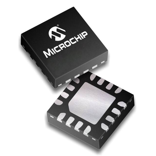
The Supertex MD1810 is a high-speed quad MOSFET driver. It
is designed to drive high voltage P- and N-channel MOSFETs for
medical ultrasound imaging applications. The MD1810 can also be
used for ultrasound metal flaw detection, Non-Destructive Testing
(NDT), piezoelectric transducer drive, clock drive, and PIN diode
drive.
The MD1810 has four inputs which individually control four outputs.
It also has an output enable (OE) pin. When OE is low, all of the
outputs will be in a high impedence state regardless of their logic
input control. When OE is high, the MD1810 sets the threshold logic
transition to (VOE+VGND)/2. This ensures the transition to always be
at half the amplitude of the logic input signal. This allows the device
to have inherent propagation delay matching regardless of the logic
input amplitude.
Applications
►►
►►
►►
►►
►►
►►
Medical ultrasound imaging
Piezoelectric transducer drivers
Non-Destructive Testing (NDT)
PIN diode driver
CCD Clock driver/buffer
High speed level translator
The output stage of the MD1810 has separate power connections
enabling the output signal L and H levels to be chosen independently
from the VDD and VSS supply voltages. As an example, the input logic
levels may be 0 and 1.8V, the control logic may be powered by +5.0
and -5.0V, and the output L and H levels may be varied anywhere
over the range of -5.0 to +5.0V. The output stage is capable of peak
currents of up to ±2.0A, depending on the supply voltages used and
Typical Application Circuit
+100V
+12V
+12V
1.0μF
0.47μF
0.47μF
VDD
VH
10nF
OE
INA
OUTA
10nF
-100V
1.0μF
INB
TC6320
OUTB
3.3V CMOS
Logic Inputs
+10V
OUTC
INC
OUTD
IND
1.0μF
10nF
GND VSS VL
MD1810
10nF
-10V
TC6320
Supertex inc.
1.0μF
● 1235 Bordeaux Drive, Sunnyvale, CA 94089 ● Tel: 408-222-8888 ● www.supertex.com
�MD1810
Ordering Information
16-Lead QFN
4.00x4.00mm body
1.00mm height (max)
0.65mm pitch
Device
MD1810
MD1810K6-G
-G indicates package is RoHS compliant (‘Green’)
Absolute Maximum Ratings
Parameter
Value
VDD -VSS, Logic supply voltage
16
-0.5V to +13.5V
VH, Output high supply voltage
VL - 0.5V to VDD +0.5V
VL, Output low supply voltage
VSS - 0.5V to VH+0.5V
VSS, Low side supply voltage
1
-7.0V to +0.5V
Logic input levels
VSS - 0.5V to GND +7V
Maximum junction temperature
+125°C
Storage temperature
-65°C to 150°C
Operating temperature
-20°C to +85°C
Package power dissipation
2.2W
Thermal resistance (θJA)*
16-Lead QFN (K6)
(top view)
Product Marking
45°C/W
Absolute Maximum Ratings are those values beyond which damage to the device
may occur. Functional operation under these conditions is not implied. Continuous
operation of the device at the absolute rating level may affect device reliability. All
voltages are referenced to device ground.
* 1.0oz 4-layer 3x4” PCB
Y = Last Digit of Year Sealed
W = Code for Week Sealed
L = Lot Number
= “Green” Packaging
1810
YWLL
Package may or may not include the following marks: Si or
16-Lead QFN (K6)
DC Electrical Characteristics (V
H
Sym
Pin Configuration
= VDD = 12V, VL = VSS = GND = 0V, VOE = 3.3V, TA = 25°C)
Parameter
Min
Typ
Max
Units
Logic supply voltage
4.5
-
13
V
2.5V ≤ VDD ≤13V
VSS
Low side supply voltage
-5.5
-
0
V
---
VH
Output high supply voltage
VSS +2
-
VDD
V
---
VL
Output low supply voltage
VSS
-
VDD -2
V
---
VDD - VSS
IDDQ
VDD quiescent current
-
0.8
-
mA
IHQ
VH quiescent current
-
-
10
µA
IDD
VDD average current
-
7.0
-
mA
IH
VH average current
-
18
-
mA
VIH
Input logic voltage high
VOE -0.3
-
5.0
V
VIL
Input logic voltage low
0
-
0.3
V
IIH
Input logic current high
-
1.0
µA
IIL
Input logic current low
-
-
1.0
µA
VIH
OE input logic voltage high
1.7
-
5.0
V
VIL
OE input logic voltage low
0
-
0.3
V
RIN
Input logic impedance to GND
10
20
30
KΩ
CIN
Logic input capacitance
-
5.0
10
pF
Supertex inc.
Conditions
No input transitions, OE = 1
One channel on at 5.0Mhz,
No load
For logic inputs INA, INB, INC, and
IND
For logic input OE
---
● 1235 Bordeaux Drive, Sunnyvale, CA 94089 ● Tel: 408-222-8888 ● www.supertex.com
2
�MD1810
DC Electrical Characteristics (cont.) (V
H
Sym
Parameter
RSINK
= VDD = 12V, VL = VSS = GND = 0V, VOE = 3.3V, TA = 25°C)
Min
Typ
Max
Units
Conditions
Output sink resistance
-
-
12.5
Ω
ISINK = 50mA
RSOURCE
Output source resistance
-
-
12.5
Ω
ISOURCE = 50mA
ISINK
Peak output sink current
-
2.0
-
A
---
Peak output source current
-
2.0
-
A
---
ISOURCE
AC Electrical Characteristics (V
H
Sym
tirf
tPLH
tPHL
Parameter
Input or OE rise & fall time
Propagation delay when output
is from low to high
Propagation delay when output
is from high to low
= VDD = 12V, VL = VSS = GND = 0V, VOE = 3.3V, TA = 25°C)
Min
Typ
Max
Units
-
-
10
ns
-
7.0
-
ns
-
7.0
-
ns
tr
Output rise time
-
6.0
-
ns
tf
Output fall time
-
6.0
-
ns
Rise and fall time matching
-
1.0
-
Propagation low to high and high
to low matching
-
1.0
-
Propagation delay matching
-
±2.0
-
-
200
-
-
9.0
-
l tr - tf l
l tPLH-tPHL l
∆tdm
tOE_ON
tOE_OFF
Output enable time
Conditions
Logic input edge speed requirement
CLOAD = 1000pF, see timing diagram
Input signal rise/fall time 2.0ns
ns
For each channel
ns
Device to device delay match
ns
---
Logic Truth Table
Logic Inputs
Output
OE
IN
H
L
VL
H
H
VH
L
X
High Z
Timing Diagram
VTH / VOE Curve
3.3V
INPUT
50%
50%
tPLH
tPHL
12V
0V
VOE/2
2.0
0V
OUTPUT
VTH vs VOE
90%
1.5
VTH
90%
1.0
10%
10%
tr
tf
0.6V
0.5
0
0
1.0
2.0
3.0
4.0
5.0
VOE
Supertex inc.
● 1235 Bordeaux Drive, Sunnyvale, CA 94089 ● Tel: 408-222-8888 ● www.supertex.com
3
�MD1810
Simplified Block Diagram
VDD
VH
OE
INA
OUTA
INB
OUTB
INC
OUTC
IND
OUTD
MD1810
GND VSS
VL
Detailed Block Diagram
VDD
OE
VH
Level
Shifter
VSS
OUTA
VDD
INA
Level
Shifter
VSS
VDD
VL
VH
VSS
OUTB
VDD
INB
Level
Shifter
VSS
VL
VDD
VH
VSS
OUTC
VDD
INC
Level
Shifter
VSS
VL
VH
VDD
VSS
OUTD
VDD
IND
Level
Shifter
SUB
GND
Supertex inc.
VSS
VL
● 1235 Bordeaux Drive, Sunnyvale, CA 94089 ● Tel: 408-222-8888 ● www.supertex.com
4
�MD1810
Typical Applications
2-Channel +100V to -100V Pulser
+100V
+12V
+12V
0.1μF
0.47μF
0.47μF
VDD
10nF
VH
To Piezoelectric
Transducer
OE
INA
OUTA
OUTB
INB
3.3V CMOS
Logic Inputs
10nF
-100V
OUTC
INC
0.1μF
Supertex
TC6320TG
+100V
0.1μF
OUTD
IND
10nF
To Piezoelectric
Transducer
GND VSS VL
Supertex
MD1810
10nF
-100V
0.1μF
Supertex
TC6320TG
Single Channel ±100V to 0V Pulser
+100V
+5.0V
+5.0V
0.1μF
0.47μF
0.47μF
VDD
10nF
VH
To Piezoelectric
Transducer
OE
INA
OUTA
INB
OUTB
3.3V CMOS
Logic Inputs
INC
Supertex
TC6320
0.1μF
OUTD
GND VSS VL
0.47μF
Supertex inc.
-100V
OUTC
IND
-5.0V
10nF
Supertex
MD1810
-5.0V
0.47μF
Supertex
TC2320
● 1235 Bordeaux Drive, Sunnyvale, CA 94089 ● Tel: 408-222-8888 ● www.supertex.com
5
�MD1810
Application Information
For proper operation of the MD1810, low inductance bypass
capacitors should be used on the various supply pins. The
GND pin should be connected to the logic ground. The INA,
INB INC, IND, and OE pins should be connected to a logic
source with a swing of GND to OE, where OE is 1.8 to 5.0 V.
Good trace practices should be followed corresponding to the
desired operating speed. The internal circuitry of the MD1810
is capable of operating up to 100MHz, with the primary speed
limitation being the loading effects of the load capacitance.
Because of this speed and the high transient currents that
result with capacitive loads, the bypass capacitors should
be as close to the chip pins as possible. Unless the load
specifically requires bipolar drive, the VSS, and VL pins should
have low inductance feed-through connections directly to a
ground plane. If these voltages are not zero, then they need
bypass capacitors in a manner similar to the positive power
supplies. The power connection VDD should have a ceramic
bypass capacitor to the ground plane with short leads and
decoupling components to prevent resonance in the power
leads.
The voltages of VH and VL decide the output signal levels.
These two pins can draw fast transient currents of up to
2.0A, so they should be provided with an appropriate bypass
Supertex inc.
capacitor located next to the chip pins. A ceramic capacitor
of up to 1.0µF may be appropriate, with a series ferrite bead
to prevent resonance in the power supply lead coming to
the capacitor. Pay particular attention to minimizing trace
lengths, current loop area and using sufficient trace width to
reduce inductance. Surface mount components are highly
recommended. Since the output impedance of this driver is
very low, in some cases it may be desirable to add a small
series resistance in series with the output signal to obtain
better waveform transitions at the load terminals. This will of
course reduce the output voltage slew rate at the terminals
of a capacitive load.
Pay particular attention that parasitic couplings are minimized
from the output to the input signal terminals. The parasitic
feedback may cause oscillations or spurious waveform
shapes on the edges of signal transitions. Since the input
operates with signals down to 1.8V even small coupled
voltages may cause problems. Use of a solid ground plane
and good power and signal layout practices will prevent this
problem. Be careful that a circulating ground return current
from a capacitive load cannot react with common inductance
to cause noise voltages in the input logic circuitry.
● 1235 Bordeaux Drive, Sunnyvale, CA 94089 ● Tel: 408-222-8888 ● www.supertex.com
6
�MD1810
Pin Description
Pin #
Function
1
INB
Logic input. Input logic high will cause the output to swing to VH. Input logic low will
cause the output to swing to VL. Keep all logic inputs low until IC powered up.
2
VL
Supply voltage for N-channel output stage.
3
GND
4
VL
Supply voltage for N-channel output stage.
5
INC
6
IND
Logic input. Input logic high will cause the output to swing to VH. Input logic low will
cause the output to swing to VL. Keep all logic inputs low until IC powered up.
7
VSS
8
OUTD
9
OUTC
10, 11
VH
12
OUTB
13
OUTA
14
VDD
High side supply voltage.
15
INA
Logic input. Input logic high will cause the output to swing to VH. Input logic low will
cause the output to swing to VL. Keep all logic inputs low until IC powered up.
16
OE
Output enable logic input. When OE is high, (VOE+VGND)/2 sets the threshold transition
between logic level high and low. When OE is low, all outputs are at high impedance.
Keep OE low until IC powered up.
Substrate
Supertex inc.
Description
Logic input ground reference.
Low side supply voltage. VSS is also connected to the IC substrate. It is required to
connect to the most negative potential of voltage supplies and powered-up first.
Output drivers
Supply voltage for P-channel output stage.
Output drivers
The IC substrate is internally connected to the thermal pad. Thermal pad and VSS
must be connected externally.
● 1235 Bordeaux Drive, Sunnyvale, CA 94089 ● Tel: 408-222-8888 ● www.supertex.com
7
�MD1810
16-Lead QFN Package Outline (K6)
4.00x4.00mm body, 1.00mm height (max), 0.65mm pitch
D
16
D2
Note 1
(Index Area
D/2 x E/2)
16
1
1
e
Note 1
(Index Area
D/2 x E/2)
E
E2
b
Top View
Bottom View
View B
Note 3
θ
L
A
A3
A1
Seating
Plane
L1
Note 2
Side View
View B
Notes:
1. A Pin 1 identifier must be located in the index area indicated. The Pin 1 identifier can be: a molded mark/identifier; an embedded metal marker; or
a printed indicator.
2. Depending on the method of manufacturing, a maximum of 0.15mm pullback (L1) may be present.
3. The inner tip of the lead may be either rounded or square.
Symbol
Dimension
(mm)
A
A1
MIN
0.80
0.00
NOM
0.90
0.02
MAX
1.00
0.05
A3
0.20
REF
b
D
D2
E
E2
e
0.25
3.85*
2.50
3.85*
2.50
0.30
4.00
2.65
4.00
2.65
0.35
4.15*
2.80
4.15*
2.80
0.65
BSC
L
L1
θ
0.00
0O
0.40†
-
-
0.50
0.15
14O
0.30
†
†
JEDEC Registration MO-220, Variation VGGC-2, Issue K, June 2006.
* This dimension is not specified in the JEDEC drawing.
† This dimension differs from the JEDEC drawing.
Drawings not to scale.
Supertex Doc.#: DSPD-16QFNK64X4P065, Version C041009.
(The package drawing(s) in this data sheet may not reflect the most current specifications. For the latest package outline
information go to http://www.supertex.com/packaging.html.)
Supertex inc. does not recommend the use of its products in life support applications, and will not knowingly sell them for use in such applications unless it receives
an adequate “product liability indemnification insurance agreement.” Supertex inc. does not assume responsibility for use of devices described, and limits its liability
to the replacement of the devices determined defective due to workmanship. No responsibility is assumed for possible omissions and inaccuracies. Circuitry and
specifications are subject to change without notice. For the latest product specifications refer to the Supertex inc. (website: http//www.supertex.com)
Supertex inc.
©2012 Supertex inc. All rights reserved. Unauthorized use or reproduction is prohibited.
Doc.# DSFP-MD1810
C011612
8
1235 Bordeaux Drive, Sunnyvale, CA 94089
Tel: 408-222-8888
www.supertex.com
�