MD1811
High-Speed Quad-MOSFET Driver
Features
General Description
•
•
•
•
•
•
•
•
The MD1811 is a high-speed quad-MOSFET driver
designed to drive high-voltage P-channel and
N-channel MOSFETs for medical ultrasound
applications and other applications requiring a
high-output current for a capacitive load. The
high-speed input stage of the MD1811 can operate
from a 1.8V to 5V logic interface with an optimum
operating input signal range of 1.8V to 3.3V. An
adaptive threshold circuit is used to set the level
translator switch threshold to the average of the input
logic 0 and logic 1 levels. The input logic levels may be
ground referenced even though the driver is putting out
bipolar signals. The level translator uses a proprietary
circuit, which provides DC coupling together with
high-speed operation.
6 ns Rise and Fall Time
2A Peak Output Source and Sink Currents
1.8V to 5V Input CMOS Compatible
5V to 12V Total Supply Voltage
Smart Logic Threshold
Low-Jitter Design
Four Matched Channels
Drives Two P-Channel and Two N-Channel
MOSFETs
• Outputs can Swing Below Ground
• Low-Inductance Package
• High-Performance, Thermally Enhanced Package
Applications
•
•
•
•
•
•
The output stage of the MD1811 has separate power
connections, enabling the output signal L and H levels
to be chosen independently from the supply voltages
used for the majority of the circuit. As an example, the
input logic levels may be between 0V and 1.8V, the
control logic may be powered by +5V and –5V, and the
output L and H levels may be varied anywhere over the
range of –5V to +5V. The output stage is capable of
peak currents of up to ±2A, depending on the supply
voltages used and load capacitance present. The OE
pin serves a dual purpose. First, its logic H level is used
to compute the threshold voltage level for the channel
input level translators. Second, when OE is low, the
outputs are disabled, with the A and C outputs high and
the B and D outputs low. This assists in properly
pre-charging the AC coupling capacitors that may be
used in series in the gate drive circuit of an external
PMOS and NMOS transistor pair.
Medical Ultrasound Imaging
Piezoelectric Transducer Drivers
Non-Destructive Testing
PIN Diode Driver
CCD Clock Driver/Buffer
High-Speed Level Translator
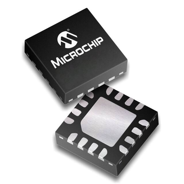
Package Type
16-lead QFN
(Top view)
1
See Table 2-1 for pin information.
2020 Microchip Technology Inc.
DS20005744A-page 1
�MD1811
Functional Block Diagram
Typical Application Circuit
+10V
+10V
0.22µF
ENAB
+PLS1
VDD
OE
-PLS1
+PLS2
10nF
To Piezoelectric
Transducer #1
OUTA
INA
10nF
-100V
OUTB
INB
INC
1.0µF
TC6320
OUTC
#2
-PLS2
1.0µF
VH
#1
3.3V CMOS
Logic Inputs
+100V
0.47µF
+100V
1.0µF
OUTD
IND
GND
VSS
VL
To Piezoelectric
Transducer #2
10nF
MD1811
10nF
-100V
1.0µF
TC6320
DS20005744A-page 2
2020 Microchip Technology Inc.
�MD1811
1.0
ELECTRICAL CHARACTERISTICS
Absolute Maximum Ratings†
Logic Supply Voltage, VDD–VSS ........................................................................................................... –0.5V to +13.5V
Output High Supply Voltage, VH .................................................................................................. VL–0.5V to VDD + 0.5V
Output Low Supply Voltage, VL .................................................................................................... VSS–0.5V to VH+ 0.5V
Low-Side Supply Voltage, VSS .................................................................................................................. –7V to + 0.5V
Logic Input Levels ........................................................................................................................VSS–0.5V to GND +7V
Maximum Junction Temperature, TJ ....................................................................................................................+125°C
Operating Ambient Temperature, TA ..................................................................................................... –20°C to +85°C
Storage Temperature, TS ......................................................................................................................–65°C to +150°C
Power Dissipation ................................................................................................................................................. 2.2W
ESD Rating (Note 1) ............................................................................................................................... ESD Sensitive
† Notice: Stresses above those listed under “Absolute Maximum Ratings” may cause permanent damage to the
device. This is a stress rating only, and functional operation of the device at those or any other conditions above those
indicated in the operational sections of this specification is not intended. Exposure to maximum rating conditions for
extended periods may affect device reliability.
Note 1: Device is ESD sensitive. Handling precautions are recommended.
DC ELECTRICAL CHARACTERISTICS
Electrical Specifications: VH = VDD = 12V, VL = VSS = GND = 0V, VOE = 3.3V, and TA = 25°C
Parameter
Sym.
Min.
Typ.
Max.
Unit
VDD–VSS
4.5
—
13
V
Low-Side Supply Voltage
VSS
–5.5
—
0
V
Output High Supply Voltage
VH
VSS +2
—
VDD
V
Output Low Supply Voltage
VL
VSS
—
VDD –2
V
VDD Quiescent Current
IDDQ
—
0.8
—
mA
VH Quiescent Current
IHQ
—
—
10
µA
VDD Average Current
IDD
—
8
—
mA
VH Average Current
IH
—
26
—
mA
Input Logic Voltage High
VIH
VOE–0.3
—
5
V
Input logic Voltage Low
VIL
0
—
0.3
V
Input Logic Current High
IIH
—
—
1
µA
Input Logic Current Low
IIL
—
—
1
µA
OE Input Logic Voltage High
VIH
1.7
—
5
V
OE Input Logic Voltage Low
VIL
0
—
0.3
V
OE Input Resistance
RIN
10
20
30
kΩ
Logic Input Capacitance
CIN
—
5
10
pF
Logic Supply Voltage
Output Sink Resistance
Output Source Resistance
Peak Output Sink Current
Peak Output Source Current
2020 Microchip Technology Inc.
Conditions
2.5V ≤ VDD ≤ 13V
No input transitions, OE = 1
One channel on at 5 MHz,
no load
For logic inputs INA, INB,
INC, and IND
For logic input OE
RSINK
—
—
12.5
Ω
ISINK = 50 mA
RSOURCE
—
—
12.5
Ω
ISOURCE = 50 mA
ISINK
—
2
—
A
ISOURCE
—
2
—
A
DS20005744A-page 3
�MD1811
AC ELECTRICAL CHARACTERISTICS
Electrical Specifications: VH = VDD = 12V, VL = VSS = GND =0V, VOE = 3.3V and TA = 25°C
Parameter
Sym.
Min.
Typ.
Max.
Unit
Input or OE Rise and Fall
Time
tirf
—
—
10
ns
Propagation Delay when
Output is from Low to High
tPLH
—
7
—
ns
Propagation Delay when
Output is from High to Low
tPHL
—
7
—
ns
Output Rise Time
tr
—
6
—
ns
Output Fall Time
tf
—
6
—
ns
l tr–tf l
—
1
—
ns
l tPLH–tPHL l
—
1
—
ns
Δtdm
—
±2
—
ns
tOE
—
9
—
ns
Min.
Typ.
Max.
Unit
Rise and Fall Time Matching
Propagation Low-to-High
and High-to-Low Matching
Propagation Delay Matching
Output Enable Time
Conditions
Logic input edge speed
requirement
CLOAD = 1000 pF, input signal
rise/fall time of 2 ns (See Timing Diagram)
For each channel
Device-to-device delay match
TEMPERATURE SPECIFICATIONS
Parameter
Sym.
Conditions
TEMPERATURE RANGE
Maximum Junction Temperature
TJ
—
—
125
°C
Operating Ambient Temperature
TA
–20
—
85
°C
Storage Temperature
TS
–65
—
150
°C
JA
—
45
—
°C/W
PACKAGE THERMAL RESISTANCE
16-lead QFN
Note 1:
Note 1
1 oz. 4-layer 3” x 4” PCB
DS20005744A-page 4
2020 Microchip Technology Inc.
�MD1811
Timing Diagram
3.3V
INPUT
50%
50%
0V
tPLH
tPHL
12V
90%
90%
OUTPUT
0V
TABLE 1-1:
10%
10%
tr
tf
TRUTH FUNCTION TABLE
Logic Inputs
Outputs
OE
INA
INB
OUTA
OUTB
H
L
L
VH
VH
H
L
H
VH
VL
H
H
L
VL
VH
H
H
H
VL
VL
L
X
X
OE
INC
IND
VH
OUTC
VL
OUTD
H
L
L
VH
VH
H
L
H
VH
VL
H
H
L
VL
VH
H
H
H
VL
VL
L
X
X
VH
VL
2020 Microchip Technology Inc.
DS20005744A-page 5
�MD1811
2.0
PIN DESCRIPTION
Table 2-1 shows details on the pins of MD1811. See
Package Type for the location of the pins.
TABLE 2-1:
PIN FUNCTION TABLE
Pin Number
Pin Name
1
INB
Logic input. Input logic low will cause the output to swing to VH. Input logic high will
cause the output to swing to VL. Keep all logic inputs low until IC powers up.
2
VL
Supply voltage for N-channel output stage
3
GND
4
VL
Supply voltage for N-channel output stage
5
INC
6
IND
Logic input. Input logic low will cause the output to swing to VH. Input logic high will
cause the output to swing to VL. Keep all logic inputs low until IC powers up.
7
VSS
Low-side supply voltage. VSS is also connected to the IC substrate. It is required to be
connected to the most negative potential of voltage supplies and is powered up first.
8
OUTD
Output driver. Swings from VH to VL. Intended to drive the gate of an external
N-channel MOSFET through a series capacitor. When OE is low, the output is disabled.
OUTD will swing to VL, turning off the external N-channel MOSFET.
9
OUTC
Output driver. Swings from VH to VL. Intended to drive the gate of an external
P-channel MOSFET via a series capacitor. When OE is low, the output is disabled.
OUTC will swing to VH, turning off the external P-channel MOSFET.
10 and 11
VH
12
OUTB
Output driver. Swings from VH to VL. Intended to drive the gate of an external N-channel MOSFET via a series capacitor. When OE is low, the output is disabled. OUTB will
swing to VL, turning off the external N-channel MOSFET.
13
OUTA
Output driver. Swings from VH to VL. Intended to drive the gate of an external P-channel MOSFET through a series capacitor. When OE is low, the output is disabled. OUTA
will swing to VH, turning off the external P-channel MOSFET.
14
VDD
High-side supply voltage
15
INA
Logic input. Input logic low will cause the output to swing to VH. Input logic high will
cause the output to swing to VL. Keep all logic inputs low until the IC powers up.
OE
Output Enable logic input. When OE is high, (VOE+VGND)/2 sets the logic threshold
level for inputs. When OE is low, OUTA and OUTC are at VH, while OUTB and OUTD
are at VL regardless of the inputs INA, INB, INC, or IND. Keep OE low until IC powers
up.
16
Substrate
DS20005744A-page 6
Description
Logic input ground reference
Supply voltage for P-channel output stage
The IC substrate is internally connected to the thermal pad. Thermal Pad and VSS
must be connected externally.
2020 Microchip Technology Inc.
�MD1811
3.0
APPLICATION INFORMATION
For proper operation of the MD1811, low-inductance
bypass capacitors should be used on the various
supply pins. The GND input pin should be connected to
the logic ground. The INA, INB, INC, IND, and OE pins
should be connected to a logic source with a swing of
GND to OE, where OE is 1.8V to 5V. Good trace
practices should be followed corresponding to the
desired operating speed. The internal circuitry of the
MD1811 is capable of operating up to 100 MHz, with
the primary speed limitation being the loading effect of
the load capacitance. Because of this speed and the
high transient currents due to the capacitive loads, the
bypass capacitors should be as close to the chip pins
as possible. Unless the load specifically requires
bipolar drive, the VSS and VL pins should have
low-inductance feed-through connections directly to a
ground plane. The power connection VDD should have
a ceramic bypass capacitor to the ground plane with
short leads and decoupling components to prevent
resonance in the power leads.
The voltages of VH and VL decide the output logic
levels. These two pins can draw fast transient currents
of up to 2A, so they should be provided with a suitable
bypass capacitor located next to the chip pins. A
ceramic capacitor of up to 1 µF may be appropriate,
with a series ferrite bead to prevent resonance in the
power supply lead going to the capacitor.
Pay particular attention to minimizing trace lengths,
current loop area, and using sufficient trace width to
reduce inductance. Surface-mount components are
highly recommended. Since the output impedance of
this driver is very low, in some cases, it may be
desirable to add a small series resistor in series with
the output signal to obtain better waveform transitions
at the load terminals. This will reduce the output
voltage slew rate at the terminals of a capacitive load.
Ensure that parasitic couplings are minimized from the
driver output to the input signal terminals. The parasitic
feedback may cause oscillations or spurious waveform
shapes on the edges of signal transitions. Since the
input operates with signals down to 1.8V, even small
coupled voltages may cause problems. The use of a
solid ground plane as well as good power and signal
layout practices will prevent this problem. Make sure
that the circulating ground return current from a
capacitive load will not react with common inductance
and cause noise voltages in the input logic circuitry.
2020 Microchip Technology Inc.
DS20005744A-page 7
�MD1811
4.0
PACKAGING INFORMATION
4.1
Package Marking Information
16-lead QFN
XX
XXXXXX
e3 YYWW
NNN
Legend: XX...X
Y
YY
WW
NNN
e3
*
Note:
DS20005744A-page 8
Example
MD
1811K6
e3 2025
521
Product Code or Customer-specific information
Year code (last digit of calendar year)
Year code (last 2 digits of calendar year)
Week code (week of January 1 is week ‘01’)
Alphanumeric traceability code
Pb-free JEDEC® designator for Matte Tin (Sn)
This package is Pb-free. The Pb-free JEDEC designator ( e3 )
can be found on the outer packaging for this package.
In the event the full Microchip part number cannot be marked on one line, it will
be carried over to the next line, thus limiting the number of available characters
for product code or customer-specific information. Package may or not include
the corporate logo.
2020 Microchip Technology Inc.
�MD1811
Note: For the most current package drawings, see the Microchip Packaging Specification at www.microchip.com/packaging.
2020 Microchip Technology Inc.
DS20005744A-page 9
�MD1811
NOTES:
DS20005744A-page 10
2020 Microchip Technology Inc.
�MD1811
APPENDIX A:
REVISION HISTORY
Revision A (September 2020)
• Converted Supertex Doc# DSFP-MD1811 to
Microchip DS20005744A
• Changed the package marking format
• Updated the quantity of the 16-lead QFN K6 package from 3000/Reel to 3300/Reel to align it with
the actual BQM
• Made minor text changes throughout the document
2020 Microchip Technology Inc.
DS20005744A-page 11
�MD1811
PRODUCT IDENTIFICATION SYSTEM
To order or obtain information, e.g., on pricing or delivery, contact your local Microchip representative or sales office.
XX
PART NO.
-
Package
Options
Device
X
-
Environmental
X
Media Type
Device:
MD1811
=
High-Speed Quad-MOSFET Driver
Package:
K6
=
16-lead QFN
Environmental:
G
=
Lead (Pb)-free/RoHS-compliant Package
Media Type:
(blank)
=
3300/Reel for a K6 Package
DS20005744A-page 12
Example:
a) MD1811K6-G:
High-Speed Quad-MOSFET
Driver, 16-lead QFN,
3300/Reel
2020 Microchip Technology Inc.
�Note the following details of the code protection feature on Microchip devices:
•
Microchip products meet the specifications contained in their particular Microchip Data Sheet.
•
Microchip believes that its family of products is secure when used in the intended manner and under normal conditions.
•
There are dishonest and possibly illegal methods being used in attempts to breach the code protection features of the Microchip
devices. We believe that these methods require using the Microchip products in a manner outside the operating specifications
contained in Microchip's Data Sheets. Attempts to breach these code protection features, most likely, cannot be accomplished
without violating Microchip's intellectual property rights.
•
Microchip is willing to work with any customer who is concerned about the integrity of its code.
•
Neither Microchip nor any other semiconductor manufacturer can guarantee the security of its code. Code protection does not
mean that we are guaranteeing the product is "unbreakable." Code protection is constantly evolving. We at Microchip are
committed to continuously improving the code protection features of our products. Attempts to break Microchip's code protection
feature may be a violation of the Digital Millennium Copyright Act. If such acts allow unauthorized access to your software or
other copyrighted work, you may have a right to sue for relief under that Act.
Information contained in this publication is provided for the sole
purpose of designing with and using Microchip products. Information regarding device applications and the like is provided
only for your convenience and may be superseded by updates.
It is your responsibility to ensure that your application meets
with your specifications.
THIS INFORMATION IS PROVIDED BY MICROCHIP "AS IS".
MICROCHIP MAKES NO REPRESENTATIONS OR WARRANTIES OF ANY KIND WHETHER EXPRESS OR IMPLIED,
WRITTEN OR ORAL, STATUTORY OR OTHERWISE,
RELATED TO THE INFORMATION INCLUDING BUT NOT
LIMITED
TO ANY
IMPLIED
WARRANTIES
OF
NON-INFRINGEMENT, MERCHANTABILITY, AND FITNESS
FOR A PARTICULAR PURPOSE OR WARRANTIES
RELATED TO ITS CONDITION, QUALITY, OR PERFORMANCE.
IN NO EVENT WILL MICROCHIP BE LIABLE FOR ANY INDIRECT, SPECIAL, PUNITIVE, INCIDENTAL OR CONSEQUENTIAL LOSS, DAMAGE, COST OR EXPENSE OF ANY KIND
WHATSOEVER RELATED TO THE INFORMATION OR ITS
USE, HOWEVER CAUSED, EVEN IF MICROCHIP HAS
BEEN ADVISED OF THE POSSIBILITY OR THE DAMAGES
ARE FORESEEABLE. TO THE FULLEST EXTENT
ALLOWED BY LAW, MICROCHIP'S TOTAL LIABILITY ON
ALL CLAIMS IN ANY WAY RELATED TO THE INFORMATION
OR ITS USE WILL NOT EXCEED THE AMOUNT OF FEES, IF
ANY, THAT YOU HAVE PAID DIRECTLY TO MICROCHIP
FOR THE INFORMATION. Use of Microchip devices in life support and/or safety applications is entirely at the buyer's risk, and
the buyer agrees to defend, indemnify and hold harmless
Microchip from any and all damages, claims, suits, or expenses
resulting from such use. No licenses are conveyed, implicitly or
otherwise, under any Microchip intellectual property rights
unless otherwise stated.
Trademarks
The Microchip name and logo, the Microchip logo, Adaptec,
AnyRate, AVR, AVR logo, AVR Freaks, BesTime, BitCloud, chipKIT,
chipKIT logo, CryptoMemory, CryptoRF, dsPIC, FlashFlex,
flexPWR, HELDO, IGLOO, JukeBlox, KeeLoq, Kleer, LANCheck,
LinkMD, maXStylus, maXTouch, MediaLB, megaAVR, Microsemi,
Microsemi logo, MOST, MOST logo, MPLAB, OptoLyzer,
PackeTime, PIC, picoPower, PICSTART, PIC32 logo, PolarFire,
Prochip Designer, QTouch, SAM-BA, SenGenuity, SpyNIC, SST,
SST Logo, SuperFlash, Symmetricom, SyncServer, Tachyon,
TempTrackr, TimeSource, tinyAVR, UNI/O, Vectron, and XMEGA
are registered trademarks of Microchip Technology Incorporated in
the U.S.A. and other countries.
APT, ClockWorks, The Embedded Control Solutions Company,
EtherSynch, FlashTec, Hyper Speed Control, HyperLight Load,
IntelliMOS, Libero, motorBench, mTouch, Powermite 3, Precision
Edge, ProASIC, ProASIC Plus, ProASIC Plus logo, Quiet-Wire,
SmartFusion, SyncWorld, Temux, TimeCesium, TimeHub,
TimePictra, TimeProvider, Vite, WinPath, and ZL are registered
trademarks of Microchip Technology Incorporated in the U.S.A.
Adjacent Key Suppression, AKS, Analog-for-the-Digital Age, Any
Capacitor, AnyIn, AnyOut, BlueSky, BodyCom, CodeGuard,
CryptoAuthentication, CryptoAutomotive, CryptoCompanion,
CryptoController, dsPICDEM, dsPICDEM.net, Dynamic Average
Matching, DAM, ECAN, EtherGREEN, In-Circuit Serial
Programming, ICSP, INICnet, Inter-Chip Connectivity, JitterBlocker,
KleerNet, KleerNet logo, memBrain, Mindi, MiWi, MPASM, MPF,
MPLAB Certified logo, MPLIB, MPLINK, MultiTRAK, NetDetach,
Omniscient Code Generation, PICDEM, PICDEM.net, PICkit,
PICtail, PowerSmart, PureSilicon, QMatrix, REAL ICE, Ripple
Blocker, SAM-ICE, Serial Quad I/O, SMART-I.S., SQI,
SuperSwitcher, SuperSwitcher II, Total Endurance, TSHARC,
USBCheck, VariSense, ViewSpan, WiperLock, Wireless DNA, and
ZENA are trademarks of Microchip Technology Incorporated in the
U.S.A. and other countries.
SQTP is a service mark of Microchip Technology Incorporated in
the U.S.A.
The Adaptec logo, Frequency on Demand, Silicon Storage
Technology, and Symmcom are registered trademarks of Microchip
Technology Inc. in other countries.
GestIC is a registered trademark of Microchip Technology Germany
II GmbH & Co. KG, a subsidiary of Microchip Technology Inc., in
other countries.
All other trademarks mentioned herein are property of their
respective companies.
© 2020, Microchip Technology Incorporated, All Rights Reserved.
For information regarding Microchip’s Quality Management Systems,
please visit www.microchip.com/quality.
2020 Microchip Technology Inc.
ISBN: 978-1-5224-6856-1
DS20005744A-page 13
�Worldwide Sales and Service
AMERICAS
ASIA/PACIFIC
ASIA/PACIFIC
EUROPE
Corporate Office
2355 West Chandler Blvd.
Chandler, AZ 85224-6199
Tel: 480-792-7200
Fax: 480-792-7277
Technical Support:
http://www.microchip.com/
support
Web Address:
www.microchip.com
Australia - Sydney
Tel: 61-2-9868-6733
India - Bangalore
Tel: 91-80-3090-4444
China - Beijing
Tel: 86-10-8569-7000
India - New Delhi
Tel: 91-11-4160-8631
Austria - Wels
Tel: 43-7242-2244-39
Fax: 43-7242-2244-393
China - Chengdu
Tel: 86-28-8665-5511
India - Pune
Tel: 91-20-4121-0141
China - Chongqing
Tel: 86-23-8980-9588
Japan - Osaka
Tel: 81-6-6152-7160
China - Dongguan
Tel: 86-769-8702-9880
Japan - Tokyo
Tel: 81-3-6880- 3770
China - Guangzhou
Tel: 86-20-8755-8029
Korea - Daegu
Tel: 82-53-744-4301
China - Hangzhou
Tel: 86-571-8792-8115
Korea - Seoul
Tel: 82-2-554-7200
China - Hong Kong SAR
Tel: 852-2943-5100
Malaysia - Kuala Lumpur
Tel: 60-3-7651-7906
China - Nanjing
Tel: 86-25-8473-2460
Malaysia - Penang
Tel: 60-4-227-8870
China - Qingdao
Tel: 86-532-8502-7355
Philippines - Manila
Tel: 63-2-634-9065
China - Shanghai
Tel: 86-21-3326-8000
Singapore
Tel: 65-6334-8870
China - Shenyang
Tel: 86-24-2334-2829
Taiwan - Hsin Chu
Tel: 886-3-577-8366
China - Shenzhen
Tel: 86-755-8864-2200
Taiwan - Kaohsiung
Tel: 886-7-213-7830
China - Suzhou
Tel: 86-186-6233-1526
Taiwan - Taipei
Tel: 886-2-2508-8600
China - Wuhan
Tel: 86-27-5980-5300
Thailand - Bangkok
Tel: 66-2-694-1351
China - Xian
Tel: 86-29-8833-7252
Vietnam - Ho Chi Minh
Tel: 84-28-5448-2100
Atlanta
Duluth, GA
Tel: 678-957-9614
Fax: 678-957-1455
Austin, TX
Tel: 512-257-3370
Boston
Westborough, MA
Tel: 774-760-0087
Fax: 774-760-0088
Chicago
Itasca, IL
Tel: 630-285-0071
Fax: 630-285-0075
Dallas
Addison, TX
Tel: 972-818-7423
Fax: 972-818-2924
Detroit
Novi, MI
Tel: 248-848-4000
Houston, TX
Tel: 281-894-5983
Indianapolis
Noblesville, IN
Tel: 317-773-8323
Fax: 317-773-5453
Tel: 317-536-2380
Los Angeles
Mission Viejo, CA
Tel: 949-462-9523
Fax: 949-462-9608
Tel: 951-273-7800
Raleigh, NC
Tel: 919-844-7510
New York, NY
Tel: 631-435-6000
San Jose, CA
Tel: 408-735-9110
Tel: 408-436-4270
Canada - Toronto
Tel: 905-695-1980
Fax: 905-695-2078
DS20005744A-page 14
China - Xiamen
Tel: 86-592-2388138
China - Zhuhai
Tel: 86-756-3210040
Denmark - Copenhagen
Tel: 45-4485-5910
Fax: 45-4485-2829
Finland - Espoo
Tel: 358-9-4520-820
France - Paris
Tel: 33-1-69-53-63-20
Fax: 33-1-69-30-90-79
Germany - Garching
Tel: 49-8931-9700
Germany - Haan
Tel: 49-2129-3766400
Germany - Heilbronn
Tel: 49-7131-72400
Germany - Karlsruhe
Tel: 49-721-625370
Germany - Munich
Tel: 49-89-627-144-0
Fax: 49-89-627-144-44
Germany - Rosenheim
Tel: 49-8031-354-560
Israel - Ra’anana
Tel: 972-9-744-7705
Italy - Milan
Tel: 39-0331-742611
Fax: 39-0331-466781
Italy - Padova
Tel: 39-049-7625286
Netherlands - Drunen
Tel: 31-416-690399
Fax: 31-416-690340
Norway - Trondheim
Tel: 47-7288-4388
Poland - Warsaw
Tel: 48-22-3325737
Romania - Bucharest
Tel: 40-21-407-87-50
Spain - Madrid
Tel: 34-91-708-08-90
Fax: 34-91-708-08-91
Sweden - Gothenberg
Tel: 46-31-704-60-40
Sweden - Stockholm
Tel: 46-8-5090-4654
UK - Wokingham
Tel: 44-118-921-5800
Fax: 44-118-921-5820
2020 Microchip Technology Inc.
02/28/20
�