MDB1900ZB
Zero Delay Buffer
for PCIe (Gen1/Gen2/Gen3),
SAS, SATA, ESI, and QPI
General Description
Features
The MDB1900ZB is a true zero delay buffer with a fullyintegrated, high-performance, low-power, and low-phase
noise programmable PLL.
• Supports zero delay (0ps) buffer mode for 100MHz and
133MHz clock frequencies.
• External feedback path for true zero delay operations
• Zero delay (PLL) mode can filter jitter in incoming clock
• Selectable PLL bandwidth for PLL mode
• Supports fanout buffer mode for clock frequencies
between 0 and 250MHz
• Differential input reference with HCSL logic (0~0.7V)
• Nineteen differential HCSL-compatible clock output
pairs
• Eight dedicated OE# pins to control their assigned
output. Glitch free assertion/de-assertion.
• Spread spectrum modulation tolerant for EMI reduction
• SMBus interface for controlling output properties
(enable/disable and delay tuning)
• Disabled outputs in power-down mode for maximum
power savings
• Nine selectable SMBus addresses so multiple devices
can share the same SMBus
• 3.3V or 2.5V operation
• Commercial temperature range (0°C to +70°C)
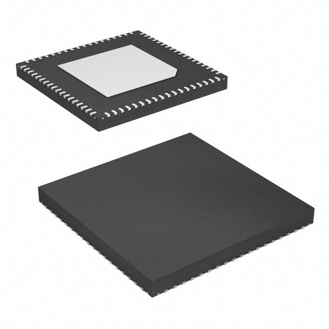
• 72-pin 10mm × 10mm QFN package
• GREEN, RoHS, and PFOS compliant
The MDB1900ZB is capable of distributing the reference
clocks for PCIe (Gen1/Gen2/Gen3), SATA, ESI, SAS, SMI
®
and Intel Quickpath Interconnect (QPI). The MDB1900ZB
works in conjunction with a CK410B+, CK509B or
CK420BQ clock synthesizer to provide reference clocks to
multiple agents.
The MDB1900ZB is designed for Intel’s DB1900Z
specification. The Intel part designation for the
MDB1900ZB is identified as G20746-002.
Datasheets and support documentation are available on
Micrel’s web site at: www.micrel.com.
Block Diagram
Applications
• PCI Express timing (Gen1/2/3) in Intel platforms,
specifically the Romley platform
• SATA / SAS timing (storage)
• ESI and SMI systems (storage)
• Intel Quickpath Interconnect
Key Specifications
•
•
•
•
•
•
Cycle-to-cycle jitter (PLL mode):
很抱歉,暂时无法提供与“MDB1900ZBQZ-TR”相匹配的价格&库存,您可以联系我们找货
免费人工找货