MIC2285A
8MHz PWM Synchronous Buck Regulator
with LDO Standby Mode
General Description
Features
The Micrel MIC2285A is a high efficiency 8MHz
PWM synchronous buck (step-down) regulator that
features a LOWQ® LDO standby mode that draws
only 20µA of quiescent current. The MIC2285A
allows an ultra-low noise, small size, and high
efficiency solution for portable power applications.
In PWM mode, the MIC2285A operates with a
constant frequency 8MHz PWM control. Under light
load conditions, such as in system sleep or standby
modes, the PWM switching operation can be
disabled to reduce switching losses. In this light load
LOWQ® mode, the LDO maintains the output voltage
and draws only 18µA of quiescent current. The LDO
mode of operation saves battery life while not
introducing spurious noise and high ripple as
experienced with pulse skipping or bursting mode
regulators.
The MIC2285A operates from 2.7V to 5.5V input and
features internal power MOSFETs that can supply
up to 600mA output current in PWM mode. It can
operate with a maximum duty cycle of 100% for use
in low-dropout conditions.
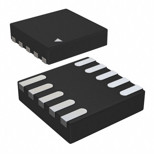
The MIC2285A is available in the 10-pin 2mm x
2mm Thin MLF® package with a junction operating
range from –40°C to +125°C.
Data sheets and support documentation can be
found on Micrel’s web site at: www.micrel.com.
• 2.7 to 5.5V supply/input voltage
• Light load LOWQ® LDO mode
– 20µA quiescent current
– Low noise, 75µVrms
• 8MHz PWM mode
– Output current to 600mA
– >90% efficiency
– 100% maximum duty cycle
• Adjustable output voltage option down to 1V
– Fixed output voltage options available
• Ultra-fast transient response
• Requires only a 0.47µH inductor
• Enables sub 0.55mm profile solution
• Fully integrated MOSFET switches
• Micropower shutdown
• Thermal shutdown and current limit protection
• 10-pin 2mm x 2mm x 0.55mm MLF® package
• –40°C to +125°C junction temperature range
Applications
• Cellular phones
• PDAs
• USB peripherals
____________________________________________________________________________________________________
Typical Application
2.5VOUT Efficiency
100
90
80
70
60
50
V IN =3.2V
VIN =3.6V
VIN =4.2V
40
30
20
Adjustable Output Buck Regulator with LOWQ® Mode
10
0
0
100 200 300 400 500 600
OUTPUT CURRENT (mA)
LOWQ is a registered trademark of Micrel, Inc
MLF and MicroLeadFrame are registered trademarks of Amkor Technology, Inc.
Micrel, Inc • 2180 Fortune Drive • San Jose, Ca 95131 • USA • tel +1 (408) 944-0800 • fax +1 (408) 474-1000 • http://www.micrel.com
August 2007
M9999-083107-B
�Micrel, Inc.
MIC2285A
Ordering Information
Part Number
MIC2285AYMT
Marking
Output
Voltage*
Junction
Temperature Range
Package
Lead Finish
WPA
Adj.
–40° to +125°C
10-Pin 2x2 Thin MLF®
Pb-free
Note
* For other voltage options available, please contact Micrel Marketing for details.
MLF® is a GREEN RoHS compliant package. Lead finish is NiPdAu. Mold compound is Halogen Free.
Pin Configuration
AGND 1
10 PGND
LDO 2
9
SW
BIAS 3
8
VIN
AVIN
4
7
LOWQ
FB 5
6
EN
10-Pin 2mm x 2mm Thin MLF® (MT)
Pin Description
Pin Number
1
2
3
Pin Name
AGND
LDO
BIAS
4
AVIN
5
FB
6
EN
7
_____
LOWQ
8
9
10
VIN
SW
PGND
August 2007
Pin Function
Analog (signal) Ground.
LDO Output (Output): Connect to VOUT for LDO mode operation.
Internal circuit bias supply. Must be decoupled to signal ground with a 0.1µF
capacitor and should not be loaded.
Analog Supply Voltage (Input): Supply voltage for the analog control circuitry
and LDO input power. Requires bypass capacitor to GND.
Feedback. Input to the error amplifier. For the Adjustable option, connect to the
external resistor divider network to set the output voltage. For fixed output
voltage options, connect to VOUT and an internal resistor network sets the output
voltage.
Enable (Input). Logic low will shut down the device, reducing the quiescent
current to less than 5µA.
Enable LDO Mode (Input): Logic low enables the internal LDO and disables the
PWM operation. Logic high enables the PWM mode and disables the LDO
mode.
Supply Voltage (Input): Supply voltage for the internal switches and drivers.
Switch (Output): Internal power MOSFET output switches.
Power Ground.
2
M9999-083107-B
�Micrel, Inc.
MIC2285A
Absolute Maximum Ratings(1)
Operating Ratings(2)
Supply Voltage (VIN) ............................................ +6V
Output Switch Voltage (VSW) ............................... +6V
Output Switch Current (ISW) ................................... 2A
Logic Input Voltage (VEN,VLOWQ) ..............–0.3V to VIN
Storage Temperature (Ts)............... –60°C to +150°C
ESD Rating(3) ....................................................... 3kV
Supply Voltage (VIN)............................+2.7V to +5.5V
Logic Input Voltage (VEN,VLOWQ) ............. –0.3V to VIN
Junction Temperature (TJ) .............. –40°C to +125°C
Junction Thermal Resistance
2x2 MLF-10L (θJA) ................................... 60°C/W
Electrical Characteristics(4)
VIN = VEN = VLOWQ =3.6V; L = 0.47µH; COUT = 10µF; TA = 25°C, unless noted. Bold values indicate –40°C< TJ < +125°C
Parameter
Condition
Min
Supply Voltage Range
Under-Voltage Lockout
Threshold
Typ
2.7
(turn-on)
2.45
UVLO Hysteresis
2.55
Max
Units
5.5
V
2.65
V
100
mV
Quiescent Current, PWM
mode
VFB = 0.9 * VNOM (not switching)
790
900
µA
Quiescent Current, LDO
mode
VLOWQ = 0V;IOUT = 0mA
20
29
µA
Shutdown Current
VEN = 0V
0.01
5
µA
[Adjustable] Feedback
Voltage
±1%
± 2% (over temperature)
0.99
0.98
1
1.01
1.02
V
V
[Fixed Output] Voltages
Nominal VOUT tolerance
–1
–2
+1
+2
%
%
FB pin input current
1
Current Limit in PWM Mode
VFB = 0.9 * VNOM
Output Voltage Line
Regulation
VOUT > 2V; VIN = VOUT+300mV to 5.5V; ILOAD= 100mA
VOUT < 2V; VIN = 2.7V to 5.5V; ILOAD= 100mA
0.13
Output Voltage Load
Regulation, PWM Mode
20mA < ILOAD < 300mA
0.2
0.8
%
Output Voltage Load
Regulation, LDO Mode
100µA < ILOAD < 50mA
VLOWQ = 0V
0.5
1
%
Maximum Duty Cycle
VFB ≤ 0.4V
PWM Switch ONResistance
ISW = 50mA VFB = 0.7VFB_NOM (High Side Switch)
ISW = -50mA VFB = 1.1VFB_NOM (Low Side Switch)
0.75
1
nA
1.85
A
%
%
100
0.4
0.4
Ω
Ω
Oscillator Frequency
7.2
8
8.8
MHz
LOWQ Threshold Voltage
0.5
0.85
1.3
V
0.1
2
µA
0.85
1.3
V
0.1
2
µA
LOWQ Input Current
Enable Threshold
0.5
Enable Input Current
LDO Dropout Voltage
August 2007
IOUT = 50mA Note 5
110
3
mV
M9999-083107-B
�Micrel, Inc.
MIC2285A
Parameter
Condition
Min
Output Voltage Noise
LOWQ = 0V; COUT = 10µF, 10Hz to 100kHz
LDO Current Limit
LOWQ = 0V; VOUT = 0V (LDO Mode)
Typ
Max
Units
75
µVrms
120
mA
Over-Temperature
Shutdown
160
°C
Over-Temperature
Hysteresis
20
°C
60
Notes
1. Exceeding the absolute maximum rating may damage the device.
2. The device is not guaranteed to function outside its operating rating.
3. Devices are ESD sensitive. Handling precautions recommended. Human body model: 1.5kΩ in series with 100pF.
4. Specification for packaged product only.
5. Dropout voltage is defined as the input-to-output differential at which the output voltage drops 2% below its nominal value that is
initially measured at a 1V differential. For outputs below 2.7V, the dropout voltage is the input-to-output voltage differential with a
minimum input voltage of 2.7V.
August 2007
4
M9999-083107-B
�Micrel, Inc.
MIC2285A
Typical Characteristics – PWM Mode
2.5VOUT Efficiency
1.8VOUT Efficiency
100
90
80
70
60
100
V IN=3.2V
90
V IN=3.2V
VIN=3.6V
VIN=4.2V
80
70
60
100
90 V IN=3.2V
80
VIN=3.6V
70
VIN=4.2V
60
VIN=3.6V
VIN=4.2V
50
40
50
40
50
40
30
30
20
10
20
10
30
20
100 200 300 400 500 600
OUTPUT CURRENT (mA)
0
0
1.2VOUT Efficiency
70
60
VIN=3.6V
VIN=4.2V
50
40
30
30
20
10
20
10
0
0
1100
100 200 300 400 500 600
OUTPUT CURRENT (mA)
Quiescent Current
vs. Input Voltage
0
0
9.0
1000
1.018
1.014
VIN=3.6V
0.998
VIN=3.6V
LowQ=VIN
0.994
0.990
0
100 200 300 400 500 600
OUTPUT CURRENT (mA)
Frequency
vs. Input Voltage
8.0
800
1.5
1.006
1.002
900
7.5
600
2.7 3.1 3.5 3.9 4.3 4.7 5.1 5.5
INPUT VOLTAGE (V)
1.010
VIN=4.2V
8.5
700
100 200 300 400 500 600
OUTPUT CURRENT (mA)
Load Regulation
100
90 V IN=3.2V
80
80
50
40
100 200 300 400 500 600
OUTPUT CURRENT (mA)
1.0VOUT Efficiency
100
90 V IN=3.2V
70
60
10
0
0
1200
CURRENT LIMIT (mA)
0
0
ENABLE THRESHOLD (V)
1.5VOUT Efficiency
7.0
2.7 3.1 3.5 3.9 4.3 4.7 5.1 5.5
INPUT VOLTAGE (V)
100 200 300 400 500 600
OUTPUT CURRENT (mA)
Peak Current Limit
vs. Supply Voltage
1000
800
600
400
200
LowQ = VIN
0
2.7
3.4
4.1
4.8
SUPPLY VOLTAGE (V)
5.5
Enable Threshold
vs. Supply Voltage
1.4
1.3
1.2
1.1
1.0
0.9
0.8
0.7
0.6 LowQ = V
IN
0.5
2.7
3.4
4.1
4.8
SUPPLY VOLTAGE (V)
August 2007
5.5
5
M9999-083107-B
�Micrel, Inc.
MIC2285A
Typical Characteristics - LDO Mode
80
60
40
20
50
40
30
20
10
VOUT = 3.3V
IOUT = 25mA
LowQ = 0V
40
DROPOUT VOLTAGE (mV)
DROPOUT VOLTAGE (mV)
60
0
-40 -20 0 20 40 60 80 100 120
TEMPERATURE (°C)
DROPOUT VOLTAGE (mV)
100
Dropout Voltage
vs. Temperature
70
160
120
0
2.7
80
Current Limit
vs. Supply Voltage
LowQ = 0V
3.4
4.1
4.8
SUPPLY VOLTAGE (V)
120
100
80
60
40
20
Dropout Voltage
vs. Temperature
9
30
25
20
15
10
VOUT = 3.3V
IOUT = 10mA
LowQ = 0V
5
0
-40 -20 0 20 40 60 80 100 120
TEMPERATURE (°C)
VOUT = 3.3V
IOUT = 50mA
LowQ = 0V
0
-40 -20 0 20 40 60 80 100 120
TEMPERATURE (°C)
5.5
35
Dropout Voltage
vs. Temperature
140
DROPOUT VOLTAGE (mV)
CURRENT LIMIT (mA)
140
Dropout Voltage
vs. Temperature
8
7
6
5
4
3
2
1
VOUT = 3.3V
IOUT = 1mA
LowQ = 0V
0
-40 -20 0 20 40 60 80 100 120
TEMPERATURE (°C)
Enable Threshold Voltage
vs. Supply Voltage
ENABLE THRESHOLD (V)
1.5
1.4
1.3
1.2
1.1
1.0
0.9
0.8
0.7
0.6
0.5
2.7
August 2007
LowQ = 0V
3.4
4.1
4.8
SUPPLY VOLTAGE (V)
6
5.5
M9999-083107-B
�Micrel, Inc.
MIC2285A
Typical Characteristics – LDO Mode (cont.)
Quiescent Current
vs. Output Current
24
23
22
21
20
19
18
17
16
15
0
VIN = 3.6V
LowQ = 0V
20
40
60
80
100
OUTPUT CURRENT (mA)
August 2007
Output Voltage
vs. Output Current
1.836
OUTPUT VOLTAGE (V)
QUIESCENT CURRENT (µA)
25
1.827
1.818
1.809
1.8
1.791
1.782
1.773
1.764
0
VIN = 3.6V
VOUT =1.8V
LowQ = 0V
20
40
60
80
100
OUTPUT CURRENT (mA)
7
M9999-083107-B
�Micrel, Inc.
MIC2285A
Functional Diagram
MIC2285A Block Diagram
August 2007
8
M9999-083107-B
�Micrel, Inc.
MIC2285A
Functional Characteristics
Load Transient LDO Mode
Output Current
(20mA/div)
Output Current
(100mA/div)
Output Voltage
AC Coupled
(50mV/div)
Output Voltage
AC Coupled
(50mV/div)
Load Transient PWM Mode
10mA
10mA
COUT = 4.7µF
COUT = 4.7µF
Time (20µs/div)
Time (20µs/div)
Enable Transient LDO Mode
Output Voltage
(1V/div)
0V
Enable
(2V/div)
0V
Enable
(2V/div)
Output Voltage
(1V/div)
Enable Transient PWM Mode
0V
0V
COUT = 4.7µF
COUT = 4.7µF
Time (40µs/div)
Time (40µs/div)
August 2007
9
M9999-083107-B
�Micrel, Inc.
MIC2285A
Functional Description
FB
The feedback pin (FB) provides the control path to
control the output. For adjustable versions, a resistor
divider connecting the feedback to the output is used
to adjust the desired output voltage. The output
voltage is calculated as follows:
VIN
VIN provides power to the MOSFETs for the switch
mode regulator section, along with the current
limiting sensing. Due to the high switching speeds, a
1µF capacitor is recommended close to VIN and the
power ground (PGND) pin for bypassing. Please
refer to layout recommendations.
⎛ R1 ⎞
VOUT = VREF × ⎜
+ 1⎟
⎝ R2 ⎠
AVIN
Analog VIN (AVIN) provides power to the LDO
section. AVIN and VIN must be tied together.
Careful layout should be considered to ensure high
frequency switching noise caused by VIN is reduced
before reaching AVIN.
Where VREF is equal to 1.0V.
A feedforward capacitor is recommended for most
designs using the adjustable output voltage option.
To reduce battery current draw, a 100K feedback
resistor is recommended from the output to the FB
pin (R1). Also, a feedforward capacitor should be
connected between the output and feedback (across
R1). The large resistor value and the parasitic
capacitance of the FB pin can cause a high
frequency pole that can reduce the overall system
phase margin. By placing a feedforward capacitor,
these effects can be significantly reduced. Typically,
an 82pF small ceramic capacitor is recommended.
LDO
The LDO pin is the output of the linear regulator and
should be connected to the output. In LOWQ mode
(LOWQ1.5V), the LDO pin is high
impedance.
EN
The enable pin provides a logic level control of the
output. In the off state, supply current of the device
is greatly reduced (typically
很抱歉,暂时无法提供与“MIC2285AYMT-TR”相匹配的价格&库存,您可以联系我们找货
免费人工找货