MIC23153
4 MHz PWM 2A Buck Regulator with
HyperLight Load® and Power Good
Features
General Description
• Input Voltage: 2.7V to 5.5V
• Output Voltage: Fixed or Adjustable (0.62V to
3.6V)
• Up to 2A Output Current
• Up to 93% Peak Efficiency
• 85% Typical Efficiency at 1 mA
• Power Good (PG) Output
• Programmable Soft-Start
• 22 µA Typical Quiescent Current
• 4 MHz PWM Operation in Continuous Mode
• Ultra-Fast Transient Response
• Low Ripple Output Voltage:
- 35 mVPP Ripple in HyperLight Load® Mode
- 5 mV Output Voltage Ripple in Full PWM
Mode
• Fully Integrated MOSFET Switches
• 0.01 µA Shutdown Current
• Thermal Shutdown and Current Limit Protection
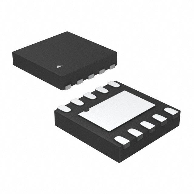
• 10-Pin 2.5 mm x 2.5 mm Thin DFN Package
• –40°C to +125°C Junction Temperature Range
The MIC23153 is a high-efficiency 4 MHz 2A
synchronous buck regulator with HyperLight Load®
mode, Power Good (PG) output indicator, and
programmable soft-start. HyperLight Load® provides
very high efficiency at light loads and ultra-fast
transient response that makes the MIC23153 perfectly
suited for supplying processor core voltages.
Applications
•
•
•
•
•
•
•
Solid State Drives (SSD)
Mobile Handsets
Portable Media/MP3 Players
Portable Navigation Devices (GPS)
WiFi/WiMax/WiBro Modules
Wireless LAN Cards
Portable Applications
2021-2022 Microchip Technology Inc. and its subsidiaries
An additional benefit of this proprietary architecture is
very low output ripple voltage throughout the entire
load range with the use of small output capacitors. The
tiny 2.5 mm x 2.5 mm thin DFN package saves
precious board space and requires only four external
components.
The MIC23153 is designed for use with a very small
inductor, down to 0.47 µH, and an output capacitor as
small as 2.2 µF that enables a total solution size, less
than 1 mm in height.
The MIC23153 has a very-low quiescent current of
22 µA and achieves a peak efficiency of 93% in
continuous conduction mode. In discontinuous
conduction mode, the MIC23153 can achieve 85%
efficiency at 1 mA.
The MIC23153 is available in 10-pin 2.5 mm x 2.5 mm
TDFN package with an operating junction temperature
range from –40°C to +125°C.
DS20006489B-page 1
�MIC23153
Package Types
10-Pin 2.5 mm x 2.5 mm TDFN
Adjustable (Top View)
10-Pin 2.5 mm x 2.5 mm TDFN
Fixed (Top View)
Typical Application Circuits
Fixed Output MIC23153
Adjustable Output MIC23153
DS20006489B-page 2
2021-2022 Microchip Technology Inc. and its subsidiaries
�MIC23153
Functional Block Diagrams
Simplified MIC23153 Fixed Functional Block Diagram
Simplified MIC23153 Adjustable Functional Block Diagram
2021-2022 Microchip Technology Inc. and its subsidiaries
DS20006489B-page 3
�MIC23153
1.0
ELECTRICAL CHARACTERISTICS
Absolute Maximum Ratings †
Supply Voltage (VIN)........................................................................................................................................–0.3 to +6V
Sense Voltage (VSNS) ......................................................................................................................................–0.3 to VIN
Output Switch Voltage (VSW) ...........................................................................................................................–0.3 to VIN
Enable Input Voltage (VEN) ..............................................................................................................................–0.3 to VIN
Power Good (PG) Voltage (VPG)......................................................................................................................–0.3 to VIN
ESD Rating (Note 1)................................................................................................................................... ESD Sensitive
Operating Ratings ‡
Supply Voltage (VIN).................................................................................................................................. +2.7V to +5.5V
Enable Input Voltage (VEN) ................................................................................................................................ 0V to VIN
Sense Voltage (VSNS) ................................................................................................................................. 0.62V to 3.6V
† Notice: Stresses above those listed under “Absolute Maximum Ratings” may cause permanent damage
to the device. This is a stress rating only and functional operation of the device at those or any other conditions above those indicated in the operational sections of this specification is not intended. Exposure to
maximum rating conditions for extended periods may affect device reliability. Specifications are for packaged product only.
‡ Notice: The device is not guaranteed to function outside its operating ratings.
Note 1: Devices are ESD sensitive. Handling precautions are recommended. Human body model, 1.5 kΩ in series
with 100 pF.
ELECTRICAL CHARACTERISTICS
Electrical Characteristics: TA = 25°C, VIN = VEN = 3.6V; L = 1 µH; COUT = 4.7µF; unless otherwise specified. Bold
values indicate –40°C ≤ TJ ≤ +125°C. Specification for packaged product only.
Parameter
Symbol
Min.
Typ.
Max.
Units
Conditions
Supply Voltage Range
—
2.7
—
5.5
V
—
Undervoltage Lockout
Threshold
VUVLO
2.45
2.55
2.65
V
Turn-On
Undervoltage Lockout
Hysteresis
—
—
75
—
mV
—
Quiescent Current
IQ
—
22
45
µA
Shutdown Current
ISHD
—
0.01
5
IOUT = 0 mA, SNS > 1.2 ×
VOUT(NOM)
µA
VEN = 0V; VIN = 5.5V
Output Voltage Accuracy
Feedback Regulation Voltage
Current Limit
Output Voltage Line
Regulation
DS20006489B-page 4
VIN = 3.6V if VOUT(NOM) < 2.5V,
ILOAD = 20 mA
VOUT_ACC
–2.5
—
+2.5
%
VREF
0.6045
0.62
0.635
V
2.2
ILOAD = 20 mA
3.3
—
A
SNS = 0.9 × VOUT(NOM)
ILIM
—
—
—
0.3
%/V
—
VIN = 4.5V if VOUT(NOM) ≥ 2.5V
ILOAD = 20 mA
VIN = 3.6V to 5.5V if
VOUT(NOM) < 2.5V, ILOAD = 20 mA
VIN = 4.5V to 5.5V if
VOUT(NOM) ≥ 2.5V, ILOAD = 20 mA
2021-2022 Microchip Technology Inc. and its subsidiaries
�MIC23153
ELECTRICAL CHARACTERISTICS (CONTINUED)
Electrical Characteristics: TA = 25°C, VIN = VEN = 3.6V; L = 1 µH; COUT = 4.7µF; unless otherwise specified. Bold
values indicate –40°C ≤ TJ ≤ +125°C. Specification for packaged product only.
Parameter
Symbol
Min.
Typ.
Max.
Units
—
0.3
Output Voltage Load
Regulation
—
%
Switching Frequency
20 mA < ILOAD < 500 mA, VIN =
3.6V if VOUT(NOM) < 2.5V
—
20 mA < ILOAD < 500 mA, VIN =
5.0V if VOUT(NOM) ≥ 2.5V
—
20 mA < ILOAD < 1A, VIN = 3.6V if
VOUT(NOM) < 2.5V
—
0.7
—
—
%
—
PWM Switch On-Resistance
Conditions
RDSON,P
—
0.2
RDSON,N
—
0.19
—
FSW
—
4
—
Ω
MHz
20 mA < ILOAD < 1A, VIN = 5.0V if
VOUT(NOM) ≥ 2.5V
ISW = 100 mA PMOS
ISW = –100 mA NMOS
IOUT = 120 mA
Soft-Start Time
—
—
320
—
µs
VOUT = 90%, CSS = 470 pF
Soft-Start Current
—
—
2.7
—
µA
VSS = 0V
Power Good Threshold
(Rising)
—
86
92
96
%
Power Good Threshold
Hysteresis
—
—
7
—
%
Power Good Delay Time
—
—
68
—
µs
Rising
VEN
0.5
0.9
1.2
V
Turn-On
—
—
0.1
2
µA
—
Overtemperature Shutdown
TSHD
—
160
—
°C
—
Overtemperature Shutdown
Hysteresis
TSHD_HYST
—
20
—
°C
Enable Threshold
Enable Input Current
2021-2022 Microchip Technology Inc. and its subsidiaries
—
—
—
DS20006489B-page 5
�MIC23153
TEMPERATURE SPECIFICATIONS (Note 1)
Parameters
Sym.
Min.
Typ.
Max.
Units
Conditions
Junction Temperature Range
TJ
–40
—
+125
°C
Storage Temperature Range
TS
–65
—
+150
°C
—
Lead Temperature
—
—
—
+260
°C
Soldering, 10
seconds
Thermal Resistance TDFN 2.5 mm x 2.5 mm
JA
—
90
—
°C/W
—
Thermal Resistance TDFN 2.5 mm x 2.5 mm
JC
—
63
—
°C/W
—
Temperature Ranges
—
Package Thermal Resistances
Note 1:
The maximum allowable power dissipation is a function of ambient temperature, the maximum allowable
junction temperature and the thermal resistance from junction to air (i.e., TA, TJ, JA). Exceeding the maximum allowable power dissipation will cause the device operating junction temperature to exceed the
maximum +125°C rating. Sustained junction temperatures above +125°C can impact the device reliability.
DS20006489B-page 6
2021-2022 Microchip Technology Inc. and its subsidiaries
�MIC23153
2.0
Note:
TYPICAL PERFORMANCE CURVES
The graphs and tables provided following this note are a statistical summary based on a limited number of
samples and are provided for informational purposes only. The performance characteristics listed herein
are not tested or guaranteed. In some graphs or tables, the data presented may be outside the specified
operating range (e.g., outside specified power supply range) and therefore outside the warranted range.
FIGURE 2-1:
Efficiency vs. Output
Current (VOUT = 1.8V @ 25°C).
FIGURE 2-4:
Voltage.
Current Limit vs Input
FIGURE 2-2:
Efficiency vs. Output
Current (VOUT = 3.3V @ 25°C).
FIGURE 2-5:
Voltage.
Shutdown Current vs Input
FIGURE 2-3:
FIGURE 2-6:
Loads).
Line Regulation (Low
VOUT Rise Time vs. CSS.
2021-2022 Microchip Technology Inc. and its subsidiaries
DS20006489B-page 7
�MIC23153
FIGURE 2-7:
Loads).
Line Regulation (High
FIGURE 2-10:
Temperature.
Output Voltage vs.
FIGURE 2-8:
Current (HLL).
Output Voltage vs. Output
FIGURE 2-11:
Input Voltage.
Power Good Delay Time vs.
FIGURE 2-9:
Current (CCM).
Output Voltage vs. Output
FIGURE 2-12:
Input Voltage.
Power Good Thresholds vs.
DS20006489B-page 8
2021-2022 Microchip Technology Inc. and its subsidiaries
�MIC23153
FIGURE 2-13:
Temperature.
UVLO Threshold vs.
FIGURE 2-16:
Load Current.
Switching Frequency vs.
FIGURE 2-14:
Voltage.
Enable Threshold vs. Input
FIGURE 2-17:
Temperature.
Feedback Voltage vs.
FIGURE 2-15:
Temperature.
Enable Threshold vs.
2021-2022 Microchip Technology Inc. and its subsidiaries
DS20006489B-page 9
�MIC23153
FIGURE 2-18:
Switching Waveform
Discontinuous Mode (Load = 1 mA).
FIGURE 2-21:
Switching Waveform
Continuous Mode (Load = 150 mA).
FIGURE 2-19:
Switching Waveform
Discontinuous Mode (Load = 10 mA).
FIGURE 2-22:
Switching Waveform
Continuous Mode (Load = 500 mA).
FIGURE 2-20:
Switching Waveform
Discontinuous Mode (Load = 50 mA).
FIGURE 2-23:
Switching Waveform
Continuous Mode (Load = 1.5A).
DS20006489B-page 10
2021-2022 Microchip Technology Inc. and its subsidiaries
�MIC23153
FIGURE 2-24:
200 mA).
Load Transient (10 mA to
FIGURE 2-27:
1A).
Load Transient (50 mA to
FIGURE 2-25:
500 mA).
Load Transient (10 mA to
FIGURE 2-28:
1.5A).
Load Transient (50 mA to
FIGURE 2-26:
750 mA).
Load Transient (10 mA to
FIGURE 2-29:
600 mA).
Load Transient (200 mA to
2021-2022 Microchip Technology Inc. and its subsidiaries
DS20006489B-page 11
�MIC23153
FIGURE 2-30:
1A).
Load Transient (200 mA to
FIGURE 2-33:
@ 20 mA Load).
Line Transient (3.6V to 5.5V
FIGURE 2-31:
2A).
Load Transient (200 mA to
FIGURE 2-34:
Waveform.
Start-Up and Power Good
FIGURE 2-32:
@ 1.5A Load).
Line Transient (3.6V to 5.5V
DS20006489B-page 12
2021-2022 Microchip Technology Inc. and its subsidiaries
�MIC23153
3.0
PIN DESCRIPTIONS
The descriptions of the pins are listed in Table 3-1.
TABLE 3-1:
PIN FUNCTION TABLE
Pin Number
(Fixed)
Pin Number
(Adjustable)
Pin
Name
1
1
SW
Switch (Output): Internal power MOSFET output switches.
2
2
EN
Enable (Input): Logic high enables operation of the regulator. Logic
low will shut down the device. Do not leave floating.
3
3
SNS
Sense: Connect to VOUT as close to output capacitor as possible to
sense output voltage.
4
—
NC
Not Internally Connected.
—
4
FB
Feedback: Connect a resistor divider from the output to ground to set
the output voltage.
5
5
PG
Power Good: Open-drain output for the power good indicator. Use a
pull-up resistor from this pin to a voltage source to detect a power
good condition.
6
6
SS
Soft-Start: Place a capacitor from this pin to ground to program the
soft start time. Do not leave floating, 100 pF minimum CSS is
required.
7
7
AGND
8, 9
8, 9
VIN
10
10
PGND
2021-2022 Microchip Technology Inc. and its subsidiaries
Description
Analog Ground: Connect to central ground point where all high
current paths meet (CIN, COUT, PGND) for best operation.
Input Voltage: Connect a capacitor to ground to decouple the noise.
Power Ground.
DS20006489B-page 13
�MIC23153
4.0
FUNCTIONAL DESCRIPTION
4.1
VIN
The input supply (VIN) provides power to the internal
MOSFETs for the switch mode regulator along with the
internal control circuitry. The VIN operating range is
2.7V to 5.5V so an input capacitor, with a minimum
voltage rating of 6.3V, is recommended. Due to the high
switching speed, a minimum 2.2 µF bypass capacitor
placed close to VIN and the power ground (PGND) pin
is required.
4.2
EN
A logic high signal on the enable pin activates the
output voltage of the device. A logic low signal on the
enable pin deactivates the output and reduces supply
current to 0.01 µA. MIC23153 features external soft
start circuitry via the soft-start (SS) pin that reduces in
rush current and prevents the output voltage from
overshooting at start up. Do not leave the EN pin
floating.
4.3
SW
The switch (SW) connects directly to one end of the
inductor and provides the current path during switching
cycles. The other end of the inductor is connected to
the load, SNS pin and output capacitor. Due to the high
speed switching on this pin, the switch node should be
routed away from sensitive nodes whenever possible.
4.4
SNS
The sense (SNS) pin is connected to the output of the
device to provide feedback to the control circuitry. The
SNS connection should be placed close to the output
capacitor.
4.5
4.7
Power Good (PG)
The Power Good (PG) pin is an open drain output
which indicates logic high when the output voltage is
typically above 92% of its steady state voltage. A pull
up resistor of more than 5 kΩ should be connected
from PG to VOUT.
4.8
Soft-Start
The soft-start (SS) pin is used to control the output
voltage ramp up time. The approximate equation for
the ramp time in milliseconds is:
EQUATION 4-1:
3
t ms = 270 10 In 10 C SS
Where:
t=
The time in milliseconds
CSS =
External soft-start capacitance (in Farads)
For example, for a CSS = 470 pF, tRISE ~ 0.3 ms or
300 µs. See Section 2.0, Typical Performance Curves
for a graphical guide. The minimum recommended
value for CSS is 100 pF.
4.9
FB
The feedback (FB) pin is provided for the adjustable
voltage option (no internal connection for fixed
options). This is the control input for programming the
output voltage. A resistor divider network is connected
to this pin from the output and is compared to the
internal 0.62V reference within the regulation loop.
The output voltage can be programmed between 0.65V
and 3.6V using the following equation:
EQUATION 4-2:
R1
V OUT = V REF 1 + -------
R2
AGND
The analog ground (AGND) is the ground path for the
biasing and control circuitry. The current loop for the
signal ground should be separate from the power
ground (PGND) loop.
Where:
4.6
Example feedback resistor values:
PGND
The power ground pin is the ground path for the high
current in PWM mode. The current loop for the power
ground should be as small as possible and separate
from the analog ground (AGND) loop as applicable.
DS20006489B-page 14
R1 =
Top resistor
R2 =
Bottom resistor
TABLE 4-1:
FEEDBACK RESISTOR
VALUES
VOUT
R1
R2
1.2V
274 kΩ
294 kΩ
1.5V
316 kΩ
221 kΩ
1.8V
301 kΩ
158 kΩ
2.5V
324 kΩ
107 kΩ
3.3V
309 kΩ
71.5 kΩ
2021-2022 Microchip Technology Inc. and its subsidiaries
�MIC23153
5.0
APPLICATIONS INFORMATION
The MIC23153 is a high performance DC-to-DC
step-down regulator offering a small solution size.
Supporting an output current up to 2A inside a tiny
2.5 mm x 2.5 mm TDFN package, the IC requires only
three external components while meeting today’s
miniature portable electronic device needs. Using the
HyperLight Load® switching scheme, the MIC23153 is
able to maintain high efficiency throughout the entire
load range while providing ultra-fast load transient
response. The following sections provide additional
device application information.
5.1
Input Capacitor
A 2.2 µF ceramic capacitor or greater should be placed
close to the VIN pin and PGND pin for bypassing. A
Murata GRM188R60J475ME84D, size 0603, 4.7 µF
ceramic capacitor is recommended based upon
performance, size, and cost. A X5R or X7R
temperature rating is recommended for the input
capacitor. Y5V temperature rating capacitors, aside
from losing most of their capacitance over temperature,
can also become resistive at high frequencies. This
reduces their ability to filter out high frequency noise.
5.2
Output Capacitor
The MIC23153 is designed for use with a 2.2 µF or
greater ceramic output capacitor. Increasing the output
capacitance will lower output ripple and improve load
transient response but could also increase solution size
or cost. A low equivalent series resistance (ESR)
ceramic output capacitor such as the Samsung
CL10B475KQ8NQNC, size 0603, 4.7 µF ceramic
capacitor is recommended based upon performance,
size, and cost. Both the X7R or X5R temperature rating
capacitors are recommended. The Y5V and Z5U
temperature rating capacitors are not recommended
due to their wide variation in capacitance over
temperature and increased resistance at high
frequencies.
5.3
EQUATION 5-1:
1 – V OUT V IN
I PEAK = I OUT + V OUT -----------------------------------
2fL
As shown by the calculation above, the peak inductor
current is inversely proportional to the switching
frequency and the inductance; the lower the switching
frequency or the inductance the higher the peak
current. As input voltage increases, the peak current
also increases.
DC resistance (DCR) is also important. While DCR is
inversely proportional to size, DCR can represent a
significant efficiency loss. Refer to the Section 5.6
“Efficiency Considerations”.
The transition between high loads (CCM) to HyperLight
Load® (HLL) mode is determined by the inductor ripple
current and the load current.
Inductor Selection
When selecting an inductor, it is important to consider
the following factors (not necessarily in the order of
importance):
•
•
•
•
Maximum current ratings of the inductor are generally
given in two methods; permissible DC current and
saturation current. Permissible DC current can be rated
either for a 40°C temperature rise or a 10% to 20% loss
in inductance. Ensure the inductor selected can handle
the maximum operating current. When saturation
current is specified, make sure that there is enough
margin so that the peak current does not cause the
inductor to saturate. Peak current can be calculated as
follows:
Inductance
Rated current value
Size requirements
DC resistance (DCR)
The MIC23153 is designed for use with a 0.47 µH to
2.2 µH inductor. For faster transient response, a
0.47 µH inductor will yield the best result. For lower
output ripple, a 2.2 µH inductor is recommended.
2021-2022 Microchip Technology Inc. and its subsidiaries
FIGURE 5-1:
Control Signals.
The diagram shows the signals for high side switch
drive (HSD) for tON control, the inductor current and the
low side switch drive (LSD) for tOFF control.
In HLL mode, the inductor is charged with a fixed Ton
pulse on the high side switch (HSD). After this, the LSD
is switched on and current falls at a rate VOUT/L. The
controller remains in HLL mode while the inductor
falling current is detected to cross approximately
–50 mA. When the LSD (or tOFF) time reaches its
DS20006489B-page 15
�MIC23153
minimum and the inductor falling current is no longer
able to reach this –50 mA threshold, the part is in CCM
mode and switching at a virtually constant frequency.
another DC loss. The current required driving the gates
on and off at a constant 4 MHz frequency and the
switching transitions make up the switching losses.
Once in CCM mode, the tOFF time will not vary.
Therefore, it is important to note that if L is large
enough, the HLL transition level will not be triggered.
That inductor is:
EQUATION 5-2:
V OUT 135ns
L MAX = ---------------------------------2 50mA
5.4
Compensation
The MIC23153 is designed to be stable with a 0.47 µH
to 2.2 µH inductor with a 4.7 µF ceramic (X5R) output
capacitor.
5.5
Duty Cycle
The typical maximum duty cycle of the MIC23153 is
80%.
5.6
Efficiency Considerations
Efficiency is defined as the amount of useful output
power, divided by the amount of power supplied.
EQUATION 5-3:
V OUT I OUT
= -------------------------------- 100
V IN I IN
FIGURE 5-2:
Efficiency Under Load
VOUT = 1.8V @ 25ºC.
Figure 5-2 shows an efficiency curve. From no load to
100 mA, efficiency losses are dominated by quiescent
current losses, gate drive and transition losses. By
using the HyperLight Load® mode, the MIC23153 is
able to maintain high efficiency at low output currents.
Over 100 mA, efficiency loss is dominated by MOSFET
RDS(ON) and inductor losses. Higher input supply
voltages will increase the gate to source threshold on
the internal MOSFETs, thereby reducing the internal
RDS(ON). This improves efficiency by reducing DC
losses in the device. All but the inductor losses are
inherent to the device. In which case, inductor selection
becomes increasingly critical in efficiency calculations.
As the inductors are reduced in size, the DC resistance
(DCR) can become quite significant.
The DCR losses can be calculated by using
Equation 5-4:
EQUATION 5-4:
Maintaining high efficiency serves two purposes. It
reduces power dissipation in the power supply,
reducing the need for heat sinks and thermal design
considerations and it reduces consumption of current
for battery powered applications. Reduced current
draw from a battery increases the devices operating
time which is critical in hand held devices.
There are two types of losses in switching converters;
DC losses and switching losses. DC losses are simply
the power dissipation of I2R. Power is dissipated in the
high-side switch during the on cycle. Power loss is
equal to the high-side MOSFET RDS(ON) multiplied by
the switch current squared. During the off cycle, the
low-side N-channel MOSFET conducts, also
dissipating power. Device operating current also
reduces efficiency. The product of the quiescent
(operating) current and the supply voltage represents
DS20006489B-page 16
2
P DCR = I OUT DCR
From that, the loss in efficiency due to inductor
resistance can be calculated by using Equation 5-5:
EQUATION 5-5:
V OUT I OUT
EfficiencyLoss = 1 – ---------------------------------------------------- 100
V OUT I OUT + P DCR
2021-2022 Microchip Technology Inc. and its subsidiaries
�MIC23153
Efficiency loss due to DCR is minimal at light loads and
gains significance as the load is increased. Inductor
selection becomes a trade-off between efficiency and
size in this case.
5.7
HyperLight Load® Mode
The MIC23153 uses a minimum on and off time
proprietary control loop. When the output voltage falls
below the regulation threshold, the error comparator
begins a switching cycle that turns the PMOS on and
keeps it on for the duration of the minimum on-time.
When the output voltage is over the regulation
threshold, the error comparator turns the PMOS off for
a minimum off-time. The NMOS acts as an ideal
rectifier that conducts when the PMOS is off. Using a
NMOS switch instead of a diode allows for lower
voltage drop across the switching device when it is on.
The asynchronous switching combination between the
PMOS and the NMOS allows the control loop to work
in discontinuous mode for light load operations. In
discontinuous mode, MIC23153 works in pulse
frequency modulation (PFM) to regulate the output. As
the output current increases, the switching frequency
increases. This improves the efficiency of the
MIC23153 during light load currents. As the load
current increases, the MIC23153 goes into continuous
conduction mode (CCM) at a constant frequency of
4 MHz. The equation to calculate the load when the
MIC23153 goes into continuous conduction mode may
be approximated by the following Equation 5-6:
EQUATION 5-6:
V IN – V OUT D
I LOAD = --------------------------------------------
2Lf
As shown in the above equation, the load at which
MIC23153 transitions from HyperLight Load® mode to
PWM mode is a function of the input voltage (VIN),
output voltage (VOUT), duty cycle (D), inductance (L)
and frequency (f). As shown in Figure 5-3, as the
output current increases, the switching frequency also
increases until the MIC23153 goes from HyperLight
Load® mode to PWM mode at approximately 120 mA.
The MIC23153 will switch at a relatively constant
frequency around 4 MHz once the output current is
over 120 mA.
FIGURE 5-3:
Output Current.
2021-2022 Microchip Technology Inc. and its subsidiaries
Switching Frequency vs.
DS20006489B-page 17
�MIC23153
6.0
PACKAGING INFORMATION
6.1
Package Marking Information
Example
10-Lead TDFN*
XXX
NNN
WEG
615
Part Number
Code
MIC23153-GYMT-TR
WEG
MIC23153YMT-TR
WEA
Note:
Legend: XX...X
Y
YY
WW
NNN
e3
*
The content of this table applies
to 10-Lead TDFN.
Product code or customer-specific information
Year code (last digit of calendar year)
Year code (last 2 digits of calendar year)
Week code (week of January 1 is week ‘01’)
Alphanumeric traceability code
Pb-free JEDEC® designator for Matte Tin (Sn)
This package is Pb-free. The Pb-free JEDEC designator ( e3 )
can be found on the outer packaging for this package.
●, ▲, ▼ Pin one index is identified by a dot, delta up, or delta down (triangle
mark).
Note:
In the event the full Microchip part number cannot be marked on one line, it will
be carried over to the next line, thus limiting the number of available
characters for customer-specific information. Package may or may not include
the corporate logo.
Underbar (_) and/or Overbar (‾) symbol may not be to scale.
Note:
If the full seven-character YYWWNNN code cannot fit on the package, the following truncated codes
are used based on the available marking space:
6 Characters = YWWNNN; 5 Characters = WWNNN; 4 Characters = WNNN; 3 Characters = NNN;
2 Characters = NN; 1 Character = N
DS20006489B-page 18
2021-2022 Microchip Technology Inc. and its subsidiaries
�MIC23153
10-Lead TDFN 2.5 mm x 2.5 mm Package Outline and Recommended Land Pattern
Note:
For the most current package drawings, please see the Microchip Packaging Specification located at
http://www.microchip.com/packaging.
2021-2022 Microchip Technology Inc. and its subsidiaries
DS20006489B-page 19
�MIC23153
NOTES:
DS20006489B-page 20
2021-2022 Microchip Technology Inc. and its subsidiaries
�MIC23153
APPENDIX A:
REVISION HISTORY
Revision A (February 2021)
• Converted Micrel document MIC23153 to Microchip data sheet DS20006489B.
• Minor text changes throughout.
Revision B (April 2022)
• Updated Section “Product Identification System”.
• Updated Section 6.0 “Packaging Information”.
• Corrected package outline image to “10-Lead
TDFN 2.5 mm x 2.5 mm Package Outline and
Recommended Land Pattern” from a 10-Lead
TDFN image.
• Minor format changes throughout.
2021-2022 Microchip Technology Inc. and its subsidiaries
DS20006489B-page 21
�MIC23153
NOTES:
DS20006489B-page 22
2021-2022 Microchip Technology Inc. and its subsidiaries
�MIC23153
PRODUCT IDENTIFICATION SYSTEM
To order or obtain information, e.g., on pricing or delivery, contact your local Microchip representative or sales office.
Device
X
-X
PART NO.
Output
Junction
Voltage Temperature
Range
Device:
XX
-XX
Package
Option
Media Type
MIC23153: 4 MHz 2A PWM Buck Regulator with
HyperLight Load® and Power Good
Output Voltage:
G
Blank
= 1.8V
= Adjustable
Junction
Temperature Range:
Y
= –40°C to +125°C
Package:
MT
= 10-Lead 2.5 mm x 2.5 mm x 0.6 mm
TDFN
Media Type:
TR
= 5000/Reel
Examples:
a) MIC23153-GYMT-TR:
4 MHz 2A PWM Buck Regulator
with HyperLight Load® and Power
Good, 1.8V Fixed Output Voltage,
–40°C to +125°C Junction
Temperature Range, Pb-Free,
RoHS Compliant, 10-Lead TDFN
Package, 5000/Reel
b) MIC23153YMT-TR:
4 MHz 2A PWM Buck Regulator
with HyperLight Load® and Power
Good, Adjustable Output Voltage,
–40°C to +125°C Junction
Temperature Range, Pb-Free,
RoHS Compliant, 10-Lead TDFN
Package, 5000/Reel
Note 1:
Tape and Reel identifier only appears in the
catalog part number description. This identifier is
used for ordering purposes and is not printed on
the device package. Check with your Microchip
Sales Office for package availability with the
Tape and Reel option.
Note: Other output voltage options are available. Contact Factory for
details.
2021 - 2022 Microchip Technology Inc. and its subsidiaries
DS20006489B-page 23
�MIC23153
NOTES:
DS20006489B-page 24
2021 - 2022 Microchip Technology Inc. and its subsidiaries
�Note the following details of the code protection feature on Microchip products:
•
Microchip products meet the specifications contained in their particular Microchip Data Sheet.
•
Microchip believes that its family of products is secure when used in the intended manner, within operating specifications, and
under normal conditions.
•
Microchip values and aggressively protects its intellectual property rights. Attempts to breach the code protection features of
Microchip product is strictly prohibited and may violate the Digital Millennium Copyright Act.
•
Neither Microchip nor any other semiconductor manufacturer can guarantee the security of its code. Code protection does not
mean that we are guaranteeing the product is “unbreakable”. Code protection is constantly evolving. Microchip is committed to
continuously improving the code protection features of our products.
This publication and the information herein may be used only
with Microchip products, including to design, test, and integrate
Microchip products with your application. Use of this information in any other manner violates these terms. Information
regarding device applications is provided only for your convenience and may be superseded by updates. It is your responsibility to ensure that your application meets with your
specifications. Contact your local Microchip sales office for
additional support or, obtain additional support at https://
www.microchip.com/en-us/support/design-help/client-supportservices.
THIS INFORMATION IS PROVIDED BY MICROCHIP "AS IS".
MICROCHIP MAKES NO REPRESENTATIONS OR WARRANTIES OF ANY KIND WHETHER EXPRESS OR IMPLIED,
WRITTEN OR ORAL, STATUTORY OR OTHERWISE,
RELATED TO THE INFORMATION INCLUDING BUT NOT
LIMITED TO ANY IMPLIED WARRANTIES OF NONINFRINGEMENT, MERCHANTABILITY, AND FITNESS FOR A
PARTICULAR PURPOSE, OR WARRANTIES RELATED TO
ITS CONDITION, QUALITY, OR PERFORMANCE.
IN NO EVENT WILL MICROCHIP BE LIABLE FOR ANY INDIRECT, SPECIAL, PUNITIVE, INCIDENTAL, OR CONSEQUENTIAL LOSS, DAMAGE, COST, OR EXPENSE OF ANY
KIND WHATSOEVER RELATED TO THE INFORMATION OR
ITS USE, HOWEVER CAUSED, EVEN IF MICROCHIP HAS
BEEN ADVISED OF THE POSSIBILITY OR THE DAMAGES
ARE FORESEEABLE. TO THE FULLEST EXTENT
ALLOWED BY LAW, MICROCHIP'S TOTAL LIABILITY ON
ALL CLAIMS IN ANY WAY RELATED TO THE INFORMATION
OR ITS USE WILL NOT EXCEED THE AMOUNT OF FEES, IF
ANY, THAT YOU HAVE PAID DIRECTLY TO MICROCHIP
FOR THE INFORMATION.
Use of Microchip devices in life support and/or safety applications is entirely at the buyer's risk, and the buyer agrees to
defend, indemnify and hold harmless Microchip from any and
all damages, claims, suits, or expenses resulting from such
use. No licenses are conveyed, implicitly or otherwise, under
any Microchip intellectual property rights unless otherwise
stated.
Trademarks
The Microchip name and logo, the Microchip logo, Adaptec,
AnyRate, AVR, AVR logo, AVR Freaks, BesTime, BitCloud,
CryptoMemory, CryptoRF, dsPIC, flexPWR, HELDO, IGLOO,
JukeBlox, KeeLoq, Kleer, LANCheck, LinkMD, maXStylus,
maXTouch, MediaLB, megaAVR, Microsemi, Microsemi logo,
MOST, MOST logo, MPLAB, OptoLyzer, PIC, picoPower,
PICSTART, PIC32 logo, PolarFire, Prochip Designer, QTouch,
SAM-BA, SenGenuity, SpyNIC, SST, SST Logo, SuperFlash,
Symmetricom, SyncServer, Tachyon, TimeSource, tinyAVR, UNI/O,
Vectron, and XMEGA are registered trademarks of Microchip
Technology Incorporated in the U.S.A. and other countries.
AgileSwitch, APT, ClockWorks, The Embedded Control Solutions
Company, EtherSynch, Flashtec, Hyper Speed Control, HyperLight
Load, IntelliMOS, Libero, motorBench, mTouch, Powermite 3,
Precision Edge, ProASIC, ProASIC Plus, ProASIC Plus logo, QuietWire, SmartFusion, SyncWorld, Temux, TimeCesium, TimeHub,
TimePictra, TimeProvider, TrueTime, WinPath, and ZL are
registered trademarks of Microchip Technology Incorporated in the
U.S.A.
Adjacent Key Suppression, AKS, Analog-for-the-Digital Age, Any
Capacitor, AnyIn, AnyOut, Augmented Switching, BlueSky,
BodyCom, CodeGuard, CryptoAuthentication, CryptoAutomotive,
CryptoCompanion, CryptoController, dsPICDEM, dsPICDEM.net,
Dynamic Average Matching, DAM, ECAN, Espresso T1S,
EtherGREEN, GridTime, IdealBridge, In-Circuit Serial
Programming, ICSP, INICnet, Intelligent Paralleling, Inter-Chip
Connectivity, JitterBlocker, Knob-on-Display, maxCrypto, maxView,
memBrain, Mindi, MiWi, MPASM, MPF, MPLAB Certified logo,
MPLIB, MPLINK, MultiTRAK, NetDetach, NVM Express, NVMe,
Omniscient Code Generation, PICDEM, PICDEM.net, PICkit,
PICtail, PowerSmart, PureSilicon, QMatrix, REAL ICE, Ripple
Blocker, RTAX, RTG4, SAM-ICE, Serial Quad I/O, simpleMAP,
SimpliPHY, SmartBuffer, SmartHLS, SMART-I.S., storClad, SQI,
SuperSwitcher, SuperSwitcher II, Switchtec, SynchroPHY, Total
Endurance, TSHARC, USBCheck, VariSense, VectorBlox, VeriPHY,
ViewSpan, WiperLock, XpressConnect, and ZENA are trademarks
of Microchip Technology Incorporated in the U.S.A. and other
countries.
SQTP is a service mark of Microchip Technology Incorporated in
the U.S.A.
The Adaptec logo, Frequency on Demand, Silicon Storage
Technology, Symmcom, and Trusted Time are registered
trademarks of Microchip Technology Inc. in other countries.
GestIC is a registered trademark of Microchip Technology Germany
II GmbH & Co. KG, a subsidiary of Microchip Technology Inc., in
other countries.
All other trademarks mentioned herein are property of their
respective companies.
© 2021 - 2022, Microchip Technology Incorporated and its subsidiaries.
All Rights Reserved.
For information regarding Microchip’s Quality Management Systems,
please visit www.microchip.com/quality.
2021 - 2022 Microchip Technology Inc. and its subsidiaries
ISBN: 978-1-6683-0342-9
DS20006489B-page 25
�Worldwide Sales and Service
4AMERICAS
ASIA/PACIFIC
ASIA/PACIFIC
EUROPE
Corporate Office
2355 West Chandler Blvd.
Chandler, AZ 85224-6199
Tel: 480-792-7200
Fax: 480-792-7277
Technical Support:
http://www.microchip.com/
support
Web Address:
www.microchip.com
Australia - Sydney
Tel: 61-2-9868-6733
India - Bangalore
Tel: 91-80-3090-4444
China - Beijing
Tel: 86-10-8569-7000
India - New Delhi
Tel: 91-11-4160-8631
Austria - Wels
Tel: 43-7242-2244-39
Fax: 43-7242-2244-393
China - Chengdu
Tel: 86-28-8665-5511
India - Pune
Tel: 91-20-4121-0141
China - Chongqing
Tel: 86-23-8980-9588
Japan - Osaka
Tel: 81-6-6152-7160
China - Dongguan
Tel: 86-769-8702-9880
Japan - Tokyo
Tel: 81-3-6880- 3770
China - Guangzhou
Tel: 86-20-8755-8029
Korea - Daegu
Tel: 82-53-744-4301
China - Hangzhou
Tel: 86-571-8792-8115
Korea - Seoul
Tel: 82-2-554-7200
China - Hong Kong SAR
Tel: 852-2943-5100
Malaysia - Kuala Lumpur
Tel: 60-3-7651-7906
China - Nanjing
Tel: 86-25-8473-2460
Malaysia - Penang
Tel: 60-4-227-8870
China - Qingdao
Tel: 86-532-8502-7355
Philippines - Manila
Tel: 63-2-634-9065
China - Shanghai
Tel: 86-21-3326-8000
Singapore
Tel: 65-6334-8870
China - Shenyang
Tel: 86-24-2334-2829
Taiwan - Hsin Chu
Tel: 886-3-577-8366
China - Shenzhen
Tel: 86-755-8864-2200
Taiwan - Kaohsiung
Tel: 886-7-213-7830
China - Suzhou
Tel: 86-186-6233-1526
Taiwan - Taipei
Tel: 886-2-2508-8600
China - Wuhan
Tel: 86-27-5980-5300
Thailand - Bangkok
Tel: 66-2-694-1351
China - Xian
Tel: 86-29-8833-7252
Vietnam - Ho Chi Minh
Tel: 84-28-5448-2100
Atlanta
Duluth, GA
Tel: 678-957-9614
Fax: 678-957-1455
Austin, TX
Tel: 512-257-3370
Boston
Westborough, MA
Tel: 774-760-0087
Fax: 774-760-0088
Chicago
Itasca, IL
Tel: 630-285-0071
Fax: 630-285-0075
Dallas
Addison, TX
Tel: 972-818-7423
Fax: 972-818-2924
Detroit
Novi, MI
Tel: 248-848-4000
Houston, TX
Tel: 281-894-5983
Indianapolis
Noblesville, IN
Tel: 317-773-8323
Fax: 317-773-5453
Tel: 317-536-2380
Los Angeles
Mission Viejo, CA
Tel: 949-462-9523
Fax: 949-462-9608
Tel: 951-273-7800
Raleigh, NC
Tel: 919-844-7510
New York, NY
Tel: 631-435-6000
San Jose, CA
Tel: 408-735-9110
Tel: 408-436-4270
Canada - Toronto
Tel: 905-695-1980
Fax: 905-695-2078
DS20006489B-page 26
China - Xiamen
Tel: 86-592-2388138
China - Zhuhai
Tel: 86-756-3210040
Denmark - Copenhagen
Tel: 45-4485-5910
Fax: 45-4485-2829
Finland - Espoo
Tel: 358-9-4520-820
France - Paris
Tel: 33-1-69-53-63-20
Fax: 33-1-69-30-90-79
Germany - Garching
Tel: 49-8931-9700
Germany - Haan
Tel: 49-2129-3766400
Germany - Heilbronn
Tel: 49-7131-72400
Germany - Karlsruhe
Tel: 49-721-625370
Germany - Munich
Tel: 49-89-627-144-0
Fax: 49-89-627-144-44
Germany - Rosenheim
Tel: 49-8031-354-560
Israel - Ra’anana
Tel: 972-9-744-7705
Italy - Milan
Tel: 39-0331-742611
Fax: 39-0331-466781
Italy - Padova
Tel: 39-049-7625286
Netherlands - Drunen
Tel: 31-416-690399
Fax: 31-416-690340
Norway - Trondheim
Tel: 47-7288-4388
Poland - Warsaw
Tel: 48-22-3325737
Romania - Bucharest
Tel: 40-21-407-87-50
Spain - Madrid
Tel: 34-91-708-08-90
Fax: 34-91-708-08-91
Sweden - Gothenberg
Tel: 46-31-704-60-40
Sweden - Stockholm
Tel: 46-8-5090-4654
UK - Wokingham
Tel: 44-118-921-5800
Fax: 44-118-921-5820
2021 - 2022 Microchip Technology Inc. and its subsidiaries
09/14/21
�


 工商网监
湘ICP备2023018690号
工商网监
湘ICP备2023018690号
