MIC261201
28V, 12A Hyper Speed Control® Synchronous
DC/DC Buck Regulator
Features
General Description
• Hyper Speed Control® Architecture Enables
- High Delta V Operation (VIN = 28V and
VOUT = 0.8V)
- Small Output Capacitance
• 4.5V to 28V Voltage Input
• 12A Output Current Capability, Up to 95%
Efficiency
• Adjustable Output from 0.8V to 5.5V
• ±1% Feedback Accuracy
• Any Capacitor™ Stable: Zero ESR to High ESR
• 600 kHz Switching Frequency
• No External Compensation
• Power Good (PG) Output
• Foldback Current Limit and “Hiccup Mode”
Short-Circuit Protection
• Supports Safe Startup into a Pre-Biased Load
• –40°C to +125°C Junction Temperature Range
• 28-Lead 5 mm x 6 mm VQFN Package
The MIC261201 is a constant-frequency, synchronous
buck regulator that features a unique adaptive on-time
control architecture. The MIC261201 operates over an
input supply range of 4.5V to 28V and provides a
regulated output of up to 12A of output current. The
output voltage is adjustable down to 0.8V with an
ensured accuracy of ±1%, and the device operates at
a switching frequency of 600 kHz.
Applications
•
•
•
•
Distributed Power Systems
Communications/Networking Infrastructure
Set-Top Box, Gateways, and Routers
Printers, Scanners, Graphic Cards, and Video
Cards
2022 Microchip Technology Inc. and its subsidiaries
Microchip’s Hyper Speed Control® architecture allows
for ultra-fast transient response while reducing the
output capacitance and also makes (High VIN)/(Low
VOUT) operation possible. This adaptive tON ripple
control architecture combines the advantages of
fixed-frequency operation and fast transient response
in a single device.
The MIC261201 offers a full suite of features to protect
the IC during fault conditions. These include
undervoltage lockout to ensure proper operation under
power-sag conditions, internal soft-start to reduce
inrush current, foldback current limit, “hiccup mode”
short-circuit protection, and thermal shutdown. An
open-drain Power Good (PG) pin is provided.
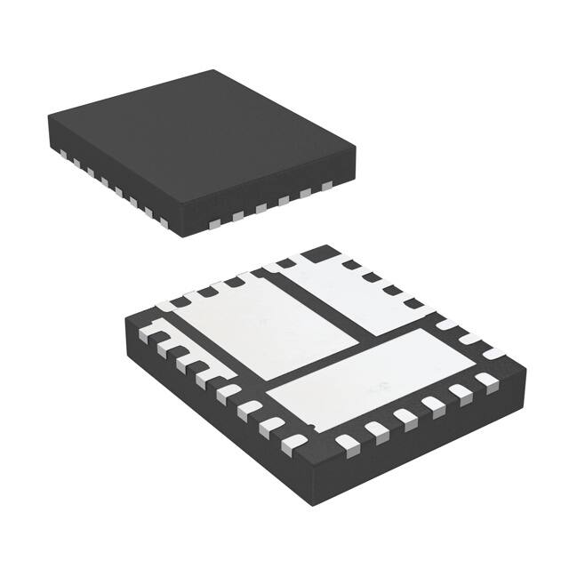
Package Type
MIC261201
28-Lead 5 mm x 6 mm VQFN (JL)
(Top View)
DS20006660A-page 1
�MIC261201
Typical Application Circuit
Functional Block Diagram
DS20006660A-page 2
2022 Microchip Technology Inc. and its subsidiaries
�MIC261201
1.0
ELECTRICAL CHARACTERISTICS
Absolute Maximum Ratings †
PVIN to PGND ............................................................................................................................................ –0.3V to +29V
VIN to PGND ............................................................................................................................................... –0.3V to PVIN
PVDD, VDD to PGND .................................................................................................................................... –0.3V to +6V
VSW, VCS to PGND ....................................................................................................................... –0.3V to (PVIN + 0.3V)
VBST to VSW ................................................................................................................................................. –0.3V to +6V
VBST to PGND............................................................................................................................................ –0.3V to +35V
VFB, VPG to PGND ......................................................................................................................... –0.3V to (VDD + 0.3V)
VEN to PGND ...................................................................................................................................–0.3V to (VIN + 0.3V)
PGND to SGND ........................................................................................................................................ –0.3V to +0.3V
Operating Ratings ‡
Supply Voltage (PVIN, VIN)......................................................................................................................... +4.5V to +28V
PVDD, VDD Supply Voltage (PVDD, VDD)................................................................................................... +4.5V to +5.5V
Enable Input (VEN) ..............................................................................................................................................0V to VIN
Maximum Power Dissipation...................................................................................................................................Note 1
† Notice: Stresses above those listed under “Absolute Maximum Ratings” may cause permanent damage to the device.
This is a stress rating only and functional operation of the device at those or any other conditions above those indicated
in the operational sections of this specification is not intended. Exposure to maximum rating conditions for extended
periods may affect device reliability. Devices are ESD sensitive. Handling precautions recommended. Human body
model, 1.5 kΩ in series with 100 pF.
‡ Notice: The device is not guaranteed to function outside its operating ratings.
Note 1: PD(MAX) = (TJ(MAX) – TA)/θJA, where θJA depends upon the printed circuit layout. A 5 square inch 4 layer,
0.62”, FR-4 PCB with 2 oz. finish copper weight per layer is used for the θJA.
ELECTRICAL CHARACTERISTICS
Electrical Characteristics: PVIN = VIN = VEN = 12V, VBST – VSW = 5V; TA = +25°C, unless noted. Bold values valid
for –40°C ≤ TJ ≤ +125°C. (Note 1)
Parameter
Symbol
Min.
Typ.
Max.
Units
Conditions
VIN,
PVIN
4.5
—
28
V
—
Quiescent Supply Current
IQ
—
730
1500
µA
ISHDN
—
5
10
VFB = 1.5V (non-switching)
Shutdown Supply Current
µA
VEN = 0V
VOUT
4.8
5
5.4
V
VIN = 7V to 28V, IDD = 40 mA
Power Supply Input
Input Voltage Range
VDD Supply Voltage
VDD Output Voltage
VDD UVLO Threshold
UVLOTH
3.7
4.2
4.5
V
VDD UVLO Hysteresis
UVLOHYS
—
400
—
mV
—
VDO
—
380
600
mV
(VIN – VDD), IDD = 25 mA
VOUT
0.8
—
5.5
V
0.792
0.8
0.808
0.788
0.8
0.812
Dropout Voltage
DC/DC Controller
Output-Voltage Adjust Range
Reference
Feedback Voltage
VFB
V
VDD Rising
—
0°C ≤ TJ ≤ +85°C (±1.5%)
–40°C ≤ TJ ≤ +125°C (±2.0%)
Load Regulation
—
—
0.25
—
%
IOUT = 0A to 12A (Continuous
Mode)
Line Regulation
—
—
0.25
—
%
VIN = 4.5V to 28V
2022 Microchip Technology Inc. and its subsidiaries
DS20006660A-page 3
�MIC261201
ELECTRICAL CHARACTERISTICS (CONTINUED)
Electrical Characteristics: PVIN = VIN = VEN = 12V, VBST – VSW = 5V; TA = +25°C, unless noted. Bold values valid
for –40°C ≤ TJ ≤ +125°C. (Note 1)
Parameter
FB Bias Current
Enable Control
Symbol
Min.
Typ.
Max.
Units
IFB
—
50
—
nA
Conditions
VFB = 0.8V
EN Logic Level High
—
1.8
—
—
V
—
EN Logic Level Low
—
—
—
0.6
V
—
EN Bias Current
IEN
—
6
30
µA
VEN = 12V
Switching Frequency
fSW
450
600
750
kHz
Maximum Duty Cycle
DCMAX
—
82
—
%
Note 3, VFB = 1.0V
Oscillator
Minimum Duty Cycle
Minimum Off-Time
Soft-Start
Soft-Start Time
Short-Circuit Protection
Current Limit Threshold
Short-Circuit Current
Internal FETs
Top MOSFET RDS(ON)
Note 2, VFB = 0V
DCMIN
—
0
—
%
—
tOFF(MIN)
—
300
—
ns
—
tSS
—
5
—
ms
—
18.75
26
37
A
VFB = 0.8V, TJ = +25°C
ILIM(TH)
17.36
26
37
A
VFB = 0.8V, TJ = +125°C
ISC
—
6
—
A
VFB = 0V
—
—
13
—
mΩ
ISW = 3A
Bottom MOSFET RDS(ON)
—
—
5.3
—
mΩ
—
—
—
60
ISW = 3A
SW Leakage Current
µA
VIN Leakage Current
—
—
—
25
VEN = 0V
µA
VEN = 0V
Power Good (PG)
PG Threshold Voltage
—
85
92
95
%VOUT Sweep VFB from Low to High
PG Hysteresis
—
—
5.5
—
%VOUT Sweep VFB from High to Low
PG Delay Time
—
—
100
—
µs
Sweep VFB from Low to High
—
—
70
200
mV
Sweep VFB < 0.9 x VNOM,
IPG = 1 mA
Overtemperature Shutdown
—
—
160
—
°C
TJ rising
Overtemperature Shutdown
Hysteresis
—
—
15
—
°C
—
PG Low Voltage
Thermal Protection
Note 1:
2:
3:
Specifications are for packaged products only.
Measured in test mode.
The maximum duty cycle is limited by the fixed mandatory off-time (tOFF) of typically 300 ns.
DS20006660A-page 4
2022 Microchip Technology Inc. and its subsidiaries
�MIC261201
TEMPERATURE SPECIFICATIONS
Parameters
Sym.
Min.
Typ.
Max.
Units
TJ(MAX)
—
—
+150
°C
Conditions
Temperature Ranges
Max. Junction Temperature
Storage Temperature Range
Lead Temperature
Junction Temperature Range
Package Thermal Resistances
Thermal Resistance, VQFN 28-Ld
Note 1:
—
TS
–65
—
+150
°C
—
TLEAD
—
—
+260
°C
Soldering, 10 sec.
TJ
–40
—
+125
°C
—
JA
—
28
—
°C/W
—
The maximum allowable power dissipation is a function of ambient temperature, the maximum allowable
junction temperature and the thermal resistance from junction to air (i.e., TA, TJ, JA). Exceeding the
maximum allowable power dissipation will cause the device operating junction temperature to exceed the
maximum +125°C rating. Sustained junction temperatures above +125°C can impact the device reliability.
2022 Microchip Technology Inc. and its subsidiaries
DS20006660A-page 5
�MIC261201
2.0
TYPICAL PERFORMANCE CURVES
Note:
The graphs and tables provided following this note are a statistical summary based on a limited number of
samples and are provided for informational purposes only. The performance characteristics listed herein
are not tested or guaranteed. In some graphs or tables, the data presented may be outside the specified
operating range (e.g., outside specified power supply range) and therefore outside the warranted range.
0.808
FEEDBACK VOLTAGE (V)
SUPPLY CURRENT (mA)
30
25
20
15
VOUT = 1.8V
IOUT = 0A
SWITCHING
10
5
0.804
0.800
0.796
VOUT = 1.8V
IOUT = 0A
0.792
0
4
10
16
22
4
28
10
FIGURE 2-1:
VIN Operating Supply
Current vs. Input Voltage.
FIGURE 2-4:
Voltage.
VEN = 0V
TOTAL REGULATION (%)
SHUTDOWN CURRENT (μA)
22
28
Feedback Voltage vs. Input
1.0%
60
REN = Open
45
30
15
VOUT = 1.8V
IOUT = 0A to 12A
0.5%
0.0%
-0.5%
-1.0%
0
4
10
16
22
4
28
10
INPUT VOLTAGE (V)
FIGURE 2-2:
Input Voltage.
16
22
28
INPUT VOLTAGE (V)
VIN Shutdown Current vs.
FIGURE 2-5:
Voltage.
10
Total Regulation vs. Input
30
25
CURRENT LIMIT (A)
8
VDD VOLTAGE (V)
16
INPUT VOLTAGE (V)
INPUT VOLTAGE (V)
6
4
VFB = 0.9V
2
IDD = 10mA
20
15
10
VOUT = 1.8V
5
0
0
4
10
16
22
28
4
FIGURE 2-3:
Input Voltage.
DS20006660A-page 6
VDD Output Voltage vs.
10
16
22
28
INPUT VOLTAGE (V)
INPUT VOLTAGE (V)
FIGURE 2-6:
Voltage.
Current Limit vs. Input
2022 Microchip Technology Inc. and its subsidiaries
�MIC261201
700
SUPPLY CURRENT (mA)
40
FREQUENCY (kHz)
650
VOUT = 1.8V
IOUT = 0A
600
550
30
20
VIN = 12V
VOUT = 1.8V
IOUT = 0A
SWITCHING
10
500
0
4
10
16
22
28
-50
-25
FIGURE 2-7:
Input Voltage.
Switching Frequency vs.
25
50
75
100
125
FIGURE 2-10:
VIN Operating Supply
Current vs. Temperature.
10
16
VEN = VIN
SUPPLY CURRENT (uA)
EN INPUT CURRENT (μA)
0
TEMPERATURE (°C)
INPUT VOLTAGE (V)
12
8
4
8
6
4
VIN = 12V
IOUT = 0A
2
VEN = 0V
0
0
4
10
16
22
28
-50
-25
FIGURE 2-8:
Input Voltage.
0
25
50
75
100
125
TEMPERATURE (°C)
INPUT VOLTAGE (V)
Enable Input Current vs.
FIGURE 2-11:
Temperature.
VIN Shutdown Current vs.
5
100%
VDD THRESHOLD (V)
VPG THRESHOLD/VREF (%)
Rising
95%
90%
85%
4
Falling
3
2
1
Hyst
VREF = 0.7V
0
80%
4
10
16
22
28
-50
FIGURE 2-9:
vs. Input Voltage.
PG Threshold/VREF Ratio
2022 Microchip Technology Inc. and its subsidiaries
-25
0
25
50
75
100
125
TEMPERATURE (°C)
INPUT VOLTAGE (V)
FIGURE 2-12:
Temperature.
VDD UVLO Threshold vs.
DS20006660A-page 7
�MIC261201
700
VIN = 12V
V IN = 12V
VOUT = 1.8V
V OUT = 1.8V
0.804
650
IOUT = 0A
FREQUENCY (kHz)
FEEBACK VOLTAGE (V)
0.808
0.800
0.796
0.792
IOUT = 0A
600
550
500
-50
-25
0
25
50
75
100
125
-50
-25
0
TEMPERATURE (°C)
Feedback Voltage vs.
FIGURE 2-16:
Temperature.
0.4%
6
0.2%
5
VDD (V)
LOAD REGULATION (%)
FIGURE 2-13:
Temperature.
25
0.0%
100
125
4
VIN = 12V
3
VOUT = 1.8V
VOUT = 1.8V
IOUT =0A to 12A
IOUT =0A
2
-0.4%
-50
-25
0
25
50
75
100
-50
125
-25
FIGURE 2-14:
Temperature.
0
25
50
75
100
125
TEMPERATURE (°C)
TEMPERATURE (°C)
Load Regulation vs.
FIGURE 2-17:
VDD vs. Temperature.
30
0.2%
25
CURRENT LIMIT (A)
LINE REGULATION (%)
75
Switching Frequency vs.
VIN = 12V
-0.2%
50
TEMPERATURE (°C)
0.1%
0.0%
V IN = 4.5V to
28V
V OUT = 1.8V
-0.1%
20
15
10
VIN = 12V
VOUT = 1.8V
5
0
-0.2%
-50
-25
0
25
50
75
100
125
-50
FIGURE 2-15:
Temperature.
DS20006660A-page 8
Line Regulation vs.
-25
0
25
50
75
100
125
TEMPERATURE (°C)
TEMPERATURE (°C)
FIGURE 2-18:
Temperature.
Current Limit vs.
2022 Microchip Technology Inc. and its subsidiaries
�MIC261201
100
1.0%
VIN = 4.5V to 28V
EFFICIENCY (%)
LINE REGULATION (%)
12VIN
90
80
24VIN
70
VOUT = 1.8V
60
VOUT = 1.8V
0.5%
0.0%
-0.5%
-1.0%
50
0
2
4
6
8
10
0
12
2
Efficiency vs. Output
FIGURE 2-22:
Current.
0.808
700
0.804
650
0.800
0.796
8
10
12
Line Regulation vs. Output
VIN = 12V
VOUT = 1.8V
600
550
VOUT = 1.8V
500
0.792
0
2
4
6
8
10
0
12
2
4
FIGURE 2-20:
Output Current.
6
8
10
12
OUTPUT CURRENT (A)
OUTPUT CURRENT (A)
Feedback Voltage vs.
FIGURE 2-23:
Output Current.
Switching Frequency vs.
5.0
1.819
VIN = 5V
1.814
VIN = 12V
OUTPUT VOLTAGE (V)
OUTPUT VOLTAGE (V)
6
VIN = 12V
FREQUENCY (kHz)
FEEDBACK VOLTAGE (V)
FIGURE 2-19:
Current.
4
OUTPUT CURRENT (A)
OUTPUT CURRENT (A)
VOUT = 1.8V
1.810
1.805
1.800
1.796
1.791
VFB < 0.8V
4.6
4.2
TA
25ºC
85ºC
125ºC
3.8
3.4
1.787
3.0
1.782
0
2
4
6
8
10
12
OUTPUT CURRENT (A)
FIGURE 2-21:
Current.
Output Voltage vs. Output
2022 Microchip Technology Inc. and its subsidiaries
0
3
6
9
12
15
OUTPUT CURRENT (A)
FIGURE 2-24:
Output Voltage (VIN = 5V)
vs. Output Current.
DS20006660A-page 9
�MIC261201
100
100
95
95
3.3V
2.5V
1.8V
1.5V
1.2V
1.0V
0.9V
0.8V
85
80
75
70
65
VIN = 5V
60
5.0V
3.3V
2.5V
1.8V
1.5V
1.2V
1.0V
0.9V
0.8V
90
EFFICIENCY (%)
EFFICIENCY (%)
90
85
80
75
70
65
60
55
VIN = 12V
55
50
50
0
3
6
9
12
0
15
3
FIGURE 2-25:
Output Current.
Efficiency (VIN = 5V) vs.
FIGURE 2-28:
Output Current.
VIN = 5V
VOUT = 0.8,V, 1.0V, 1.2V, 1.5V, 1.8V,2.5V, 3.3V
3.5
POWER DISSIPATION (W)
POWER DISSIPATION (W)
9
12
15
Efficiency (VIN = 12V) vs.
4.5
4.0
3.0
2.5
2.0
3.3V
1.5
0.8V
1.0
0.5
VIN = 12V
VOUT = 0.8,V, 1.0V, 1.2V, 1.5V, 1.8V,2.5V, 3.3V, 5.0V
4.0
3.5
3.0
2.5
2.0
5.0V
1.5
0.8V
1.0
0.5
0.0
0.0
0
3
6
0
12
9
3
6
12
9
OUTPUT CURRENT (A)
OUTPUT CURRENT (A)
FIGURE 2-26:
IC Power Dissipation (VIN =
5V) vs. Output Current.
FIGURE 2-29:
IC Power Dissipation (VIN =
12V) vs. Output Current.
100
DIE TEMPERATURE (°C)
100
DIE TEMPERATURE (°C)
6
OUTPUT CURRENT (A)
OUTPUT CURRENT (A)
80
60
40
VIN = 5V
VOUT = 1.8V
20
80
60
40
VIN = 12V
VOUT = 1.8V
20
0
0
0
2
4
6
8
10
12
OUTPUT CURRENT (A)
FIGURE 2-27:
Die Temperature* (VIN = 5V)
vs. Output Current.
0
2
4
6
8
10
12
OUTPUT CURRENT (A)
FIGURE 2-30:
Die Temperature* (VIN =
12V) vs. Output Current.
Die Temperature*: The temperature measurement was taken at the hottest point on the MIC261201 case mounted on
a 5 square inch 4 layer, 0.62”, FR-4 PCB with 2 oz. finish copper weight per layer, see Thermal Measurement section.
Actual results will depend upon the size of the PCB, ambient temperature and proximity to other heat emitting
components.
DS20006660A-page 10
2022 Microchip Technology Inc. and its subsidiaries
�MIC261201
18
90
5.0V
85
3.3V
2.5V
1.8V
1.5V
80
75
16
OUTPUT CURRENT (A)
EFFICIENCY (%)
95
1.2V
1.0V
0.9V
0.8V
70
65
60
VIN = 24V
55
0.8V
14
12
1.5V
10
8
6
V IN = 5V
4
V OUT = 0.8, 1.2, 1.5V
2
0
50
0
3
6
9
12
-50
15
FIGURE 2-31:
Output Current.
Efficiency (VIN = 24V) vs.
25
50
75
100
125
18
VIN = 24V
16
VOUT = 0.8,V, 1.0V, 1.2V, 1.5V, 1.8V,2.5V, 3.3V, 5.0V
6
OUTPUT CURRENT (A)
POWER DISSIPATION (W)
0
FIGURE 2-34:
Thermal Derating* vs.
Ambient Temperature.
7
5
4
3
5.0V
0.8V
2
1
1.8V
14
12
3.3V
10
8
6
VIN = 5V
4
VOUT = 1.8, 2.5, 3.3V
2
0
0
0
3
6
9
-50
12
-25
0
25
50
75
100
125
AMBIENT TEMPERATURE (°C)
OUTPUT CURRENT (A)
FIGURE 2-32:
IC Power Dissipation (VIN =
24V) vs. Output Current.
FIGURE 2-35:
Thermal Derating* vs.
Ambient Temperature.
18
140
16
120
OUTPUT CURRENT (A)
DIE TEMPERATURE (°C)
-25
AMBIENT TEMPERATURE (°C)
OUTPUT CURRENT (A)
100
80
60
VIN = 24V
40
VOUT = 1.8V
20
0.8V
14
12
1.8V
10
8
6
VIN = 12V
4
VOUT = 0.8, 1.2, 1.8V
2
0
0
0
2
4
6
8
10
12
OUTPUT CURRENT (A)
FIGURE 2-33:
Die Temperature* (VIN =
24V) vs. Output Current.
2022 Microchip Technology Inc. and its subsidiaries
-50
-25
0
25
50
75
100
125
AMBIENT TEMPERATURE (°C)
FIGURE 2-36:
Thermal Derating* vs.
Ambient Temperature.
DS20006660A-page 11
�MIC261201
18
OUTPUT CURRENT (A)
16
2.5V
14
12
5V
10
8
6
V IN = 12V
4
V OUT = 2.5, 3.3, 5V
2
0
-50
-25
0
25
50
75
100
125
AMBIENT TEMPERATURE (°C)
FIGURE 2-37:
Thermal Derating* vs.
Ambient Temperature.
FIGURE 2-40:
VIN Soft Turn-Off.
FIGURE 2-41:
Enable Turn-On/Turn-Off.
18
OUTPUT CURRENT (A)
16
14
12
0.8V
10
8
2.5V
6
4
VIN = 24V
2
VOUT = 0.8, 1.2, 2.5V
0
-50
-25
0
25
50
75
100
125
AMBIENT TEMPERATURE (°C)
FIGURE 2-38:
Thermal Derating* vs.
Ambient Temperature.
VOUT
FIGURE 2-39:
DS20006660A-page 12
VIN Soft Turn-On.
FIGURE 2-42:
Fall Time.
Enable Turn-Off Delay and
2022 Microchip Technology Inc. and its subsidiaries
�MIC261201
FIGURE 2-43:
VIN Start-Up with
Pre-Biased Output.
FIGURE 2-46:
VIN UVLO Thresholds.
FIGURE 2-44:
Enable Turn-On/Turn-Off.
FIGURE 2-47:
Power Up into Short Circuit.
FIGURE 2-45:
Enable Thresholds.
FIGURE 2-48:
Enabled into Short.
2022 Microchip Technology Inc. and its subsidiaries
DS20006660A-page 13
�MIC261201
FIGURE 2-49:
Short Circuit.
FIGURE 2-52:
Output Recovery from
Thermal Shutdown.
FIGURE 2-50:
Circuit.
Output Recovery from Short
FIGURE 2-53:
Switching Waveforms.
FIGURE 2-51:
Threshold.
Peak Current Limit
FIGURE 2-54:
IOUT = 0A.
Switching Waveforms;
DS20006660A-page 14
2022 Microchip Technology Inc. and its subsidiaries
�MIC261201
FIGURE 2-55:
Transient Response.
2022 Microchip Technology Inc. and its subsidiaries
DS20006660A-page 15
�MIC261201
3.0
PIN DESCRIPTIONS
The descriptions of the pins are listed in Table 3-1.
TABLE 3-1:
Pin Number
PIN FUNCTION TABLE
Pin Name
Description
1
PVDD
5V Internal Linear Regulator (Output): PVDD supply is the power MOSFET gate drive
supply voltage and created by internal LDO from VIN. When VIN < +5.5V, PVDD
should be tied to the PVIN pins. A 2.2 µF ceramic capacitor from the PVDD pin to
PGND (Pin 2) must be place next to the IC.
3
NC
No connect.
4, 9, 10, 11, 12
SW
Switch Node (Output): Internal connection for the high-side MOSFET source and
low-side MOSFET drain. Due to the high-speed switching on this pin, the SW pin
should be routed away from sensitive nodes.
2, 5, 6, 7, 8, 21
PGND
Power Ground. PGND is the ground path for the MIC26903 buck converter power
stage. The PGND pins connect to the low-side N-Channel internal MOSFET gate
drive supply ground, the sources of the MOSFETs, the negative terminals of input
capacitors, and the negative terminals of output capacitors. The loop for the power
ground should be as small as possible and separate from the Signal Ground (SGND)
loop.
13, 14, 15,
16, 17, 18, 19
PVIN
High-Side N-internal MOSFET Drain Connection (Input): The PVIN operating voltage
range is from 4.5V to 28V. Input capacitors between the PVIN pins and the power
ground (PGND) are required and keep the connection short.
BST
Boost (Output): Bootstrapped voltage to the high-side N-channel MOSFET driver. A
Schottky diode is connected between the PVDD pin and the BST pin. A boost
capacitor of 0.1 μF is connected between the BST pin and the SW pin. Adding a small
resistor at the BST pin can slow down the turn-on time of high-side N-Channel
MOSFETs.
22
CS
Current Sense (Input): The CS pin senses current by monitoring the voltage across
the low-side MOSFET during the OFF-time. The current sensing is necessary for
short circuit protection. In order to sense the current accurately, connect the low-side
MOSFET drain to SW using a Kelvin connection. The CS pin is also the high-side
MOSFET’s output driver return.
23
SGND
Signal ground. SGND must be connected directly to the ground planes. Do not route
the SGND pin to the PGND Pad on the top layer, see PCB layout guidelines for
details.
24
FB
Feedback (Input): Input to the transconductance amplifier of the control loop. The FB
pin is regulated to 0.8V. A resistor divider connecting the feedback to the output is
used to adjust the desired output voltage.
25
PG
Power Good (Output): Open Drain Output. The PG pin is externally tied with a resistor
to VDD. A high output is asserted when VOUT > 92% of nominal.
26
EN
Enable (input): A logic level control of the output. The EN pin is CMOS-compatible.
Logic high = enable, logic low = shutdown. In the off state, supply current of the
device is greatly reduced (typically 5 µA). The EN pin should not be left open.
27
VIN
Power Supply Voltage (Input): Requires bypass capacitor to SGND.
VDD
5V Internal Linear Regulator (Output): VDD supply is the power MOSFET gate drive
supply voltage and the supply bus for the IC. VDD is created by internal LDO from
VIN. When VIN < +5.5V, VDD should be tied to the PVIN pins. A 1.0 µF ceramic
capacitor from the VDD pin to PGND pins must be place next to the IC.
20
28
DS20006660A-page 16
2022 Microchip Technology Inc. and its subsidiaries
�MIC261201
4.0
FUNCTIONAL DESCRIPTION
The MIC261201 is an adaptive ON-time synchronous
step-down DC/DC regulator with an internal 5V linear
regulator and a Power Good (PG) output. It is designed
to operate over a wide input voltage range from 4.5V to
28V and provides a regulated output voltage at up to 7A
of output current. An adaptive ON-time control scheme
is employed to obtain a constant switching frequency
and to simplify the control compensation. Overcurrent
protection is implemented without the use of an
external sense resistor. The device includes an internal
soft-start function which reduces the power supply
input surge current at start-up by controlling the output
voltage rise time.
4.1
Theory of Operation
The MIC261201 operates in a continuous mode as
shown in the Functional Block Diagram.
4.2
Continuous Mode
In continuous mode, the output voltage is sensed by
the MIC261201 feedback (FB) pin via the voltage
divider R1 and R2, and compared to a 0.8V reference
voltage VREF at the error comparator through a low
gain transconductance (gm) amplifier. If the feedback
voltage decreases and the output of the gm amplifier is
below 0.8V, then the error comparator will trigger the
control logic and generate an ON-time period. The
ON-time period length is predetermined by the “FIXED
tON ESTIMATION” circuitry:
EQUATION 4-1:
V OUT
t ON ESTIMATED = --------------------------------V IN 600kHz
Where:
VOUT = Output voltage.
VIN = The power stage input voltage.
At the end of the ON-time period, the internal high-side
driver turns off the high-side MOSFET and the low-side
driver turns on the low-side MOSFET. The OFF-time
period length depends upon the feedback voltage in
most cases. When the feedback voltage decreases
and the output of the gm amplifier is below 0.8V, the
ON-time period is triggered and the OFF-time period
ends. If the OFF-time period determined by the
feedback voltage is less than the minimum OFF-time
tOFF(MIN), which is about 300 ns, the MIC261201
control logic will apply the tOFF(MIN) instead. tOFF(MIN) is
required to maintain enough energy in the boost
capacitor (CBST) to drive the high-side MOSFET.
The maximum duty cycle is obtained from the 300 ns
tOFF(MIN):
EQUATION 4-2:
t S – t OFF MIN
D MAX = ---------------------------------- = 1 – 300ns
--------------tS
tS
Where:
tS = 1/600 kHz = 1.66 µs
It is not recommended to use MIC261201 with an
OFF-time close to tOFF(MIN) during steady-state
operation. Also, as VOUT increases, the internal ripple
injection will increase and reduce the line regulation
performance. Therefore, the maximum output voltage
of the MIC261201 should be limited to 5.5V and the
maximum external ripple injection should be limited to
200 mV. Please refer to the “Setting Output Voltage”
section for more details.
The actual ON-time and resulting switching frequency
will vary with the part-to-part variation in the rise and fall
times of the internal MOSFETs, the output load current,
and variations in the VDD voltage. Also, the minimum
tON results in a lower switching frequency in high VIN to
VOUT applications, such as 24V to 1.0V. The minimum
tON measured on the MIC261201 evaluation board is
about 100 ns. During load transients, the switching
frequency is changed due to the varying OFF-time.
To illustrate the control loop operation, we will analyze
both the steady-state and load transient scenarios.
Figure 4-1 shows the MIC261201 control loop timing
during steady-state operation. During steady-state, the
gm amplifier senses the feedback voltage ripple, which
is proportional to the output voltage ripple and the
inductor current ripple, to trigger the ON-time period.
The ON-time is predetermined by the tON estimator.
The termination of the OFF-time is controlled by the
feedback voltage. At the valley of the feedback voltage
ripple, which occurs when VFB falls below VREF, the
OFF period ends and the next ON-time period is
triggered through the control logic circuitry.
FIGURE 4-1:
2022 Microchip Technology Inc. and its subsidiaries
Control Loop Timing.
DS20006660A-page 17
�MIC261201
Figure 4-2 shows the operation of the MIC261201
during a load transient. The output voltage drops due to
the sudden load increase, which causes the VFB to be
less than VREF. This will cause the error comparator to
trigger an ON-time period. At the end of the ON-time
period, a minimum OFF-time tOFF(MIN) is generated to
charge CBST because the feedback voltage is still
below VREF. Then, the next ON-time period is triggered
due to the low feedback voltage. Therefore, the
switching frequency changes during the load transient,
but returns to the nominal fixed frequency once the
output has stabilized at the new load current level. With
the varying duty cycle and switching frequency, the
output recovery time is fast and the output voltage
deviation is small in MIC261201 converter.
4.3
The MIC261201 provides a 5V regulated output for
input voltage VIN ranging from 5.5V to 28V. When
VIN < 5.5V, VDD should be tied to the PVIN pins to
bypass the internal linear regulator.
4.4
The MIC261201 implements an internal digital
soft-start by making the 0.8V reference voltage VREF
ramp from 0% to 100% in about 5 ms with 9.7 mV
steps. Therefore, the output voltage is controlled to
increase slowly by a stair-case VFB ramp. Once the
soft-start cycle ends, the related circuitry is disabled to
reduce current consumption. VDD must be powered up
at the same time or after VIN to make the soft-start
function correctly.
Unlike true current-mode control, the MIC261201 uses
the output voltage ripple to trigger an ON-time period.
The output voltage ripple is proportional to the inductor
current ripple if the ESR of the output capacitor is large
enough. The MIC261201 control loop has the
advantage of eliminating the need for slope
compensation.
In order to meet the stability requirements, the
MIC261201 feedback voltage ripple should be in phase
with the inductor current ripple and large enough to be
sensed by the gm amplifier and the error comparator.
The recommended feedback voltage ripple is
20 mV~100 mV. If a low-ESR output capacitor is
selected, then the feedback voltage ripple may be too
small to be sensed by the gm amplifier and the error
comparator. Also, the output voltage ripple and the
feedback voltage ripple are not necessarily in phase
with the inductor current ripple if the ESR of the output
capacitor is very low. In these cases, ripple injection is
required to ensure proper operation. Please refer to the
Ripple Injection section for more details about the
ripple injection technique.
Current Limit
The MIC261201 uses the RDS(ON) of the internal
low-side power MOSFET to sense overcurrent
conditions. This method will avoid adding cost, board
space and power losses taken by a discrete current
sense resistor. The low-side MOSFET is used because
it displays much lower parasitic oscillations during
switching than the high-side MOSFET.
In each switching cycle of the MIC261201 converter,
the inductor current is sensed by monitoring the
low-side MOSFET in the OFF period. If the peak
inductor current is greater than 26A, then the
MIC261201 turns off the high-side MOSFET and a
soft-start sequence is triggered. This mode of operation
is called “hiccup mode” and its purpose is to protect the
downstream load in case of a hard short. The load
current-limit threshold has a fold back characteristic
related to the feedback voltage as shown in Figure 4-3.
30
CURRENT LIMIT THRESHOLD (A)
Load Transient Response.
Soft-Start
Soft-start reduces the power supply input surge current
at startup by controlling the output voltage rise time.
The input surge appears while the output capacitor is
charged up. A slower output rise time will draw a lower
input surge current.
4.5
FIGURE 4-2:
VDD Regulator
25
20
15
10
5
0
0.0
0.2
0.4
0.6
0.8
1.0
FEEDBACK VOLTAGE (V)
FIGURE 4-3:
Characteristic.
DS20006660A-page 18
Current-Limit Foldback
2022 Microchip Technology Inc. and its subsidiaries
�MIC261201
4.6
Power Good (PG)
The Power Good (PG) pin is an open-drain output that
indicates logic high when the output is nominally 92%
of its steady state voltage. A pull-up resistor of more
than 10 kΩ should be connected from PG to VDD.
4.7
MOSFET Gate Drive
The Functional Block Diagram shows a bootstrap
circuit, consisting of D1 (a Schottky diode is
recommended) and CBST. This circuit supplies energy
to the high-side drive circuit. Capacitor CBST is
charged, while the low-side MOSFET is on, and the
voltage on the SW pin is approximately 0V. When the
high-side MOSFET driver is turned on, energy from
CBST is used to turn the MOSFET on. As the high-side
MOSFET turns on, the voltage on the SW pin increases
to approximately VIN. Diode D1 is reverse-biased and
CBST floats high while continuing to keep the high-side
MOSFET on. The bias current of the high-side driver is
less than 10 mA, so a 0.1 μF to 1 μF is sufficient to hold
the gate voltage with minimal droop for the power
stroke
(high-side
switching)
cycle,
i.e.
ΔBST = 10 mA x 1.67 μs/0.1 μF = 167 mV. When the
low-side MOSFET is turned back on, CBST is
recharged through D1.
A small resistor RG, which is in series with CBST, can be
used to slow down the turn-on time of the high-side
N-channel MOSFET.
The drive voltage is derived from the VDD supply
voltage. The nominal low-side gate drive voltage is VDD
and the nominal high-side gate drive voltage is
approximately VDD – VDIODE, where VDIODE is the
voltage drop across D1. An approximate 30 ns delay
between the high-side and low-side driver transitions is
used to prevent current from simultaneously flowing
unimpeded through both MOSFETs.
2022 Microchip Technology Inc. and its subsidiaries
DS20006660A-page 19
�MIC261201
5.0
APPLICATIONS INFORMATION
5.1
Inductor Selection
Values for inductance, peak, and RMS currents are
required to select the output inductor. The input and
output voltages and the inductance value determine
the peak-to-peak inductor ripple current. Generally,
higher inductance values are used with higher input
voltages. Larger peak-to-peak ripple currents will
increase the power dissipation in the inductor and
MOSFETs. Larger output ripple currents will also
require more output capacitance to smooth out the
larger ripple current. Smaller peak-to-peak ripple
currents require a larger inductance value and
therefore a larger and more expensive inductor. A good
compromise between size, loss and cost is to set the
inductor ripple current to be equal to 20% of the
maximum output current. The inductance value is
calculated by Equation 5-1:
EQUATION 5-1:
V OUT V IN MAX – V OUT
L = --------------------------------------------------------------------------------------V IN MAX f SW 20% I OUT MAX
Where:
fSW = Switching frequency of 600 kHz
20% = Ratio of AC ripple to DC output current
VIN(MAX) = Max. power stage input voltage
The peak-to-peak inductor current ripple is:
The RMS inductor current is used to calculate the I2R
losses in the inductor.
EQUATION 5-4:
2
I L RMS =
2 I L PP
I OUT MAX + -------------------12
Maximizing efficiency requires the proper selection of
core material and minimizing the winding resistance.
The high frequency operation of the MIC261201
requires the use of ferrite materials for all but the most
cost sensitive applications. Lower cost iron powder
cores may be used but the increase in core loss will
reduce the efficiency of the power supply. This is
especially noticeable at low output power. The winding
resistance decreases efficiency at the higher output
current levels. The winding resistance must be
minimized although this usually comes at the expense
of a larger inductor. The power dissipated in the
inductor is equal to the sum of the core and copper
losses. At higher output loads, the core losses are
usually insignificant and can be ignored. At lower
output currents, the core losses can be a significant
contributor. Core loss information is usually available
from the magnetics vendor. Copper loss in the inductor
is calculated by Equation 5-5:
EQUATION 5-5:
EQUATION 5-2:
2
V OUT V IN MAX – V OUT
I L PP = ------------------------------------------------------------------V IN MAX f SW L
The peak inductor current is equal to the average
output current plus one half of the peak-to-peak
inductor current ripple.
EQUATION 5-3:
I L PK = I OUT MAX + 0.5 I L PP
DS20006660A-page 20
P INDUCTOR CU = I L RMS R WINDING
The resistance of the copper wire, RWINDING, increases
with the temperature. The value of the winding
resistance used should be at the operating
temperature.
EQUATION 5-6:
P WINDING HT = R WINDING 20C
1 + 0.0042 T H – T 20C
Where:
TH = Temperature of wire under full load
T20°C = Ambient temperature
RWINDING(20°C) = Room temperature winding
resistance (usually specified by the manufacturer)
2022 Microchip Technology Inc. and its subsidiaries
�MIC261201
5.2
Output Capacitor Selection
The type of the output capacitor is usually determined
by its equivalent series resistance (ESR). Voltage and
RMS current capability are two other important factors
for selecting the output capacitor. Recommended
capacitor types are ceramic, low-ESR aluminum
electrolytic, OS-CON and POSCAP. The output
capacitor’s ESR is usually the main cause of the output
ripple. The output capacitor ESR also affects the
control loop from a stability point of view.
EQUATION 5-9:
I L PP
I COUT RMS = ----------------12
The power dissipated in the output capacitor is:
EQUATION 5-10:
2
P DISS COUT = I COUT RMS ESR COUT
The maximum value of ESR is calculated:
EQUATION 5-7:
V OUT PP
ESR COUT --------------------------I L PP
Where:
ΔVOUT(PP) = Peak-to-peak output voltage ripple
ΔIL(PP) = Peak-to-peak inductor current ripple
The total output ripple is a combination of the ESR and
output capacitance. The total ripple is calculated in
Equation 5-8:
EQUATION 5-8:
V OUT PP =
2
I L PP
------------------------------------- + I L PP ESR COUT 2
C OUT f SW 8
Where:
COUT = Output capacitance value
fSW = Switching frequency
As described in the Theory of Operation section, the
MIC261201 requires at least 20 mV peak-to-peak
ripple at the FB pin to make the gm amplifier and the
error comparator behave properly. Also, the output
voltage ripple should be in phase with the inductor
current. Therefore, the output voltage ripple caused by
the output capacitors value should be much smaller
than the ripple caused by the output capacitor ESR. If
low-ESR capacitors, such as ceramic capacitors, are
selected as the output capacitors, a ripple injection
method should be applied to provide the enough
feedback voltage ripple. Please refer to the Ripple
Injection section for more details.
The voltage rating of the capacitor should be twice the
output voltage for a tantalum and 20% greater for
aluminum electrolytic or OS-CON. The output capacitor
RMS current is calculated in Equation 5-9:
2022 Microchip Technology Inc. and its subsidiaries
5.3
Input Capacitor Selection
The input capacitor for the power stage input VIN
should be selected for ripple current rating and voltage
rating. Tantalum input capacitors may fail when
subjected to high inrush currents, caused by turning the
input supply on. A tantalum input capacitor’s voltage
rating should be at least two times the maximum input
voltage to maximize reliability. Aluminum electrolytic,
OS-CON, and multilayer polymer film capacitors can
handle the higher inrush currents without voltage
derating. The input voltage ripple will primarily depend
on the input capacitor’s ESR. The peak input current is
equal to the peak inductor current, so:
EQUATION 5-11:
V IN = I L PK ESR CIN
The input capacitor must be rated for the input current
ripple. The RMS value of input capacitor current is
determined at the maximum output current. Assuming
the peak-to-peak inductor current ripple is low:
EQUATION 5-12:
I CIN RMS I OUT MAX D 1 – D
The power dissipated in the input capacitor is:
EQUATION 5-13:
2
P DISS CIN = I CIN RMS ESR CIN
DS20006660A-page 21
�MIC261201
5.4
Ripple Injection
The VFB ripple required for proper operation of the
MIC261201 gm amplifier and error comparator is
20 mV to 100 mV. However, the output voltage ripple is
generally designed as 1% to 2% of the output voltage.
For a low output voltage, such as a 1V, the output
voltage ripple is only 10 mV to 20 mV, and the feedback
voltage ripple is less than 20 mV. If the feedback
voltage ripple is so small that the gm amplifier and error
comparator can’t sense it, then the MIC261201 will lose
control and the output voltage is not regulated. In order
to have some amount of VFB ripple, a ripple injection
method is applied for low output voltage ripple
applications.
The applications are divided into three situations
according to the amount of the feedback voltage ripple:
1.
Enough ripple at the feedback voltage due to the
large ESR of the output capacitors.
As shown in Figure 5-1, the converter is stable without
any ripple injection.
2.
Inadequate ripple at the feedback voltage due to
the small ESR of the output capacitors.
The output voltage ripple is fed into the FB pin through
a feedforward capacitor CFF in this situation, as shown
in Figure 5-2. The typical CFF value is between 1 nF
and 100 nF.
MIC261201
FIGURE 5-2:
Inadequate Ripple at FB.
With the feedforward capacitor, the feedback voltage
ripple is very close to the output voltage ripple:
EQUATION 5-15:
V FB PP ESR I L PP
MIC261201
FIGURE 5-1:
3.
Enough Ripple at FB.
Virtually no ripple at the FB pin voltage due to
the very-low ESR of the output capacitors.
In this situation, the output voltage ripple is less than
20 mV. Therefore, additional ripple is injected into the
FB pin from the switching node SW via a resistor RINJ
and a capacitor CINJ, as shown in Figure 5-3.
The feedback voltage ripple is:
EQUATION 5-14:
R2
V FB PP = -------------------- ESR COUT I L PP
R1 + R2
MIC261201
Where:
ΔIL(PP) = Peak-to-peak inductor current ripple
FIGURE 5-3:
Invisible Ripple at FB.
The injected ripple is:
EQUATION 5-16:
1
V FB PP = V IN K DIV D 1 – D ----------------f SW
R1//R2
K DIV = ----------------------------------R INJ + R1//R2
Where:
VIN = Power stage input voltage
D = Duty cycle
fSW = Switching frequency
τ = (R1//R2//RINJ) x CFF
DS20006660A-page 22
2022 Microchip Technology Inc. and its subsidiaries
�MIC261201
In Equation 5-17 and Equation 5-18 it is assumed that
the time constant associated with CFF must be much
greater than the switching period:
The output voltage is determined by Equation 5-20:
EQUATION 5-20:
EQUATION 5-17:
1
----------------- = 1--- « 1
f SW
Where:
VFB = 0.8V
V OUT = V FB 1 + R1
-------
R2
If the voltage divider resistors R1 and R2 are in the kΩ
range, a CFF of 1 nF to 100 nF can easily satisfy the
large time constant requirements. Also, a 100 nF
injection capacitor CINJ is used in order to be
considered as short for a wide range of the
frequencies.
A typical value of R1 can be between 3 kΩ and 10 kΩ.
If R1 is too large, it may allow noise to be introduced
into the voltage feedback loop. If R1 is too small, it will
decrease the efficiency of the power supply, especially
at light loads. Once R1 is selected, R2 can be
calculated using:
The process of sizing the ripple injection resistor and
capacitors is:
EQUATION 5-21:
Step 1. Select CFF to feed all output ripples into the
feedback pin and make sure the large time constant
assumption is satisfied. Typical choice of CFF is 1 nF to
100 nF if R1 and R2 are in the kΩ range.
Step 2. Select RINJ according to the expected feedback
voltage ripple using Equation 5-19:
EQUATION 5-18:
f SW
V FB PP
K DIV = ----------------------- ---------------------------V IN
D 1 – D
Then the value of RINJ is obtained by:
V FB R1
R2 = ----------------------------V OUT – V FB
In addition to the external ripple injection added at the
FB pin, internal ripple injection is added at the inverting
input of the comparator inside the MIC261201, as
shown in Figure 5-5. The inverting input voltage VINJ is
clamped to 1.2V. As VOUT is increased, the swing of
VINJ will be clamped. The clamped VINJ reduces the
line regulation because it is reflected as a DC error on
the FB terminal. Therefore, the maximum output
voltage of the MIC261201 should be limited to 5.5V to
avoid this problem.
EQUATION 5-19:
1 - – 1
R INJ = R1//R2 ----------K
DIV
Step 3. Select CINJ as 100 nF, which could be
considered as short for a wide range of the
frequencies.
5.5
Setting Output Voltage
The MIC261201 requires two resistors to set the output
voltage as shown in Figure 5-4.
FIGURE 5-5:
5.6
FIGURE 5-4:
Configuration.
Voltage Divider
2022 Microchip Technology Inc. and its subsidiaries
Internal Ripple Injection.
Thermal Measurements
Measuring the IC’s case temperature is recommended
to insure it is within its operating limits. Although this
might seem like a very elementary task, it is easy to get
erroneous results. The most common mistake is to use
the standard thermal couple that comes with a thermal
meter. This thermal couple wire gauge is large, typically
22 gauge, and behaves like a heatsink, resulting in a
lower case measurement.
DS20006660A-page 23
�MIC261201
Two methods of temperature measurement are using a
smaller thermal couple wire or an infrared
thermometer. If a thermal couple wire is used, it must
be constructed of 36 gauge wire or higher then (smaller
wire size) to minimize the wire heat-sinking effect. In
addition, the thermal couple tip must be covered in
either thermal grease or thermal glue to make sure that
the thermal couple junction is making good contact with
the case of the IC. Omega brand thermal couple
(5SC-TT-K-36-36) is adequate for most applications.
Wherever possible, an infrared thermometer is
recommended. The measurement spot size of most
infrared thermometers is too large for an accurate
reading on a small form factor ICs. However, a IR
thermometer from Optris has a 1 mm spot size, which
makes it a good choice for measuring the hottest point
on the case. An optional stand makes it easy to hold the
beam on the IC for long periods of time.
DS20006660A-page 24
2022 Microchip Technology Inc. and its subsidiaries
�MIC261201
6.0
PCB LAYOUT GUIDLINES
To minimize EMI and output noise, follow these layout
recommendations.
PCB Layout is critical to achieve reliable, stable and
efficient performance. A ground plane is required to
control EMI and minimize the inductance in power,
signal and return paths.
The following guidelines should be followed to insure
proper operation of the MIC261201 regulator.
6.1
IC
• A 2.2 µF ceramic capacitor, which is connected to
the PVDD pin, must be located right at the IC. The
PVDD pin is very noise sensitive and placement
of the capacitor is very critical. Use wide traces to
connect to the PVDD and PGND pins.
• A 1.0 µF ceramic capacitor must be placed right
between VDD and the signal ground SGND. The
SGND must be connected directly to the ground
planes. Do not route the SGND pin to the PGND
Pad on the top layer.
• Place the IC close to the point-of-load (POL).
• Use fat traces to route the input and output power
lines.
• Signal and power grounds should be kept
separate and connected at only one location.
6.2
Input Capacitor
• Place the input capacitor next.
• Place the input capacitors on the same side of the
board and as close to the IC as possible.
• Keep both the PVIN pin and PGND connections
short.
• Place several vias to the ground plane close to
the input capacitor ground terminal.
• Use either X7R or X5R dielectric input capacitors.
Do not use Y5V or Z5U type capacitors.
• Do not replace the ceramic input capacitor with
any other type of capacitor. Any type of capacitor
can be placed in parallel with the input capacitor.
• If a Tantalum input capacitor is placed in parallel
with the input capacitor, it must be recommended
for switching regulator applications and the
operating voltage must be derated by 50%.
• In “Hot-Plug” applications, a Tantalum or
Electrolytic bypass capacitor must be used to limit
the over-voltage spike seen on the input supply
with power is suddenly applied.
2022 Microchip Technology Inc. and its subsidiaries
6.3
Inductor
• Keep the inductor connection to the switch node
(SW) short.
• Do not route any digital lines underneath or close
to the inductor.
• Keep the switch node (SW) away from the
feedback (FB) pin.
• The CS pin should be connected directly to the
SW pin to accurate sense the voltage across the
low-side MOSFET.
• To minimize noise, place a ground plane
underneath the inductor.
• The inductor can be placed on the opposite side
of the PCB with respect to the IC. It does not
matter whether the IC or inductor is on the top or
bottom as long as there is enough air flow to keep
the power components within their temperature
limits. The input and output capacitors must be
placed on the same side of the board as the IC.
6.4
Output Capacitor
• Use a wide trace to connect the output capacitor
ground terminal to the input capacitor ground
terminal.
• Phase margin will change as the output capacitor
value and ESR changes. Contact the factory if the
output capacitor is different from what is shown in
the BOM.
• The feedback trace should be separate from the
power trace and connected as close as possible
to the output capacitor. Sensing a long high
current load trace can degrade the DC load
regulation.
6.5
Optional RC Snubber
• Place the RC snubber on either side of the board
and as close to the SW pin as possible.
DS20006660A-page 25
�MIC261201
7.0
EVALUATION BOARD SCHEMATIC
FIGURE 7-1:
TABLE 7-1:
Item
C1
Schematic of MIC261201 Evaluation Board (J11, R13, R15 are for Testing Purposes).
BILL OF MATERIALS
Part Number
Open
12105C475KAZ2A
C2, C3
GRM32ER71H475KA88L
C3225X7R1H475K
C15
C4, C5,
C13
Open
12106D107MAT2A
GRM32ER60J107ME20L
GRM188R71A105KA61D
0603ZC105KAT2A
Murata
AVX
Murata
AVX
GRM188R71H472K
Murata
C11, C16 Open
DS20006660A-page 26
2
—
—
100 µF Ceramic Capacitor, X5R, Size 1210, 6.3V
3
0.1 µF Ceramic Capacitor, X7R, Size 0603, 50V
3
1.0 µF Ceramic Capacitor, X7R, Size 0603, 10V
1
2.2 µF Ceramic Capacitor, X7R, Size 0603, 10V
1
4.7 nF Ceramic Capacitor, X7R, Size 0603, 50V
1
220 µF Aluminum Capacitor, 35V
1
—
—
TDK
06035C472KAZ2A
B41851F7227M
4.7 µF Ceramic Capacitor, X7R, Size 1210, 50V
AVX
Murata
TDK
C1608X7R1H472K
—
TDK
C1608X7R1A105K
GRM188R61A225KE34D
—
AVX
Murata
0603ZD225KAT2A
C1608X5R1A225K
C14
—
AVX
C8
Qty.
TDK
TDK
C1608X7R1H104K
Description
AVX
Murata
06035C104KAT2A
GRM188R71H104KA93D
C12
—
C3225X5R0J107M
C6, C7,
C10
C9
Manufacturer
TDK
EPCOS
—
2022 Microchip Technology Inc. and its subsidiaries
�MIC261201
TABLE 7-1:
Item
BILL OF MATERIALS (CONTINUED)
Part Number
SD103AWS
D1
SD103AWS-7
SD103AWS
Manufacturer
Description
Qty.
MCC
Diodes, Inc.
40V, 350 mA, Schottky Diode, SOD323
1
Vishay
L1
HCF1305-1R0-R
Cooper
Bussmann
1.0 µH Inductor, 21A Saturation Current
1
R1
CRCW06032R21FKEA
Vishay Dale
2.21Ω Resistor, Size 0603, 1%
1
R2
CRCW06032R00FKEA
Vishay Dale
2.00Ω Resistor, Size 0603, 1%
1
R3
CRCW060319K6FKEA
Vishay Dale
19.6 kΩ Resistor, Size 0603, 1%
1
R4
CRCW06032K49FKEA
Vishay Dale
2.49 kΩ Resistor, Size 0603, 1%
1
R5
CRCW060320K0FKEA
Vishay Dale
20.0 kΩ Resistor, Size 0603, 1%
1
R6, R14,
CRCW060310K0FKEA
R17
Vishay Dale
10.0 kΩ Resistor, Size 0603, 1%
3
R7
CRCW06034K99FKEA
Vishay Dale
4.99 kΩ Resistor, Size 0603, 1%
1
R8
CRCW06032K87FKEA
Vishay Dale
2.87 kΩ Resistor, Size 0603, 1%
1
R9
CRCW06032K006FKEA
Vishay Dale
2.00 kΩ Resistor, Size 0603, 1%
1
R10
CRCW06031K18FKEA
Vishay Dale
1.18 kΩ Resistor, Size 0603, 1%
1
R11
CRCW0603806RFKEA
Vishay Dale
806Ω Resistor, Size 0603, 1%
1
R12
CRCW0603475RFKEA
Vishay Dale
475Ω Resistor, Size 0603, 1%
1
R13
CRCW06030000FKEA
Vishay Dale
0Ω Resistor, Size 0603, 5%
1
R15
CRCW060349R9FKEA
Vishay Dale
49.9Ω Resistor, Size 0603, 1%
1
R16, R18 CRCW06031R21FKEA
Vishay Dale
1.21Ω Resistor, Size 0603, 1%
2
—
—
R20
Open
U1
MIC261201YJL
—
Microchip
2022 Microchip Technology Inc. and its subsidiaries
28V, 12A Hyper Speed Control? Synchronous
DC/DC Buck Regulator
DS20006660A-page 27
�MIC261201
8.0
PCB EVALUATION BOARD LAYOUT
FIGURE 8-1:
Evaluation Board Top Layer.
FIGURE 8-3:
Eval. Board Mid-Layer 2.
FIGURE 8-2:
(Ground Plane).
Eval. Board Mid-Layer 1
FIGURE 8-4:
Layer.
Evaluation Board Bottom
DS20006660A-page 28
2022 Microchip Technology Inc. and its subsidiaries
�MIC261201
FIGURE 8-5:
EV Board Dimensions.
2022 Microchip Technology Inc. and its subsidiaries
DS20006660A-page 29
�MIC261201
9.0
PACKAGING INFORMATION
9.1
Package Marking Information
28-Lead VQFN*
XXX
XXXXXXXXX
WNNN
Legend: XX...X
Y
YY
WW
NNN
e3
*
Example
MIC
261201YJL
2GT7
Product code or customer-specific information
Year code (last digit of calendar year)
Year code (last 2 digits of calendar year)
Week code (week of January 1 is week ‘01’)
Alphanumeric traceability code
Pb-free JEDEC® designator for Matte Tin (Sn)
This package is Pb-free. The Pb-free JEDEC designator ( e3 )
can be found on the outer packaging for this package.
●, ▲, ▼ Pin one index is identified by a dot, delta up, or delta down (triangle
mark).
Note:
In the event the full Microchip part number cannot be marked on one line, it will
be carried over to the next line, thus limiting the number of available
characters for customer-specific information. Package may or may not include
the corporate logo.
Underbar (_) symbol may not be to scale.
Note:
If the full seven-character YYWWNNN code cannot fit on the package, the following truncated codes are
used based on the available marking space:
6 Characters = YWWNNN; 5 Characters = WWNNN; 4 Characters = WNNN; 3 Characters = NNN;
2 Characters = NN; 1 Character = N
DS20006660A-page 30
2022 Microchip Technology Inc. and its subsidiaries
�MIC261201
28-Lead VQFN 5 mm x 6 mm Package Outline and Recommended Land Pattern
28-Lead Very Thin Plastic Quad Flat, No Lead Package (PKA) - 5x6x0.9 mm Body [VQFN]
With Multiple Exposed Pads and Fused Terminals; Micrel Legacy QFN56-28LD-PL-1
Note:
For the most current package drawings, please see the Microchip Packaging Specification located at
http://www.microchip.com/packaging
2X
28X
0.05 C
D
A
0.08 C
B
N
NOTE 1
1
2
3
E
(DATUM B)
(DATUM A)
2X
0.05 C
TOP VIEW
A1
(A3)
(K3)
A
D2
D4 0.60
D3
(K4)
0.10 C
(L3)
(K2)
(L2)
E2
C
SEATING
PLANE
SIDE VIEW
E4
e
2
E5
(K4)
3
(K5)
E3
2
(K1)
1
NOTE 1
N
28X b
L1
e
D4
0.07
0.05
C A B
C
BOTTOM VIEW
Microchip Technology Drawing C04-1120 Rev A Sheet 1 of 2
2022 Microchip Technology Inc. and its subsidiaries
DS20006660A-page 31
�MIC261201
28-Lead Very Thin Plastic Quad Flat, No Lead Package (PKA) - 5x6x0.9 mm Body [VQFN]
With Multiple Exposed Pads and Fused Terminals; Micrel Legacy QFN56-28LD-PL-1
Note:
For the most current package drawings, please see the Microchip Packaging Specification located at
http://www.microchip.com/packaging
Units
Dimension Limits
Number of Terminals
N
e
Pitch
A
Overall Height
Standoff
A1
A3
Terminal Thickness
Overall Length
D
Exposed Pad Length
D2
D3
Exposed Pad Length
Exposed Pad Length
D4
Overall Width
E
E2
Exposed Pad Width
Exposed Pad Width
E3
Exposed Pad Width
E4
Exposed Pad Width
E5
b
Terminal Width
Terminal Length
L1
Terminal Length
L2
L3
Terminal Length
Terminal to Exposed Pad
K1
Body Edge to Exposed Pad
K2
K3
Exposed Pad to Exposed Pad
Exposed Pad Offset
K4
K5
Exposed Pad to Exposed Pad
MILLIMETERS
NOM
MAX
28
0.65 BSC
0.02
0.00
0.05
0.85
0.80
0.85
0.20 REF
5.00 BSC
2.15
2.20
2.25
1.35
1.40
1.45
3.65
3.70
3.75
6.00 BSC
2.95
2.90
3.00
1.575
1.60
1.625
2.40
2.50
2.45
2.85
2.90
2.95
0.30
0.25
0.35
0.40
0.35
0.45
0.45 REF
0.15 REF
0.25 REF
0.575 REF
0.035 REF
0.40 REF
0.35 REF
MIN
Notes:
1. Pin 1 visual index feature may vary, but must be located within the hatched area.
2. Package is saw singulated
3. Dimensioning and tolerancing per ASME Y14.5M
BSC: Basic Dimension. Theoretically exact value shown without tolerances.
REF: Reference Dimension, usually without tolerance, for information purposes only.
Microchip Technology Drawing C04-1120 Rev A Sheet 2 of 2
DS20006660A-page 32
2022 Microchip Technology Inc. and its subsidiaries
�MIC261201
28-Lead Very Thin Plastic Quad Flat, No Lead Package (PKA) - 5x6x0.9 mm Body [VQFN]
With Multiple Exposed Pads and Fused Terminals; Micrel Legacy QFN56-28LD-PL-1
Note:
For the most current package drawings, please see the Microchip Packaging Specification located at
http://www.microchip.com/packaging
C1
X2
EV
28
G4
1
2
Y2
G2
G3
C2
ØV
EV
Y3
G1
Y1
SILK SCREEN
E
X1
X3
G6
G5
X4
RECOMMENDED LAND PATTERN
Contact Pitch
Center Pad Width
Center Pad Width
Center Pad Width
Center Pad Length
Center Pad Length
Contact Pad Width
Contact Pad Length
Contact Pad Spacing
Units
Dimension Limits
E
X2
X3
X4
Y2
Y3
X1
Y1
C1
MILLIMETERS
MIN NOM MAX
0.65 BSC
3.70
2.20
0.90
1.60
2.83
0.30
0.40
4 .8 0
Units
Dimension Limits
Contact Pad Spacing
C2
Contact Pad to Center Pad
G1
Contact Pad to Contact Pad
G2
Center Pad to Center Pad
G3
Contact Pad to Center Pad
G4
Contact Pad to Center Pad
G5
Center Pad to Center Pad
G6
Thermal Via Diameter
V
Thermal Via Pitch
EV
MILLIMETERS
MIN NOM MAX
5.80
0.12
0.35
0.35
0.35
0.60
0.13
0.30
1.00
Notes:
1. Dimensioning and tolerancing per ASME Y14.5M
BSC: Basic Dimension. Theoretically exact value shown without tolerances.
2. For best soldering results, thermal vias, if used, should be filled or tented to avoid solder loss during
reflow process
Microchip Technology Drawing C04-3120 Rev A
2022 Microchip Technology Inc. and its subsidiaries
DS20006660A-page 33
�MIC261201
NOTES:
DS20006660A-page 34
2022 Microchip Technology Inc. and its subsidiaries
�MIC261201
APPENDIX A:
REVISION HISTORY
Revision A (April 2022)
• Converted Micrel document MIC261201 to Microchip data sheet DS20006660A.
• Minor text changes throughout.
2022 Microchip Technology Inc. and its subsidiaries
DS20006660A-page 35
�MIC261201
NOTES:
DS20006660A-page 36
2022 Microchip Technology Inc. and its subsidiaries
�MIC261201
PRODUCT IDENTIFICATION SYSTEM
To order or obtain information, e.g., on pricing or delivery, contact your local Microchip representative or sales office.
Part Number
X
XX
-XX
Device
Temp.
Range
Package
Media Type
Device:
MIC261201:
28V, 12A Hyper Speed Control® Synchronous DC/DC Buck Regulator
Temperature
Range:
Y
=
–40°C to +125°C
Package:
JL
=
28-Lead VQFN
Media Type:
TR
=
1,000/Reel
2022 Microchip Technology Inc. and its subsidiaries
Examples:
a) MIC261201YJL-TR:
Note 1:
MIC261201,
–40°C to +125°C Temp.
Range, 28-Lead VQFN,
1000/Reel
Tape and Reel identifier only appears in the
catalog part number description. This identifier is
used for ordering purposes and is not printed on
the device package. Check with your Microchip
Sales Office for package availability with the Tape
and Reel option.
DS20006660A-page 37
�MIC261201
NOTES:
DS20006660A-page 38
2022 Microchip Technology Inc. and its subsidiaries
�Note the following details of the code protection feature on Microchip products:
•
Microchip products meet the specifications contained in their particular Microchip Data Sheet.
•
Microchip believes that its family of products is secure when used in the intended manner, within operating specifications, and
under normal conditions.
•
Microchip values and aggressively protects its intellectual property rights. Attempts to breach the code protection features of
Microchip product is strictly prohibited and may violate the Digital Millennium Copyright Act.
•
Neither Microchip nor any other semiconductor manufacturer can guarantee the security of its code. Code protection does not
mean that we are guaranteeing the product is “unbreakable”. Code protection is constantly evolving. Microchip is committed to
continuously improving the code protection features of our products.
This publication and the information herein may be used only
with Microchip products, including to design, test, and integrate
Microchip products with your application. Use of this information in any other manner violates these terms. Information
regarding device applications is provided only for your convenience and may be superseded by updates. It is your responsibility to ensure that your application meets with your
specifications. Contact your local Microchip sales office for
additional support or, obtain additional support at https://
www.microchip.com/en-us/support/design-help/client-supportservices.
THIS INFORMATION IS PROVIDED BY MICROCHIP "AS IS".
MICROCHIP MAKES NO REPRESENTATIONS OR WARRANTIES OF ANY KIND WHETHER EXPRESS OR IMPLIED,
WRITTEN OR ORAL, STATUTORY OR OTHERWISE,
RELATED TO THE INFORMATION INCLUDING BUT NOT
LIMITED TO ANY IMPLIED WARRANTIES OF NONINFRINGEMENT, MERCHANTABILITY, AND FITNESS FOR A
PARTICULAR PURPOSE, OR WARRANTIES RELATED TO
ITS CONDITION, QUALITY, OR PERFORMANCE.
IN NO EVENT WILL MICROCHIP BE LIABLE FOR ANY INDIRECT, SPECIAL, PUNITIVE, INCIDENTAL, OR CONSEQUENTIAL LOSS, DAMAGE, COST, OR EXPENSE OF ANY
KIND WHATSOEVER RELATED TO THE INFORMATION OR
ITS USE, HOWEVER CAUSED, EVEN IF MICROCHIP HAS
BEEN ADVISED OF THE POSSIBILITY OR THE DAMAGES
ARE FORESEEABLE. TO THE FULLEST EXTENT
ALLOWED BY LAW, MICROCHIP'S TOTAL LIABILITY ON
ALL CLAIMS IN ANY WAY RELATED TO THE INFORMATION
OR ITS USE WILL NOT EXCEED THE AMOUNT OF FEES, IF
ANY, THAT YOU HAVE PAID DIRECTLY TO MICROCHIP
FOR THE INFORMATION.
Use of Microchip devices in life support and/or safety applications is entirely at the buyer's risk, and the buyer agrees to
defend, indemnify and hold harmless Microchip from any and
all damages, claims, suits, or expenses resulting from such
use. No licenses are conveyed, implicitly or otherwise, under
any Microchip intellectual property rights unless otherwise
stated.
Trademarks
The Microchip name and logo, the Microchip logo, Adaptec,
AnyRate, AVR, AVR logo, AVR Freaks, BesTime, BitCloud,
CryptoMemory, CryptoRF, dsPIC, flexPWR, HELDO, IGLOO,
JukeBlox, KeeLoq, Kleer, LANCheck, LinkMD, maXStylus,
maXTouch, MediaLB, megaAVR, Microsemi, Microsemi logo,
MOST, MOST logo, MPLAB, OptoLyzer, PIC, picoPower,
PICSTART, PIC32 logo, PolarFire, Prochip Designer, QTouch,
SAM-BA, SenGenuity, SpyNIC, SST, SST Logo, SuperFlash,
Symmetricom, SyncServer, Tachyon, TimeSource, tinyAVR, UNI/O,
Vectron, and XMEGA are registered trademarks of Microchip
Technology Incorporated in the U.S.A. and other countries.
AgileSwitch, APT, ClockWorks, The Embedded Control Solutions
Company, EtherSynch, Flashtec, Hyper Speed Control, HyperLight
Load, IntelliMOS, Libero, motorBench, mTouch, Powermite 3,
Precision Edge, ProASIC, ProASIC Plus, ProASIC Plus logo, QuietWire, SmartFusion, SyncWorld, Temux, TimeCesium, TimeHub,
TimePictra, TimeProvider, TrueTime, WinPath, and ZL are
registered trademarks of Microchip Technology Incorporated in the
U.S.A.
Adjacent Key Suppression, AKS, Analog-for-the-Digital Age, Any
Capacitor, AnyIn, AnyOut, Augmented Switching, BlueSky,
BodyCom, CodeGuard, CryptoAuthentication, CryptoAutomotive,
CryptoCompanion, CryptoController, dsPICDEM, dsPICDEM.net,
Dynamic Average Matching, DAM, ECAN, Espresso T1S,
EtherGREEN, GridTime, IdealBridge, In-Circuit Serial
Programming, ICSP, INICnet, Intelligent Paralleling, Inter-Chip
Connectivity, JitterBlocker, Knob-on-Display, maxCrypto, maxView,
memBrain, Mindi, MiWi, MPASM, MPF, MPLAB Certified logo,
MPLIB, MPLINK, MultiTRAK, NetDetach, NVM Express, NVMe,
Omniscient Code Generation, PICDEM, PICDEM.net, PICkit,
PICtail, PowerSmart, PureSilicon, QMatrix, REAL ICE, Ripple
Blocker, RTAX, RTG4, SAM-ICE, Serial Quad I/O, simpleMAP,
SimpliPHY, SmartBuffer, SmartHLS, SMART-I.S., storClad, SQI,
SuperSwitcher, SuperSwitcher II, Switchtec, SynchroPHY, Total
Endurance, TSHARC, USBCheck, VariSense, VectorBlox, VeriPHY,
ViewSpan, WiperLock, XpressConnect, and ZENA are trademarks
of Microchip Technology Incorporated in the U.S.A. and other
countries.
SQTP is a service mark of Microchip Technology Incorporated in
the U.S.A.
The Adaptec logo, Frequency on Demand, Silicon Storage
Technology, Symmcom, and Trusted Time are registered
trademarks of Microchip Technology Inc. in other countries.
GestIC is a registered trademark of Microchip Technology Germany
II GmbH & Co. KG, a subsidiary of Microchip Technology Inc., in
other countries.
All other trademarks mentioned herein are property of their
respective companies.
© 2022, Microchip Technology Incorporated and its subsidiaries.
All Rights Reserved.
For information regarding Microchip’s Quality Management Systems,
please visit www.microchip.com/quality.
2022 Microchip Technology Inc. and its subsidiaries
ISBN: 978-1-6683-0170-8
DS20006660A-page 39
�Worldwide Sales and Service
AMERICAS
ASIA/PACIFIC
ASIA/PACIFIC
EUROPE
Corporate Office
2355 West Chandler Blvd.
Chandler, AZ 85224-6199
Tel: 480-792-7200
Fax: 480-792-7277
Technical Support:
http://www.microchip.com/
support
Web Address:
www.microchip.com
Australia - Sydney
Tel: 61-2-9868-6733
India - Bangalore
Tel: 91-80-3090-4444
China - Beijing
Tel: 86-10-8569-7000
India - New Delhi
Tel: 91-11-4160-8631
Austria - Wels
Tel: 43-7242-2244-39
Fax: 43-7242-2244-393
China - Chengdu
Tel: 86-28-8665-5511
India - Pune
Tel: 91-20-4121-0141
China - Chongqing
Tel: 86-23-8980-9588
Japan - Osaka
Tel: 81-6-6152-7160
China - Dongguan
Tel: 86-769-8702-9880
Japan - Tokyo
Tel: 81-3-6880- 3770
China - Guangzhou
Tel: 86-20-8755-8029
Korea - Daegu
Tel: 82-53-744-4301
China - Hangzhou
Tel: 86-571-8792-8115
Korea - Seoul
Tel: 82-2-554-7200
China - Hong Kong SAR
Tel: 852-2943-5100
Malaysia - Kuala Lumpur
Tel: 60-3-7651-7906
China - Nanjing
Tel: 86-25-8473-2460
Malaysia - Penang
Tel: 60-4-227-8870
China - Qingdao
Tel: 86-532-8502-7355
Philippines - Manila
Tel: 63-2-634-9065
China - Shanghai
Tel: 86-21-3326-8000
Singapore
Tel: 65-6334-8870
China - Shenyang
Tel: 86-24-2334-2829
Taiwan - Hsin Chu
Tel: 886-3-577-8366
China - Shenzhen
Tel: 86-755-8864-2200
Taiwan - Kaohsiung
Tel: 886-7-213-7830
China - Suzhou
Tel: 86-186-6233-1526
Taiwan - Taipei
Tel: 886-2-2508-8600
China - Wuhan
Tel: 86-27-5980-5300
Thailand - Bangkok
Tel: 66-2-694-1351
China - Xian
Tel: 86-29-8833-7252
Vietnam - Ho Chi Minh
Tel: 84-28-5448-2100
Atlanta
Duluth, GA
Tel: 678-957-9614
Fax: 678-957-1455
Austin, TX
Tel: 512-257-3370
Boston
Westborough, MA
Tel: 774-760-0087
Fax: 774-760-0088
Chicago
Itasca, IL
Tel: 630-285-0071
Fax: 630-285-0075
Dallas
Addison, TX
Tel: 972-818-7423
Fax: 972-818-2924
Detroit
Novi, MI
Tel: 248-848-4000
Houston, TX
Tel: 281-894-5983
Indianapolis
Noblesville, IN
Tel: 317-773-8323
Fax: 317-773-5453
Tel: 317-536-2380
Los Angeles
Mission Viejo, CA
Tel: 949-462-9523
Fax: 949-462-9608
Tel: 951-273-7800
Raleigh, NC
Tel: 919-844-7510
New York, NY
Tel: 631-435-6000
San Jose, CA
Tel: 408-735-9110
Tel: 408-436-4270
Canada - Toronto
Tel: 905-695-1980
Fax: 905-695-2078
DS20006660A-page 40
China - Xiamen
Tel: 86-592-2388138
China - Zhuhai
Tel: 86-756-3210040
Denmark - Copenhagen
Tel: 45-4485-5910
Fax: 45-4485-2829
Finland - Espoo
Tel: 358-9-4520-820
France - Paris
Tel: 33-1-69-53-63-20
Fax: 33-1-69-30-90-79
Germany - Garching
Tel: 49-8931-9700
Germany - Haan
Tel: 49-2129-3766400
Germany - Heilbronn
Tel: 49-7131-72400
Germany - Karlsruhe
Tel: 49-721-625370
Germany - Munich
Tel: 49-89-627-144-0
Fax: 49-89-627-144-44
Germany - Rosenheim
Tel: 49-8031-354-560
Israel - Ra’anana
Tel: 972-9-744-7705
Italy - Milan
Tel: 39-0331-742611
Fax: 39-0331-466781
Italy - Padova
Tel: 39-049-7625286
Netherlands - Drunen
Tel: 31-416-690399
Fax: 31-416-690340
Norway - Trondheim
Tel: 47-7288-4388
Poland - Warsaw
Tel: 48-22-3325737
Romania - Bucharest
Tel: 40-21-407-87-50
Spain - Madrid
Tel: 34-91-708-08-90
Fax: 34-91-708-08-91
Sweden - Gothenberg
Tel: 46-31-704-60-40
Sweden - Stockholm
Tel: 46-8-5090-4654
UK - Wokingham
Tel: 44-118-921-5800
Fax: 44-118-921-5820
2022 Microchip Technology Inc. and its subsidiaries
09/14/21
�