MIC29712
7.5A Fast-Response LDO Regulator
Features
General Description
•
•
•
•
•
•
•
The MIC29712 is a high-current, high-accuracy,
low-dropout voltage regulator that features fast
transient recovery from input voltage surges and output
load current changes. This regulator uses a PNP pass
element that features Microchip’s proprietary Super
ßeta PNP process.
Fast Transient Response
7.5A Current Capability
700 mV Dropout Voltage at Full Load
Low Ground Current
Accurate 2% Guaranteed Tolerance
“Zero” Current Shutdown Mode
Adjustable Output Voltage
Applications
• Pentium®, Pentium® Plus, and Power PC®
Processor Supplies
• High-Efficiency “Green” Computer Systems
• High-Efficiency Linear Power Supplies
• High-Efficiency Switching Supply Post Regulator
• Battery-Powered Equipment
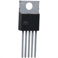
Package Type
A TTL-compatible enable (EN) control pin supports
external on/off control. If on/off control is not required,
the device may be continuously enabled by connecting
EN to IN.
The MIC29712 is available in the 5-pin TO-220
package with an operating junction temperature range
of 0°C to +125°C.
For applications that require even lower dropout
voltage or input voltage greater than 16V, see the
MIC29752.
EN
IN
GND
OUT
ADJ
MIC29712
5-Lead TO-220 (T)
(Top View)
The MIC29712 is an adjustable output voltage device.
It is fully protected against overcurrent faults, reversed
lead insertion, overtemperature operation, and positive
and negative transient voltage spikes.
2018 Microchip Technology Inc.
DS20006068A-page 1
�MIC29712
Typical Application Circuit
MIC29712
On
Off
VOUT
OUT
EN
R1
VIN
ADJ
IN
GND
R2
VOUT = 1.240(R1/R2 + 1)
Functional Block Diagram
OUT
IN
EN
On/Off
Bias
O.V.
ILIMIT
28V
16V
Reference
Feedback
ADJ
Thermal
Shutdown
GND
DS20006068A-page 2
2018 Microchip Technology Inc.
�MIC29712
1.0
ELECTRICAL CHARACTERISTICS
Absolute Maximum Ratings †
Input Supply Voltage (VIN) (Note 1) ........................................................................................................... –0.7V to +20V
Power Dissipation .................................................................................................................................. Internally Limited
Lead Temperature (Soldering, 5 sec.)................................................................................................................... +260°C
Storage Temperature (TS)...................................................................................................................... –65°C to +150°C
ESD Rating .............................................................................................................................................................Note 2
Operating Ratings ††
Junction Temperature (TJ).......................................................................................................................... 0°C to +125°C
Package Thermal Resistance
TO-220 (JC) ...........................................................................................................................................................2°C/W
TO-220 (JA) .........................................................................................................................................................55°C/W
† Notice: Stresses above those listed under “Absolute Maximum Ratings” may cause permanent damage to the device.
This is a stress rating only and functional operation of the device at those or any other conditions above those indicated
in the operational sections of this specification is not intended. Exposure to maximum rating conditions for extended
periods may affect device reliability.
†† Notice: The device is not guaranteed to function outside its operating ratings.
Note 1: The maximum continuous supply voltage is 16V.
2: Devices are ESD sensitive. Handling precautions are recommended.
ELECTRICAL CHARACTERISTICS
Electrical Characteristics: All measurements at TJ = +25°C unless otherwise noted. Bold values are guaranteed
across the operating temperature range. Note 1
Parameter
Sym.
Min.
Typ.
Max.
Units
Output Voltage
VOUT
–2
—
2
%
10 mA ≤ IOUT ≤ 7.5A,
(VOUT + 1V) ≤ VIN ≤ 8V, Note 2
Line Regulation
∆VOUT/
VOUT
—
0.06
0.5
%
IOUT = 10 mA, (VOUT + 1V) ≤ VIN ≤ 8V
Load Regulation
∆VOUT/
VOUT
—
0.2
1
%
VIN = VOUT + 1V, 10 mA ≤ IOUT ≤ 7.5A,
Note 2
Output Voltage
Temperature Coefficient
∆VOUT/
∆T
—
20
100
Note 1:
2:
3:
4:
5:
6:
7:
8:
Conditions
ppm/°C Note 4
Specification for packaged product only.
For testing, MIC29712 VOUT is programmed to 5V.
VEN ≤ 0.8V and VIN ≤ 16V, VOUT = 0.
Output voltage temperature coefficient is defined as the worst-case voltage change divided by the total
temperature range.
Dropout voltage is defined as the input-to-output differential when the output voltage drops to 99% of its
nominal value with VOUT + 1V applied to VIN.
Ground pin current is the regulator quiescent current. The total current drawn from the source is the sum
of the load current plus the ground pin current.
For this test, VIN is the larger of 8V or VOUT + 3V.
VREF ≤ VOUT ≤ (VIN – 1 V), 2.4V ≤ VIN ≤ 8V, 10 mA < IL ≤ 7.5A, TJ ≤ TJ(MAX).
2018 Microchip Technology Inc.
DS20006068A-page 3
�MIC29712
ELECTRICAL CHARACTERISTICS (CONTINUED)
Electrical Characteristics: All measurements at TJ = +25°C unless otherwise noted. Bold values are guaranteed
across the operating temperature range. Note 1
Parameter
Min.
Typ.
Max.
—
80
200
IOUT = 100 mA
—
180
—
IOUT = 750 mA
—
220
—
—
300
—
—
450
—
—
700
1000
—
6
20
IOUT = 750 mA, VIN = VOUT + 1V
—
20
—
IOUT = 1.5A
—
36
—
—
100
—
—
250
375
IGNDDO
—
1
2
mA
ILIM
—
11
15
A
en
—
260
—
Reference Voltage
VREF
1.215
1.240
1.265
Adjust Pin Bias Current
IBIAS
—
40
80
—
—
120
Reference Voltage
Temperature Coefficient
—
—
20
—
ppm/°C Note 8
Adjust Pin Bias Current
Temperature Coefficient
—
—
0.1
—
nA/°C
VIL
—
—
0.8
VIH
2.4
—
—
Dropout Voltage
∆VOUT = –1% (Note 5)
Ground Current (Note 6)
Ground Pin Current at
Dropout
Current Limit
Output Noise Voltage
10 Hz to 10 kHz
Sym.
VDO
IGND
Units
mV
Conditions
IOUT = 1.5A
IOUT = 3A
IOUT = 5A
IOUT = 7.5A
mA
IOUT = 3A
IOUT = 5A
IOUT = 7.5A
VIN = 0.5V less than specified VOUT.
IOUT = 10 mA
VOUT = 0V, Note 7
µVRMS CL = 47 µF, IOUT = 100 mA, VOUT = 5V
Reference
V
10 mA ≤ IOUT ≤ 7.5A,
(VOUT + 1V) ≤ VIN ≤ 8V, Note 2
nA
—
—
Enable Input
Input Logic Voltage
Note 1:
2:
3:
4:
5:
6:
7:
8:
V
Low (off)
High (on)
Specification for packaged product only.
For testing, MIC29712 VOUT is programmed to 5V.
VEN ≤ 0.8V and VIN ≤ 16V, VOUT = 0.
Output voltage temperature coefficient is defined as the worst-case voltage change divided by the total
temperature range.
Dropout voltage is defined as the input-to-output differential when the output voltage drops to 99% of its
nominal value with VOUT + 1V applied to VIN.
Ground pin current is the regulator quiescent current. The total current drawn from the source is the sum
of the load current plus the ground pin current.
For this test, VIN is the larger of 8V or VOUT + 3V.
VREF ≤ VOUT ≤ (VIN – 1 V), 2.4V ≤ VIN ≤ 8V, 10 mA < IL ≤ 7.5A, TJ ≤ TJ(MAX).
DS20006068A-page 4
2018 Microchip Technology Inc.
�MIC29712
ELECTRICAL CHARACTERISTICS (CONTINUED)
Electrical Characteristics: All measurements at TJ = +25°C unless otherwise noted. Bold values are guaranteed
across the operating temperature range. Note 1
Parameter
Enable Pin Input Current
Regulator Output Current
in Shutdown
Note 1:
2:
3:
4:
5:
6:
7:
8:
Sym.
IIN
—
Min.
Typ.
Max.
—
15
30
—
—
75
—
—
2
—
—
4
—
10
—
—
—
20
Units
Conditions
VEN = VIN
µA
VEN = 0.8V
µA
Note 3
Specification for packaged product only.
For testing, MIC29712 VOUT is programmed to 5V.
VEN ≤ 0.8V and VIN ≤ 16V, VOUT = 0.
Output voltage temperature coefficient is defined as the worst-case voltage change divided by the total
temperature range.
Dropout voltage is defined as the input-to-output differential when the output voltage drops to 99% of its
nominal value with VOUT + 1V applied to VIN.
Ground pin current is the regulator quiescent current. The total current drawn from the source is the sum
of the load current plus the ground pin current.
For this test, VIN is the larger of 8V or VOUT + 3V.
VREF ≤ VOUT ≤ (VIN – 1 V), 2.4V ≤ VIN ≤ 8V, 10 mA < IL ≤ 7.5A, TJ ≤ TJ(MAX).
2018 Microchip Technology Inc.
DS20006068A-page 5
�MIC29712
TEMPERATURE SPECIFICATIONS
Parameters
Sym.
Min.
Typ.
Max.
Units
Conditions
TJ
0
—
+125
°C
—
Temperature Ranges
Operating Temperature Range
Lead Temperature
—
—
—
+260
°C
Soldering, 5 sec.
Storage Temperature
TS
–65
—
+150
°C
—
Thermal Resistance, TO-220 5-Ld
JC
—
2
—
°C/W
—
Thermal Resistance, TO-220 5-Ld
JA
—
55
—
°C/W
—
Package Thermal Resistances
Note 1:
The maximum allowable power dissipation is a function of ambient temperature, the maximum allowable
junction temperature and the thermal resistance from junction to air (i.e., TA, TJ, JA). Exceeding the
maximum allowable power dissipation will cause the device operating junction temperature to exceed the
maximum +125°C rating. Sustained junction temperatures above +125°C can impact the device reliability.
DS20006068A-page 6
2018 Microchip Technology Inc.
�MIC29712
2.0
TYPICAL PERFORMANCE CURVES
Note:
The graphs and tables provided following this note are a statistical summary based on a limited number of
samples and are provided for informational purposes only. The performance characteristics listed herein
are not tested or guaranteed. In some graphs or tables, the data presented may be outside the specified
operating range (e.g., outside specified power supply range) and therefore outside the warranted range.
VOUT
3.525V nominal
MIC29712
EN
VIN = VOUT + 1V
OUT
IN
0.1μF
ADJ
GND
49.9k
1%
93.1k
1%
6 × 330μF
AVX
TPSE337M006R0100
tantalum
VOUT load (not shown): Intel® Power Validator
FIGURE 2-1:
Test Circuit.
Load Transient Response
FIGURE 2-4:
Line Transient Response
with 100 mA Load, 100 µF Output Capacitance.
DROPOUT VOLTAGE (V)
0.6
0.5
0.4
0.3
0.2
0.1
0
FIGURE 2-2:
(see Figure 2-1).
Load Transient Response
FIGURE 2-5:
Current.
0
2
4
6
OUTPUT CURRENT (A)
8
Dropout Voltage vs. Output
DROPOUT VOLTAGE (V)
1.0
0.8
0.6
0.4
ILOAD = 7.5A
0.2
0
-60 -30 0 30 60 90 120 150
TEMPERATURE (°C)
FIGURE 2-3:
Line Transient Response
with 10 mA Load, 10 µF Output Capacitance.
2018 Microchip Technology Inc.
FIGURE 2-6:
Temperature.
Dropout Voltage vs.
DS20006068A-page 7
�MIC29712
GROUND CURRENT (mA)
50
IOUT = 10mA
8
40
6
30
4
2
0
10
0
FIGURE 2-7:
Voltage.
2
4
6
INPUT VOLTAGE (V)
Ground Current vs Input
GROUND CURRENT (mA)
GROUND CURRENT (mA)
FIGURE 2-10:
Temperature.
Ground Current vs
350
IOUT = 7.5A
300
300
250
250
IOUT = 7.5A
VIN = VOUT + 1V
200
200
150
150
100
100
50
0
0
-60 -30 0 30 60 90 120 150
TEMPERATURE (°C)
8
350
0
FIGURE 2-8:
Voltage.
2
4
6
INPUT VOLTAGE (V)
Ground Current vs Input
150
Ground Current vs
150
IOUT = 750mA
VIN = VOUT + 1V
4
2
0
-60 -30 0 30 60 90 120 150
TEMPERATURE (°C)
DS20006068A-page 8
FIGURE 2-11:
Temperature.
-50
0
50
100
TEMPERATURE (°C)
200
8
FIGURE 2-9:
Temperature.
0
-100
250
10
6
50
8
12
GROUND CURRENT (mA)
IOUT = 3.75A
VIN = VOUT + 1V
20
GROUND CURRENT (mA)
GROUND CURRENT (mA)
10
Ground Current vs
VIN = VOUT + 1V
100
50
0
FIGURE 2-12:
Current.
0
2
4
6
OUTPUT CURRENT (A)
8
Ground Current vs. Output
2018 Microchip Technology Inc.
�MIC29712
12
CURRENT (A)
10
8
6
VOUT = 0V
4
2
ADJUST PIN CURRENT (nA)
50
0
-60 -30 0 30 60 90 120 150
TEMPERATURE (°C)
FIGURE 2-13:
Temperature.
Short Circuit Current vs.
40
30
20
10
0
-60 -30 0 30 60 90 120 150
TEMPERATURE (°C)
FIGURE 2-15:
Temperature.
Adjust Pin Current vs.
10
VEN = 2V
5
0.01
0.001
0
-60 -30 0 30 60 90 120 150
TEMPERATURE (°C)
1x10⁶
15
0.1
100x103
VEN = 5V
10x103
20
1x10³
25
1
100x100
30
10x100
ENABLE CURRENT (μA)
35
OUTPUT IMPEDANCE ()
10
40
FREQUENCY (Hz)
FIGURE 2-14:
Temperature.
Enable Current vs.
2018 Microchip Technology Inc.
FIGURE 2-16:
Frequency.
Output Impedance vs.
DS20006068A-page 9
�MIC29712
3.0
PIN DESCRIPTIONS
The descriptions of the pins are listed in Table 3-1.
TABLE 3-1:
PIN FUNCTION TABLE
Pin Number
Pin Name
1
EN
Description
Enable (Input): Logic-level ON/OFF control. Do not leave this pin floating.
2
IN
3
GND
Ground: Internally connected to tab (ground).
4
OUT
Regulated Output.
5
ADJ
Output Voltage Adjust: 1.240V feedback from external resistive divider.
DS20006068A-page 10
Unregulated Input: +16V maximum supply.
2018 Microchip Technology Inc.
�MIC29712
4.0
APPLICATION INFORMATION
The MIC29712 is a high performance, low-dropout
voltage regulator suitable for all moderate to
high-current voltage regulator applications. Its 700 mV
of dropout voltage at full load make it especially
valuable in battery-powered systems and as high
efficiency noise filters in post-regulator applications.
Unlike older NPN-pass transistor designs, where the
minimum dropout voltage is limited by the base-emitter
voltage drop and collector-emitter saturation voltage,
dropout performance of the PNP output of this device
is limited merely by the low VCE saturation voltage.
Output regulation is excellent across the input voltage,
output current, and temperature ranges.
A trade-off for the low dropout voltage is a varying base
drive requirement. But Microchip’s Super ßeta PNP
process reduces this drive requirement to merely 2% to
5% of the load current.
The MIC29712 regulator is fully protected from damage
due to fault conditions. Current limiting is provided. The
output current under overload conditions is limited to a
constant value. Thermal shutdown disables the device
when the die temperature exceeds the maximum safe
operating temperature. Transient protection allows
device (and load) survival even when the input voltage
spike above and below nominal. The MIC29712 offers
a logic level ON/OFF control: when disabled, the
devices draw nearly zero current.
An additional feature of this regulator is a common
pinout: a design’s current requirement may change up
or down, but use the same board layout because all of
Microchip’s high-current Super ßeta PNP regulators
have identical pinouts.
4.1
Thermal Design
Linear regulators are simple to use. The most
complicated design parameters to consider are thermal
characteristics. Thermal design requires the following
application-specific parameters:
•
•
•
•
Maximum ambient temperature, TA
Output Current, IOUT
Output Voltage, VOUT
Input Voltage, VIN
First, calculate the power dissipation of the regulator
from these values and the device parameters from this
data sheet.
EQUATION 4-1:
P D = 1.03I OUT V IN – V OUT
Where:
Ground current is approximated by 3% of IOUT.
Then the heat sink thermal resistance is determined
with the following formula:
EQUATION 4-2:
T J MAX – T A
SA = -------------------------------- – JC + CS
PD
Where:
TJ(MAX) ≤ 125°C.
θCS = Between 0°C/W and 2°C/W.
The heat sink may be significantly reduced in
applications where the minimum input voltage is known
and is large compared with the dropout voltage. Use a
series input resistor to drop excessive voltage and
distribute the heat between this resistor and the
regulator. The low dropout properties of the Super ßeta
PNP regulators allow for significant reductions in
regulator power dissipation and the associated heat
sink without compromising performance. When this
technique is employed, a capacitor of at least 0.1 µF is
needed directly between the input and regulator
ground.
Please refer to Application Note 9 for further details and
examples on thermal design and heat sink
specification.
4.2
Capacitor Requirements
For stability and minimum output noise, a capacitor on
the regulator output is necessary. The value of this
capacitor depends upon the output current; lower
currents allow smaller capacitors. MIC29712 is stable
with a minimum capacitor value of 47 µF at full load.
This capacitor need not be an expensive low-ESR type:
aluminum electrolytics are adequate. In fact, extremely
low ESR capacitors may contribute to instability.
Tantalum capacitors are recommended for systems
where fast load transient response is important.
Where the regulator is powered from a source with a
high AC impedance, a 0.1 µF capacitor connected
between input and GND is recommended. This
capacitor should have good characteristics to above
250 kHz.
2018 Microchip Technology Inc.
DS20006068A-page 11
�MIC29712
4.3
Transient Response and 5V to
3.3V Conversion
The MIC29712 has excellent response to variations in
input voltage and load current. By virtue of its low
dropout voltage, this device does not saturate into
dropout as readily as similar NPN-based designs. A
3.3V output Microchip LDO will maintain full speed and
performance with an input supply as low as 4.2V, and
will still provide some regulation with supplies down to
3.8V, unlike NPN devices that require 5.1V or more for
good performance and become nothing more than a
resistor under 4.6V of input. Microchip’s PNP
regulators provide superior performance in “5V to 3.3V”
conversion applications, especially when all tolerances
are considered.
4.4
Adjustable Regulator Design
The MIC29712 allows programming the output voltage
anywhere between 1.25V and the 16V maximum
operating rating. Two resistors are used. Resistors can
be quite large, up to 100 kΩ, because of the very high
input impedance and low bias current of the sense
comparator. The resistor values are calculated using
the following equation:
EQUATION 4-3:
V OUT
R1 = R2 ------------- – 1
1.240
Where:
VOUT = The desired output voltage.
4.5
Enable Input
The MIC29712 features an enable (EN) input that
allows ON/OFF control of the device. Special design
allows “zero” current drain when the device is
disabled—only micro-amperes of leakage current
flows. The EN input has TTL/CMOS compatible
thresholds for simple interfacing with logic, or may be
directly tied to VIN. Enabling the regulator requires
approximately 20 µA of current into the EN pin.
4.6
Minimum Load Current
The MIC29712 is specified between finite loads. If the
output current is to small, leakage currents dominate
and the output voltage rises. A 10 mA minimum load
current is necessary for proper regulation.
TABLE 4-1:
MIC29712 RESISTOR VALUES
Voltage
R1
R2
2.85V
100 kΩ
76.8 kΩ
2.9V
100 kΩ
75 kΩ
3.0V
100 kΩ
69.8 kΩ
3.1V
100 kΩ
66.5 kΩ
3.15V
100 kΩ
64.9 kΩ
3.3V
100 kΩ
60.4 kΩ
3.45V
100 kΩ
56.2 kΩ
3.525V
93.1 kΩ
51.1 kΩ
3.6V
100 kΩ
52.3 kΩ
3.8V
100 kΩ
48.7 kΩ
4.0V
100 kΩ
45.3 kΩ
4.1V
100 kΩ
43.2 kΩ
MIC29712WT
VIN
4.75V to 5.25V
VOUT
3.45V
R1
���Nȍ
10μF
33μF
R2
����Nȍ
VOUT = 1.240V × [1 + (R1 / R2)]
FIGURE 4-1:
Resistors.
DS20006068A-page 12
Adjustable Regulator with
2018 Microchip Technology Inc.
�MIC29712
5.0
PACKAGING INFORMATION
5.1
Package Marking Information
5-Lead TO-220*
Example
XXX
XXXXXXX
WNNNP
MIC
29712WT
9626P
Legend: XX...X
Y
YY
WW
NNN
e3
*
Product code or customer-specific information
Year code (last digit of calendar year)
Year code (last 2 digits of calendar year)
Week code (week of January 1 is week ‘01’)
Alphanumeric traceability code
Pb-free JEDEC® designator for Matte Tin (Sn)
This package is Pb-free. The Pb-free JEDEC designator ( e3 )
can be found on the outer packaging for this package.
●, ▲, ▼ Pin one index is identified by a dot, delta up, or delta down (triangle
mark).
Note:
In the event the full Microchip part number cannot be marked on one line, it will
be carried over to the next line, thus limiting the number of available
characters for customer-specific information. Package may or may not include
the corporate logo.
Underbar (_) and/or Overbar (⎯) symbol may not be to scale.
2018 Microchip Technology Inc.
DS20006068A-page 13
�MIC29712
5-Lead TO-220 Package Outline & Recommended Land Pattern
Note:
For the most current package drawings, please see the Microchip Packaging Specification located at
http://www.microchip.com/packaging.
DS20006068A-page 14
2018 Microchip Technology Inc.
�MIC29712
APPENDIX A:
REVISION HISTORY
Revision A (September 2018)
• Converted Micrel document MIC29712 to Microchip data sheet template DS20006068A.
• Minor grammatical text changes throughout.
• All reference to and information about the
MIC29710 has been removed.
2018 Microchip Technology Inc.
DS20006068A-page 15
�MIC29712
NOTES:
DS20006068A-page 16
2018 Microchip Technology Inc.
�MIC29712
PRODUCT IDENTIFICATION SYSTEM
To order or obtain information, e.g., on pricing or delivery, contact your local Microchip representative or sales office.
Examples:
Device
X
X
X
-XX
Part No.
Output
Voltage
Junction
Temp. Range
Package
Media Type
Device:
MIC29712:
7.5A Fast Response LDO Regulator
Output Voltage:
= Adjustable
Junction
Temperature
Range:
W
=
0°C to +125°C, RoHS-Compliant
Package:
T
=
5-Lead TO-220
Media Type:
= 50/Tube
2018 Microchip Technology Inc.
a) MIC29712WT:
Note 1:
MIC29712, Adjustable Output
Voltage, 0°C to +125°C
Temperature Range,
5-Lead TO-220, 50/Tube
Tape and Reel identifier only appears in the
catalog part number description. This identifier is
used for ordering purposes and is not printed on
the device package. Check with your Microchip
Sales Office for package availability with the
Tape and Reel option.
DS20006068A-page 17
�MIC29712
NOTES:
DS20006068A-page 18
2018 Microchip Technology Inc.
�Note the following details of the code protection feature on Microchip devices:
•
Microchip products meet the specification contained in their particular Microchip Data Sheet.
•
Microchip believes that its family of products is one of the most secure families of its kind on the market today, when used in the
intended manner and under normal conditions.
•
There are dishonest and possibly illegal methods used to breach the code protection feature. All of these methods, to our
knowledge, require using the Microchip products in a manner outside the operating specifications contained in Microchip’s Data
Sheets. Most likely, the person doing so is engaged in theft of intellectual property.
•
Microchip is willing to work with the customer who is concerned about the integrity of their code.
•
Neither Microchip nor any other semiconductor manufacturer can guarantee the security of their code. Code protection does not
mean that we are guaranteeing the product as “unbreakable.”
Code protection is constantly evolving. We at Microchip are committed to continuously improving the code protection features of our
products. Attempts to break Microchip’s code protection feature may be a violation of the Digital Millennium Copyright Act. If such acts
allow unauthorized access to your software or other copyrighted work, you may have a right to sue for relief under that Act.
Information contained in this publication regarding device
applications and the like is provided only for your convenience
and may be superseded by updates. It is your responsibility to
ensure that your application meets with your specifications.
MICROCHIP MAKES NO REPRESENTATIONS OR
WARRANTIES OF ANY KIND WHETHER EXPRESS OR
IMPLIED, WRITTEN OR ORAL, STATUTORY OR
OTHERWISE, RELATED TO THE INFORMATION,
INCLUDING BUT NOT LIMITED TO ITS CONDITION,
QUALITY, PERFORMANCE, MERCHANTABILITY OR
FITNESS FOR PURPOSE. Microchip disclaims all liability
arising from this information and its use. Use of Microchip
devices in life support and/or safety applications is entirely at
the buyer’s risk, and the buyer agrees to defend, indemnify and
hold harmless Microchip from any and all damages, claims,
suits, or expenses resulting from such use. No licenses are
conveyed, implicitly or otherwise, under any Microchip
intellectual property rights unless otherwise stated.
Trademarks
Microchip received ISO/TS-16949:2009 certification for its worldwide
headquarters, design and wafer fabrication facilities in Chandler and
Tempe, Arizona; Gresham, Oregon and design centers in California
and India. The Company’s quality system processes and procedures
are for its PIC® MCUs and dsPIC® DSCs, KEELOQ® code hopping
devices, Serial EEPROMs, microperipherals, nonvolatile memory and
analog products. In addition, Microchip’s quality system for the design
and manufacture of development systems is ISO 9001:2000 certified.
SQTP is a service mark of Microchip Technology Incorporated in
the U.S.A.
QUALITY MANAGEMENT SYSTEM
CERTIFIED BY DNV
The Microchip name and logo, the Microchip logo, AnyRate, AVR,
AVR logo, AVR Freaks, BitCloud, chipKIT, chipKIT logo,
CryptoMemory, CryptoRF, dsPIC, FlashFlex, flexPWR, Heldo,
JukeBlox, KeeLoq, Kleer, LANCheck, LINK MD, maXStylus,
maXTouch, MediaLB, megaAVR, MOST, MOST logo, MPLAB,
OptoLyzer, PIC, picoPower, PICSTART, PIC32 logo, Prochip
Designer, QTouch, SAM-BA, SpyNIC, SST, SST Logo,
SuperFlash, tinyAVR, UNI/O, and XMEGA are registered
trademarks of Microchip Technology Incorporated in the U.S.A.
and other countries.
ClockWorks, The Embedded Control Solutions Company,
EtherSynch, Hyper Speed Control, HyperLight Load, IntelliMOS,
mTouch, Precision Edge, and Quiet-Wire are registered
trademarks of Microchip Technology Incorporated in the U.S.A.
Adjacent Key Suppression, AKS, Analog-for-the-Digital Age, Any
Capacitor, AnyIn, AnyOut, BodyCom, CodeGuard,
CryptoAuthentication, CryptoAutomotive, CryptoCompanion,
CryptoController, dsPICDEM, dsPICDEM.net, Dynamic Average
Matching, DAM, ECAN, EtherGREEN, In-Circuit Serial
Programming, ICSP, INICnet, Inter-Chip Connectivity,
JitterBlocker, KleerNet, KleerNet logo, memBrain, Mindi, MiWi,
motorBench, MPASM, MPF, MPLAB Certified logo, MPLIB,
MPLINK, MultiTRAK, NetDetach, Omniscient Code Generation,
PICDEM, PICDEM.net, PICkit, PICtail, PowerSmart, PureSilicon,
QMatrix, REAL ICE, Ripple Blocker, SAM-ICE, Serial Quad I/O,
SMART-I.S., SQI, SuperSwitcher, SuperSwitcher II, Total
Endurance, TSHARC, USBCheck, VariSense, ViewSpan,
WiperLock, Wireless DNA, and ZENA are trademarks of
Microchip Technology Incorporated in the U.S.A. and other
countries.
Silicon Storage Technology is a registered trademark of Microchip
Technology Inc. in other countries.
GestIC is a registered trademark of Microchip Technology
Germany II GmbH & Co. KG, a subsidiary of Microchip
Technology Inc., in other countries.
All other trademarks mentioned herein are property of their
respective companies.
© 2018, Microchip Technology Incorporated, All Rights Reserved.
ISBN: 978-1-5224-3484-9
== ISO/TS 16949 ==
2018 Microchip Technology Inc.
DS20006068A-page 19
�Worldwide Sales and Service
AMERICAS
ASIA/PACIFIC
ASIA/PACIFIC
EUROPE
Corporate Office
2355 West Chandler Blvd.
Chandler, AZ 85224-6199
Tel: 480-792-7200
Fax: 480-792-7277
Technical Support:
http://www.microchip.com/
support
Web Address:
www.microchip.com
Australia - Sydney
Tel: 61-2-9868-6733
India - Bangalore
Tel: 91-80-3090-4444
China - Beijing
Tel: 86-10-8569-7000
India - New Delhi
Tel: 91-11-4160-8631
Austria - Wels
Tel: 43-7242-2244-39
Fax: 43-7242-2244-393
China - Chengdu
Tel: 86-28-8665-5511
India - Pune
Tel: 91-20-4121-0141
Denmark - Copenhagen
Tel: 45-4450-2828
Fax: 45-4485-2829
China - Chongqing
Tel: 86-23-8980-9588
Japan - Osaka
Tel: 81-6-6152-7160
Finland - Espoo
Tel: 358-9-4520-820
China - Dongguan
Tel: 86-769-8702-9880
Japan - Tokyo
Tel: 81-3-6880- 3770
China - Guangzhou
Tel: 86-20-8755-8029
Korea - Daegu
Tel: 82-53-744-4301
France - Paris
Tel: 33-1-69-53-63-20
Fax: 33-1-69-30-90-79
China - Hangzhou
Tel: 86-571-8792-8115
Korea - Seoul
Tel: 82-2-554-7200
China - Hong Kong SAR
Tel: 852-2943-5100
Malaysia - Kuala Lumpur
Tel: 60-3-7651-7906
China - Nanjing
Tel: 86-25-8473-2460
Malaysia - Penang
Tel: 60-4-227-8870
China - Qingdao
Tel: 86-532-8502-7355
Philippines - Manila
Tel: 63-2-634-9065
China - Shanghai
Tel: 86-21-3326-8000
Singapore
Tel: 65-6334-8870
China - Shenyang
Tel: 86-24-2334-2829
Taiwan - Hsin Chu
Tel: 886-3-577-8366
China - Shenzhen
Tel: 86-755-8864-2200
Taiwan - Kaohsiung
Tel: 886-7-213-7830
Israel - Ra’anana
Tel: 972-9-744-7705
China - Suzhou
Tel: 86-186-6233-1526
Taiwan - Taipei
Tel: 886-2-2508-8600
China - Wuhan
Tel: 86-27-5980-5300
Thailand - Bangkok
Tel: 66-2-694-1351
Italy - Milan
Tel: 39-0331-742611
Fax: 39-0331-466781
China - Xian
Tel: 86-29-8833-7252
Vietnam - Ho Chi Minh
Tel: 84-28-5448-2100
Atlanta
Duluth, GA
Tel: 678-957-9614
Fax: 678-957-1455
Austin, TX
Tel: 512-257-3370
Boston
Westborough, MA
Tel: 774-760-0087
Fax: 774-760-0088
Chicago
Itasca, IL
Tel: 630-285-0071
Fax: 630-285-0075
Dallas
Addison, TX
Tel: 972-818-7423
Fax: 972-818-2924
Detroit
Novi, MI
Tel: 248-848-4000
Houston, TX
Tel: 281-894-5983
Indianapolis
Noblesville, IN
Tel: 317-773-8323
Fax: 317-773-5453
Tel: 317-536-2380
Los Angeles
Mission Viejo, CA
Tel: 949-462-9523
Fax: 949-462-9608
Tel: 951-273-7800
Raleigh, NC
Tel: 919-844-7510
New York, NY
Tel: 631-435-6000
San Jose, CA
Tel: 408-735-9110
Tel: 408-436-4270
Canada - Toronto
Tel: 905-695-1980
Fax: 905-695-2078
DS20006068A-page 20
China - Xiamen
Tel: 86-592-2388138
China - Zhuhai
Tel: 86-756-3210040
Germany - Garching
Tel: 49-8931-9700
Germany - Haan
Tel: 49-2129-3766400
Germany - Heilbronn
Tel: 49-7131-67-3636
Germany - Karlsruhe
Tel: 49-721-625370
Germany - Munich
Tel: 49-89-627-144-0
Fax: 49-89-627-144-44
Germany - Rosenheim
Tel: 49-8031-354-560
Italy - Padova
Tel: 39-049-7625286
Netherlands - Drunen
Tel: 31-416-690399
Fax: 31-416-690340
Norway - Trondheim
Tel: 47-7288-4388
Poland - Warsaw
Tel: 48-22-3325737
Romania - Bucharest
Tel: 40-21-407-87-50
Spain - Madrid
Tel: 34-91-708-08-90
Fax: 34-91-708-08-91
Sweden - Gothenberg
Tel: 46-31-704-60-40
Sweden - Stockholm
Tel: 46-8-5090-4654
UK - Wokingham
Tel: 44-118-921-5800
Fax: 44-118-921-5820
2018 Microchip Technology Inc.
08/15/18
�


 工商网监
湘ICP备2023018690号
工商网监
湘ICP备2023018690号
