MIC3001
FOM Management IC with Internal
Calibration
Consider MIC3003 for New Designs
General Description
Features
The MIC3001 enables the implementation of sophisticated,
hot-pluggable fiber optic transceivers with intelligent laser
control and an internally calibrated digital diagnostic
monitoring interface per SFF-8472. It essentially integrates
all non-data path functions of an SFP transceiver into a
tiny (4mm × 4mm) QFN package.
A highly-configurable automatic power control (APC)
circuit controls laser bias. Bias and modulation are
temperature compensated using dual DACs, an on-chip
temperature sensor, and NVRAM look-up tables. A
programmable internal feedback resistor provides
unprecedented dynamic range for APC. Controlled laser
turn-on facilitates hot plugging.
An analog-to-digital converter converts the measured
temperature, voltage, bias current, transmit power, and
received power from analog to digital. An EEPOT provides
front-end adjustment of RX power. Each parameter is
compared against user-programmed warning and alarm
thresholds. Analog comparators and DACs provide highspeed monitoring of received power and critical laser
operating parameters. Data can be reported as either
internally calibrated or externally calibrated.
An interrupt output, power-on hour meter, and data-ready
bits add user friendliness beyond SFF-8472. The interrupt
output and data-ready bits reduce overhead in the host
system. The power-on hour meter logs operating hours
using an internal real-time clock and stores the result in
NVRAM.
Communication with the MIC3001 is via an industry
standard 2-wire serial interface. Nonvolatile memory is
provided for serial ID, configuration, and separate OEM
and user scratchpad spaces. Two-level password
protection guards against data corruption.
Data sheets and support documentation can be found on
Micrel’s web site at: www.micrel.com.
• APC or constant-current laser bias
• Turbo mode for APC loop start-up and shorter laser turn
on time
• Supports multiple laser types and bias circuit topologies
• Drives external low-cost BJT for laser bias
• Integrated digital temperature sensor
• Temperature compensation of modulation, bias, and
fault levels via NVRAM look-up tables
• Direct interface to SY88932, SY88982, SY89307 and
other drivers
• NVRAM to support GBIC/SFP serial ID function
• User writable EEPROM scratchpad
• Diagnostic monitoring interface per SFF-8472
− Monitors and reports critical parameters:
temperature, bias current, TX and RX optical
power, and supply voltage
− S/W control and monitoring of TXFAULT, RXLOS,
RATESELECT, and TXDISABLE
− Internal or external calibration
− EEPOT for adjusting RX power measurement
• Power-on hour meter
• Interrupt capability
• Extensive test and calibration features
• 2-wire, I2C-compatible serial interface
• SFP MSA and SFF-8472 compliant
• 3.0V to 3.6V power supply range
• 5V-tolerant I/O
• 4mm × 4mm 24-pin QFN package
Applications
•
•
•
•
•
•
SFF/SFP optical transceivers
SONET/SDH transceivers and transponders
Fibre channel transceivers
10Gbps transceivers
Free space optical communications
Proprietary optical links
MLF and MicroLeadFrame are registered trademarks of Amkor Technology
Micrel Inc. • 2180 Fortune Drive • San Jose, CA 95131 • USA • tel +1 (408) 944-0800 • fax + 1 (408) 474-1000 • http://www.micrel.com
August 2004
M9999-082404-A
hbwhelp@micrel.com or (408) 955-1690
�Micrel, Inc.
MIC3001
Ordering Information
Package Type
Junction Temperature Range
Package Marking
Lead
Finish
MIC3001BML
24-Pin QFN
−45°C to +105°C
3001
Sn-Pb or
NiPdAu
MIC3001BMLTR(1)
24-Pin QFN
−45°C to +105°C
3001
Sn-Pb or
NiPdAu
MIC3001GML
24-Pin QFN
−45°C to +105°C
MIC3001GMLTR(1)
24-Pin QFN
−45°C to +105°C
3001 with Pb-Free Bar-Line
Indicator
3001 with Pb-Free Bar-Line
Indicator
Part Number
NiPdAu
NiPdAu
Note:
1. Tape and Reel.
August 2004
3
M9999-082404-A
hbwhelp@micrel.com or (408) 955-1690
�Micrel, Inc.
MIC3001
Contents
General Description ...................................................................................................................................................... 1
Applications ................................................................................................................................................................... 1
Ordering Information .................................................................................................................................................... 2
Pin Configuration .......................................................................................................................................................... 7
Pin Description .............................................................................................................................................................. 7
Absolute Maximum Ratings ......................................................................................................................................... 9
Operating Ratings ......................................................................................................................................................... 9
Electrical Characteristics ............................................................................................................................................. 9
Timing Diagram ........................................................................................................................................................... 14
Address Map ................................................................................................................................................................ 15
Block Diagram ............................................................................................................................................................. 17
MIC3000 Capability...................................................................................................................................................... 17
Analog-to-Digital Converter/Signal Monitoring.......................................................................................................... 17
Internal/External Calibration...................................................................................................................................... 19
A/ External Calibration .............................................................................................................................................. 19
Voltage.................................................................................................................................................................. 19
Temperature ......................................................................................................................................................... 19
Bias Current .......................................................................................................................................................... 19
TX Power .............................................................................................................................................................. 19
RX Power.............................................................................................................................................................. 20
B/ Internal Calibration ................................................................................................................................................. 20
C/ ADC Result Registers Reading ............................................................................................................................. 22
RXPOT ...................................................................................................................................................................... 22
Laser Diode Bias Control .......................................................................................................................................... 22
Laser Modulation Control .......................................................................................................................................... 23
Power ON and Laser Start-Up .................................................................................................................................. 24
Fault Comparators .................................................................................................................................................... 25
SHDN and TXFIN ..................................................................................................................................................... 26
Temperature Measurement ...................................................................................................................................... 26
Diode Faults .............................................................................................................................................................. 26
Temperature Compensation ..................................................................................................................................... 26
Alarms and Warning Flags........................................................................................................................................ 31
Control and Status I/O .............................................................................................................................................. 31
System Timing ............................................................................................................................................................. 32
Warm Resets ............................................................................................................................................................ 35
Power-On Hour Meter ............................................................................................................................................... 35
Test and Calibration Features .................................................................................................................................. 35
Serial Port Operation ................................................................................................................................................ 36
Page Writes .............................................................................................................................................................. 36
Acknowledge Polling ................................................................................................................................................. 37
Write Protection and Data Security ........................................................................................................................... 37
OEM Password ..................................................................................................................................................... 37
User Password ..................................................................................................................................................... 37
Detailed Register Descriptions .................................................................................................................................. 38
Alarm Threshold Registers ........................................................................................................................................ 38
Warning Threshold Registers .................................................................................................................................... 43
ADC Result Registers ................................................................................................................................................. 49
August 2004
3
M9999-082404-A
hbwhelp@micrel.com or (408) 955-1690
�Micrel, Inc.
MIC3001
Alarm Flags .................................................................................................................................................................. 52
Warning Flags .............................................................................................................................................................. 53
Applications Information ............................................................................................................................................ 69
Controlling Laser Diode Bias ..................................................................................................................................... 69
Choosing CCOMP ........................................................................................................................................................ 70
Measuring Laser Bias Current .................................................................................................................................. 70
Interfacing To Laser Drivers...................................................................................................................................... 70
SY88912 3.3V 3.2Gbps SONET/SDH Laser Driver ................................................................................................. 71
Modulation Current ................................................................................................................................................... 71
SY88932 3.3V 3.2Gbps SONET/SDH Laser Driver ................................................................................................. 71
SY89307 5.0V/ 3.3V 2.5Gbps VCSEL Driver ........................................................................................................... 72
Laser Drivers Programmed via a Sink Current ......................................................................................................... 72
Drivers with Monitor Outputs .................................................................................................................................... 72
Shutdown Output ...................................................................................................................................................... 72
Temperature Sensing ............................................................................................................................................... 73
Remote Sensing ....................................................................................................................................................... 73
Minimizing Errors ........................................................................................................................................................ 73
Self-Heating .............................................................................................................................................................. 73
Series Resistance with External Temperature Sensor ............................................................................................. 74
XPN Filter Capacitor Selection ................................................................................................................................. 74
XPN Layout Considerations ...................................................................................................................................... 74
Layout Considerations .............................................................................................................................................. 75
Small Form-Factor Pluggable (SFP) Transceivers............................................................................................... 75
Power Supplies ......................................................................................................................................................... 75
Using the MIC3001 In a 5V System .......................................................................................................................... 75
Package Information ................................................................................................................................................... 76
August 2004
4
M9999-082404-A
hbwhelp@micrel.com or (408) 955-1690
�Micrel, Inc.
MIC3001
List of Figures
Figure 1. MIC3001 Block Diagram ................................................................................................................................................... 17
Figure 2. Analog-to-Digital Converter Block Diagram....................................................................................................................... 18
Figure 3. RXPOT Block Diagram ..................................................................................................................................................... 22
Figure 4. MIC3001 APC and Modulation Control Block Diagram .................................................................................................... 22
Figure 5. Programmable Feedback Resistor .................................................................................................................................... 22
Figure 6. Transmitter Configurations Supported by MIC3001 ......................................................................................................... 23
Figure 7. VMOD Configured as Voltage Output with Gain ................................................................................................................. 23
Figure 9. Fault Comparator Logic..................................................................................................................................................... 25
Figure 10. Saturation Detector ......................................................................................................................................................... 26
Figure 11. RXLOS Comparator Logic .............................................................................................................................................. 26
Figure 12. Examples of LUTOFF Operation ..................................................................................................................................... 29
Figure 13. Temperature Compensation Examples ........................................................................................................................... 30
Figure 14. Control and Status I/O Logic ........................................................................................................................................... 32
Figure 15. Transmitter ON-OFF Timing ........................................................................................................................................... 32
Figure 16. Initialization Timing with TXDISABLE Asserted .............................................................................................................. 32
Figure 17. Initialization Timing with TXDISABLE Not Asserted ........................................................................................................ 33
Figure 18. Loss-of-Signal (LOS) Timing ........................................................................................................................................... 33
Figure 20. Successfully Clearing a Fault Condition .......................................................................................................................... 34
Figure 21. Unsuccessful Attempt to Clear a Fault ............................................................................................................................ 34
Figure 22. Write Byte Protocol ......................................................................................................................................................... 36
Figure 23. Read Byte Protocol ......................................................................................................................................................... 36
Figure 24. Read_Word Protocol ....................................................................................................................................................... 36
Figure 25. Four-Byte Page_White Protocol ...................................................................................................................................... 37
Figure 26. Example APC Circuit for Common-Cathode TOSA ........................................................................................................ 69
Figure 27. Example APC Circuit for Common Anode TOSA ............................................................................................................ 69
Figure 28. Slew Rate vs. CCOMP Value ............................................................................................................................................. 70
Figure 29. Open Loop Unity-Gain Bandwidth vs. CCOMP ................................................................................................................. 70
Figure 31. Controlling the SY88932 Modulation Current .................................................................................................................. 71
Figure 32. Controlling the SY89307 Modulation Current .................................................................................................................. 72
Figure 33. Controlling the Modulation Current via a Sink Current ................................................................................................... 72
Figure 34. Redundant Switch Circuits .............................................................................................................................................. 73
Figure 35. Guard Traces and Kelvin Return for Remote Thermal Diode......................................................................................... 75
Figure 36. Typical SFP Control and Status I/O Signal Routing (not to scale) ................................................................................. 75
Figure 37. Power Supply Routing and Bypassing ............................................................................................................................ 75
August 2004
5
M9999-082404-A
hbwhelp@micrel.com or (408) 955-1690
�Micrel, Inc.
MIC3001
List of Tables
Table 1. MIC3001 Address Map, Serial Address = A0h ................................................................................................ 15
Table 2. MIC3001 Address Map, Serial Address = A2h ................................................................................................ 15
Table 3. Temperature Compensation Tables, Serial Address = A4h ............................................................................ 15
Table 4. OEM Configuration Registers, Serial Address = A6h ...................................................................................... 16
Table 5. A/D Input Signal Ranges and Resolutions ...................................................................................................... 18
Table 6. VAUX Input Signal Ranges and Resolutions ..................................................................................................... 18
Table 7. LSB Values of Offset Coefficients ................................................................................................................... 20
Table 8. Internal Calibration Coefficient Memory Map – Part I ..................................................................................... 21
Table 9. Internal Calibration Coefficient Memory Map – Part II .................................................................................... 21
Table 10. Shutdown State of SHDN vs. Configuration Bits ......................................................................................... 24
Table 11. Shutdown State of VBIAS vs. Configuration Bits ............................................................................................ 24
Table 12. Shutdown State of VMOD vs. Configuration Bits ............................................................................................ 24
Table 13. Temperature Compensation Look-up Tables, Serial Address I2CADR + 4h ............................................... 27
Table 14. APC Temperature Compensation Look-Up Table, Serial Address 12C ADR+4h ......................................... 28
Table 15. VMOD Temperature Compensation Look-Up Table, Serial Address 12C ADR+4h ........................................ 28
Table 16. IBIAS Comparator Temperature Compensation Look-Up Table, Serial Address 12C ADR+4h ...................... 28
Table 17. BIAS Current High Alarm Temperature Compensation Table, Serial Address 12C ADR+4h ....................... 28
Table 18. Range of Temperature Compensation Table vs. LUTOFF .......................................................................... 29
Table 19. MIC3001 Events ............................................................................................................................................ 31
Table 20. Power-On Hour Meter Result Format ........................................................................................................... 35
Table 21. Test and Diagnostic Features ....................................................................................................................... 35
Table 22. Typical Values for CCOMP ............................................................................................................................... 70
Table 23. Control Range of SY88912 Modulation Control Circuit ............................................................................... 71
Table 24. Transistors Suitable for Use as Remote Diodes .......................................................................................... 73
Table 25. Contributors to Self-Heating .......................................................................................................................... 74
August 2004
6
M9999-082404-A
hbwhelp@micrel.com or (408) 955-1690
�Micrel, Inc.
MIC3001
Pin Configuration
24-Pin QFN
Pin Description
Pin Number
Pin Name
1
FB
2
VMPD
Analog Input. Multiplexed A/D converter input for monitoring transmitted optical power via
a monitor photodiode. In most applications, VMPD will be connected directly to FB. The
input range is 0 - VREF or 0 - VREF/4 depending on the setting of the APC configuration
bits
3
GNDA
Ground return for analog functions.
4
VDDA
Power supply input for analog functions.
5
VILD–
Analog Input. Reference terminal for the multiplexed pseudo-differential A/D converter
inputs for monitoring laser bias current via a sense resistor (VILD+ is the sensing input).
Tie to VDD or GND to reference the voltage sensed on VILD+ to VDD or GND
respectively. Limited common-mode voltage range, see “Applications Information” section
for more details.
6
VILD+
Analog Input. Multiplexed A/D input for monitoring laser bias current via a sense resistor
(signal input); accommodates inputs referenced to VDD or GND (see pin 5 description).
Limited common-mode voltage range, see “Applications Information” section for more
details.
7
SHDN (TXFIN)
Digital output; Programmable polarity. When used as shutdown output (SHDN), asserted
at the detection of a fault condition that can be used to activate a second series transistor
in the laser current path, enhancing protection against single-point failures. When
programmed as TXFIN, it is an input for external fault signals to be ORed with the internal
fault sources to drive TXFAULT.
8
SHDN (TXFIN)
Analog Input. Multiplexed A/D converter input for monitoring received optical power. The
input range is 0 to VREF. A 5-bit programmable EEPOT on this pin provides for coarse
calibration and ranging of the RX power measurement.
9
XPN
10
TXFAULT
August 2004
Pin Function
Analog Input. Feedback voltage for the APC loop op-amp. Polarity and scale are
programmable via the APC configuration bits. Connect to VBIAS if APC is not used.
Analog Input/Output. Optional connection to an external PN junction for sensing
temperature at a remote location. The Zone bit in OEMCFG1 determines whether
temperature is measured using the on-chip sensor or the remote PN junction.
Digital Output; Open-Drain. A high level indicates a hardware fault impeding transmitter
operation. The state of this input is always reflected in the TXFLT bit.
7
M9999-082404-A
hbwhelp@micrel.com or (408) 955-1690
�Micrel, Inc.
MIC3001
Pin Description
Pin Number
Pin Name
Pin Function
11
TXDISABLE
12
DATA
13
CLK
Digital Input; Serial bit clock input.
14
VIN
If bit 4 (IE) in USRCTL register is set to 0 (default), this pin is configured as analog input. If
IE bit is set to 1, this pin is configured as open-drain output. Analog Input: Multiplexed A/D
input for monitoring supply voltage. 0V to 5.5V input range. Open-drain output: outputs the
internally generated interrupt signal /INT.
15
RSIN
Digital Input; Rate Select Input; ORed with rate select bit to determine the state of the
RSOUT pin. The state of this pin is always reflected in the RSEL bit.
16
GNDD
Ground return for digital functions.
17
NC
Digital Input; Active High. The transmitter is disabled when this line is high or the STXDIS bit
is set. The state of this input is always reflected in the TXDIS bit.
Digital I/O; Open-drain. Bi-directional serial data input/output.
No connection. This pin is used for test purposes and must be left unconnected.
18
VDDD
Power supply input for digital functions.
19
RXLOS
Digital Output; Active-High/Open-Drain. Indicates the loss of the received signal as indicated
by a level of received optical power below the programmed RXLOS comparator threshold;
may be wire-ORed with external signals. Low indicates normal operation. RXLOS is deasserted when VRX > LOSFLTn. The LOS bit reflects the state of RXLOS whether driven by
the MIC3001 or an external circuit.
20
RSOUT (GPO)
Digital Output. Open-Drain or push-pull. When used as rate select output, this output is
controlled by the SRSEL bit ORed with RSIN input and is open drain only. When used as a
general-purpose, non-volatile output, it is controlled by the GPO configuration bits in
OEMCFG3.
21
COMP
Analog Output, compensation terminal. Connect a capacitor between this pin and GNDA or
VDDA with appropriate value to tune the APC loop time constant to a desirable value.
22
VBIAS
Analog Output. Buffered DAC output capable of sourcing or sinking up to 10mA under
control of the APC function to drive an external transistor for laser diode D.C. bias. The
output and feedback polarity are programmable to accommodate either a NPN or an PNP
transistor to drive a common-anode or common-cathode laser diode.
23
VMOD–
Analog Input. Inverting terminal of VMOD buffer op-amp. Connect to VMOD+ (gain = 1) or
feedback resistors network to set a different gain
24
VMOD+
Analog Output. Buffered DAC output to set the modulation current on the laser driver IC.
Operates with either a 0– VREF or a (VDD–VREF) – VDD output swing so as to generate
either a ground-referenced or a VDD referenced programmed voltage. A simple external
circuit can be used to generate a programmable current for those drivers that require a
current rather than a voltage input. See “Applications Information” section for more details.
August 2004
8
M9999-082404-A
hbwhelp@micrel.com or (408) 955-1690
�Micrel, Inc.
MIC3001
Absolute Maximum Ratings(1)
Operating Ratings(2)
Power Supply Voltage, VDD ................................. +3.8V
Voltage on CLK, DATA, TXFAULT, VIN, RXLOS,
DISABLE, RSIN ................................. –0.3V to +6.0V
Voltage On Any Other Pin ............... –0.3V to VDD+0.3V
Power Dissipation, TA = 85°C ............................... 1.5W
Junction Temperature (TJ) .................................. 150°C
Storage Temperature (TS).................. –65°C to +150°C
Power Supply Voltage, VDDA/VDDD ..... +3.0V to +3.6V
Ambient Temperature Range (TA) ... –40°C to +105°C
Package Thermal Resistance
QFN (θJA) ............................................... 43°C/W
ESD Ratings(3)
Human Body Model ............................................. 2kV
Machine Model .................................................. 300V
Soldering (20sec) .................................................260ºC
Electrical Characteristics
For typical values, TA = 25°C, VDDA = VDDD = +3.3V, unless otherwise noted. Bold values are guaranteed for +3.0V ≤
(VDDA = VDDD) ≤ 3.6V, T(min) ≤ TA ≤ T(max)(8)
Symbol
Parameter
Condition
Min
Typ
Max
Units
CLK = DATA = VDDD = VDDA;
TXDISABLE low; all DACs at full-scale;
all A/D inputs at full-scale; all other pins
open.
2.3
3.5
mA
CLK = DATA = VDDD = VDDA;
TXDISABLE high; FLTDAC at full-scale;
all A/D inputs at full-scale; all other pins
open.
2.3
3.5
mA
2.9
2.98
V
Power Supply
IDD
Supply Current
VPOR
Power-on Reset Voltage
All registers reset to default values;
A/D conversions initiated.
VUVLO
Under-Voltage Lockout Threshold
Note 5
VHYST
Power-on Reset Hysteresis Voltage
tPOR
Power-on Reset Time
VREF
Reference Voltage
∆VREF/∆VDDA
Voltage Reference Line Regulation
2.5
VDD > VPOR(4)
1.210
2.73
V
170
mV
50
µs
1.225
1.24
0
1.7
V
mV/V
Temperature-to-Digital Converter Characteristics
Local Temperature Measurement
Error
–40°C ≤ TA ≤ +105°C(6)
±1
±3
°C
Remote Temperature
Measurement Error
–40°C ≤ TA ≤ +105°C(6)
±1
±3
°C
tCONV
Conversion Time
Note 4
60
ms
tSAMPLE
Sample Period
100
ms
400
µA
Remote Temperature Input, XPN
IF
Current to External Diode(4)
XPN at high level, clamped to 0.6V.
XPN at low level, clamped to 0.6V.
August 2004
9
192
7
12
µA
M9999-082404-A
hbwhelp@micrel.com or (408) 955-1690
�Micrel, Inc.
MIC3001
Voltage-to-Digital Converter Characteristics (VRX, VAUX, VBIAS, VMPD, VILD±)
Symbol
Parameter
Condition
Voltage Measurement Error
–40°C ≤ TA ≤ +105°C(6)
Min
Typ
Max
Units
±1
±2.0
%fs
tCONV
Conversion Time
Note 4
10
ms
tSAMPLE
Sample Period
Note 4
100
ms
5.5
V
Voltage Input, VIN (Pin 14 used as an ADC Input)
VIN
Input Voltage Range
–0.3 ≤ VDD ≤ 3.6V
ILEAK
Input Current
VIN = VDD or GND; VAUX = VIN
CIN
nput Capacitance
GNDA
55
µA
10
pF
Digital-to-Voltage Converter Characteristics (VMOD, VBIAS)
Accuracy
–40°C ≤ TA ≤ +105°C(6)
tCONV
Conversion Time
Note 4
DNL
Differential Non-linearity Error
Note 4
±1
±0.5
2.0
%fs
20
ms
±1
LSB
VREF/4
mV
±1
µA
Bias Current Sense Inputs, VILD+, VILD–
VILD
Differential Input Signal Range,
| VILD+ – VILD– |
IIN+
VILD+ input current
IIN–
VILD– input current
VILD– referred to VDDA
+150
µA
| VILD+ – VILD– | = 0.3V
VILD– referred to GND
-150
µA
10
pF
1
MHz
1
µV/°C
CIN
0
Input Capacitance
APC Op Amp, FB, VBIAS, COMP
GBW
Gain Bandwidth Product
TCVOS
Input Offset Voltage Temperature
Coefficient(4)
VOUT
Output Voltage Swing
CCOMP = 20pF; Gain = 1
IOUT = 10mA, SRCE bit = 1
GNDA
1.25
V
IOUT = -10mA, SRCE bit = 0
VDDA -1.25
VDDA
V
ISC
Output Short-Circuit Current
tSC
Short Circuit Withstand Time
TJ ≤ 150°C(4)
PSRR
Power Supply Rejection Ratio
CCOMP = 20pF; Gain = 1, to GND
55
CCOMP = 20pF; Gain = 1, to VDD
40
55
mA
sec
AMIN
Minimum Stable Gain
CCOMP = 20pF, Note 4
∆V/∆t
Slew Rate
CCOMP = 20pF; Gain = 1
∆RFB
dB
1
V/V
3
V/µs
Internal Feedback Resistor Tolerance
±20
%
∆RFB/∆t
Internal Feedback Resistor
Temperature Coefficient
25
ppm/C
ISTART
Laser Start-up Current Magnitude
START = 01h
0.375
mA
START = 02h
0.750
mA
START = 04h
1.500
mA
START = 08h
3.000
mA
10
pF
CIN
Pin Capacitance
August 2004
10
M9999-082404-A
hbwhelp@micrel.com or (408) 955-1690
�Micrel, Inc.
MIC3001
Electrical Characteristics
Symbol
Parameter
Condition
Min
Typ
Max
Units
VMOD Buffer Op-Amp, VMOD+, VMOD–
CCOMP = 20pF; Gain = 1
1
MHz
1
µV/°C
GBW
Gain Bandwidth
TCVOS
Input Offset Voltage
Temperature Coefficient
IBIAS
VMOD– Input Current
VOUT
Output Voltage Swing
ISC
Output Short-Circuit Current
tSC
Short Circuit Withstand Time
TJ ≤ 150°C(4)
PSRR
Power Supply Rejection Ratio
CCOMP = 20pF; Gain = 1, to GND
65
dB
CCOMP = 20pF; Gain = 1, to VDD
44
dB
±0.1
IOUT = ±1mA
GNDA+75
±1
µA
VDDA-75
mV
35
mA
sec
AMIN
Minimum Stable Gain
CCOMP = 20pF
∆V/∆T
Slew Rate
CCOMP = 20pF; Gain = 1
CIN
Pin Capacitance
1
V/V
1
V/µs
10
pF
Control and Status I/O, TXDISABLE, TXFAULT, RSIN, RSOUT(GPO), SHDN(TXFIN), RXLOS, /INT
VIL
Low Input Voltage
VIH
High Input Voltage
VOL
Low Output Voltage
IOL ≤ 3mA
0.3
V
VOH
High Output Voltage
(applies to SHDN only)
IOH ≤ 3mA
VDDD–0.3
V
ILEAK
Input Current
±1
µA
CIN
Input Capacitance
0.8
2.0
V
V
10
pF
Transmit Optical Power Input, VMPD
VIN
Input Voltage Range
Note 4
VRX
Input Signal Range
BIASREF=0
GNDA
VDDA–VREF
BIASREF=1
CIN
Input Capacitance
ILEAK
Input Current
Note 4
VDDA
V
VREF
V
VDDA
V
10
pF
±1
µA
GNDA
VDDA
V
0
VREF
V
Received Optical Power Input, VRX, RXPOT
Input Voltage Range
VRX
Valid Input Signal Range
(ADC Input Range)
RRXPOT(32)
End-to-End Resistance
∆RXPOT
Note 4
RXPOT = 1Fh
32
KΩ
Resistor Tolerance
±20
%
∆RXPOT/∆T
Resistor Temperature
Coefficient
25
ppm/C
∆VRX/VRXPOT
Divider Ratio Accuracy
00 ≤ RXPOT ≤ 1Fh
ILEAK
Input Current
RXPOT = 0 (disconnected)
CIN
Input Capacitance
Note 4
ILEAK
Input Current
August 2004
-5
+5
%
±1
µA
10
pF
±1
11
µA
M9999-082404-A
hbwhelp@micrel.com or (408) 955-1690
�Micrel, Inc.
MIC3001
Electrical Characteristics
Symbol
Parameter
Condition
Min
Typ
Max
Units
Control and Status I/O Timing, TXFAULT, TXDISABLE, RSIN, RSOUT, and RXLOS
tOFF
TXDISABLE Assert Time
From input asserted to optical output
at 10% of nominal, CCOMP = 10nF.
10
µs
tON
TXDISABLE De-assert Time
From input de-asserted to optical
output at 90% of nominal, CCOMP =
10nF.
1
ms
tINIT
Initialization Time
From power on or transmitter enabled
to optical output at 90% of nominal
and TX_FAULT de-asserted.(4)
300
ms
tINIT2
Power-on Initialization Time
From power on to APC loop enabled.
200
ms
tFAULT
TXFAULT Assert Time
From fault condition to TXFAULT
assertion.(4)
95
µs
tRESET
Fault Reset Time
Length of time TXDISABLE must be
asserted to reset fault condition.
tLOSS_ON
RXLOS Assert Time
From loss of signal to RXLOS
asserted.
95
µs
tLOSS_OFF
RXLOS De-assert Time
From signal acquisition to LOS deasserted.
100
µs
tDATA
Analog Parameter Data Ready
From power on to valid analog
parameter data available.(4)
400
ms
tPROP_IN
TXFAULT, TXDISABLE, RXLOS,
RSIN Input Propagation Time
Time from input change to
corresponding internal register bit set
or cleared.(4)
1
µs
tPROP_OUT
TXFAULT, RSOUT, /INT Output
Propagation Time
From an internal register bit set or
cleared to corresponding output
change.(4)
1
µs
0.525
ms
+3
%/F.S.
10
µs
Fault Comparators
φFLTTMR
Fault Suppression Timer Clock
Period
0.475
Note 4
Accuracy
0.5
-3
tREJECT
Glitch Rejection
Maximum length pulse that will not
cause output to change state.(4)
VSAT
Saturation Detection Threshold
High level
95
%VDDA
Low level
5
%VDDA
4.5
µs
Power-On Hour Meter
Timebase Accuracy
Resolution
0°C ≤ TA ≤ +70°C(4)
+5
-5
%
–40°C ≤ TA ≤ +105°C
+10
-10
%
Note 4
10
hours
Non-Volatile (FLASH) Memory
tWR
Write Cycle Time(7)
Data Retention
Endurance
August 2004
13
From STOP of a one to four-byte write
transaction.(4)
Minimum Permitted Number
Write Cycles
12
ms
100
years
10,000
cycles
M9999-082404-A
hbwhelp@micrel.com or (408) 955-1690
�Micrel, Inc.
MIC3001
Serial Data I/O Pin, Data
Symbol
Parameter
Condition
VOL
Low Output Voltage
VIL
Low Input Voltage
VIH
High Input Voltage
ILEAK
Input Current
CIN
Input Capacitance
Min
Typ
Max
Units
IOL = 3mA
0.4
V
IOL = 6mA
0.6
V
0.8
2.1
±1
Note 4
V
V
10
µA
pF
Serial Clock Input, CLK
VIL
Low Input Voltage
2.7V ≤ VDD ≤ 3.6V
VIH
High Input Voltage
2.7V ≤ VDD ≤ 3.6V
ILEAK
Input Current
CIN
Input Capacitance
Serial Interface Timing
0.8
2.1
V
±1
Note 4
V
10
µA
pF
(4)
t1
CLK (clock) Period
2.5
µs
t2
Data In Setup Time to CLK High
100
ns
t3
Data Out Stable After CLK Low
300
ns
t4
Data Low Setup Time to CLK
Low
Start Condition
100
ns
t5
Data High Hold Time After CLK
High
Stop Condition
100
ns
tDATA
Data Ready Time
From power on to completion of one
set of ADC conversions; analog data
available via serial interface.
400
ms
Notes:
1.
Exceeding the absolute maximum rating may damage the device.
2.
The device is not guaranteed to function outside its operating rating.
3.
Devices are ESD sensitive. Handling
4.
precautions recommended.
5.
Guaranteed by designing and/or testing of related parameters. Not 100% tested in production.
6.
The MIC3000 will attempt to enter its shutdown state when VDD falls below VUVLO. This operation requires time to complete. If the supply
voltage falls too rapidly, the operation may not be completed.
7.
Does not include quantization error.
8.
The MIC3001 will not respond to serial bus transactions during an EEPROM write-cycle. The host will receive a NACK during tWR.
9.
Final test on outgoing product is performed at TA = +25°C.
August 2004
13
M9999-082404-A
hbwhelp@micrel.com or (408) 955-1690
�Micrel, Inc.
MIC3001
Timing Diagram
Serial Interface Timing
August 2004
14
M9999-082404-A
hbwhelp@micrel.com or (408) 955-1690
�Micrel, Inc.
MIC3001
Address Map
Address(s)
Field Size
(Bytes)
Name
Description
0 –95
96
Serial ID defined by SEP MSA
G-P NVRAM; R/W under valid OEM password.
96 – 127
32
Vendor Specific
Vendor specific EEPROM
128 – 255
128
Reserved
Reserved for future use. G-P NVRAM; R/W under valid
OEM password.
Table 1. MIC3001 Address Map, Serial Address = A0h
Address(s)
Field Size
(Bytes)
HEX
DEC
Name
Description
00-27
0-39
40
Alarm and Warning
Threshold
High/low limits for warning and alarms; writeable using OEM p/w;
read-only otherwise.
28-37
40-55
16
Reserved
Reserved – do not write; reads undefined.
38-5B
56-91
36
Calibration Constants
Numerical constants for external calibration; writeable using OEM
p/w; read-only otherwise.
5C-5E
92-94
3
Reserved
Reserved – do not write; reads undefined.
5F
95
1
Checksum
G-P NVRAM; writeable using OEM p/w; ready only otherwise.
60-69
96-105
10
Analog Data
Real time analog parameter data.
6A-6D
106-109
4
Reserved
Reserved – do not write; reads undefined.
6E
110
1
Control/Status Bits
Control and status bits.
6F
111
1
Reserved
Reserved – do not write; reads undefined.
70-71
112-113
2
Alarm Flags
Alarm status bits; read only.
72-73
114-115
2
Reserved
Reserved – do not write; reads undefined.
74-75
116-117
2
Warning Flags
Warning status bits; read only.
76-77
118-119
2
Reserved
Reserved – do not write; reads undefined.
78-7B
120-123
4
OEMPW
OEM password entry field.
7C-7F
124-127
4
Vendor Specific
Vendor specific. Reserved – do not write; reads undefined.
80-F7
128-247
120
User Scratchpad
User writeable EEPROM. G-P NVRAM; R/W using any valid
password.
F8-F9
248-249
2
Reserved
Reserved – do not write; reads undefined.
FA
250
1
USRPWSET
User password setting; read/write using any p/w; returns zero
otherwise.
FB
251
1
USRPW
Entry field for user password.
FC-FD
252-253
2
POH
Power-on hour meter result; ready only.
FE
254
1
Data Ready Flags
Data ready bits for each measured parameter; read only.
FF
255
1
User Control
End-user control and status bits.
Table 2. MIC3001 Address Map, Serial Address = A2h
Address(s)
HEX
DEC
00-3F
0-63
40-7F
80-BF
C0-FF
Field Size
(Bytes)
Name
Description
64
APCLUTn
A.P.C temperature compensation L.U.T.
64-127
64
MODLUTn
VMOD temperature compensation L.U.T.
128-191
64
IFLTUT
Bias current fault threshold temperature compensation L.U.T.
192-255
64
EOLLUTn
Bias current high alarm threshold temperature compensation L.U.T.
Table 3. Temperature Compensation Tables, Serial Address = A4h
August 2004
15
M9999-082404-A
hbwhelp@micrel.com or (408) 955-1690
�Micrel, Inc.
MIC3001
Address(s)
HEX
DEC
Field Size
(Bytes)
00
0
40
OEMCFG0
Control/status bits
01
1
16
OEMCFG1
Control/status bits
02
2
36
OEMCFG2
Control/status bits
03
3
3
APCSET0
APC setpoint 0
04
4
1
APCSET1
APC setpoint 1
05
5
10
APCSET2
APC setpoint 2
06
6
4
MODSET
Nominal modulation DAC setpoint
07
7
1
IBFLT
Bias current fault-comparator threshold
08
8
1
TXPFLT
TX power fault threshold
09
9
2
LOSFLT
RX LOS fault-comparator threshold
0A
10
2
FLTTMR
Fault comparator masking interval timer setting
0B
11
2
FLTMSK
Fault source mask bits
0C-0F
12-15
2
OEMPWSET
Password for access to OEM areas
10
16
4
OEMCAL0
OEM calibration register 0
11
17
4
OEMCAL1
OEM calibration register 1
12
18
120
LUTINDX
Look-up table index read-back
13
19
2
RESERVED
Reserved – do not write; reads undefined.
14
20
1
APCDAC
Reads back current APC DAC setting
15
21
1
MODDAC
Reads back current modulation DAC setting
16
22
2
OEMREAD
Reads back OEM calibration data
17
23
1
LOSFLTn
LOS De-assert threshold
18
24
1
RXPOT
RXPOT tap selection
19
25
1
OEMCFG4
I START selection bits
1A-1F
26-31
6
RESERVED
Reserved – do not write; reads undefined.
20-27
32-39
8
POHDATA
Power-on hour meter scratchpad
28-47
40-71
32
RXLUT
RX power calibration look-up table
48-49
72-73
2
RESERVED
Reserved – do not write; reads undefined.
4A-57
74-87
18
CAL
Internal calibration slope/offset data
59-7D
88-125
37
RESERVED
Reserved – do not write; reads undefined.
7E-FD
126-253
128
SCRATCH
OEM scratchpad area
FE
254
1
MFG_ID
Manufacturer identification (Micrel = 42)
FF
255
1
DEV_ID
Device and die revision
Name
Description
Table 4. OEM Configuration Registers, Serial Address = A6h
August 2004
16
M9999-082404-A
hbwhelp@micrel.com or (408) 955-1690
�Micrel, Inc.
MIC3001
Block Diagram
Figure 1. MIC3001 Block Diagram
MIC3000 Capability
In general, the MIC3001 is completely hardware and
software backward compatible with the MIC3000. Every
feature available in the MIC3000 is still present in the
MIC3001. New features have, of course, been added.
The following differences between the MIC3000 and
MIC3001 would be evident to host software:
1. Faults do not set alarm or warning bits as in the
MIC3000.
2. RXOPI at register address 69h at serial address
x2h now contains four bits of data rather then
being fixed at zero as in the MIC3000.
Analog-to-Digital Converter/Signal Monitoring
A block diagram of the monitoring circuit is shown below.
Each of the five analog parameters monitored by the
MIC3001 are sampled in sequence. All five parameters are
sampled and the results updated within the tCONV internal
given in the “Electrical Characteristics” section. In OEM,
Mode, the channel that is normally used to measure VIN
may be assigned to measure the level of the VDDA pin or
one of five other nodes. This provides a kind of analog
loopback for debug and test purposes. The VAUX bits in
OEMCFG0 control which voltage source is being sampled.
The various VAUX channels are level-shifted differently
depending on the signal source, resulting in different LSB
values and signal ranges. See Table 5.
August 2004
17
M9999-082404-A
hbwhelp@micrel.com or (408) 955-1690
�Micrel, Inc.
MIC3001
Figure 2. Analog-to-Digital Converter Block Diagram
Channel
ADC Resolution
(bits)
TEMP
8
VAUX
8
VMPD
8
VILD
8
VRX
12
Conditions
(1)
Input Range (V)
LSB
N/A
1°C
See Table 6
GAIN = 0; BIASREF = 0
GNDA - VREF
4.77mV
GAIN = 0; BIASREF = 1
VDDA – (VDDA – VREF)
GAIN = 1; BIASREF = 0
GNDA - VREF/4
1.17mV
/4
GAIN = 1; BIASREF = 1
VDDA – (VDDA – VREF )
VILD- = VDDA
VDDA – (VDDA – VREF)
VILD- = GNDA
GNDA - VREF
RXPOT = 00
0 - VREF
4.77mV
0.298mV
Table 5. A/D Input Signal Ranges and Resolutions
Note:
1.
Assumes typical VREF value of 1.22V.
Channel
(1)
VAUX [2:0]
Input Range (V)
LSB
(mV)
VIN
000 = 00h
0.5V to 5.5V
25.6mV
VDDA
0001 = 01h
0.5V to 5.5V
25.6mV
VBIAS
010 = 02h
0.5V to 5.5V
25.6mV
VMOD
011 = 03h
0.5V to 5.5V
25.6mV
APCDAC
100 = 04h
0V to VREF
4.77mV
MODDAC
101 = 05h
0V to VREF
4.77mV
FLTDAC
110 = 06h
0V to VREF
4.77mV
Table 6. VAUX Input Signal Ranges and Resolutions
Note:
1. Assumes typical VREF value of 1.22V.
August 2004
18
M9999-082404-A
hbwhelp@micrel.com or (408) 955-1690
�Micrel, Inc.
Internal/External Calibration
The default mode of calibration in the MIC3001 is
external calibration, for which INTCAL bit (bit 0 in
OEMCF3 register) is set to 0. This mode is backward
compatible with MIC3000. The internal calibration mode
is selected by setting INTCAL bit to 1.
A/ External Calibration
The voltage and temperature values returned by the
MIC3001’s A/D converter are internally calibrated. The
binary values of TEMPh:TEMPl and VOLTh:VOLTl are
in the format called for by SFF-8472 under Internal
Calibration.
SFF-8472 calls for a set of calibration constants to be
stored by the transceiver OEM at specific non-volatile
memory locations, refer to SFF-8472 specifications for
memory map of calibration coefficient. The MIC3001
provides the non-volatile memory required for the
storage of these constants. The Digital Diagnostic
Monitoring Interface specification should be consulted for
full details. Slopes and offsets are stored for use with
voltage, temperature, bias current, and transmitted
power measurements. Coefficients for a fourth-order
polynomial are provided for use with received power
measurements. The host system can retrieve these
constants and use them to process the measured data.
Since voltage and temperature require no calibration, the
corresponding slopes should generally be set to unity
and the offsets to zero.
Voltage
The voltage values returned by the MIC3001’s A/D
converter are internally calibrated. The binary values of
VOLTh:VOLTl are in the format called for by SFF-8472
under Internal Calibration. Since VINh:VINl requires no
processing, the corresponding slope should be set to
unity and the offset to zero.
MIC3001
(1)
The value of the least significant bit (LSB) of IBIASh is
given by:
(2)
Per SFF-8472, the value of the bias current LSB is 2µA.
The conversion factor, “slope”, needed is therefore:
The tolerance of the sense resistor directly impacts the
accuracy of the bias current measurement. It is
recommended that the sense resistor chosen be 1%
accurate or better. The offset correction, if needed, can
be determined by shutting down the laser, i.e., asserting
TXDISABLE, and measuring the bias current. Any nonzero result gives the offset required. The offset will be
equal and opposite to the result of the “zero current”
measurement.
TX Power
Transmit power is sensed via an external sense resistor
as a voltage appearing at VMPD. It is assumed that this
voltage is generated by a sense resistor carrying the
monitor photodiode current. In most applications, the
signal at VMPD will be feedback voltage on FB. The
VMPD voltage may be measured relative to GND or
VDDA depending on the setting of the BIASREF bit in
OEMCFG1. The value returned by the A/D is therefore a
voltage analogous to transmit power. The binary value in
TXOPh (TXOPl is always zero) is related to transmit
power by:
Temperature
The temperature values returned by the MIC3001’s A/D
converter are internally calibrated. The binary values of
TEMPh:TEMPl are in the format called for by SFF-8472
under Internal Calibration. Since TEMPh:TEMPl requires
no processing, the corresponding slope should be set to
unity and the offset to zero.
Bias Current
Bias current is sensed via an external sense resistor as
a voltage appearing at VILD+ and VILD-. The value
returned by the A/D is therefore a voltage analogous to
bias current. Bias current, IBIAS, is simply VVILD/RSENSE.
The binary value in IBIASh (IBIASl is always zero) is
related to bias current by:
August 2004
(3)
For a given implementation, the value of RSENSE is
known. It is either the value of the external resistor or the
chosen value of RFB used in the application. The
constant, K, will likely have to be determined through
experimentation or closed-loop calibration, as it depends
on the monitoring photodiode responsivity and coupling
efficiency.
It should be noted that the APC circuit acts to hold the
transmitted power constant. The value of transmit power
reported by the circuit should only vary by a small
amount as long as APC is functioning correctly.
19
M9999-082404-A
hbwhelp@micrel.com or (408) 955-1690
�Micrel, Inc.
MIC3001
RX Power
Received power is sensed as a voltage appearing at
VRX. It is assumed that this voltage is generated by a
sense resistor carrying the receiver photodiode current.
(4)
For a given implementation, the constant, K, will likely
have to be determined through experimentation or closedloop calibration, as it depends on the gain and efficiencies
of
the
components
upstream.
In
SFF-8472
implementations, the external calibration constants can
describe up to a fourth-order polynomial in case K is
nonlinear.
B/ Internal Calibration
If the INTCAL bit in OEMCFG3 is set to 1 (internal
calibration selected), the MIC3001 will process each
piece of data coming out of the A/D converter before
storing the result in memory. Linear slope/offset correction
will be applied on a per-channel basis to the measured
values for voltage, bias current, TX power, and RX power.
Only offset correction is applied to temperature.
The user must store the appropriate slope/offset
parameters in memory at the time of transceiver
calibration. In the case of RX power, a look-up table is
provided that implements eight-segment piecewise-linear
correction. This correction may be performed as
temperature compensation or as simple slope/offset
correction. If static slope/offset correction for RX power is
desired, the eight coefficient sets can simply be made the
same. The memory maps for these coefficients are
shown in Table 8 and Table 9.
The slopes allow for the correction of gain errors. Each
slope coefficient is an unsigned, sixteen-bit, fixed-point
binary number in the format:
[mmmmmmmm.llllllll], where m is a data bit (5)
in the most-significant byte and l is a data
bit in the least significant byte
Slopes are always positive. The binary point is in between
the two bytes, i.e., between bits 7 and 8. This provides a
numerical range of 1/256 (0.00391) to 255 in steps of
1/256. The most significant byte is always stored in
memory at the lower numerical address.
The offsets correct for constant errors in the measured
data. Each offset is a signed, sixteen-bit, fixed-point
binary number. The bit-weights of the offsets are the
same as that of the final results. In the case of
temperature, the offset’s least significant byte (LSB) is
always zero since the MIC3001 does not deal with
fractional temperature values. The sixteen bit offsets
provide a numerical range of –32768 to +32767 for
voltage, bias current, transmit power, and receive power.
August 2004
The value returned by the A/D is therefore a voltage
analogous to received power. The binary value in
RXOPh (RXOPl is always zero) is related to received
power by:
The numerical range for the temperature offset is –32513
(–128°) to +32512 (+127°) in increments of 256 (1°). The
format for offsets is:
[Smmmmmmmllllllll], where S is the sign bit (6)
(1 = positive, 0 = negative), m is a data bit in
the most-significant byte and l is a data bit in
the least significant byte
The most significant byte is always stored in memory at the
lower numerical address.
Calibration of voltage, bias current, and TX power are
performed using the following calculation:
RESULTn = ADC_RESULTn x SLOPEn +
(7)
OFFSETn
Calibration of temperature is performed using the following
calculation:
RESULT = ADC_RESULT + OFFSET
(8)
Calibration of RX power is performed using the following
calculation:
RESULT = ADC_RESULT x SLOPE(m) +
(9)
OFFSET(m)
where m is the appropriate value from the RX power
calibration look-up table.
The results of these calculations are rounded to sixteen bits
in length. If the seventeenth most significant bit is a one, the
result is rounded up to the next higher value. If the
seventeenth most significant bit is zero, the upper sixteen
bits remain unchanged. The bit-weights of the offsets are
the same as that of the final results. For SFF-8472
compatible applications, these bit-weights are given in Table
7.
Parameter
Magnitude of LSB
Temperature
1.0°C
(1)
Voltage
100µV
Bias Current
2µA
TX Power
0.1µW
RX Power
0.1µW
Table 7. LSB Values of Offset Coefficients
Note:
1. The LSBytes of the temperature is always zero.
20
M9999-082404-A
hbwhelp@micrel.com or (408) 955-1690
�Micrel, Inc.
MIC3001
Address(s)
HEX
DEC
Field
Size
Name
Description
48-49
72-73
2
RESERVED
4A-4B
74-75
2
TOFFh:TOFFl
Reserved. (There is no slope for temperature.) Do not write; reads undefined.
Temperature offset; signed fixed point; LSB is always zero; MSB is at lower
physical address.
4C-4D
76-77
2
VSLPh:VSLPl
Voltage slope; unsigned fixed-point; MSB is at lower physical address.
4E-4F
78-79
2
VOFFh:VOFFl
Voltage offset; signed fixed point; MSB is at lower physical address.
50-61
80-81
2
ISLPh:ISLPl
Bias current slope; unsigned fixed-point; MSB is at lower physical address.
52-63
82-83
2
IOFFh:IOFFl
Bias current offset; signed fixed point; MSB is at lower physical address.
54-65
84-85
2
TXSLPh: TXSLPl
TX power slope; unsigned fixed-point; MSB is at lower physical address.
56-67
86-87
2
TXOFFh: TXOFFl
TX power offset; signed fixed point; MSB is at lower physical address.
Table 8. Internal Calibration Coefficient Memory Map – Part I
Address(s)
Field
Size
HEX
DEC
Name
Description
28-29
40-41
2
RXSLP0h:
RXSLP0l
RX power slope 0; unsigned fixed-point; MSB is at lower physical address.
2A-2B
42-43
2
RXOFF0h:
RXOFF0l
RX power offset 0; signed twos-complement; MSB is at lower physical
address.
2C-2D
44-45
2
RXSLP1h:
RXSLP1l
RX power slope 1; unsigned fixed-point; MSB is at lower physical address.
2E-2F
46-47
2
RXOFF1h:
RXOFF1l
RX power offset 1; signed twos-complement; MSB is at lower physical
address.
30-31
48-49
2
RXSLP2h:
RXSLP2l
RX power slope 2; unsigned fixed-point; MSB is at lower physical address.
32-33
50-51
2
RXOFF2h:
RXOFF2l
RX power offset 2; signed twos-complement; MSB is at lower physical
address.
34-35
52-53
2
RXSLP3h:
RXSLP3l
RX power slope 3; unsigned fixed-point; MSB is at lower physical address.
36-37
54-55
2
RXOFF3h:
RXOFF3l
RX power offset 3; signed twos-complement; MSB is at lower physical
address.
38-39
56-57
2
RXSLP4h:
RXSLP4l
RX power slope 4; unsigned fixed-point; MSB is at lower physical address.
3A-3B
58-59
2
RXOFF4h:
RXOFF4l
RX power offset 4; signed twos-complement; MSB is at lower physical
address.
3C-3D
60-61
2
RXSLP5h:
RXSLP5l
RX power slope 5; unsigned fixed-point; MSB is at lower physical address.
3E-3F
62-63
2
RXOFF5h:
RXOFF5l
RX power offset 5; signed twos-complement; MSB is at lower physical
address.
40-41
64-65
2
RXSLP6h:
RXSLP6l
RX power slope 6; unsigned fixed-point; MSB is at lower physical address.
42-43
66-67
2
RXOFF6h:
RXOFF6l
RX power offset 6; signed twos-complement; MSB is at lower physical
address.
44-45
68-69
2
RXOFF7h:
RXOFF7l
RX power slope 7; signed twos-complement; MSB is at lower physical
address.
46-47
70-71
2
RXSLP7h:
RXSLP7l
RX power slope 7; signed fixed-point; MSB is at lower physical address.
Table 9. Internal Calibration Coefficient Memory Map – Part II
August 2004
21
M9999-082404-A
hbwhelp@micrel.com or (408) 955-1690
�Micrel, Inc.
MIC3001
C/ ADC Result Registers Reading
In the present revision of MIC3001, the ADC result
registers should be read as 16 bit registers under internal
calibration while under external calibration they should be
read as 8 bit registers at the MSB address. For example,
TX power should be read under internal calibration as 16
bits at address A2h: 66–67 and under external calibration
as 8 bits at address A2h: 66h.
RXPOT
A programmable, non-volatile digitally controlled
potentiometer is provided for adjusting the gain of the
receive power measurement signal chain in the analog
domain. Five bits in the RXPOT register are used to set
and adjust the position of potentiometer. RXPOT
functions as a programmable divider or attenuator. It is
adjustable in steps from 1:1 (no divider action) down to
1/32 in steps of 1/32. If RXPOT is set to zero, the divider
is bypassed completely. There will be no scaling of the
input signal, and the resistor network will be disconnected
from the VRX pin. At all other settings of RXPOT, there
will be a 32k Ω (typical) load seen on VRX.
Furthermore, the reference level for the APC circuit is
selectable to accommodate electrical, i.e., current feedback,
or optical feedback via a monitor photodiode. Finally, any
one of seven different internal feedback resistors can be
selected. This internal resistor can be used alone or in
parallel with an external resistor. This wide range of
adjustability (50:1) accommodates a wide range of
photodiode current, i.e, wide range of transmitter output
power. The APC operating point can be kept near the midscale value of the APC DAC, insuring maximum SNR,
maximum effective resolution for digital diagnostics, and the
widest possible DAC adjustment range for temperature
compensation, etc. See Figure 5.
The APCCAL bit in OEMCAL0 is used to turn the APC
function on and off. It will be turned off in the MIC3001’s
default state as shipped from the factory. When APC is on,
the value in the selected APCSETx register is added to the
signed value taken from the APC look-up table and loaded
into the VBIAS DAC. When APC is off, the VBIAS DAC may
be written directly via the VBIAS register, bypassing the lookup table entirely. This provides direct control of the laser
diode bias during setup and calibration. In either case, the
VBIAS DAC setting is reported in the APCDAC register. The
APCCFG bits determine the DACs response to higher or
lower numeric values.
Figure 3. RXPOT Block Diagram
Laser Diode Bias Control
The MIC3001 can be configured to generate a constant
bias current using electrical feedback, or regulate average
transmitted optical power using a feedback signal from a
monitor photodiode, see Figure 4. An operational
amplifier is used to control laser bias current via the VBIAS
output. The VBIAS pin can drive a maximum of ±10mA.
An external bipolar transistor provides current gain. The
polarity of the op amp’s output is programmable
BIASREF in OEMCFG1 in order to accommodate either
NPN or PNP transistors that drive common anode and
common cathode laser, respectively. Additionally, the
polarity of the feedback signal is programmable for use
with either common-emitter or emitter-follower transistor
circuits.
Figure 4. MIC3001 APC and Modulation Control
Block Diagram
Figure 5. Programmable Feedback Resistor
August 2004
22
M9999-082404-A
hbwhelp@micrel.com or (408) 955-1690
�Micrel, Inc.
MIC3001
Laser Modulation Control
As shown in Figure 4, a temperature-compensated DAC
is provided to set and control the laser modulation current
via an external laser driver circuit. MODREF in
OEMCFG0 selects whether the VMOD DAC output swings
up from ground or down from VDD. If the laser driver
requires a voltage input to set the modulation current, the
MIC3001’s VMOD output can drive it directly. If a current
input is required, a fixed resistor can be used between the
driver and the VMOD output. Several different
configurations are possible as shown in Figure 7.
When APC is on, i.e., the APCCAL bit in OEMCAL0 is set
to 0, the value corresponding to the current temperature is
taken from the MODLUT look-up table, added to
MODSET, and loaded into the VMOD DAC. When APC is
off, the value in VMOD is loaded directly into the VMOD
DAC, bypassing the look-up table entirely. This provides
for direct modulation control for setup and calibration. The
MODREF bit determines the DACs response to higher or
lower numeric values.
Figure 7. VMOD Configured as Voltage Output
with Gain
Figure 6. Transmitter Configurations
Supported by MIC3001
August 2004
23
M9999-082404-A
hbwhelp@micrel.com or (408) 955-1690
�Micrel, Inc.
MIC3001
Power ON and Laser Start-Up
When power is applied, the MIC3001 initializes its
internal registers and state machine. This process takes
tPOR, about 50ms. Following tPOR, analog-to-digital
conversions begin, serial communication is possible, and
the POR bit and data ready bits may be polled. The first
set of analog data will be available tCONV after tPOR.
MIC3001s are shipped from the factory with the output
enable bit, OE, set to zero, off. The MIC3001’s power-up
default state, therefore, is APC off, VBIAS, VMOD, and
SHDN outputs disabled. VBIAS, VMOD, and SHDN will
be floating (high impedance) and the laser diode, if
connected, will be off. Once the device is incorporated
into a transceiver and properly configured, the shutdown
states of SHDN, VBIAS and VMOD will be determined
by the state of the APC configuration and OE bits. Table
10, Table 11, and Table 12 illustrate the shutdown states
of the various laser control outputs versus the control
bits.
Configuration Bits
Shutdown State
OE
SPOL
SHDN
0
Don’t Care
Hi-Z
1
0
≈GND
1
1
≈VDD
Table 10. Shutdown State of SHDN vs.
Configuration Bits
August 2004
Configuration Bits
VBIAS Shutdown State
OE
INV
BIASREF
VBIAS
0
Don’t Care
Don’t Care
Hi-Z
1
Don’t Care
0
≈GND
1
Don’t Care
1
≈VDD
Table 11. Shutdown State of VBIAS vs.
Configuration Bits
Configuration Bits
VMOD Shutdown State
OE
MODREF
VMOD
0
Don’t Care
Hi-Z
1
0
≈GND
1
1
≈VDD
Table 12. Shutdown State of VMOD vs.
Configuration Bits
In order to facilitate hot-plugging, the laser diode is not
turned on until tINIT2 after power-on. Following tINIT2, and
assuming TXDISABLE is not asserted, the DACs will be
loaded with their initial values. Since tCONV is much less
than tINIT2, the first set of analog data, including
temperature, is available at tINIT2. Temperature
compensation will be applied to the DAC values if
enabled. APC will begin if OE is asserted. (If the output
enable bit, OE, is not set, the VMOD, VBIAS, and SHDN
outputs will float indefinitely.) Figure 8 shows the powerup timing of the MIC3001. If TXDISABLE is asserted at
power-up, the VMOD and VBIAS outputs will stay in their
shutdown states following MIC3001 initialization. A/D
conversions will begin, but the laser will remain off.
24
M9999-082404-A
hbwhelp@micrel.com or (408) 955-1690
�Micrel, Inc.
MIC3001
Figure 8. MIC3001 Power-On Timing (OE = 1)
Fault Comparators
In addition to detecting and reporting the events specified
in SFF-8472, the MIC3001 also monitors five fault
conditions: inadequate supply voltage, thermal diode
faults, excessive bias current, excessive transmit power,
and APC op-amp saturation. Comparators monitor these
parameters in order to respond quickly to fault conditions
that could indicate link failure or safety issues, see Figure
9. When a fault is detected, the laser is shut down and
TXFAULT is asserted. Each fault source may be
independently disabled using the FLTMSK register.
FLTMSK is non-volatile, allowing faults to be masked only
during calibration and testing or permanently.
Figure 9. Fault Comparator Logic
August 2004
Thermal diode faults are detected within the temperature
measurement subsystem when an out-of-range signal is
detected. A window comparator circuit monitors the voltage
on the compensation capacitor to detect APC op-amp
saturation (Figure 10). Op-amp saturation indicates that
some fault has occurred in the control loop such as loss of
feedback. The saturation detector is blanked for a time,
tFLTTMR, following laser turn-on since the compensation
voltage will essentially be zero at turn-on. The FLTTMR
interval is programmable from 0.5ms to 127ms (typical) in
increments of 0.5ms (fFLTTMR). Note that a saturation
comparator cannot be relied upon to meet certain eyesafety standards that require 100ms response times. This is
because the operation of a saturation detector is limited by
the loop bandwidth, i.e., the choice of CCOMP. Even if the
comparator itself was very fast, it would be subject to the
limited slew-rate of the APC op-amp. Only the other fault
comparator channels will meet TMAX
Set ALARM0[7]
Temperature low alarm
TEMP < TMIN
Set ALARM0[6]
Voltage high alarm
VIN > VMAX
Set ALARM0[5]
Voltage low alarm
VIN < VMIN
Set ALARM0[4]
TX bias high alarm
IBIAS > IBMAX
Set ALARM0[3]
TX bias low alarm
IBIAS < IBMIN
Set ALARM0[2]
TX power high alarm
TXOP > TXMAX
Set ALARM0[1]
TX power low alarm
TXOP < TXMIN
Set ALARM0[0]
RX power high alarm
RXOP > RXMAX
Set ALARM1[7]
RX power low alarm
RXOP < RXMIN
Set ALARM1[6]
Temperature high warning
TEMP > THIGH
Set WARN0[7]
Temperature low warning
TEMP < TLOW
Set WARN0[6]
Voltage high warning
VIN > VHIGH
Set WARN0[5]
Voltage low warning
VIN < VLOW
Set WARN0[4]
TX bias high warning
IBIAS > IBHIGH
Set WARN0[3]
TX bias low warning
IBIAS < IBLOW
Set WARN0[2]
TX power high warning
TXOP > TXHIGH
Set WARN0[1]
TX power low warning
TXOP < TXLOW
Set WARN0[0]
RX power high warning
RXOP > RXHIGH
Set WARN1[7]
RX power low warning
RXOP < RXLOW
Set WARN1[6]
Temperature high alarm
TEMP > TMAX
Set ALARM0[7]
Table 19. MIC3001 Events
August 2004
31
M9999-082404-A
hbwhelp@micrel.com or (408) 955-1690
�Micrel, Inc.
MIC3001
Figure 14. Control and Status I/O Logic
System Timing
The timing specifications for MIC3001 control and status I/O are given in the “Electrical Characteristics” section.
Figure 15. Transmitter ON-OFF Timing
Figure 16. Initialization Timing with TXDISABLE Asserted
August 2004
32
M9999-082404-A
hbwhelp@micrel.com or (408) 955-1690
�Micrel, Inc.
MIC3001
Figure 17. Initialization Timing with TXDISABLE Not Asserted
Figure 18. Loss-of-Signal (LOS) Timing
Figure 19. Transmit Fault Timing
August 2004
33
M9999-082404-A
hbwhelp@micrel.com or (408) 955-1690
�Micrel, Inc.
MIC3001
Figure 20. Successfully Clearing a Fault Condition
Figure 21. Unsuccessful Attempt to Clear a Fault
August 2004
34
M9999-082404-A
hbwhelp@micrel.com or (408) 955-1690
�Micrel, Inc.
MIC3001
Warm Resets
The MIC3001 can be reset to its power-on default state
during operation by setting the reset bit in OEMCFG0.
When this bit is set, TXFAULT and RXLOS will be deasserted, all registers will be restored to their normal
power-on default values, and any A/D conversion in
progress will be halted and the results discarded. The
state of the MIC3001 following this operation is
indistinguishable from a power-on reset.
Power-On Hour Meter
The Power-On Hour meter logs operating hours using an
internal real-time clock and stores the result in NVRAM.
The hour count is incremented at ten-hour intervals in the
middle of each interval. The first increment therefore
takes place five hours after power-on. Time is
accumulated whenever the MIC3001 is powered. The
hour meter’s timebase is accurate to 5% over all MIC3001
operating conditions. The counter is capable of storing
counts of more than thirty years, but is ultimately limited
by the write-cycle endurance of the non-volatile memory.
This implies a range of at least twenty years. Actual results
will depend on the operating conditions and write-cycle
endurance of the part in question.
Two registers, POHH and POHl, contain a 15-bit power-on
hour measurement and an error flag, POHFLT. Great care
has been taken to make the MIC3001’s hour meter immune
to data corruption and to insure that valid data is maintained
across power cycles. The hour meter employs multiple data
copies and error correction codes to maintain data validity.
This data is stored in the POHDATA registers. If POHFLT is
set, however, the power-on hour meter data has been
corrupted and should be ignored.
It is recommended that a two-byte (or more) sequential read
operation be performed on POHh and POHl to insure
coherency between the two registers. These registers are
accessible by the OEM using a valid OEM password. The
only operation that should be performed on these registers
is to clear the hour meters initial value, if necessary, at the
time of product shipment. The hour meter result may be
cleared by setting all eight POHDATA bytes to 00h.
Power-On Hour Result Format
High Byte, POHH
Error Flag
Low Byte, POHI
Elapsed Time / 10 Hours, MSBs
Elapsed Time / 10 Hours, LSBs
MSB
LSB
Table 20. Power-On Hour Meter Result Format
Test and Calibration Features
Numerous features are included in the MIC3001 to
facilitate development, testing, and diagnostics. These
features are available via registers in the OEM area. As
shown
in
Table
21,
these
features
include:
Function
Description
Control
Register(s)
Analog loop-back
Provides analog visibility of op-amp and DAC outputs via the ADC
OEMCFG0
Fault comparator disable control
Disables the fault comparator
OEMCAL0
Fault comparator spin-on-channel mode
Selects a single fault comparator channel
OEMCAL0
Fault comparator output read-back
Allows host to read individual fault comparator outputs
OEMRD
RSOUT, /INT read-back
Allows host to read the state of these pins
OEMRD
Inhibit EEPROM write cycles
Speeds repetitive writes to registers backed up by NVRAM
OEMCAL0
APC calibration mode
Allows direct writes to MODDAC and APCDAC (temperature
compensation not used)
OEMCAL0
Continuity checking
Forcing of RXLOS, TXFAULT, /INT
OEMCAL0
Halt A/D
Stops A/D conversions; ADC in one-shot mode
OEMCAL1
ADC idle flag
Indicates ADC status
OEMCAL1
A/D one-shot mode
Performs a single A/D conversion on the selected input channel
OEMCAL1
A/D spin-on-channel mode
Selects a single input channel
OEMCAL1
Channel selection
Selects ADC or fault comparator channel for spin-on-channel modes
OEMCAL1
LUT index read-back
Permits visibility of the LUT index calculated by the state-machine
LUTINDX
Manufacturer and device ID registers
Facilitates presence detection and version control
MFG_ID, DEV_ID
Table 21. Test and Diagnostic Features
August 2004
35
M9999-082404-A
hbwhelp@micrel.com or (408) 955-1690
�Micrel, Inc.
MIC3001
Serial Port Operation
The MIC3001 uses standard Write_Byte, Read_Byte, and
Read_Word operations for communication with its host. It
also supports Page_Write and Sequential_Read
transactions. The Write_Byte operation involves sending
the device’s slave address (with the R/W bit low to signal
a write operation), followed by the address of the register
to be operated upon and the data byte. The Read_Byte
operation is a composite write and read operation: the
host first sends the device’s slave address followed by the
register address, as in a write operation. A new start bit
must then be sent to the MIC3001, followed by a repeat of
the slave address with the R/W bit (LSB) set to the high
(read) state. The data to be read from the part may then
be clocked out. A Read_Word is similar, but two
successive data bytes are clocked out rather than one.
These protocols are shown in Figure 22 to 25.
The MIC3001 will respond to up to four sequential slave
addresses depending on whether it is in OEM or User
mode. A match between one of the MIC3001’s addresses
and the address specified in the serial bit stream must be
made to initiate communication. The MIC3001 responds
to slave addresses A0h and A2h in User Mode; it also
responds to A4h and A6h in OEM Mode (assuming
I2CADR = Axh).
Page Writes
To increase the speed of multi-byte writes, the MIC3001
allows up to four consecutive bytes (one page) to be written
before the internal write cycle begins. The entire nonvolatile memory array is organized into four-byte pages.
Each page begins on a register address boundary where
the last two bits of the address are 00b. Thus the page is
composed of any four consecutive bytes having the
addresses xxxxxx00b, xxxxxx01b, xxxxxx10b, and
xxxxxx11b.
The page write sequence begins just like a Write_Byte
operation with the host sending the slave address, R/W bit
low, register address, etc. After the first byte is sent the host
should receive an acknowledge. Up to three more bytes can
be sent in sequence. The MIC3001 will acknowledge each
one and increment its internal address register in
anticipation of the next byte. After the last byte is sent, the
host issues a STOP. The MIC3001’s internal write process
then begins. If more than four bytes are sent, the MIC3001’s
internal address counter wraps around to the beginning of
the four-byte page.
To accelerate calibration and testing, NVRAM write cycles
can be disabled completely by setting the WRINH bit in
OEMCAL0. Writes to registers that do not have NVRAM
backup will not incur write-cycle delays when writes are
inhibited. Write operations on registers that exist only in
NVRAM will still incur write cycle delays.
Figure 22. Write Byte Protocol
Figure 23. Read Byte Protocol
Figure 24. Read_Word Protocol
August 2004
36
M9999-082404-A
hbwhelp@micrel.com or (408) 955-1690
�Micrel, Inc.
MIC3001
Figure 25. Four-Byte Page_White Protocol
Acknowledge Polling
The MIC3001’s non-volatile memory cannot be accessed
during the internal write process. To allow for maximum
speed bulk writes, the MIC3001 supports acknowledge
polling. The MIC3001 will not acknowledge serial bus
transactions while internal writes are in progress. The
host may therefore monitor for the end of the write
process
by
periodically
checking
for
an
acknowledgement.
Write Protection and Data Security
OEM Password
A password is required to access the OEM areas of the
MIC3001, specifically the non-volatile memory, look-up
tables, and registers at serial addresses A4h and A6h. A
four-byte field, OEMPWSET, at serial address A6h is
used for setting the OEM password. The OEM password
is set by writing OEMPWSET with the new value. The
password comparison is performed following the write to
the MSB of the OEMPW, address 7Bh at serial address
A2h. Therefore, this byte must be written last! A fourbyte burst-write sequence to address 78h may be used as
this will result in the MSB being written last. The new
password will not take effect until after a power-on reset
occurs or a warm reset is performed using the RST bit in
OEMCFG0. This allows the new password to be verified
before it takes effect.
The corresponding four-byte field for password entry,
OEMPW, is located at serial address A2h. This field is
therefore always visible to the host system. OEMPW is
compared to the four-byte OEMPWSET field at serial
address A6h. If the two fields match, access is allowed to
the OEM areas of the MIC3001 non-volatile memory at
serial addresses A4h and A6h. If OEMPWSET is all
zeroes, no password security will exist. The value in
OEMPW will be ignored. This helps prevent a deliberately
unsecured MIC3001 from being inadvertently locked.
Once a valid password is entered, the MIC3001 OEM
August 2004
areas will be accessible. The OEM areas may be resecured by writing an incorrect password value at OEMPW,
e.g., all zeroes. In all cases OEMPW must be written LSB
first through MSB last. The OEM areas will be inaccessible
following the final write operation to OEMPW’s LSB. The
OEMPW field is reset to all zeros at power on. Any values
written to these locations will be readable by the host
regardless of the locked/unlocked status of the device. If
OEMPWSET is set to zero (00000000h), the MIC3001 will
remain unlocked regardless of the contents of the OEMPW
field. This is the factory default security setting.
NOTE: A valid OEM password allows access to the OEM
and user areas of the chip, i.e., the entire memory map,
regardless of any user password that may be in place. Once
the OEM areas are locked, the user password can provide
access and write protection for the user areas.
User Password
A password is required to access the USER areas of the
MIC3001, specifically the non-volatile memory at serial
addresses A0h and A2h. A one-byte field, USRPWSET at
serial address A2h is used for setting the USER password.
USRPWSET is compared to the USRPW field at serial
address A2h. If the two fields match, access is allowed to
the USER areas of the MIC3001 non-volatile memory at
serial addresses A0h and A2h. The USER password is set
by writing USRPWSET with the new value. The new
password will not take effect until after a power-on reset
occurs or a warm reset is performed using the RST bit in
OEMCFG0. This allows the new password to be verified
before it takes effect.
NOTE: A valid OEM password allows access to the OEM
and user areas of the chip, i.e., the entire memory map,
regardless of any user password that may be in place. Once
the OEM areas are locked, the user password can provide
access and write protection for the user areas. If a valid
OEM password is in place, the user password will have no
effect.
37
M9999-082404-A
hbwhelp@micrel.com or (408) 955-1690
�Micrel, Inc.
MIC3001
Detailed Register Descriptions
Note: Serial bus addresses shown assume that I2CADR = Axh.
Alarm Threshold Registers
Temperature High Alarm Threshold MSB (TMAXh)
D[7]
read/write
Default Value
D[6]
read/write
D[5]
read/write
D[4]
D[3]
read/write
read/write
0000 0000b = 00h (0°C)
Serial Address
A2h = 1010001b
Byte Address
00 = 00h
D[2]
read/write
D[1]
read/write
D[0]
read/write
Each LSB represents one degree centigrade. This register is to be used in conjunction with TMAXl to yield a sixteen-bit
temperature value. The value in this register is uncalibrated. The value in TMAXh is compared against TEMPh. Alarm bit Ax is
set if TEMPh > TMAXh.
Temperature High Alarm Threshold LSB (TMAXh)
D[5]
read/write
Default Value
D[4]
read/write
D[3]
read/write
D[2]
D[1]
read/write
read/write
0000 0000b = 00h (0°C)
Serial Address
A2h = 1010001b
Byte Address
01 = 01h
D[0] read/write
This register is to be used in conjunction with TMAXh to yield a sixteen-bit temperature value. The value in TMAXh is
compared against TEMPh. Alarm bit Ax is set if TMAXh > TEMPh. Since TEMPl is always zero, it is recommended that this
register always be programmed to zero. This register is provided for compliance with SFF-8472. It is not used by the MIC3001
when doing threshold comparisons and setting alarm or warning bits.
Temperature Low Alarm Threshold MSB (TMINh)
D[7]
read/write
Default Value
D[6]
read/write
D[5]
read/write
D[4]
D[3]
read/write
read/write
0000 0000b = 00h (0°C)
Serial Address
A2h = 1010001b
Byte Address
02 = 02h
D[2]
read/write
D[1]
read/write
D[0]
read/write
Each LSB represents one degree centigrade. This register is to be used in conjunction with TMINl to yield a sixteen-bit
temperature value. The value in TMINh is compared against TEMPh. Alarm bit Ax is set if TEMPh < TMINh.
Temperature Low Alarm Threshold LSB (TMINl)
D[7]
read/write
Default Value
D[6]
read/write
D[5]
read/write
D[4]
D[3]
read/write
read/write
0000 0000b = 00h (0°C)
Serial Address
A2h = 1010001b
Byte Address
03 = 03h
D[2]
read/write
D[1]
read/write
D[0]
read/write
This register is to be used in conjunction with TMINh to yield a sixteen-bit temperature value. The value in TMINh is compared
against TEMPh. Alarm bit Ax is set if TEMPh < TMINh. Since TEMPl is always zero, it is recommended that this register always
be programmed to zero. This register is provided for compliance with SFF-8472. It is not used by the MIC3001 when doing
threshold comparisons and setting alarm or warning bits.
August 2004
38
M9999-082404-A
hbwhelp@micrel.com or (408) 955-1690
�Micrel, Inc.
MIC3001
Voltage High Alarm Threshold MSB(VMAXh)
D[7]
read/write
D[6]
read/write
D[5]
read/write
D[4]
read/write
D[3]
read/write
Default Value
0000 0000b = 00h (0V)
Serial Address
A2h = 1010001b
Byte Address
08 = 08h
D[2]
read/write
D[1]
read/write
D[0]
read/write
Each LSB represents 25.6mV. This register is to be used in conjunction with VMAXl to yield a sixteen-bit value. The value in
TMINh is compared against VINh. Alarm bit Ax is set if VINh > VMAXh.
Voltage High Alarm Threshold LSB(VMAXl)
D[7]
read/write
Default Value
D[6]
read/write
D[5]
read/write
D[4]
D[3]
read/write
read/write
0000 0000b = 00h (0V)
Serial Address
A2h = 1010001b
Byte Address
09 = 09h
D[2]
read/write
D[1]
read/write
D[0]
read/write
Each LSB represents 100µV. This register is to be used in conjunction with VINh to yield a sixteen-bit value. The value in
VMAXh is compared against VINh. Alarm bit Ax is set if VINh > VMAXh. Since VINl is always zero, it is recommended that this
register always be programmed to zero. This register is provided for compliance with SFF-8472. It is not used by the MIC3001
when doing threshold comparisons and setting alarm or warning bits.
Voltage Low Alarm Threshold MSB (VMINh)
D[7]
read/write
Default Value
D[6]
read/write
D[5]
read/write
D[4]
D[3]
read/write
read/write
0000 0000b = 00h (0V)
Serial Address
A2h = 1010001b
Byte Address
10 = 0Ah
D[2]
read/write
D[1]
read/write
D[0]
read/write
Each LSB represents 25.6mV. This register is to be used in conjunction with VMINl to yield a sixteen-bit value. The value in this
register is uncalibrated. The value in VMINh is compared against VINh. Alarm bit Ax is set if VINh IMAXh.
Bias Current High Alarm Threshold LSB (IMAXl)
D[7]
read/write
Default Value
D[6]
read/write
D[5]
read/write
D[4]
D[3]
read/write
read/write
0000 0000b = 00h (0mA)
Serial Address
A2h = 1010001b
Byte Address
17 = 11h
D[2]
read/write
D[1]
read/write
D[0]
read/write
Each LSB represents 2µA. This register is to be used in conjunction with IMAXh to yield a sixteen-bit value. The value in this
register is uncalibrated. The value in IMAXh is compared against ILDh. Alarm bit Ax is set if ILDh > IMAXh. Since ILDl is always
zero, it is recommended that this register always be programmed to zero. This register is provided for compliance with SFF8472. It is not used by the MIC3001 when doing threshold comparisons and setting alarm or warning bits.
Bias Current Low Alarm Threshold MSB (IMINh)
D[7]
read/write
Default Value
D[6]
read/write
D[5]
read/write
D[4]
D[3]
read/write
read/write
0000 0000b = 00h (0mA)
Serial Address
A2h = 1010001b
Byte Address
18 = 12h
D[2]
read/write
D[1]
read/write
D[0]
read/write
This register is to be used in conjunction with IMINl to yield a sixteen-bit value. The value in this register is uncalibrated. The
value in IMINh is compared against ILDh. Alarm bit Ax is set if ILDh < IMINh.
Bias Current Low Alarm Threshold LSB (IMINl)
D[7]
read/write
Default Value
D[6]
read/write
D[5]
read/write
D[4]
D[3]
read/write
read/write
0000 0000b = 00h (0mA)
Serial Address
A2h = 1010001b
Byte Address
19 = 13h
D[2]
read/write
D[1]
read/write
D[0]
read/write
Each LSB represents 2µA. This register is to be used in conjunction with IMINh to yield a sixteen-bit value. The value in this
register is uncalibrated. The value in IMINh is compared against ILDh. Alarm bit Ax is set if ILDh < IMINh. Since ILDl is always
zero, it is recommended that this register always be programmed to zero. This register is provided for compliance with SFF8472. It is not used by the MIC3001 when doing threshold comparisons and setting alarm or warning bits.
August 2004
40
M9999-082404-A
hbwhelp@micrel.com or (408) 955-1690
�Micrel, Inc.
MIC3001
TX Optical Power High Alarm MSB (TXMAXh)
D[7]
read/write
Default Value
D[6]
read/write
D[5]
read/write
D[4]
D[3]
read/write
read/write
0000 0000b = 00h (0mW)
Serial Address
A2h = 1010001b
Byte Address
24 = 18h
D[2]
read/write
D[1]
read/write
D[0]
read/write
Each LSB represents 25.6µW. This register is to be used in conjunction with TXOPl to yield a sixteen-bit value. The values in
TXOPh:TXOPl are in an unsigned binary format. The value in this register is uncalibrated. The value in TXMAXh is compared
against TXOPh. Alarm bit Ax is set if TXOPh > TXMAXh.
TX Optical Power High Alarm LSB (TXMAXl)
D[7]
read/write
Default Value
D[6]
read/write
D[5]
read/write
D[4]
D[3]
read/write
read/write
0000 0000b = 00h (0mW)
Serial Address
A2h = 1010001b
Byte Address
25 = 19h
D[2]
read/write
D[1]
read/write
D[0]
read/write
Each LSB represents 0.1µW. This register is to be used in conjunction with TXMAXh to yield a sixteen-bit value. The values in
TXOPh:TXOPl are in an unsigned binary format. The value in this register is uncalibrated. The value in TXMAXh is compared
against TXOPh. Alarm bit Ax is set if TXOPh > TXMAXh. Since TXOPl is always zero, it is recommended that this register
always be programmed to zero. This register is provided for compliance with SFF-8472. It is not used by the MIC3001 when
doing threshold comparisons and setting alarm or warning bits.
TX Optical Power Low Alarm MSB (TXMINh)
D[7]
read/write
Default Value
D[6]
read/write
D[5]
read/write
D[4]
D[3]
read/write
read/write
0000 0000b = 00h (0mW)
Serial Address
A2h = 1010001b
Byte Address
26 = 1Ah
D[2]
read/write
D[1]
read/write
D[0]
read/write
Each LSB represents 25.6µW. This register is to be used in conjunction with TXMINl to yield a sixteen-bit value. The values in
TXMINh:TMINl are in an unsigned binary format. The value in this register is uncalibrated. The value in TXMINh is compared
against TXOPh. Alarm bit Ax is set if TXOPh < TXMINh.
TX Optical Power Low Alarm LSB (TXMINl)
D[7]
read/write
Default Value
D[6]
read/write
D[5]
read/write
D[4]
D[3]
read/write
read/write
0000 0000b = 00h (0mW)
Serial Address
A2h = 1010001b
Byte Address
27 = 1Bh
D[2]
read/write
D[1]
read/write
D[0]
read/write
Each LSB represents 0.1µW. This register is to be used in conjunction with TXMINh to yield a sixteen-bit value. The values in
TXOPh:TXOPl are in an unsigned binary format. The value in this register is uncalibrated. The value in TXMINh is compared
against TXOPh. Alarm bit Ax is set if TXOPh < TXMINh. Since TXOPl is always zero, it is recommended that this register
always be programmed to zero. This register is provided for compliance with SFF-8472. It is not used by the MIC3001 when
doing threshold comparisons and setting alarm or warning bits.
August 2004
41
M9999-082404-A
hbwhelp@micrel.com or (408) 955-1690
�Micrel, Inc.
MIC3001
RX Optical Power High Alarm Threshold MSB (RXMAXh)
D[7]
read/write
Default Value
D[6]
read/write
D[5]
read/write
D[4]
D[3]
read/write
read/write
0000 0000b = 00h (0mW)
Serial Address
A2h = 1010001b
Byte Address
32 = 20h
D[2]
read/write
D[1]
read/write
D[0]
read/write
Each LSB represents 25.6µW. This register is to be used in conjunction with RXMAXl to yield a sixteen-bit value. The value in
this register is uncalibrated. The value in RXMAXh is compared against RXOPh. Alarm bit Ax is set if RXOPh > RXMAXh.
RX Optical Power High Alarm Threshold LSB (RXMAXl)
D[7]
read/write
Default Value
D[6]
read/write
D[5]
read/write
D[4]
D[3]
read/write
read/write
0000 0000b = 00h (0mW)
Serial Address
A2h = 1010001b
Byte Address
33 = 21h
D[2]
read/write
D[1]
read/write
D[0]
read/write
Each LSB represents 0.1µW. This register is to be used in conjunction with RXMAXh to yield a sixteen-bit value. The values in
RXMAXh:RXMAXl are in an unsigned binary format. The value in this register is uncalibrated. The value in RXMAXh is
compared against RXOPh. Alarm bit Ax is set if RXOPh > RXMAXh. Since RXOPl is always zero, it is recommended that this
register always be programmed to zero. This register is provided for compliance with SFF-8472. It is not used by the MIC3001
when doing threshold comparisons and setting alarm or warning bits.
RX Optical Power Low Alarm Threshold MSB (RMINh)
D[7]
read/write
Default Value
D[6]
read/write
D[5]
read/write
D[4]
D[3]
read/write
read/write
0000 0000b = 00h (0mW)
Serial Address
A2h = 1010001b
Byte Address
34 = 22h
D[2]
read/write
D[1]
read/write
D[0]
read/write
Each LSB represents 25.6µW. This register is to be used in conjunction with RXMINl to yield a sixteen-bit value. The value in
this register is uncalibrated. The value in RXMINh is compared against RXOPh. Alarm bit Ax is set if RXOPh < RXMINh.
RX Optical Power Low Alarm Threshold LSB (RMINl)
D[7]
read/write
Default Value
D[6]
read/write
D[5]
read/write
D[4]
D[3]
read/write
read/write
0000 0000b = 00h (0mW)
Serial Address
A2h = 1010001b
Byte Address
35 = 23h
D[2]
read/write
D[1]
read/write
D[0]
read/write
Each LSB represents 0.1µW. This register is to be used in conjunction with RXMINh to yield a sixteen-bit value. The values in
RXMINh:RXMINl are in an unsigned binary format. The value in this register is uncalibrated. The value in RXMINh is compared
against RXOPh. Alarm bit Ax is set if RXOPh < RXMINh. Since RXOPl is always zero, it is recommended that this register
always be programmed to zero. This register is provided for compliance with SFF-8472. It is not used by the MIC3001 when
doing threshold comparisons and setting alarm or warning bits.
August 2004
42
M9999-082404-A
hbwhelp@micrel.com or (408) 955-1690
�Micrel, Inc.
MIC3001
Warning Threshold Registers
Temperature High Warning Threshold MSB (THIGHh)
D[7]
read/write
Default Value
D[6]
read/write
D[5]
read/write
D[4]
D[3]
read/write
read/write
0000 0000b = 00h (0°C)
Serial Address
A2h = 1010001b
Byte Address
04 = 04h
D[2]
read/write
D[1]
read/write
D[0]
read/write
Each LSB represents one degree centigrade. This register is to be used in conjunction with THIGHl to yield a sixteen-bit
temperature value. The value in this register is uncalibrated. The value in THIGHh is compared against TEMPh. Warning bit
Wx is set if TEMPh > THIGHh.
Temperature High Warning Threshold LSB (THIGHl)
D[7]
read/write
Default Value
D[6]
read/write
D[5]
read/write
D[4]
D[3]
read/write
read/write
0000 0000b = 00h (0°C)
Serial Address
A2h = 1010001b
Byte Address
05 = 05h
D[2]
read/write
D[1]
read/write
D[0]
read/write
This register is to be used in conjunction with THIGHh to yield a sixteen-bit temperature value. The value in this register is
uncalibrated. The value in THIGHh is compared against TEMPh. Warning bit Wx is set if THIGHh > TEMPh. Since TEMPl is
always zero, it is recommended that this register always be programmed to zero. This register is provided for compliance with
SFF-8472. It is not used by the MIC3001 when doing threshold comparisons and setting alarm or warning bits.
Temperature Low Warning Threshold MSB (TLOWh)
D[7]
read/write
Default Value
D[6]
read/write
D[5]
read/write
D[4]
D[3]
read/write
read/write
0000 0000b = 00h (0°C)
Serial Address
A2h = 1010001b
Byte Address
06 = 06h
D[2]
read/write
D[1]
read/write
D[0]
read/write
Each LSB represents one degree centigrade. This register is to be used in conjunction with TLOWl to yield a sixteen-bit
temperature value. The value in this register is uncalibrated. The value in TLOWh is compared against TEMPh. Warning bit Wx
is set if TEMPh < TLOWh.
Temperature Low Warning Threshold LSB (TLOWl)
D[7]
read/write
Default Value
Serial Address
D[6]
read/write
D[5]
read/write
D[4]
D[3]
read/write
read/write
0000 0000b = 00h (0°C)
D[2]
read/write
D[1]
read/write
D[0]
read/write
A2h = 1010001b
Byte Address
07 = 07h
This register is to be used in conjunction with TLOWh to yield a sixteen-bit temperature value. The value in this register is
uncalibrated. The value in TLOWh is compared against TEMPh. Warning bit Wx is set if TEMPh < TLOWh. Since TEMPl is
always zero, it is recommended that this register always be programmed to zero. This register is provided for compliance with
SFF-8472. It is not used by the MIC3001 when doing threshold comparisons and setting alarm or warning bits.
August 2004
43
M9999-082404-A
hbwhelp@micrel.com or (408) 955-1690
�Micrel, Inc.
MIC3001
Voltage High Warning Threshold MSB (VHIGHh)
D[7]
read/write
Default Value
D[6]
read/write
D[5]
read/write
D[4]
D[3]
read/write
read/write
0000 0000b = 00h (0V)
Serial Address
A2h = 1010001b
Byte Address
12 = 0Ch
D[2]
read/write
D[1]
read/write
D[0]
read/write
Each LSB represents 25.6mV. This register is to be used in conjunction with VHIGHl to yield a sixteen-bit value. The value in
this register is uncalibrated. The value in VHIGHh is compared against VINh. Warning bit Wx is set if VINh > VHIGHh.
Voltage High Warning Threshold LSB (VHIGHl)
D[7]
read/write
Default Value
D[6]
read/write
D[5]
read/write
D[4]
D[3]
read/write
read/write
0000 0000b = 00h (0V)
Serial Address
A2h = 1010001b
Byte Address
13 = 0Dh
D[2]
read/write
D[1]
read/write
D[0]
read/write
Each LSB represents 100µV. This register is to be used in conjunction with VHIGHh to yield a sixteen-bit value. The value in
VHIGHh is compared against VINh. Warning bit Wx is set if VINh > VHIGHh. Since VINl is always zero, it is recommended that
this register always be programmed to zero. This register is provided for compliance with SFF-8472. It is not used by the
MIC3001 when doing threshold comparisons and setting alarm or warning bits.
Voltage Low Warning Threshold MSB (VLOWh)
D[7]
read/write
Default Value
D[6]
read/write
D[5]
read/write
D[4]
D[3]
read/write
read/write
0000 0000b = 00h (0V)
Serial Address
A2h = 1010001b
Byte Address
14 = 0Eh
D[2]
read/write
D[1]
read/write
D[0]
read/write
Each LSB represents 25.6mV. This register is to be used in conjunction with VLOWl to yield a sixteen-bit value. The value in
this register is uncalibrated. The value in VLOWh is compared against VINh. Warning bit Wx is set if VINh < VLOWhh.
Voltage Low Warning Threshold LSB (VLOWl)
D[7]
read/write
Default Value
D[6]
read/write
D[5]
read/write
D[4]
D[3]
read/write
read/write
0000 0000b = 00h (0V)
Serial Address
A2h = 1010001b
Byte Address
15 = 0Fh
D[2]
read/write
D[1]
read/write
D[0]
read/write
Each LSB represents 100µV. This register is to be used in conjunction with VLOWh to yield a sixteen-bit value. The value in
VLOWh is compared against VINh. Warning bit Wx is set if VINh < VLOWh. Since VINl is always zero, it is recommended that
this register always be programmed to zero. This register is provided for compliance with SFF-8472. It is not used by the
MIC3001 when doing threshold comparisons and setting alarm or warning bits.
August 2004
44
M9999-082404-A
hbwhelp@micrel.com or (408) 955-1690
�Micrel, Inc.
MIC3001
Bias Current High Warning Threshold MSB (IHIGHh)
D[7]
read/write
Default Value
D[6]
read/write
D[5]
read/write
D[4]
D[3]
read/write
read/write
0000 0000b = 00h (0mA)
Serial Address
A2h = 1010001b
Byte Address
20 = 14h
D[2]
read/write
D[1]
read/write
D[0]
read/write
This register is to be used in conjunction with IHIGHl to yield a sixteen-bit value. The value in this register is uncalibrated. The
value in IHIGHh is compared against ILDh. Warning bit Wx is set if ILDh > IHIGHh.
Bias Current High Warning Threshold LSB (IHIGHl)
D[7]
read/write
Default Value
D[6]
read/write
D[5]
read/write
D[4]
D[3]
read/write
read/write
0000 0000b = 00h (0mA)
Serial Address
A2h = 1010001b
Byte Address
21 = 15h
D[2]
read/write
D[1]
read/write
D[0]
read/write
Each LSB represents 2µA. This register is to be used in conjunction with IHIGHh to yield a sixteen-bit value. The value in this
register is uncalibrated. The value in IHIGHh is compared against ILDh. Warning bit Wx is set if ILDh > IHIGHh. Since ILDl is
always zero, it is recommended that this register always be programmed to zero. This register is provided for compliance with
SFF-8472. It is not used by the MIC3001 when doing threshold comparisons and setting alarm or warning bits.
Bias Current Low Warning Threshold MSB (ILOWh)
D[7]
read/write
Default Value
D[6]
read/write
D[5]
read/write
D[4]
D[3]
read/write
read/write
0000 0000b = 00h (0mA)
Serial Address
A2h = 1010001b
Byte Address
22 = 16h
D[2]
read/write
D[1]
read/write
D[0]
read/write
This register is to be used in conjunction with ILOWl to yield a sixteen-bit value. The value in this register is uncalibrated. The
value in ILOWh is compared against ILDh. Warning bit Wx is set if ILDh < ILOWh.
Bias Current Low Warning Threshold LSB (ILOWl)
D[7]
read/write
Default Value
D[6]
read/write
D[5]
read/write
D[4]
D[3]
read/write
read/write
0000 0000b = 00h (0mA)
Serial Address
A2h = 1010001b
Byte Address
23 = 17h
D[2]
read/write
D[1]
read/write
D[0]
read/write
Each LSB represents 2µA. This register is to be used in conjunction with ILOWh to yield a sixteen-bit value. The value in this
register is uncalibrated. The value in ILOWh is compared against ILDh. Warning bit Wx is set if ILDh < ILOWh. Since ILDl is
always zero, it is recommended that this register always be programmed to zero. This register is provided for compliance with
SFF-8472. It is not used by the MIC3001 when doing threshold comparisons and setting alarm or warning bits.
August 2004
45
M9999-082404-A
hbwhelp@micrel.com or (408) 955-1690
�Micrel, Inc.
MIC3001
TX Optical Power High Warning MSB (TXHIGHh)
D[7]
read/write
Default Value
D[6]
read/write
D[5]
read/write
D[4]
D[3]
read/write
read/write
0000 0000b = 00h (0mW)
Serial Address
A2h = 1010001b
Byte Address
28 = 1Ch
D[2]
read/write
D[1]
read/write
D[0]
read/write
Each LSB represents 25.6µW. This register is to be used in conjunction with TXHIGHl to yield a sixteen-bit value. The values in
TXHIGHh:TXHIGHl are in an unsigned binary format. The value in this register is uncalibrated. The value in TXHIGHh is
compared against TXOPh. Warning bit Wx is set if TXOPh > TXHIGHh.
TX Optical Power High Warning LSB (TXHIGHl)
D[7]
read/write
Default Value
D[6]
read/write
D[5]
read/write
D[4]
D[3]
read/write
read/write
0000 0000b = 00h (0mW)
Serial Address
A2h = 1010001b
Byte Address
29 = 1Dh
D[2]
read/write
D[1]
read/write
D[0]
read/write
Each LSB represents 0.1µW. This register is to be used in conjunction with TXHIGHh to yield a sixteen-bit value. The values in
TXHIGHh:TXHIGHl are in an unsigned binary format. The value in this register is uncalibrated. The value in TXHIGHh is
compared against TXOPh. Warning bit Wx is set if TXOPh > TXHIGHh. Since TXOPl is always zero, it is recommended that
this register always be programmed to zero. This register is provided for compliance with SFF-8472. It is not used by the
MIC3001 when doing threshold comparisons and setting alarm or warning b.
TX Optical Power Low Warning MSB (TLOWh)
D[7]
read/write
Default Value
D[6]
read/write
D[5]
read/write
D[4]
D[3]
read/write
read/write
0000 0000b = 00h (0mW)
Serial Address
A2h = 1010001b
Byte Address
30 = 1Eh
D[2]
read/write
D[1]
read/write
D[0]
read/write
Each LSB represents 25.6µW. This register is to be used in conjunction with TXLOWl to yield a sixteen-bit value. The values in
TXLOWh:TLOWl are in an unsigned binary format. The value in this register is uncalibrated. The value in TXLOWh is
compared against TXOPh. Warning bit Wx is set if TXOPh < TXLOWh.
TX Optical Power Low Warning LSB (TLOWl)
D[7]
read/write
Default Value
D[6]
read/write
D[5]
read/write
D[4]
D[3]
read/write
read/write
0000 0000b = 00h (0mW)
Serial Address
A2h = 1010001b
Byte Address
31 = 1Fh
D[2]
read/write
D[1]
read/write
D[0]
read/write
Each LSB represents 0.1µW. This register is to be used in conjunction with TXLOWh to yield a sixteen-bit value. The values in
TXLOWh:TXLOWl are in an unsigned binary format. The value in this register is uncalibrated. The value in TXLOWh is
compared against TXOPh. Warning bit Wx is set if TXOPh < TXLOWh. Since TXOPl is always zero, it is recommended that
this register always be programmed to zero. This register is provided for compliance with SFF-8472. It is not used by the
MIC3001 when doing threshold comparisons and setting alarm or warning bits.
August 2004
46
M9999-082404-A
hbwhelp@micrel.com or (408) 955-1690
�Micrel, Inc.
MIC3001
RX Optical Power High Warning Threshold MSB (RXHIGHh)
D[7]
read/write
Default Value
D[6]
read/write
D[5]
read/write
D[4]
D[3]
read/write
read/write
0000 0000b = 00h (0mW)
Serial Address
A2h = 1010001b
Byte Address
36 = 24h
D[2]
read/write
D[1]
read/write
D[0]
read/write
Each LSB represents 25.6µW. This register is to be used in conjunction with RXHIGHl to yield a sixteen-bit value. The value in
this register is uncalibrated. The value in RXHIGHh is compared against RXOPh. Warning bit Wx is set if RXOPh > RXHIGHh.
RX Optical Power High Warning Threshold LSB (RXHIGHl)
D[7]
read/write
Default Value
D[6]
read/write
D[5]
read/write
D[4]
D[3]
read/write
read/write
0000 0000b = 00h (0mW)
Serial Address
A2h = 1010001b
Byte Address
37 = 25h
D[2]
read/write
D[1]
read/write
D[0]
read/write
Each LSB represents 0.1µW. This register is to be used in conjunction with RXHIGHh to yield a sixteen-bit value. The values in
RXHIGHh:RXHIGHl are in an unsigned binary format. The value in this register is uncalibrated. The value in RXHIGHh is
compared against RXOPh. Warning bit Wx is set if RXOPh > RXHIGHh. Since RXOPl is always zero, it is recommended that
this register always be programmed to zero. This register is provided for compliance with SFF-8472. It is not used by the
MIC3001 when doing threshold comparisons and setting alarm or warning bits.
RX Optical Power Low Warning Threshold MSB (RXLOWh)
D[7]
read/write
Default Value
D[6]
read/write
D[5]
read/write
D[4]
D[3]
read/write
read/write
0000 0000b = 00h (0mW)
Serial Address
A2h = 1010001b
Byte Address
38 = 26h
D[2]
read/write
D[1]
read/write
D[0]
read/write
Each LSB represents 25.6µW. This register is to be used in conjunction with RXLOWl to yield a sixteen-bit value. The value in
this register is uncalibrated. The value in RXLOWh is compared against RXOPh. Warning bit Wx is set if RXOPh < RXLOWh.
RX Optical Power Low Warning Threshold LSB (RXLOWl)
D[7]
read/write
Default Value
D[6]
read/write
D[5]
read/write
D[4]
D[3]
read/write
read/write
0000 0000b = 00h (0mW)
Serial Address
A2h = 1010001b
Byte Address
39 = 27h
D[2]
read/write
D[1]
read/write
D[0]
read/write
Each LSB represents 0.1µW. This register is to be used in conjunction with RXLOWh to yield a sixteen-bit value. The values in
RXLOWh:RXLOWl are in an unsigned binary format. The value in this register is uncalibrated. The value in RXLOWh is
compared against RXOPh. Warning bit Wx is set if RXOPh < RXLOWh. Since RXOPl is always zero, it is recommended that
this register always be programmed to zero. This register is provided for compliance with SFF-8472. It is not used by the
MIC3001 when doing threshold comparisons and setting alarm or warning bits.
August 2004
47
M9999-082404-A
hbwhelp@micrel.com or (408) 955-1690
�Micrel, Inc.
MIC3001
Checksum (CHKSUM)
Checksum of bytes 0 - 94 at serial address A2h
D[7]
read/write
Default Value
D[6]
read/write
D[5]
read/write
D[4]
D[3]
read/write
read/write
0000 0000b = 00h (0°C)
Serial Address
A2h = 1010001b
Byte Address
95 = 5Fh
D[2]
read/write
D[1]
read/write
D[0]
read/write
This register is provided for compliance with SFF-8472. It is implemented as general-purpose non-volatile memory. Read/write
access is possible whenever a valid OEM password has been entered. CHKSUM is read-only in USER mode.
August 2004
48
M9999-082404-A
hbwhelp@micrel.com or (408) 955-1690
�Micrel, Inc.
MIC3001
ADC Result Registers
Temperature Result MSB (TEMPh)
D[7]
read-only
Default Value
D[6]
read-only
D[5]
read-only
D[4]
read-only
Serial Address
D[3]
read-only
0000 0000b = 00h (0°C)(1)
A2h = 1010001b
Byte Address
96 = 60h
D[2]
read-only
D[1]
read-only
D[0]
read-only
Each LSB represents one degree centigrade. This register is to be used in conjunction with TEMPl to yield a sixteen-bit
temperature value. The value in this register is uncalibrated. The host should process the results using the scale factor and
offset provided. See the External Calibration section.
Temperature Result LSB (TEMPl)
D[7]
read-only
Default Value
D[6]
read-only
D[5]
read-only
D[4]
D[3]
read-only
read-only
0000 0000b = 00h (0°C)
Serial Address
A2h = 1010001b
Byte Address
97 = 61h
D[2]
read-only
D[1]
read-only
D[0]
read-only
This register is to be used in conjunction with TEMPh to yield a sixteen-bit temperature value. The value in this register is
uncalibrated. The host should process the results using the scale factor and offset provided. See the External Calibration
section. In the MIC3001 this register will always return zero. This register is provided for compliance with SFF-8472. It is not
used by the MIC3001 when doing threshold comparisons and setting alarm or warning bits.
Voltage MSB (VINh)
D[7]
read-only
Default Value
D[6]
read-only
D[5]
read-only
D[4]
read-only
Serial Address
D[3]
read-only
0000 0000b = 00h (0V)(2)
A2h = 1010001b
Byte Address
98 = 62h
D[2]
read-only
D[1]
read-only
D[0]
read-only
Each LSB represents 25.6mV. This register is to be used in conjunction with VINl to yield a sixteen-bit value. The values in
VINh:VlNl are in an unsigned binary format. The value in this register is uncalibrated. The host should process the results using
the scale factor and offset provided. See the External Calibration section.
Voltage LSB (VINl)
D[7]
read-only
Default Value
D[6]
read-only
D[5]
read-only
D[4]
D[3]
read-only
read-only
0000 0000b = 00h (0V)
Serial Address
A2h = 1010001b
Byte Address
99 = 63h
D[2]
read-only
D[1]
read-only
D[0]
read-only
Each LSB represents 100µV. This register is to be used in conjunction with VINh to yield a sixteen-bit value. The values in
VINh:VINl are in an unsigned binary format. The value in this register is uncalibrated. The host should process the results using
the scale factor and offset provided. See the External Calibration section. In the MIC3001, this register will always return zero.
This register is provided for compliance with SFF-8472. It is not used by the MIC3001 when doing threshold comparisons and
setting alarm or warning bits.
Notes:
1. TEMPh will contain measured temperature data after the completion of one conversion.
2. VINh will contain measured data after one A/D conversion cycle.
August 2004
49
M9999-082404-A
hbwhelp@micrel.com or (408) 955-1690
�Micrel, Inc.
MIC3001
Laser Diode Bias Current MSB (ILDh)
D[7]
read-only
Default Value
D[6]
read-only
D[5]
read-only
D[4]
read-only
Serial Address
D[3]
read-only
0000 0000b = 00h (0mA)(3)
A2h = 1010001b
Byte Address
100 = 64h
D[2]
read-only
D[1]
read-only
D[0]
read-only
This register is to be used in conjunction with ILDl to yield a sixteen-bit value. The values in ILDh:ILDl are in an unsigned binary
format. The value in this register is uncalibrated. The host should process the results using the scale factor and offset provided.
See the External Calibration sections.
Laser Diode Bias Current LSB (ILDl)
D[7]
read-only
Default Value
D[6]
read-only
D[5]
read-only
D[4]
D[3]
read-only
read-only
0000 0000b = 00h (0mA)
Serial Address
A2h = 1010001b
Byte Address
101 = 65h
D[2]
read-only
D[1]
read-only
D[0]
read-only
Each LSB represents 2µA. This register is to be used in conjunction with ILDh to yield a sixteen-bit value. The values in
ILDh:ILDl are in an unsigned binary format. The value in this register is uncalibrated. The host should process the results using
the scale factor and offset provided. See the External Calibration section. In the MIC3001, this register will always return zero.
This register is provided for compliance with SFF-8472. It is not used by the MIC3001 when doing threshold comparisons and
setting alarm or warning bits.
Transmitted Optical Power MSB (TXOPh)(4)
D[7]
read-only
Default Value
D[6]
read-only
D[5]
read-only
D[4]
read-only
Serial Address
D[3]
read-only
0000 0000b = 00h (0mW)(5)
A2h = 1010001b
Byte Address
102 = 66h
D[2]
read-only
D[1]
read-only
D[0]
read-only
Each LSB represents 25.6µW. This register is to be used in conjunction with TXOPl to yield a sixteen-bit value. The values in
TXOPh:TXOPl are in an unsigned binary format. The value in this register is uncalibrated. The host should process the results
using the scale factor and offset provided. See the External Calibration section.
Transmitted Optical Power LSB (TXOPl)
D[7]
read-only
Default Value
D[6]
read-only
D[5]
read-only
D[4]
D[3]
read-only
read-only
0000 0000b = 00h (0mW)
Serial Address
A2h = 1010001b
Byte Address
103 = 67h
D[2]
read-only
D[1]
read-only
D[0]
read-only
Each LSB represents 0.1µW. This register is to be used in conjunction with TXOPh to yield a sixteen-bit value. The values in
TXOPh:TXOPl are in an unsigned binary format. The value in this register is uncalibrated. The host should process the results
using the scale factor and offset provided. See the External Calibration section. In the MIC3001, this register will always return
zero. This register is provided for compliance with SFF-8472. It is not used by the MIC3001 when doing threshold comparisons
and setting alarm or warning bitsection.
Notes:
3. ILDh will contain measured data after one A/D conversion cycle.
4. The scale factor corresponding to the sense resistor used must be set in the configuration register.
5. TXOPh will contain measured data after one A/D conversion cycle.
August 2004
50
M9999-082404-A
hbwhelp@micrel.com or (408) 955-1690
�Micrel, Inc.
MIC3001
Received Optical Power MSB (RXOPh)
D[7]
read-only
Default Value
D[6]
read-only
D[5]
read-only
D[4]
read-only
Serial Address
D[3]
read-only
0000 0000b = 00h (0mW)(6)
A2h = 1010001b
Byte Address
104 = 68h
D[2]
read-only
D[1]
read-only
D[0]
read-only
Each LSB represents 25.6µW. This register is to be used in conjunction with RXOPl to yield a sixteen-bit value. The values in
RXOPh:RXOPl are in an unsigned binary format. The value in this register is uncalibrated. The host should process the results
using the scale factor and offset provided. See the External Calibration section.
Received Optical Power LSB (RXOPl)
D[7]
read-only
Default Value
D[6]
read-only
D[5]
read-only
D[4]
read-only
Serial Address
D[3]
read-only
0000 0000b = 00h (0mW)(6)
A2h = 1010001b
Byte Address
105 = 69h
D[2]
read-only
D[1]
read-only
D[0]
read-only
Each LSB represents 0.1µW. This register is to be used in conjunction with RXOPh to yield a sixteen-bit value. The values in
RXOPh:RXOPl are in an unsigned binary format. The value in this register is uncalibrated. The host should process the results
using the coefficients provided. See the External Calibration section. This register is provided for compliance with SFF-8472. It
is not used by the MIC3001 when doing threshold comparisons and setting alarm or warning bits.
Control and Status (CNTRL)
D[7]
TXDIS
read-only
Default Value
D[6]
STXDIS
read/write
D[5]
reserved
D[4]
RSEL
read/write
D[3]
SRSEL
read/write
D[2]
XFLT
read-only
0000 0000b = 00h
Serial Address
A2h = 1010001b
Byte Address
110 = 6Eh
Bit(s)
D[1]
LOS
read-only
D[0]
POR
read-only
Function
Operation
Reflects the state of the TXDISABLE pin
1 = disabled, 0 = enabled, read only.
Soft transmit disable
1 = disabled; 0 = enabled.
Reserved
Reserved - always write as zero.
D[7]
TXDIS
D[6]
STXDIS
D[5]
D[5]
D[4]
RSEL
Reflects the state of the RSEL pin
1 = high; 0 = low.
D[3]
SREL
Soft rate select
1 = high (2Gbps); 0 = low (1Gbps).
D[2]
TXFLT
Reflects the state of the TXFAULT pin
1 = high (fault); 0 = low (no fault).
D[1]
LOS
Loss of signal. Reflects the state of the LOS pin
1 = high (loss of signal); 0 = low (no loss
of signal).
D[0]
POR
MIC3001 power-on status
0 = POR complete, analog data ready;
1 = POR in progress.
Notes:
6.
RXOPh will contain measured data after one A/D conversion cycle.
August 2004
51
M9999-082404-A
hbwhelp@micrel.com or (408) 955-1690
�Micrel, Inc.
MIC3001
Alarm Flags
Alarm Register 0 (ALARM0)
D[7]
A7
read-only
Default Value
D[6]
A6
read-only
D[5]
A5
read-only
D[4]
D[3]
D[2]
A4
A3
A2
read-only
read-only
read-only
0000 0000b = 00h (no events pending)
Serial Address
A2h = 1010001b
Byte Address
112 = 70h
D[1]
A1
read-only
D[0]
A1
read-only
The power-up default value is 00h. Following the first A/D conversion, however, any of the bits may be set depending on the
results.
Bit(s)
Function
Operation
D[7]
A7
High temperature alarm, TEMPh > TMAXh.
1 = condition exists, 0 = normal/OK.
D[6]
A6
Low temperature alarm, TEMPh < TMINh.
1 = condition exists, 0 = normal/OK.
D[5]
A5
High voltage alarm, VINh > VMAXh.
1 = condition exists, 0 = normal/OK.
D[4]
A4
Low voltage alarm, VINh < VMINh.
1 = condition exists, 0 = normal/OK.
D[3]
A3
High laser diode bias alarm, IBIASh > IMAXh.
1 = condition exists, 0 = normal/OK.
D[2]
A2
Low laser diode bias alarm, IBIASh < IMINh.
1 = condition exists, 0 = normal/OK.
D[1]
A1
High transmit optical power alarm,
TXOPh > TXMAXh.
1 = condition exists, 0 = normal/OK.
D[0]
A0
Low transmit optical power alarm,
TXOPh < TXMINh.
1 = condition exists, 0 = normal/OK.
Alarm Register 1 (ALARM1)
D[7]
A15
read-only
Default Value
D[6]
A14
read-only
D[5]
reserved
D[4]
reserved
D[3]
reserved
D[2]
reserved
D[1]
reserved
D[0]
reserved
0000 0000b = 00h (no events pending)
Serial Address
A2h = 1010001b
Byte Address
113 = 71h
The power-up default value is 00h. Following the first A/D conversion, however, any of the bits may be set depending on the
results.
Function
Operation
D[7]
Bit(s)
A15
High received power (overload) alarm, RXOPh
> RXMAXh.
1 = condition exists, 0 = normal/OK.
D[6]
A14
Low received power (LOS) alarm, RXOPh <
RXMINh.
1 = condition exists, 0 = normal/OK.
Reserved
Reserved - always write as zero.
D[5:0]
August 2004
52
M9999-082404-A
hbwhelp@micrel.com or (408) 955-1690
�Micrel, Inc.
MIC3001
Warning Flags
Warning Register 0 (WARN0)
D[7]
W7
read-only
Default Value
D[6]
W6
read-only
D[5]
W5
read-only
D[4]
D[3]
D[2]
W4
W3
W2
read-only
read-only
read-only
0000 0000b = 00h (no events pending)
Serial Address
A2h = 1010001b
Byte Address
116 = 74h
D[1]
W1
read-only
D[0]
W1
read-only
The power-up default value is 00h. Following the first A/D conversion, however, any of the bits may be set depending on the
results.
Bit(s)
Function
Operation
D[7]
W7
High temperature warning, TEMPh > THIGHh.
1 = condition exists, 0 = normal/OK.
D[6]
W6
Low temperature warning, TEMPh < TLOWh.
1 = condition exists, 0 = normal/OK.
D[5]
W5
High voltage warning, VINh > VHIGHh.
1 = condition exists, 0 = normal/OK.
D[4]
W4
Low voltage warning, VINh < VLOWh.
1 = condition exists, 0 = normal/OK.
D[3]
W3
High laser diode bias warning, IBIASh >
IHIGHh.
1 = condition exists, 0 = normal/OK.
D[2]
W2
Low laser diode bias warning, IBIASh <
ILOWh.
1 = condition exists, 0 = normal/OK.
D[1]
W1
High transmit optical power warning,
TXOPh > TXHIGHh.
1 = condition exists, 0 = normal/OK.
D[0]
W0
Low transmit optical power warning,
TXOPh < TXLOWh.
1 = condition exists, 0 = normal/OK.
Warning Register 1 (WARN1)
D[7]
W15
read-only
Default Value
D[6]
W14
read-only
D[5]
read-only
D[4]
D[3]
D[2]
Serial Address
read-only
read-only
read-only
0000 0000b = 00h (no events pending)
A2h = 1010001b
Byte Address
117 = 75h
D[1]
D[0]
read-only
read-only
The power-up default value is 00h. Following the first A/D conversion, however, any of the bits may be set depending on the
results.
Function
Operation
D[7]
Bit(s)
W15
Received power high warning, RXOPh >
RXHIGHh.
1 = condition exists, 0 = normal/OK.
D[6]
W14
Received power low warning, RXOPh <
RXMINh.
1 = condition exists, 0 = normal/OK.
Reserved
Reserved - always write as zero.
D[5:0]
August 2004
53
M9999-082404-A
hbwhelp@micrel.com or (408) 955-1690
�Micrel, Inc.
MIC3001
OEM Password Entry (OEMPW)
D[7]
read/write
Default Value
D[6]
read/write
D[5]
read/write
D[4]
D[3]
D[2]
read/write
read/write
read/write
0000 0000b = 00h (reset to zero at power-on)
Serial Address
A2h = 1010001b
Byte Address
120 – 123 = 78h - 7Bh
D[1]
read/write
D[0]
read/write
(MSB is 7Bh)
This four-byte field is for entry of the password required to access the OEM area of the MIC3001’s memory and registers. A
valid OEM password will also permit access to the user areas of memory. The byte at address 123 (7Bh) is the most significant
byte. This field is compared to the four-byte OEMPWSET field at serial address A6h, bytes 12 to 15. If the two fields match,
access is allowed to the OEM areas of the MIC3001 non-volatile memory at serial addresses A4h and A6h. The OEM password
is set by writing the new value into OEMPWSET. The password comparison is performed following the write to the MSB,
address 7Bh. This byte must be written last!
A four-byte burst-write sequence to address 78h may be used as this will result in the MSB being written last. The new
password will not take effect until after a power-on reset occurs or a warm reset is performed using the RST bit in OEMCFG0.
This allows the new password to be verified before it takes effect. This field is reset to all zeros at power on. Any values written
to these locations will be readable by the host regardless of the locked/unlocked status of the device. If OEMPWSET is set to
zero (00000000h), the MIC3001 will remain unlocked regardless of the contents of the OEMPW field. This is the factory default
security setting.
Byte
Weight
3
OEM Password Entry, Most Significant Byte (Address = 7Bh)
2
OEM Password Entry, 2nd Most Significant Byte (Address = 7Ah)
1
OEM Password Entry, 2nd Least Significant Byte (Address = 79h)
0
OEM Password Entry, Least Significant Byte (Address = 78h)
USER Password Setting (USRPWSET)
D[7]
read/write
Default Value
D[6]
read/write
D[5]
read/write
D[4]
D[3]
read/write
read/write
0000 0000b = 00h
Serial Address
A2h = 1010001b
Byte Address
250 = FAh
D[2]
read/write
D[1]
read/write
D[0]
read/write
This register is for setting the password required to access the USER area of the MIC3001’s memory and registers. This field is
compared to the USRPW field at serial address A2h, byte 251. If the two fields match, access is allowed to the USER areas of
the MIC3001 non-volatile memory at serial addresses A0h and A2h. If a valid USER password has not been entered, writes to
the serial ID fields, USRCTRL, and the user scratchpad areas of A0h and A2h will not be allowed, and USRPWSET will be
unreadable (returns all zeroes).
A USER password is set by writing the new value into USRPWSET. The new password will not take effect until after a power-on
reset occurs or a warm reset is performed using the RST bit in OEMCFG0. This allows the new password to be verified before it
takes effect. This register is non-volatile and will be maintained through power and reset cycles. A valid USER or OEM
password is required for access to this register. Otherwise, this register will read as 00h. Note: a valid OEM password overrides
the USER password setting. If a valid OEM password is currently in place, the user password will have no effect.
August 2004
54
M9999-082404-A
hbwhelp@micrel.com or (408) 955-1690
�Micrel, Inc.
MIC3001
USER Password (USRPW)
D[7]
read/write
Default Value
D[6]
read/write
D[5]
read/write
D[4]
D[3]
read/write
read/write
0000 0000b = 00h
Serial Address
A2h = 1010001b
Byte Address
251 = FBh
D[2]
read/write
D[1]
read/write
D[0]
read/write
USER passwords are entered in this field. This field is compared to the USRPWSET field at serial address A2h, byte 250. If the
two fields match, access is allowed to the USER areas of the MIC3001 non-volatile memory at serial addresses A0h and A2h. If
a valid USER password has not been entered, writes to the serial ID fields and user scratchpad areas of A0h and A2h will not be
allowed and USRPWSET will be unreadable (returns all zeroes).
Power-On Hours MSB (POHh)
D[7]
read/write
Default Value
D[6]
read/write
D[5]
read/write
D[4]
D[3]
read/write
read/write
0000 0000b = 00h
Serial Address
A2h = 1010001b
Byte Address
252 = FCh
D[2]
read/write
D[1]
read/write
D[0]
read/write
The lower seven bits of this register contain the most-significant bits of the 15-bit power-on hours measurement. POHFLT is an
error flag. The value in this register should be combined with the Power-on Hours, Low Byte, POHl, to yield the complete result.
If POHFLT is set, the power-on hour meter data has been corrupted and should be ignored. It is recommended that a two-byte
(or more) sequential read operation be performed on POHh and POHl to insure coherency between the two registers. This
register is non-volatile and will be maintained through power and reset cycle.
Bit(s)
Function
Operation
D[7]
Power-on hours fault flag
1 = fault; 0 = no fault.
D[6:0]
Power-on hours, high byte
Non-volatile.
Power-On Hours LSB (POHl)
D[7]
D[6]
read/write
read/write
POH Fault Flag (POHFLT)
Default Value
D[5]
read/write
D[4]
read/write
D[3]
read/write
D[2]
read/write
D[1]
read/write
D[0]
read/write
0000 0000b = 00h
Serial Address
A2h = 1010001b
Byte Address
253 = FDh
This register contains the least-significant eight bits of the 15-bit power-on hours measurement. The value in this register should
be combined with the Power-on Hours, High Byte, POHh, to yield the complete result. If POHFLT is set, the power-on hour
meter data has been corrupted and should be ignored. It is recommended that a two-byte (or more) sequential read operation
be performed on POHh and POHl to insure coherency between the two registers. This register is non-volatile and will be
maintained through power and reset cycles.
August 2004
55
M9999-082404-A
hbwhelp@micrel.com or (408) 955-1690
�Micrel, Inc.
MIC3001
Data Ready Flags (DATARDY)
D[7]
TRDY
read/write
Default Value
D[6]
VRDY
read/write
D[5]
IRDY
read/write
D[4]
D[3]
TXRDY
RXDY
read/write
read/write
0000 0000b = 00h
Serial Address
A2h = 1010001b
Byte Address
254 = FEh
D[2]
reserved
D[1]
reserved
D[0]
reserved
When the A/D conversion for a given parameter is completed and the results available to the host, the corresponding data ready
flag will be set. The flag will be cleared when the host reads the corresponding result register.
Bit(s)
Function
Operation
D[7]
TRDY
Temperature data ready flag
0 = old data; 1 = new data ready
D[6]
VRDY
Voltage data ready flag
0 = old data; 1 = new data ready
D[5]
IRDY
Bias current data ready flag
0 = old data; 1 = new data ready
D[4]
TXRDY
Transmit power data ready flag
0 = old data; 1 = new data ready
D[3]
RXRDY
Receive power data ready flag
0 = old data; 1 = new data ready
Reserved
Reserved
D[2:0]
USER Control Register (USRCTL)
D[7]
D[6]
PORM
read/write
read/write
Default Value
D[5]
PORS
read/write
D[4]
D[3]
IE
APCSEL
read/write
read/write
0010 0000b = 20h
Serial Address
A2h = 1010001b
Byte Address
255 = FFh
D[2]
read/write
D[1]
read/write
D[0]
read/write
This register provides for control of the nominal APC setpoint and management of interrupts by the end-user. APCSEL[1:0]
select which of the APC setpoint registers, APCSET0, APCSET1, or APCSET2 are used as the nominal automatic power
control setpoint.
IE must be set for any interrupts to occur. If PORM is set, the power-on event will generate an interrupt and warm resets using
RST will not generate a POR interrupt. When a power-on interrupt occurs, assuming PORM=1, PORS will be set. PORS will be
cleared and the interrupt output de-asserted when USRCTL is read by the host. If IE is set while /INT is asserted, /INT will be
de-asserted. The host must still clear the various status flags by reading them. If PORM is set following the setting of PORS,
PORS will remain set, and /INT will not be de-asserted, until USRCTL is read by the host.
PORM, IE, and APCSEL are non-volatile and will be maintained through power and reset cycles. A valid USER password is
required for access to this register.
Bit
D[7]
Function
Operation
Reserved
Always write as zero; reads undefined.
D[6]
PORM
Power-on interrupt mask
1 = POR interrupts enabled; 0 = disabled; read/write;
non-volatile.
D[5]
PORS
Power-on interrupt flag
1 = POR interrupt occurred; 0 = no POR interrupt;
read-only.
D[4]
IE
Global interrupt enable
1 = enabled; 0 = disabled; read/write; non-volatile.
D[3]
APCSEL
Selects APC setpoint register
00 = APCSET0, 01 = APCSET1, 10 = APCSET2;
11 = reserved; read/write; non-volatile.
Reserved
Reserved
D[2:0]
August 2004
56
M9999-082404-A
hbwhelp@micrel.com or (408) 955-1690
�Micrel, Inc.
MIC3001
OEM Configuration Register 0 (OEMCFG0)
D[7]
RST
write only
Default Value
D[6]
ZONE
read/write
D[5]
DFLT
read only
D[4]
D[3]
OE
MODREF
reserved
reserved
0000 0000b = 00h
Serial Address
A6h = 1010011b
Byte Address
00 = 00h
D[2]
VAUX[2]
read/write
D[1]
VAUX[1]
read/write
D[0]
VAUX[0]
read/write
A write to OEMCFG0 will result in any A/D conversion in progress being aborted and the result discarded. The A/D will begin a
new conversion sequence once the write operation is complete. All bits in OEMCFG0 are non-volatile except DFLT and RST. A
valid OEM password is required for access to this register.
Bit(s)
Function
Operation
D[7]
RST
0 = no action; 1 = reset; write-only.
D[6]
ZONE
Selects temperature zone.
0 = internal; 1 = external; non-volatile.
D[5]
DFLT
Diode fault flag.
1 = diode fault; 0 = OK.
D[4]
OE
Output enable for SHDN, VMOD,
and VBIAS.
1 = enabled; 0 = hi-Z; non-volatile.
D[3]
MODREF
Selects whether VMOD is
referenced to ground or VDD.
1 = VDD; 0 = GND; non-volatile.
D[2:0]
VAUX[2:0]
Selects the voltage reported in
VINh:VINl.
000 = VIN; 001 = VDDA; 010 = VBIAS; 011 = VMOD;
100 = APCDAC; 101 = MODDAC; 110 = FLTDAC; non-volatile
OEM Configuration Register 1 (OEMCFG1)
D[7]
INV
read/write
Default Value
D[6]
GAIN
read/write
D[5]
BIASREF
read/write
D[4]
D[3]
RFB[2]
RFB[1]
read/write
read/write
0000 0000b = 00h
Serial Address
A6h = 1010011b
Byte Address
1 = 01h
D[2]
RFB[0]
read/write
D[1]
SRCE
read/write
D[0]
SPOL
read/write
A write to OEMCFG1 will result in any A/D conversion in progress being aborted and the result discarded. The A/D will begin a
new conversion sequence once the write operation is complete. All bits in OEMCFG1 are non-volatile and will be maintained
through power and reset cycles. A valid OEM password is required for access to this register.
August 2004
57
M9999-082404-A
hbwhelp@micrel.com or (408) 955-1690
�Micrel, Inc.
MIC3001
Bit(s)
D[7]
INV
D[6]
GAIN
Function
Operation
Inverts the APC op-amp inputs.
When set to “0” the BIAS DAC
output is connected to the “+”input
and FB is connected to the “–” input
of the op amp. Set to “0” to use the
ADC feedback loop.
0 = emitter follower (no inversion);
Sets the feedback voltage range by
changing the APCDAC output
swing; 0-VREF for optical feedback,
0-VREF/4 for electrical feedback.
1 = VREF/4 full scale;
1 = common emitter (inverted); read/write; non-volatile.
0 = VREF full scale; read/write; non-volatile.
D[5]
BIASREF
Selects whether FB and VMPD are
referenced to ground or VDD and
selects feedback resistor termination
voltage (VDDA or GNDA).
1 = VDD; 0 = GND; read/write; non-volatile.
D[4:2]
RFB[2:0]
Selects internal feedback resistance.
(Resistors will be terminated to VDDA
or GNDA according to BIASREF.)
000 = ∞;
001 = 800Ω,
010 = 1.6kΩ,
011 = 3.2kΩ,
100 = 6.4kΩ,
101 = 12.8kΩ,
110 = 25.6kΩ,
111 = 51.2kΩ;
read/write; non-volatile.
D[1]
SRCE
VBIAS source vs. sink drive.
1 = source (NPN),
0 = sink (PNP); read/write; non-volatile.
D[0]
SPOL
Polarity of shutdown output, SHDN,
when active.
1 = high;
0 = low; read/write; non-volatile.
OEM Configuration Register 2 (OEMCFG2)
D[7]
I2CADR[3]
read/write
D[6]
I2CADR[2]
read/write
D[5]
I2CADR[1]
read/write
Default Value
D[4]
D[3]
D[2]
I2CADR[0]
LUTOFF
LUTOFF
read/write
read/write
read/write
1010 xxxxb = xxh (slave address = 1010xxxb)
Serial Address
A6h = 1010011b
Byte Address
2 = 02h
D[1]
LUTOFF
read/write
D[0]
LUTOFF
read/write
CAUTION: Changes to I2CADR take effect immediately! Any accesses following a write to I2CADR must be to the newly
programmed serial bus address. A valid OEM password is required for access to this register. This register is non-volatile and
will be maintained through power and reset cycles.
Bit(s)
Function
Operation
D[7:4]
I2CADR[3:0]
Upper four MSBs of the serial bus
slave address; writes take effect
immediately.
Read/write; non-volatile.
D[3:0]
LUTOFF
LUT offset. LUTOFF is added to the
result of the digital temperature
sensor to derive the table
index; writes take effect after reset.
Read/write; non-volatile.
August 2004
58
M9999-082404-A
hbwhelp@micrel.com or (408) 955-1690
�Micrel, Inc.
MIC3001
APC Setpoint 0 (APCSET0)
Automatic power control setpoint (unsigned binary) used when APCSEL[1:0] = 00
D[7]
read/write
D[6]
read/write
D[5]
read/write
Default Value
D[4]
D[3]
read/write
read/write
0000 0000b = 00h
Serial Address
A6h = 1010011b
Byte Address
3 = 03h
D[2]
read/write
D[1]
read/write
D[0]
read/write
When A.P.C. is on, i.e., the APCCAL bit in OEMCAL0 is set, the value in APCSETx is added to the signed value taken from the
A.P.C. look-up table and loaded into the VBIAS DAC. When A.P.C. is off, the value in APCSET is loaded directly into the VBIAS
DAC, bypassing the look-up table entirely. In either case, the VBIAS DAC setting is reported in the VBIAS register. The
APCCFG bits determine the DAC’s response to higher or lower numeric values. A valid OEM password is required for access to
this register. This register is non-volatile and will be maintained through power and reset cycles.
APC Setpoint 1 (APCSET1)
Automatic power control setpoint (unsigned binary) used when APCSEL[1:0] = 01
D[7]
read/write
D[6]
read/write
D[5]
read/write
Default Value
D[4]
D[3]
read/write
read/write
0000 0000b = 00h
Serial Address
A6h = 1010011b
Byte Address
4 = 04h
D[2]
read/write
D[1]
read/write
D[0]
read/write
When A.P.C. is on, i.e., the APCCAL bit in OEMCAL0 is set, the value in APCSETx is added to the signed value taken from the
A.P.C. look-up table and loaded into the VBIAS DAC. When A.P.C. is off, the value in APCSET is loaded directly into the VBIAS
DAC, bypassing the look-up table entirely. In either case, the VBIAS DAC setting is reported in the VBIAS register. The
APCCFG bits determine the DAC’s response to higher or lower numeric values. A valid OEM password is required for access to
this register. This register is non-volatile and will be maintained through power and reset cycles.
APC Setpoint 2 (APCSET2)
Automatic power control setpoint (unsigned binary) used when APCSEL[1:0] = 10
D[7]
read/write
D[6]
read/write
D[5]
read/write
Default Value
D[4]
D[3]
read/write
read/write
0000 0000b = 00h
Serial Address
A6h = 1010011b
Byte Address
5 = 05h
D[2]
read/write
D[1]
read/write
D[0]
read/write
When A.P.C. is on, i.e., the APCCAL bit in OEMCAL0 is set, the value in APCSETx is added to the signed value taken from the
A.P.C. look-up table and loaded into the VBIAS DAC. When A.P.C. is off, the value in APCSET is loaded directly into the VBIAS
DAC, bypassing the look-up table entirely. In either case, the VBIAS DAC setting is reported in the VBIAS register. The
APCCFG bits determine the DAC’s response to higher or lower numeric values. This register is non-volatile and will be
maintained through power and reset cycles. A valid OEM password is required for access to this register.
Modulation DAC Setting (MODSET)
Nominal VMOD setpoint
D[7]
read/write
D[6]
read/write
D[5]
read/write
Default Value
D[4]
D[3]
read/write
read/write
0000 0000b = 00h
Serial Address
A6h = 1010011b
Byte Address
6 = 06h
D[2]
read/write
D[1]
read/write
D[0]
read/write
When A.P.C. is on, the value corresponding to the current temperature is taken from the MODLUT look-up table, added to
MODSET and loaded into the VMOD DAC. This register is non-volatile and will be maintained through power and reset cycles. A
valid OEM password is required for access to this register.
August 2004
59
M9999-082404-A
hbwhelp@micrel.com or (408) 955-1690
�Micrel, Inc.
MIC3001
IBIAS Fault Threshold (IBFLT)
Bias current fault threshold
D[7]
read/write
D[6]
read/write
D[5]
read/write
Default Value
D[4]
D[3]
read/write
read/write
0000 0000b = 00h
Serial Address
A6h = 1010011b
Byte Address
7 = 07h
D[2]
read/write
D[1]
read/write
D[0]
read/write
A valid OEM password is required for access to this register. This register is non-volatile and will be maintained through power
and reset cycles. A fault is generated if the bias current is higher than IBFLT value set in this register.
Transmit Power Fault Threshold (TXFLT)
D[7]
read/write
D[6]
read/write
D[5]
read/write
Default Value
D[4]
D[3]
read/write
read/write
0000 0000b = 00h
Serial Address
A6h = 1010011b
Byte Address
8 = 08h
D[2]
read/write
D[1]
read/write
D[0]
read/write
A valid OEM password is required for access to this register. This register is non-volatile and will be maintained through power
and reset cycles. A fault is generated if the Transmit power is higher than TXFLT value set in this register.
Loss-Of-Signal Threshold (LOSFLT)
D[7]
read/write
D[6]
read/write
D[5]
read/write
Default Value
D[4]
D[3]
read/write
read/write
0000 0000b = 00h
Serial Address
A6h = 1010011b
Byte Address
9 = 09h
D[2]
read/write
D[1]
read/write
D[0]
read/write
A valid OEM password is required for access to this register. This register is non-volatile and will be maintained through power
and reset cycles. A fault is generated if the received power is lower than LOSFLT value set in this register.
Byte
Function
Operation
D[7:4]
Receive loss-of-signal threshold
Read/write; non-volatile.
August 2004
60
M9999-082404-A
hbwhelp@micrel.com or (408) 955-1690
�Micrel, Inc.
MIC3001
Fault Suppression Timer (FLTTMR)
Fault suppression interval in increments of 0.5ms
D[7]
read/write
D[6]
read/write
D[5]
read/write
Default Value
D[4]
D[3]
read/write
read/write
0000 0000b = 00h
Serial Address
A6h = 1010011b
Byte Address
10 = 0Ah
D[2]
read/write
D[1]
read/write
D[0]
read/write
Saturation faults are suppressed for a time, tFLTTMR, following laser turn-on. This avoids nuisance tripping while the APC loop
starts up. The length of this interval is (FLTTMR∞0.5ms), typical. A value of zero will result in no fault suppression. A valid OEM
password is required for access to this register. This register is non-volatile and will be maintained through power and reset
cycles.
Fault Mask (FLTMSK)
D[7]
OEMIM
read/write
Default Value
D[6]
POHE
read/write
D[5]
reserved
D[4]
reserved
D[3]
SATMSK
read/write
D[2]
TXMSK
read/write
D[1]
IAMSK
read/write
D[0]
DFMSK
read/write
0000 0000b = 00h
Serial Address
A6h = 1010011b
Byte Address
11 = 0Bh
A valid OEM password is required for access to this register. This register is non-volatile and will be maintained through power
and reset cycles.
Bit
Function
Operation
D[7]
OEMIM
OEM interrupt mask bit
1 = masked; 0 = enabled; Read/write; non-volatile.
D[6]
POHE
OEM Power-on Hour Meter enable bit
1 = enabled; 0 = disabled; Read/write; non-volatile.
D[5:4]
D[5:4]
Reserved
Always write as zero; reads undefined.
D[3]
SATMSK
APC saturation fault mask bit
1 = masked; 0 = enabled; Read/write; non-volatile.
D[2]
TXMSK
High TX optical power fault mask bit
1 = masked; 0 = enabled; Read/write; non-volatile.
D[1]
IAMSK
Bias current high alarm mask bit
1 = masked; 0 = enabled; Read/write; non-volatile.
D[0]
DFMSK
Diode fault mask bit
1 = masked; 0 = enabled; Read/write; non-volatile.
OEM Password Setting (OEMPWSET)
D[7]
read/write
D[6]
read/write
D[5]
read/write
Default Value
D[4]
D[3]
read/write
read/write
0000 0000b = 00h
Serial Address
A6h = 1010011b
Byte Address
12 - 15 = 0Fh - 0Fh; 0Ch = MSB
D[2]
read/write
D[1]
read/write
D[0]
read/write
This four-byte field is the password required for access to the OEM area of the MIC3001’s memory and registers. The byte at
address 250 (FAh) is the most significant byte. This field is compared to the four-byte OEMPW field at serial address A2h, byte
120 to 123. If the two fields match, access is allowed to the OEM areas of the MIC3001 non-volatile memory at serial addresses
A4h and A6h. The OEM password may be set by writing the new value into OEMPWSET. The new password will not take effect
until after a power-on reset occurs or a warm reset is performed using the RST bit in OEMCFG0. This allows the new password
to be verified before it takes effect. These registers are non-volatile and will be maintained through power and reset cycles. A
valid OEM password is required for access to this register.
August 2004
61
M9999-082404-A
hbwhelp@micrel.com or (408) 955-1690
�Micrel, Inc.
MIC3001
Byte
Weight
3
OEM Password, Most Significant Byte
2
OEM Password, 2nd Most Significant Byte
1
OEM Password, 2nd Least Significant Byte
0
OEM Password, Least Significant Byte
OEM Calibration 0 (OEMCAL0)
D[7]
D[6]
FLTDIS
read/write
reserved
Default Value
D[5]
FSPIN
read/write
D[4]
D[3]
WRINH
APCCAL
read/write
read/write
0000 0000b = 00h
Serial Address
A6h = 1010011b
Byte Address
16 = 10h
D[2]
FRCINT
read/write
D[1]
FRCTXF
read/write
D[0]
FRCLOS
read/write
A valid OEM password is required for access to this register.
Bit
D[7]
Function
Operation
Reserved
Always write as zero; reads undefined.
D[6]
FLTDIS
Fault comparator disable; inhibits
output of fault comparators when set.
0 = faults enabled; 1 = disabled; Read/write.
D[5]
FSPIN
Fault comparator “spin-on-channel”
mode select; do not enable ADC and
FC spin-on-channel modes
simultaneously.
0 = normal operation; 1 = spin on channel; Read/write.
D[4]
WRINH
Inhibit NVRAM write cycles.
0 = normal operation; 1 = inhibit writes; Read/write.
D[3]
APCCAL
Selects APC calibration mode - DACs
may be controlled directly.
0 = normal mode; 1 = calibration mode; Read/write.
D[2]
FRCINT
Forces the assertion of /INT
0 = normal operation; 1 = asserted; Read/write.
D[1]
FRCTXF
Forces the assertion of TXFAULT
0 = normal operation; 1 = asserted; Read/write.
D[0]
FDCLOS
Forces the assertion of RXLOS
0 = normal operation; 1 = asserted; Read/write.
OEM Calibration 1 (OEMCAL1)
D[7]
reserved
Default Value
D[6]
ADSTP
read/write
D[5]
ADIDL
read/write
D[4]
D[3]
1SHOT
ADSPIN
read/write
read/write
0000 0000b = 00h
Serial Address
A6h = 1010011b
Byte Address
17 = 11h
D[2]
SPIN[2]
read/write
D[1]
SPIN[1]
read/write
D[0]
SPIN[0]
read/write
A valid OEM password is required for access to this register.
August 2004
62
M9999-082404-A
hbwhelp@micrel.com or (408) 955-1690
�Micrel, Inc.
MIC3001
Bit
D[7]
Function
Operation
Reserved
Always write as zero; reads undefined.
D[6]
ADSTP
Stop ADC Halts the analog to digital
converter
0 = normal operation; 1 = stopped; Read/write.
D[5]
ADIDL
ADC idle flag
0 = busy; 1 = idle; Read/write.
D[4]
1SHOT
Triggers one-shot A/D conversion
cycle
0 = normal operation; 1 = one-shot; Read/write.
D[3]
ADSPIN
Selects ADC spin-on-channel mode;
do not enable ADC and FC spin-onchannel modes simultaneously
0 = normal operation; 1 = spin-on-channel; Read/write.
D[2],
D[1], D[0]
SPIN[2:0]
ADC and fault comparator (FC)
channel select for spin-on-channel
mode; do not enable ADC and FC
spin-on-channel modes
simultaneously
ADC: 000 = temperature; 001 = voltage; 010 = VILD;
011 = VMPD; 100 = VRX; FC: 001 = VILD;
001 = VMPD; 010 = VRX; Read/write.
OEM Calibration 1 (OEMCAL1)
D[7]
read/write
Default Value
D[6]
read/write
D[5]
read/write
D[4]
read/write
D[3]
read/write
D[2]
read/write
D[1]
read/write
D[0]
read/write
0000 0000b = 00h
Serial Address
A6h = 1010011b
Byte Address
18 = 12h
The look-up table index is derived from the current temperature measurement and LUTOFF as follows:
where TAVG(n) is the current average temperature. This register allows the current table index to be read by the host. The table
base address must be added to LUTINDX to form a complete table index in physical memory. A valid OEM password is
required for access to this register. Otherwise, reads are undefined.
OEM Configuration 3 (OEMCFG3)
D[7]
LUTSEL
read/write
Default Value
D[6]
TXFPOL
read/write
D[5]
GPOD
read/write
D[4]
GPOM
read/write
D[3]
GPOC
read/write
D[2]
TXFIN
read/write
D[1]
LOSDIS
read/write
D[0]
INTCAL
read/write
0000 1000b = 08h
Serial Address
A6h = 1010011b
Byte Address
19 = 13h
This register is non-volatile and will be maintained through power and reset cycles. A valid OEM password is required for access
to this register. GPOD and GPOC are ignored when GPOM = 0. TXFPOL is ignored if TXFIN = 0.
August 2004
63
M9999-082404-A
hbwhelp@micrel.com or (408) 955-1690
�Micrel, Inc.
MIC3001
Function
Operation
D[7]
Bit
LUTSEL
RX power look-up table input
selection bit
1 = RX power;
0 = temperature; read/write; ignored if INTCAL = 0.
D[6]
TXFPOL
TXFIN active polarity select; a fault
is indicated when TXFIN = TXFPOL
0 = active-low;
1 = active-high; read/write; ignored if TXFIN = 0.
D[5]
GPOD
GPO output drive
0 = open drain;
1 = push-pull; read/write; ignored if GPOM = 0.
D[4]
GPOM
GPO/RSOUT mode select
0 = RSOUT; 1 = GPO; read/write.
D[3]
GPOC
GPO output control
0 = low; 1 = high; read/write; ignored if GPOM = 0.
D[2]
TXFIN
TXFIN mode select
0 = SHDN; 1 = TXFIN; read/write.
D[1]
LOSDIS
RXLOS comparator disable
0 = enabled; 1 = disabled; read/write.
D[0]
INTCAL
Calibration mode select
0 = external calibration;
1 = internal calibration; read/write.
BIAS DAC Setting (APCDAC)
Current VBIAS Setting
D[7]
read only
Default Value
D[6]
read only
D[5]
read only
D[4]
read only
D[3]
read only
D[2]
read only
D[1]
read only
D[0]
read only
0000 0000b = 00h
Serial Address
A6h = 1010011b
Byte Address
20 = 14h
This register reflects (reads back) the value set in the APC register (APCSET0, APCSET1, or APCSET2 whichever is selected).
A valid OEM password is required for access to this register.
Modulation DAC Setting (MODDAC)
Current VMOD Setting
D[7]
read only
Default Value
D[6]
read only
D[5]
read only
D[4]
read only
D[3]
read only
D[2]
read only
D[1]
read only
D[0]
read only
0000 0000b = 00h
Serial Address
A6h = 1010011b
Byte Address
21 = 15h
This register reflects (reads back) the value set in the MODSET register. A valid OEM password is required for access to this
register.
OEM Readback Register (OEMRD)
Default Value
D[3]
D[4]
APCSAT
INT
read only
read only
0000 0000b = 00h
Serial Address
A6h = 1010011b
Byte Address
22 = 16h
D[7]
reserved
D[6]
reserved
D[5]
reserved
D[2]
IBFLT
read only
D[1]
TXFLT
read only
D[0]
RSOUT
read only
This register reflects (reads back) the status of the bits corresponding to the parameters defined below. A valid OEM password
is required for access to this register. Otherwise, reads are undefined and writes are ignored.
August 2004
64
M9999-082404-A
hbwhelp@micrel.com or (408) 955-1690
�Micrel, Inc.
MIC3001
Bit
D[7:5]
Function
Operation
Reserved
Always write as zero; reads undefined.
Mirrors state of /INT but active-high;
not state of physical pin!
1 = interrupt; 0 = no interrupt.
D[4]
INT
D[3]
APCSAT
APC saturation fault comparator
output state
1 = fault; 0 = normal operation.
D[2]
IBFLT
State of IBIAS over-current fault
comparator output
1 = fault; 0 = normal operation; read-only.
D[1]
TXFLT
State of transmit power fault
comparator output
1 = fault; 0 = normal operation; read-only.
D[0]
RSOUT
State of the rate select output pin,
RSOUT
1 = high; 0 = low; Read-only.
Signal Detect Threshold (LOSFLTn)
D[7]
read/write
Default Value
D[6]
read/write
D[5]
read/write
D[4]
D[3]
read/write
read/write
0000 0000b = 00h
Serial Address
A6h = 1010011b
Byte Address
23 = 17h
D[2]
read/write
D[1]
read/write
D[0]
read/write
This register works in conjunction with the LOSFLT register to control the operation of the loss of signal comparator. The
comparator’s output, RXLOS, is asserted when the input on VRX falls below the level in LOSFLT. The output will then be deasserted when the VRX signal rises above LOSFLTn. The input signal is subject to scaling by the RXPOT. If the LOS
comparator is disabled, i.e., LOSDIS = 1, this register is ignored. A valid OEM password is required for access to this register.
This register is non-volatile and will be maintained through power and reset cycles.
RX EEPOT Tap Selection (RXPOT)
D[7]
reserved
Default Value
D[6]
reserved
D[5]
reserved
D[4]
D[3]
read/write
read/write
0000 0000b = 00h
Serial Address
A6h = 1010011b
Byte Address
24 = 18h
D[2]
read/write
D[1]
read/write
D[0]
read/write
This register is non-volatile and will be maintained through power and reset cycles. A valid OEM password is required for access
to these registers.
Bit(s)
Function
Operation
D[7:5]
Reserved
Reserved. Always write as zero; reads undefined.
D[4:0]
RXPOT tap selection:
Read/write; non-volatile.
00000 = No divider action; POT
disconnected
00001 = 31/32
00010 = 30/32
•
•
•
11110 = 2/32
11111 = 1/32
August 2004
65
M9999-082404-A
hbwhelp@micrel.com or (408) 955-1690
�Micrel, Inc.
MIC3001
OEM Configuration 4 (OEMCFG4)
D[7]
reserved
Default Value
D[6]
reserved
D[5]
reserved
D[4]
D[3]
reserved
read/write
0000 0000b = 00h
Serial Address
A6h = 1010011b
Byte Address
25 = 19h
D[2]
read/write
D[1]
read/write
D[0]
read/write
This register is non-volatile and will be maintained through power and reset cycles. A valid OEM password is required for access
to these registers.
Bit(s)
Function
Operation
D[7:5]
Reserved
Reserved. Always write as zero; reads undefined.
ISTART[3:0]
ISTART current level selection:
Read/write; non-volatile.
0000 = No ISTART current
0001 - 1111 = 0.375mA x ISTART[3:0]
ISTART is used to speed up the laser start-up
after a fault accures. The charging current
of the compensation cap starts from ISTART
instead of ramping up from 0.
Power-On Hour Meter Data (POHDATA)
D[7]
read/write
Default Value
D[6]
read/write
D[5]
read/write
D[4]
D[3]
read/write
read/write
0000 0000b = 00h
Serial Address
A6h = 1010011b
Byte Address
32-39 = 20h - 27h
D[2]
read/write
D[1]
read/write
D[0]
read/write
These registers are used for backing up the POH result during power cycles. At power-up, the POH meter selects the larger of
the two values as the initial count. Incremental results are stored in alternate register pairs. The power-on hour meter may be
reset or preset by writing to these registers. These registers are non-volatile and will be maintained through power and reset
cycles. A valid OEM password is required for access to these registers.
Byte
Weight
3
POHA, high-byte
2
POHA, low-byte
1
POHB, high-byte
0
POHB, low-byte
OEM Scratchpad Registers (SCRATCHn)
Default Value
0000 0000b = 00h
Serial Address
A6h = 1010011b
Byte Address
SCRATCH0:
126 = 7Eh
SCRATCH1:
127 = 7Fh
SCRATCH2:
128 = 80h
.......................................
SCRATCH127: 253 = FDh
The scratchpad registers are general-purpose non-volatile memory locations. They can be freely read from and written to any
time the MIC3001 is in OEM mode.
August 2004
66
M9999-082404-A
hbwhelp@micrel.com or (408) 955-1690
�Micrel, Inc.
MIC3001
RX Power Look-up Table (RXLUTn)
Default Value
0000 0000b = 00h
Serial Address
A6h = 1010011b
Byte Address
40-71 = 28h - 47h
These registers are non-volatile and will be maintained through power and reset cycles. A valid OEM password is required for
access to these registers.
Bytes
Definition
RXSLP0h
RX Slope 0, High Byte.
RXSLP0l
RX Slope 0, Low Byte.
RXOFF0h
RX Offset 0, High Byte.
RXOFF0l
RX Offset 0, Low Byte.
RXSLP1h
RX Slope 1, High Byte.
RXSLP1l
RX Slope 1, Low Byte.
RXOFF1h
RX Offset 1, High Byte.
RXOFF1l
•
•
•
RXSLP7h
RX Offset 1, Low Byte.
•
•
•
RX Slope 7, High Byte.
RXSLP7l
RX Slope 7, Low Byte.
RXOFF7h
RX Offset 7, High Byte.
RXOFF7l
RX Offset 7, Low Byte.
Calibration Constants (CALn)
Default Value
0000 0000b = 00h
Serial Address
A6h = 1010011b
Byte Address
74 - 87 = 4A h - 57h
These registers are non-volatile and will be maintained through power and reset cycles. A valid OEM password is required for
access to these registers.
Bytes
Definition
TOFFh
Temperature Offset, High Byte.
TOFF0l
Temperature Offset, Low Byte. Always Reads Zero; Writes Ignored.
VSLP0h
Voltage Slope, High Byte.
VSLP0l
Voltage Slope, Low Byte.
VOFFh
Voltage Offset, High Byte.
VOFF0l
Voltage Offset, Low Byte.
ISLP0h
Bias Current Slope, High Byte.
ISLP0l
Bias Current Slope, Low Byte.
IOFFh
Bias Current Offset, High Byte.
IOFF0l
Bias Current Offset, Low Byte.
TXSLPh
TX Power Slope, High Byte.
TXSLPl
TX Power Slope, Low Byte.
TXOFFh
TX Power Offset, High Byte.
TXOFFl
TX Power Offset, Low Byte.
August 2004
67
M9999-082404-A
hbwhelp@micrel.com or (408) 955-1690
�Micrel, Inc.
MIC3001
Manufacturer ID Register (MFG_ID)
Identifies Micrel as the manufacturer of the device. Always returns 2Ah
D[7]
read only
Default Value
D[6]
read only
D[5]
read only
D[4]
D[3]
read only
read only
0000 0000b = 00h
Serial Address
A6h = 1010011b
Byte Address
32-39 = 20h - 27h
D[2]
read only
D[1]
read only
D[0]
read only
These registers are used for backing up the POH result during power cycles. At power-up, the POH meter selects the larger of
the two values as the initial count. Incremental results are stored in alternate register pairs. The power-on hour meter may be
reset or preset by writing to these registers. These registers are non-volatile and will be maintained through power and reset
cycles. A valid OEM password is required for access to these registers.
Bit(s)
Function
Operation
D[7:0]
Identifies Micrel as the manufacturer of the device.
Always returns 2Ah.
Read only. Always returns Ah
Device ID Register (DEV_ID)
D[7]
read only
D[6]
read only
D[5]
read only
D[4]
read only
D[3]
read only
MIC3001 DEVICE ID
always reads 0 at D[5-7] and 1 at D[4]
Default Value
0001 xxxxb = 1xh
Serial Address
A6h = 1010011b
Byte Address
255 = FFh
D[2]
read only
D[1]
read only
D[0]
read only
DIE REVISION
The value in this register, in combination with the MFG_ID register, serve to identify the MIC3001 and its revision number to
software. This register is read-only.
August 2004
68
M9999-082404-A
hbwhelp@micrel.com or (408) 955-1690
�Micrel, Inc.
MIC3001
Applications Information
Controlling Laser Diode Bias
Figure 26. Example APC Circuit for Common-Cathode TOSA
Figure 27. Example APC Circuit for Common Anode TOSA
August 2004
69
M9999-082404-A
hbwhelp@micrel.com or (408) 955-1690
�Micrel, Inc.
MIC3001
Choosing CCOMP
The APC loop is compensated by a capacitor, CCOMP,
connected from COMP to either VDDA or GNDA. This capacitor
adjusts the slew rate and bandwidth of the loop as follows:
Application
CCOMP (nF)
8b/10b encoding, ≥1Gbps, tON ≤ 1ms
10
SONET (62b/64b encoding), ≥1Gbps
22
≥155Mbps, tON ≤ 1ms
22
≥155Mbps
100
Table 22. Typical Values for CCOMP
where:
ISLEW = 64µA,
GM = 125µMho
these relationships are shown graphically in Figure 28 and
Figure 29.
Figure 28. Slew Rate vs. CCOMP Value
Figure 29. Open Loop Unity-Gain Bandwidth
vs. CCOMP
The loop response should be tailored to the data rate,
encoding format and maximum run-lengths, and required
laser turn-on time. Higher data rates and/or shorter
maximum run lengths and/or faster turn-on times call for
smaller capacitors. Lower data rates and/or longer maximum
run lengths and/or slower turn-on times call for larger
capacitors. In order to meet the SFP/GBIC turn-on
requirement of 1ms, for example, do not employ a capacitor
larger than 20nF. Low ESR capacitors such as ceramics will
give the best results. Excessive ESR will reduce the
effectiveness of CCOMP. The capacitor’s voltage rating must
exceed VDDA. Some typical values are shown in Table 22.
August 2004
While there is no theoretical upper limit on the size of
CCOMP, it is desirable for the loop to be able to track the
changes
resulting
from
periodic
temperature
compensation. The typical temperature compensation
update period is 1.6s. Therefore, a maximum size of 1mF
is recommended. If laser turn-on time is not a factor, a
value between 100nF and 1mF can be used for virtually
any typical application. The tradeoff is that higher value
capacitors have a larger physical size and cost.
In order to maximize the power supply rejection ratio
(PSRR), CCOMP should be returned to GNDA when the
VBIAS output is sourcing current, e.g., driving an NPN
transistor (SRCE bit = 1). CCOMP should be returned to
VDDA when the VBIAS output is sinking current, e.g., driving
a PNP transistor (SRCE bit =0).
Measuring Laser Bias Current
VILD+ and VILD– form a pair of pseudo-differential A/D
inputs for measuring laser diode bias current via a sense
resistor. The signal applied to these inputs is converted to
a single-ended, ground-referenced signal for input into
the ADC and bias current fault comparator. These inputs
have limited common-mode voltage range. The full-scale
differential input range is VREF/4 or about 300mV.
Figure 26 and Figure 27 illustrate the typical
implementation of this function. Note that VILD– is always
connected to the circuit’s reference potential: VDD in the
case of a common-anode transmitter optical subassembly (TOSA) and GND in the case of a commoncathode TOSA. Note that the monitor photodiode current
will also flow in the sense resistor. This will result in a
small offset in the measured bias current. The APC
function will hold this term constant, so it can be corrected
for in the external calibration constants. The sensing
resistor could also be connected between VDD and the
emitter of Q1 on figure 26 or between the emitter of Q1
and GND on Figure 27.
Interfacing To Laser Drivers
In order for the MIC3001 to control the modulation current
of the laser diode, an interface circuit may be required
depending on the method used by the driver to set its
modulation current level. Generally, most laser diode
driver ICs use one of three methods:
a) A current, ISET, is sourced into a pin on the driver
IC. The modulation current delivered by the driver
is then some fixed multiple of ISET. The SY88912 is
an example of this type of driver. A simple circuit
70
M9999-082404-A
hbwhelp@micrel.com or (408) 955-1690
�Micrel, Inc.
can be used to create a current source controlled by the
VMOD outputs. The circuit is based on an external bipolar
transistor and a current sensing resistor.
b) A current, ISET, is drawn out of a pin on the driver IC.
The modulation current delivered by the driver is then
some fixed multiple of ISET. A simple circuit can be used
to create a current source controlled by the VMOD
outputs. The circuit is based on an external bipolar
transistor and a current sensing resistor.
c) A voltage, VSET, is applied to a pin on the driver IC. This
voltage may be referenced to GND or VDD. The
MIC3001’s VMOD+ output can supply this voltage directly.
If a voltage swing wider than VREF is needed, gain can
be applied with a pair of external resistors. The
SY88932, SY88982, and SY89307 are examples of this
type of driver.
SY88912 3.3V 3.2Gbps SONET/SDH Laser Driver
The modulation level of the SY88912 driver is controlled by the
current sourced into the RSET pin (Type (a) above). The circuit
shown in Figure 30.allows the MIC3001’s VMOD outputs to
control the SY88912’s modulation current from its minimum
value, 5mA, to its maximum value, 60mA. The circuit operates
as a DAC-controlled current source. The current source is
formed by the VMOD buffer amplifier, external transistor, and
current sense resistor. The op-amp acts to force the voltage
drop across RSET to be equal to the DAC output voltage.
The current, ISET, through RSET is therefore regulated as
ISET = VMOD+/RSET (In this case, the DAC output and therefore
the op-amp output, are referenced to VDDA.) The SY88912’s
current gain, IMOD/ISET, is 23. A modulation current level of
60mA requires ISET = 60mA/23 = 2.61mA; a modulation current
level of 5mA requires ISET = 5mA/23 = 0.217mA. RFLTR and
CFLTR are optional and act to eliminate any noise that might be
present on VDDA or VMOD. The values shown give a 100ms time
constant. Note that the time constant is present whenever the
laser is turned on or turned off. This must be taken into
account when designing to system specifications such as the
SFP MSA’s tON and tOFF requirements. The values of RFLTR
and/or CFLTR may need to be adjusted accordingly. The impact
of the filter time constant on the turn off time can be eliminated
by using the MIC3001’s SHDN signal to drive the SY88912’s
enable input, /EN.
The use of the SHDN signal is completely optional. The main
benefit to using SHDN, however, is that it shuts down the
driver very quickly and irrespective of the values of RFLTR and
CFLTR. The values of RFLTR and CFLTR can therefore be
increased, enhancing their effect without incurring any turn-off
time penalty. Depending on the polarity chosen for SHDN
using the SPOL bit, an inversion may be required between the
MIC3001’s SHDN output and the driver’s /EN input. (The
SHDN output may also be used to drive a redundant safety
switch and the same polarity may not be appropriate for both
functions.)
August 2004
MIC3001
Figure 30. Controlling the SY88912
Modulation Current
For the circuit of Figure 30, the modulation current control
range and corresponding DAC values are shown in Table
23 below.
DAC
VDDA-VMOC
ISET
IMOD
0
0V
0mA
0mA
19
0.091V
0.216mA
4.98mA
127
0.61V
1.45mA
33.4mA
255
1.22V
2.91mA
66.8mA
Table 23. Control Range of SY88912
Modulation Control Circuit
SY88932 3.3V 3.2Gbps SONET/SDH Laser Driver
The modulation level of the SY88932 driver is controlled
by the voltage applied to the VCTRL pin (Type (c)
above). The circuit shown in Figure 31 allows the
MIC3001’s VMOD output to control the SY88932’s
modulation current. The circuit operates as a DACcontrolled voltage source. VCTRL is simply the DAC
output voltage. See section above on SY88912 for RFLTR,
CFLTR and SHDN.
Figure 31. Controlling the SY88932 Modulation Current
71
M9999-082404-A
hbwhelp@micrel.com or (408) 955-1690
�Micrel, Inc.
MIC3001
SY89307 5.0V/ 3.3V 2.5Gbps VCSEL Driver
The modulation level of the SY89307 driver is controlled by
the voltage applied to the VCTRL pin (Type (c) above).
The circuit shown in Figure 32 allows the MIC3001’s VMOD
output to control the SY89307’s output swing. VCTRL is
simply the DAC output voltage. The circuit operates as a
DAC-controlled voltage source. See section above on
SY88912 for RFLTR, CFLTR.
Figure 33. Controlling the Modulation Current
via a Sink Current
Figure 32. Controlling the SY89307
Modulation Current
Laser Drivers Programmed via a Sink Current
The modulation level of some laser diode drivers is
controlled by a current sourced out of the RSET pin (Type
(b) above). The circuit shown in Figure 33 allows the
MIC3001’s VMOD outputs to control the set current, ISET.
The circuit operates as a DAC-controlled current sink. The
current sink is formed by the VMOD buffer amplifier, external
transistor, and current sense resistor. The op-amp acts to
force the voltage drop across RSET to be equal to the DAC
output voltage.
The current through RSET is therefore regulated as
IRSET = VMOD+/RSET. ISET is given by the equation:
(13)
where b is the DC gain of Q1
The higher the gain of the transistor, the closer ISET will be
to the current in RSET. RFLTR and CFLTR act to eliminate any
noise that might be present on VDDA or VMOD. The values
shown give a 100ms time constant. See section above on
SY88912 for RFLTR, CFLTR and SHDN.
August 2004
Drivers with Monitor Outputs
Laser diode driver ICs have been introduced with
monitor outputs. These outputs provide ground-referred
signals that mirror critical signals like laser bias current,
modulation current or monitor photodiode current, an
analog of transmitted power. Generally, these outputs
source a current into an external resistor to generate a
ground-referenced voltage. Using these outputs with
the MIC3001 is straightforward since the MIC3001’s
VILD+/– and VMPD inputs are polarity programmable,
Shutdown Output
The shutdown output, SHDN, can be used in two ways:
as an enable or on/off control for the laser driver IC,
and/or to control a redundant switch in the laser current
path. The redundant switch provides a means for the
MIC3001 to shut off the laser current even if the bias
transistor or modulator is damaged or fails. SHDN is
active any time the MIC3001 shuts down the laser, i.e.,
if the TXDISABLE function is asserted in hardware or
software, or if the fault detection circuits trigger laser
shutdown. The shutdown output, SHDN, is essentially a
logic output with programmable polarity. The
programmable polarity allows SHDN to drive either
high-side or low-side switches or active-high or activelow enable inputs without the need for external
inversion circuits. If an active-low and an active-high
shutdown signal are required, an external inverter will
be necessary. Examples of redundant switch circuits
are shown in Figure 34.
72
M9999-082404-A
hbwhelp@micrel.com or (408) 955-1690
�Micrel, Inc.
MIC3001
Remote Sensing
For remote temperature sensing using the XPN pin,
most small-signal PNP transistors with characteristics
similar to the JEDEC 2N3906 will perform well as
thermal diodes. Table 24 lists several examples of
such parts that Micrel has tested for use with the
MIC3001. Other transistors equivalent to these should
also work well.
Vendor
Part Number
Package
Fairchild Semiconductor
MMBT3906
SOT-23
On Semiconductor
MMBT3906L
SOT-23
Infineon Technologies
SMBT3906/MMBT3906
SOT-23
Samsung
Semiconductor
KST3906-TF
SOT-23
Figure 34. Redundant Switch Circuits
Temperature Sensing
The MIC3001 can measure and report its own internal
temperature or the temperature of a remote PN junction or
“thermal diode”. In either case it is important to note that
any board-mounted semiconductor device tends to track
the ground plane temperature around it. The dominant
thermal path to the sensor is often the ground pin. The
ground pin usually connects to the lead-frame paddle on
which the die is mounted. Typical semiconductor packages,
being non-conductive plastic, insulate the device from the
ambient air.
The advantage to using a remote sensor is that the
temperature may be sensed at a specific location, such as
in the proximity of the laser diode, or away from any heat
sources where it will more closely track the transceiver’s
case temperature. The measured temperature is reported
via the digital diagnostics registers and is used to index the
temperature compensation tables. (Note: SFF-8472 does
not specify the meaning of the reported temperature
information or the location from which it is taken. This
information is to be specified in the transceiver vendor’s
datasheet.)
August 2004
Table 24. Transistors Suitable for
Use as Remote Diodes
Minimizing Errors
Self-Heating
One concern when measuring temperature is to avoid
errors induced by self-heating. Self-heating is caused
by power dissipation within the MIC3001. It is directly
proportional to the internal power dissipation and the
junction-to-ambient thermal resistance, θJA. The
dissipation in the MIC3001 must be calculated and
reduced to a temperature offset. The power
dissipation, PDISS, includes the effect of quiescent
current and all currents flowing into or out of any
signal pins, especially VBIAS and VMOD. The
temperature rise caused by self-heating is given by:
(14)
θJA is given in the “Operating Ratings” section above
as 43°C/W. The possible contributors to self-heating
are listed in Table 25.
The numbers given in Table 25 suggest that the
power dissipation in a typical application will be no
more than a few tens of milliwatts, leading to selfheating on the order of 1°C.
73
M9999-082404-A
hbwhelp@micrel.com or (408) 955-1690
�Micrel, Inc.
MIC3001
Description
Magnitude
Notes
Quiescent Power
IDD x VDD
Typically VDD = 3.3V, IDD = 2.7mA → 3.3V x 2.7mA = 8.91mW.
SHDN Current
IOL x VOL
Negligible if MOSFET is used as shutdown device.
TXFAULT Current
IOL x VOL
Worst case is VDD2/RPULLUP; RPULLUP is 4.7kΩ min. per SFP MSA
→ 3.3V2/4.7kΩ = 2.32mW.
VBIAS Current
VBIAS x IVBIAS or (VDD–VBIAS) x IVBIAS
Worst-case is VREF x 10mA = 1.22V x 10mA = 12.3mW.
VMOD Current
VMOD x IVMOD or (VDD–VMOD) x IVMOD
Worst-case is VREF x 10mA = 1.22V x 10mA = 12.3mW.
RSOUT Current
IOL x VOL
Only for rate-agile applications using RSIN/RSOUT.
DATA Current
IOL x VOL x duty_cycle
May be negligible; Depends on bus speed, pull-up current, and
bus activity.
RXLOS Current
IOL x VOL
Worst case is VDD2/RPULLUP; RPULLUP is 4.7kΩ min. per SFP MSA
→ 3.3V2/4.7kΩ = 2.32mW.
Table 25. Contributors to Self-Heating
In any application, the best and often easiest
approach is to measure performance in the final
application environment. This is especially true when
dealing with systems for which some temperature
data may be poorly defined or unobtainable except by
empirical means. If desired, the external calibration
constants may be used to correct the temperature
readings.
Series Resistance with External Temperature
Sensor
The operation of the MIC3001 depends upon sensing
the VCB-E of a diode-connected PNP transistor
(“diode”) at two different current levels. For remote
temperature measurements, this is done using an
external diode connected between XPN and ground.
Since this technique relies upon measuring the
relatively small voltage difference resulting from two
levels of current through the external diode, any
resistance in series with the external diode will cause
an error in the temperature reading from the MIC3001.
A good rule of thumb is this: for each ohm in series
with the external transistor, there will be a 0.9°C error
in the MIC3001’s temperature measurement. It is not
difficult to keep the series resistance well below an
ohm (typically
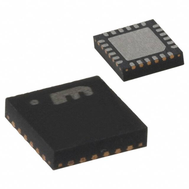


 工商网监
湘ICP备2023018690号
工商网监
湘ICP备2023018690号
