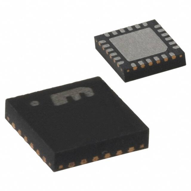
MIC3263
Six-Channel WLED Driver for
Backlighting Applications with
Flicker-Free Dimming
General Description
Features
The MIC3263 is a high-efficiency Pulse Width Modulation
(PWM) boost switching regulator that is optimized for
constant-current WLED driver backlighting applications.
The MIC3263 drives six channels of up to ten WLEDs per
channel. Each channel is matched in current to within ±3%
for constant brightness across the screen and can be
programmed from 15mA to 30mA.
The MIC3263 provides a very flexible dimming control
scheme with better accuracy and noise immunity. The
dimming frequency can be set to any value between
100Hz and 20kHz by an external resistor. The dimming
ratio is determined by the duty cycle of a dimming ratio
control input signal and can be set to one of 16 levels with
a minimum ratio of 1%.The LED dimming current is set by
an external resistor to allow programming of LED current
between 15mA and 30mA.
The dimming ratio of the MIC3263 is fixed to 16 log levels
to better match the sensitivity of the human eye. Each of
the dimming levels has hysteresis to avoid skipping
between levels and allow for high noise immunity.
The MIC3263 has a programmable PWM switching
frequency from 400 KHz to 1.8 MHz to allow small inductor
sizes. The 6V to 40V wide input voltage range of MIC3263
allows direct operation from 6V or high cell count Li-Ion
batteries commonly found in notebook computers.
The MIC3263 is available in a low-profile 24-pin 4mm x
4mm MLF® package and has a junction temperature
range of −40°C to +125°C.
Data sheets and support documentation can be found on
Micrel’s web site at: www.micrel.com.
•
•
•
•
•
•
•
•
•
•
•
•
•
•
•
•
6V to 40V wide input voltage range
Drives 6 channels of up to 10 white LEDs
Programmable WLED current from 15mA to 30mA
Highly reliable operation with open and short LEDs
Accurate 16 dimming log levels sets the dimming ratio
from 1% to 100%
Flicker-Free Dimming filters the jitter from the dimming
control input signal and eliminates dimming flicker
Allows external dimming control
Accurate LED channel current matching ±3%
Accurate initial LED current setting ±2%
Programmable switching frequency from 400kHz to
1.8MHz
High efficiency up to 90%
Low ( 1.2V
All Channels
On
2 LEDs Short
in Same
Channel
NO
1.2 < IO < 7.5
All Channels
On
More Than 2
LEDs Short
in Same
Channels
YES
IO > 7.5V
1 Channel
Off; 5
Channels On
1 LED Opens
in Channel 1
YES
IO < 0.5V
1 Channel
Off; 5
Channels On
2 or 3
Channels
Open LEDs
YES
IO < 0.5V
3 Channels
Off; 3
Channels On
4 or More
Channels
Open
YES
IO < 0.5V
4 Channels
Off; 2
Channels On
All Channels
Open
YES
OVP
Threshold
Exceeded
OVP
Triggered
VOUT Shorted
YES
Current Limit
Exceeded
Output
Current is
Limited
Table 1. Fault Summary
Power-On Sequence
VIN needs to be present before PWM pulses are applied to
the DRC pin. Some channels may not turn on if the power
up sequence isn’t followed. This is because the circuits
that monitor the IO pins may see transients during the turn
on-time and may interpret voltage spikes during turn on as
a fault, preventing that channel from turning on. When a
channel is off, its IO pin is at high impedance.
It is best to follow the sequence:
1. VIN
2. PWM dimming at DRC
3. Enable high
January 2010
14
M9999-012110
�Micrel, Inc.
Pin Descriptions
MIC3263
Use the following equations to determine the value for
RDFS:
FSW
Sets the boost switching frequency. Connect a resistor
from FSW to GND to set the switching frequency between
400kHz and 1.8MHz. Use the following equations to select
RFSW:
RSLP
The boost section is a peak current mode typology and
needs slope compensation to eliminate sub-harmonic
oscillation (see “Slope Compensation”).
OVPS
This is a virtual ground of the resistor divider feedback
network in the boost stage. At turn on, a switch connects
this node-to-ground. When the part is disabled the switch
will open and disconnects the feedback resistor network
from ground. This eliminates current draw from VIN by the
boost resistor divider network.
OVP
This is the over-voltage protection monitor. Also this is the
feedback signal that connects to the error amp input.
MODE
This selects the internal PWM dimming frequency range.
When mode is low the PWM dimming frequency range is
100Hz to 2kHz. When mode is high the PWMD frequency
range is 1.5kHz to 20kHz. Mode is high selects High
Frequency (HF) mode; Mode is low selects Low
Frequency (LF) mode.
RDFS(kΩ) = −335 × fDIM(kHz) + 433 (LF Mode)
Example:
For a dimming frequency of 10kHz, use the HF Mode:
RDFS(kΩ) = −20 × 10 + 432 = 232kΩ in HF Mode
For 1kHz, use LF Mode:
RDFS(kΩ) = −335 × 1 + 433 = 98kΩ in LF Mode
Use the closest standard value.
400
350
300
250
200
150
100
50
0
0
2.5
5
7.5
10
12.5
15
17.5
20
22.5
Dimming Frequency (kHz)
Figure 5. RDFS vs. Dimming Frequency in HF Mode
DFS
DFS stands for Dimming Frequency Select. The dimming
frequency of the LEDs is different than the input dimming
frequency at the DRC input. The MIC3263 uses an internal
dimming frequency. This internal dimming frequency is
programmable by an external resistor to ground RDFS.
For direct dimming control, connect DFS to VDD and use
the MODE pin for the input dimming pulse. This method by
passes the internal dimming control and allows for
dimming control by the external PWM pulse.
When using internal dimming the range is determined by
the MODE pin and the actual frequency is determined by
RDFS. Connect a resistor to ground to select a dimming
frequency.
January 2010
RDFS(in kΩ) = -20*Dimming Frequency (in kHz) + 432
450
RDF S (kΩ)
RFSW (kΩ) ≈ 500 − 0.3 × fSW(kHz)
RDFS(kΩ) = −20 × fDIM(kHz) + 432 (HF Mode)
RDFS(kΩ) = -335*Dim m ing Frequency (in kHz) + 433
500
RDFS(kΩ)
400
300
200
100
0
0
0.2
0.4
0.6
0.8
1
1.2
1.4
Dim m ing Frequency (kHz)
Figure 6. RDFS vs. Dimming Frequency in LF Mode
15
M9999-012110
�Micrel, Inc.
The input frequency to the DRC pin can be 100Hz to
40kHz and the internal dimming frequency DR will be
determined by RDFS.
The duty cycle of the input frequency at DRC is converted
according to Table 2 for the actual dimming duty cycle.
For direct dimming control, connect DFS to VDD and use
the MODE pin for the input dimming pulse. This method by
passes the internal dimming control and allows for
dimming control by the external PWM.
DFS Filter
In addition to the RDFS resistor-to-ground at the DFS pin, a
series RC filter is required when operating at dimming
frequencies below 1kHz. The reason is that the DFS pin is
the output of a transconductance differential amplifier. The
differential amplifier has a high-frequency pole.
At low dimming frequencies of around 1kHz RDFS is high
around 100kΩ and the differential amplifier pole produces
a phase shift that can cause instabilities in the DFS
control.
Therefore, a RC filter is required to compensate for the
lagging phase shift created by the pole by adding a zero
and therefore, a phase lead at the DFS pin. Use a 4kΩ
resistor in series with a 2.2nF ceramic capacitor. When
using a dimming frequency of 2 kHz or less. The filter has
no ill effect at higher dimming frequencies.
COMP
Connect a capacitor and resistor to ground to compensate
the boost stage.
DRC
Dimming Ratio Control (DRC) is an input PWM dimming
control. The MIC3263 converts this to one of sixteen
dimming ratios that is used to dim the LEDs. The dimming
ratio is built on a log scale.
CINT
CINT integrates the DRC input pulse. For a PWM frequency
range of around 1kHz use 100nF. For a PWM frequency
range of around 20kHz pulse, use 10nF. For a PWM
frequency range of around 100Hz pulse use 1μF.
ISET
Set the LED current of all six channels by this resistor. Use
2kΩ for 30mA and 3kΩ for 20mA. The RISET is inversely
proportional to ILED. Use the following equation to find
RISET:
60
RISET =
Ω
ILED
January 2010
MIC3263
For the best current matching accuracy design for an ILED
current of 15mA to 30mA.
CRV
Use a 2.2μF capacitor at the CRV pin. This is used as the
reference voltage of the boost stage. The CRV capacitor is
continually being charged or discharged in order to keep
VOUT at the right level (refer to Functional Diagram
illustration). CRV will be charged to keep the IO’s at about
1.2V.
IO1─IO6
These are the connections to the linear-mode current
amplifier in each channel. Connect the cathode end of the
LED channels to these pins. The control loop will keep this
at about 1.2V. 1.2V insures that the current amplifier is in
the linear region and therefore can regulate the LED
current.
In cases where there are a different number of LEDs in a
channel, the V(IO) of the channel with the fewest LEDs will
have a higher V(IO). V(IO) can be as high as 7.5V before
the fault monitoring circuits will sense that channel as a
short to VOUT.
When there are a different number of LEDs in a channel
the IO voltage will be higher in the channels that have less
LEDs in order to keep the LEDs biased correctly. A
difference of up to 7.5V between channels can occur
because of this. If the circuits that monitors the IO pins
sees a fault, that channel will turn off and that channel’s IO
pin will be at high impedance. An off channel’s IO pin will
be near or below the booster output voltage. On a channel
that has a shorted LED, that channel’s IO voltage will
increase to keep correct voltage drops on the other series
LEDs. It is best to use equal number of LEDs in each
channel but there will always be differences in the LEDs
voltage drops so all IOs will not have the exact same
voltage. Each channel has its own monitoring circuit
monitoring the IO1─IO6 pins. If any V(IO) drops below
0.5V (if an LED opens), that channel is turned off and the
other channels are unaffected. If any IO goes about 7.5V
(if several LEDs short to VOUT), that channel is turned off
and the other channels are unaffected.
VSW
This is the boost-stage switch node, the collector of the
internal power switch.
EN
Connect EN high to enable the part, low to disable. Do not
leave the EN pin floating.
VIN
Supply voltage to the part (6V–40V).
16
M9999-012110
�Micrel, Inc.
MIC3263
VDD
This is the output of the internal LDO regulator. Connect a
10μF ceramic capacitor to this pin.
PWM Dimming
The duty cycle of the PWM pulse applied to the DRC input
is converted to 16 log levels. This logarithmic dimming is a
unique feature of the MIC3263 which better matches the
sensitivity of the human eye compared to linear dimming.
The DRC duty-cycle to DR duty-cycle conversion is shown
in Table 2.
N
DRC Duty
Cycle
PWM Dimming Ratio (DR)
(N 1) / 7
DR = 10 −
%
%
0
6.25
12.5
18.75
25
31.25
37.5
43.75
50
56.25
62.5
68.75
75
81.25
87.5
93.75
0
1.0
1.4
1.9
2.7
3.7
5.2
7.2
10
14
19
27
37
52
72
100
0
1
2
3
4
5
6
7
8
9
10
11
12
13
14
15
Table 2. Dimming Ratio
To avoid skipping between dimming levels, the MIC3263
uses Flicker-Free Dimming control. This technique uses a
digital filter and hysteresis on the DRC pulse to provide a
clean DR output. The digital filter has a 0.1μF capacitor on
the CINT pin to average the duty cycles of the PWM
pulses. The averaged duty cycle has to be 4.16% higher
than the nominal value before moving to the next dimming
level as shown in Figure 7. Likewise, to move the previous
dimming level the duty cycle has to be −4.16% lower than
the nominal. To prevent flicker the duty-cycle hysteresis is
set a 2%.
January 2010
Figure 7. Duty-Cycle Thresholds and Hysteresis
PWM Dimming Limits
The minimum pulse width of the PWM Dim is determined
by the PWM Dimming frequency and the L and C used in
the boost stages output filter. At low-PWM Dimming
frequencies, higher dimming ratios can be achieved:
T
Dim Ratio = PWMD
T
LEDON
Figure 8. PWM Dimming Ratio
Consider that the human eye will perceive light flicker at a
PWM dimming frequency below 100Hz. At 100Hz the time
between pulses is 10μs. If the PWM dimming minimum
pulse width is 5μs, then:
Dim Ratio =
10ms
5μs
= 2000/1
If high dimming ratios are required, a lower dimming
frequency is required. During each DR pulse, the inductor
current has to ramp up to it steady state value to generate
the necessary boost output voltage in order for the full
programmed LED current to flow in the LED channels. The
smaller the inductance value the faster this time is and a
narrower PWM dimming pulse can be achieved. But
smaller inductance means higher ripple current.
17
M9999-012110
�Micrel, Inc.
MIC3263
Figure 9 shows the waveforms during PWM dimming
pulses. The DRC duty cycle is 75% and therefore the
dimming ratio (DR) is 37%. Ch1 is the switch node. Ch2 is
the sum of all six ILED channels. Figure 9 shows the boost
converter is OFF (not switching) between PWM dimming
pulses.
Figure 9. PWM Dimming Pulses
(Ch1 Switch Node; Ch2 is the ILED Total)
Direct Dimming
For direct dimming control connect DFS to VDD and use
the MODE pin for the dimming pulse. This method will
bypass the internal dimming control and allows for
dimming control by the external PWM Dimming pulse (see
Figure 9).
January 2010
Figure 10. Direct Dimming Control
Boost Stage
A current-mode control is easier to compensate than
voltage mode control, thus allowing for a less complex
control loop stability design. An error amplifier amplifies
the difference between the feedback voltage and the
voltage on the CRV capacitor. This amplified error signal is
called the VCONTROL. A PWM comparator compares the
output of the error amp (VCONTROL) to the sum of inductor
current and slope compensation currents. When the
current sums reach VCONTROL, the PWM pulse is terminated
and the boost power switch is turned off. A portion of the
energy stored in the inductor flows into the output
capacitor.
18
M9999-012110
�Micrel, Inc.
MIC3263
Slope Compensation
The boost stage uses peak current mode and requires
slope compensation. Slope compensation is required to
maintain internal stability of the boost stage across all duty
cycles and to prevent any unstable oscillations. The
MIC3263 uses a combination of internal slope
compensation and a additional slope compensation that is
set by an external resistor, RSLP. The ability to set the
proper slope compensation through the use of a single
external component results in design flexibility. This slope
compensation resistor, RSLP, can be calculated as
follows:
Figure 11. Boost Stage
RSLP =
VOUT(MAX) - L ×Fsw
8.64 ×10⁻⁶ × V
IN(MIN)
The operating duty cycle can be calculated using the
equation provided below:
D=
(VOUT - eff × VIN )
VOUT
and D′ = 1 − D
Find L using the following equation:
L=
where VIN(MAX) and VOUT(MAX) can be selected to system
specifications. The lowest value of RSLP should be 15kΩ.
Calculate RSLP using the lowest VIN and maximum VOUT
the system will operate.
Example: For these operating conditions:
VIN(MIN) = 12V, VOUT(MAX) = 32V, L = 22μH,
FSW = 1MHz
VIN ×D
IL_PP ×Fsw
RSLP =
IL_PP is the inductor peak-to-peak ripple current.
Use a IL_PP of 20% to 40% of the total load current. FSW is
the boost switching frequency.
Output Capacitor
In a boost converter, to find the COUT for a given VOUT
ripple use the following calculation:
COUT =
32V - 22μH×1Mhz
= 96.5kΩ
8.64 ×10-6 ×12V
Use the next highest standard value.
Table 3 compiles and lists RSLP values for one set of
operating conditions. Select RSLP for VIN_MIN and VO_MAX.
ILEDtotal ×D
VRIPPLE × Fsw
VRIPPLE can usually be kept below 50mV:
ILED_TOTAL = 6 × 30mA = 180mA
In the MIC3263, the LED current in each channel is
individually regulated by that channels current amplifier
(linear current regulator). These current regulators are fast
enough to follow the boost output voltage ripple and to
keep the LED ripple currents much lower than COUT can
filter the output ripple voltage.
January 2010
19
M9999-012110
�Micrel, Inc.
MIC3263
From the small signal block diagram the loop transfer
function is:
VIN = 12V, VOUT = 32V
F(kHz)
400
500
600
700
800
900
1000
1100
1200
1300
1400
1500
1600
1700
1800
8.2μH
10μH
22μH
RSLP
RSLP
RSLP
2.77E+05
2.69E+05
2.61E+05
2.53E+05
2.45E+05
2.37E+05
2.30E+05
2.22E+05
2.14E+05
2.06E+05
1.98E+05
1.90E+05
1.82E+05
1.74E+05
1.66E+05
2.70E+05
2.60E+05
2.51E+05
2.41E+05
2.31E+05
2.22E+05
2.12E+05
2.03E+05
1.93E+05
1.83E+05
1.74E+05
1.64E+05
1.54E+05
1.45E+05
1.35E+05
2.24E+05
2.03E+05
1.81E+05
1.60E+05
1.39E+05
1.18E+05
96451
75231
54012
32793
15000
15000
15000
15000
15000
Figure 13. Simplified Voltage Control Loop
Equation 2:
T(s) = Gea(s) × GVC(s) × H(s)
where:
H(s) =
Table 3. RSLC Values
Boost Compensation
Current-mode control simplifies the compensation. In
current mode the double pole created by the output L and
C is reduced to a single pole. The explanation for this is
beyond the scope of this data sheet, but it can be thought
because the inductor current becomes a constant current
source and can’t act to change phase.
VCRV
and
VOUT
⎛
⎛
⎝
⎝
Gea (s) = gm ⎜ Z o II ⎜ R COMP +
⎞⎞
⎟⎟
sCCOMP ⎠ ⎠
1
Equation 3:
Gvc (s) =
VOUT ( s )
VCONTROL ( s )
⎛
⎞
sL
⎜1⎟
2
⎜
⎟
⎛ 1 ⎞ ⎛ D'RLOAD ⎞ ⎝ D' RLOAD ⎠
= ⎜ ⎟⎜
⎟
2
⎝ Ri ⎠ ⎝
⎠ ⎛ 1+ sRLOADCOUT ⎞
⎜
⎟
2
⎝
⎠
Figure 12. MIC3263 Current-Mode Loop Diagram
where RLOAD =
VOUT
IOUT
and Ri = Ai × Rcs = 0.4Ω .
Ai = 20
RCS = 0.02Ω
AI and RCS are quantities that are internal to the MIC3263.
The equation for GVC(S) is a theoretical model and should
give an approximate idea of where the poles and zeros are
located.
January 2010
20
M9999-012110
�Micrel, Inc.
MIC3263
Equation 3 shows that s =
2
D' RLOAD
L
is a right-half plane
Error Amp
The error amp is a gm type and the gain – GEA(S) – is:
zero (fRHPZ):
Equation 5:
Equation 4:
⎛
⎛
⎝
⎝
Gea (s) = gm ⎜ Z o II ⎜ R COMP +
RHP Zero→ fRHPZ =
2
D' RLOAD
2πL
The loop bandwidth should be about 1/10 of the fRHPZ to
ensure stability. From Equation 3, it is shown that there is
only the single pole due to RLOADCOUT. This greatly
simplifies the compensation.
One needs only to get a bode plot of the transfer function
of the control to output GVC(S) with a network analyzer.
To measure GVC(S), tie CRV to a DC voltage source. Tie
CRV to the steady state voltage that CRV will operate
usually between 1V and 2.4V. By connecting CRV to a
constant DC voltage, this effectively opens the CRV
control loop and allows the measurement of the boost
control loop. GVC(S) can be calculated with a computer
using the above equation. From the bode plot of GVC(S)
find what the gain of GVC(s) is at 1/10 of fRHPZ or less. Next
design the error amp gain GEA(s) so the loop gain at the
cross over frequency T(fCO) is 0db where fCO =1/10 of fRHPZ
or lower.
gm = 0.056mA/V and ZO = 5MΩ. The error amplifier zero is
1
f
=
. Set the fCO at the mid band
Zero 2πR
C
COMP
COMP
where GEA(fCO) = gm × RCOMP. At fZERO × 10 the phase boost
is near its maximum.
40
Figure 15. Internal Error Amp and External Compensation
Midband Gain
20
Gain (db) phase (deg)
⎞⎞
⎟⎟
sCCOMP ⎠ ⎠
1
Example 1
Conditions: VIN = 12V, VOUT = 29V, IOUT = 0.18A, L = 22μH,
COUT = 4.7μF RLOAD = VOUT/IOUT = 161Ω. When VCRV =
1.8V, the fRHPZ is:
0
Fzero
-20
-40
-60
Gain
Phase
-80
fRHPZ =
-100
1.E+02
1.E+03
1.E+04
1.E+05
2
D' RLOAD
2πL
= 162kHz
1.E+06
Freq
Figure 16 shows a plot of:
Figure 14. Error Amp Transfer Function
Gvc (s) =
VOUT ( s )
VCONTROL ( s )
⎛
⎞
sL
⎜1⎟
2
⎜
⎟
⎛ 1 ⎞ ⎛ D'RLOAD ⎞ ⎝ D' RLOAD ⎠
= ⎜ ⎟⎜
⎟
2
⎝ Ri ⎠ ⎝
⎠ ⎛1+ sRLOADCOUT ⎞
⎜
⎟
2
⎝
⎠
January 2010
21
M9999-012110
�Micrel, Inc.
MIC3263
This example illustrates the RHPZ at 162kHz. Figure 16
details the −90° phase shift due to the RHPZ.
100
Therefore R4 = 15kΩ. Next set the error amplifier’s zero at
about 5kHz. Therefore C2 = 2.2nF. The location of the
fZERO affects the phase boost in the loop transfer function.
If fZERO were closer to 16kHz the phase boost would be
less and vise versa.
26db
50
0
Midband Gain
20
Gain (db) phase (deg)
Gain (db) phase (deg)
40
-50
-100
Gain
Phase
-150
0
Fzero
-20
-40
-60
Gain
Phase
-80
-200
1.E+02
1.E+04
1.E+03
1.E+05
1.E+06
-100
1.E+02
Freq
1.E+03
1.E+04
1.E+05
1.E+06
Freq
Figure 16. Control-to-Output Gain (GVC)
Figure 17. Error Amp Gain and Phase (in Example 1)
The goal is to make the loop transfer function T(fCO)
crossover well before the RHPZ.
fRHPZ
or less; chose fco = 16kHz .
10
From the plot and or calculation, the magnitude of:---
Chose a fco =
100
Gain (db) phase (deg)
80
Gvc (16kHz) = 26db
⎛ 1.8V ⎞
⎟ = -24db
⎝ 29V ⎠
H(s) = 20Log ⎜
60
40
20
0
Gain
-20
Fco=1.6kHz
Phase
From:
-40
1.E+02
T(s) = Gea (s) * Gvc (s) * H(s)
1.E+03
1.E+04
1.E+05
1.E+06
Freq
T(16kHz) = Gea (16kHz) + 26db - 24db = 0
Figure 18. Loop Gain and Phase (in Example 1)
Gea (16kHz) = -2db → 0.8v/v
(
)
0.8 = gm Z o II R 4 ≅ gm * R 4
January 2010
22
M9999-012110
�Micrel, Inc.
MIC3263
Design Procedure for a LED Driver
Symbol
Input
VIN
IIN
Output
LEDs
Chs
VF
VIO
VOUT
ILED/ch
IOUT
POUT
DIM IN
FDIM
OVP
FSW
eff
VDIODE
Parameter
Minimum
Nominal
Maximum
Units
8
12
14
V
8/Channel
6
3.4
1.1
28
30
8/Channel
6
3.6
1.2
30
30
8/Channel
6
4.0
2
34
30
0.18
6.2
100
Input Voltage
Input Current
Number of LEDs
Number of Channels
Forward Voltage of LED
Voltage Drop at the IO Pin
Output Voltage
LED Current/Channel
Output Power
PWM Dimming
Dimming Frequency (internal)
Output Over-Voltage Protection
Switching Frequency
Efficiency
Forward Drop of Schottky Diode
1
5
40
80
V
mA
A
W
%
kHz
V
MHz
%
V
Let VCRV = 2.2V therefore:
Design Example
In this example, a boost six-channel LED driver
operating off a 12V input is being designed. This design
has been created to drive six channels of eight
LEDs/channels for a total of 48 LEDs. The LED current
will be set at 30mA. One is designing for 80% minimum
efficiency at a switching frequency of 1MHz.
For 34V out:
Let R2=150k,
R1 =
VCRV × R2
VOUT - VCRV
=
2.2V × 150kΩ
34V - 2.2V
= 10.4kΩ
Use the closest standard value of 10.5kΩ.
Therefore:
VOVP = 2.4* (R2+R2)/R1 = 40V
V
×R2
1.8V ×150kΩ
R1= CRV
=
= 8.39kΩ
VOUT - VCRV
34V -1.8V
Select RISET for a Given ILED
Therefore: VOVP= 2.4* (R2+R2)/R1=45V. 45V is too high,
meaning VCRV has to operate at a higher voltage than
1.8V. The CRV loop will charge the CRV capacitor to the
necessary voltage to regulate.
January 2010
1
85
0.5
Channels
V
RISET =
60
ILED
Ω=
60
= 2kΩ
30mA
Use 2kΩ for RISET (R9)
23
M9999-012110
�Micrel, Inc.
MIC3263
Switching Frequency Set RFSW
To find the value of RFSW use the following equation:
Inductor Selection
First calculate the RMS input current (nominal, minimum,
and maximum) for the system given the operating
conditions listed in the design example table. The
minimum value of the RMS input current is necessary to
ensure proper operation. Using Equation 7, the following
values have been calculated:
RFSW(kΩ) ≈ 500 − 0.3 × fSW(kHz)
RFSW(kΩ) ≈ 500 − 0.3 × (1000) = 200kΩ
Equation 7:
Use 200kHz for RFSW (R5).
Dimming Frequency Select Resistor RDFS
FDIM is 5kHz therefore HF mode is used. Connect MODE
to VDD. To find RDFS (R8) use the following equation:
IIN_RMS(MAX) =
IIN_RMS(NOM) =
RDFS(in kΩ) = 432 − 20 × FDIM(in kHz)
= 432 − 20 × 10 = 232(kΩ)
IIN_RMS(MIN) =
The input frequency to the DRC pin can be 100Hz to
40kHz and the internal dimming frequency DR will
always be 5kHz.
The duty cycle of the input frequency at DRC is
converted according to Table 2 for the actual dimming
duty cycle.
Since the dimming frequency is high the filter R6 and C6
is not necessary. They may be used with no ill effect.
DMAX =
DMIN =
OUT(NOM)
(V
- eff × VIN(NOM)
VOUT(NOM)
OUT(MAX)
- eff × VIN(MAX)
OUT(MAX)
- eff × VIN(MAX)
VOUT(NOM) × IOUT(NOM)
eff × VIN(NOM)
VOUT(MAX) × IOUT(MAX)
eff × VIN(MIN)
= 0.53A (RMS)
= 0.9A (RMS)
IL_PP(MAX) = 0.40 × IIN_RMS(MAX) = 0.4 × 0.9 = 0.36APP
There is a trade off between the inductor value and the
minimum PWM dimming pulse. The larger the inductor,
the longer the PWM dimming pulse time will be. Due to
this, the percentage of the ripple current may be limited
by the required PWM dimming pulse. Also, the internal
current amplifiers will attenuate the LED ripple current by
more than a magnitude. It is recommended to operate in
the continuous conduction mode. The value of “L” in
Equation 8 represents Continuous Conduction Mode.
)
)
Equation 8:
VOUT(MAX)
(V
= 0.43A (RMS)
Selecting the inductor current (peak-to-peak) IL_PP to be
between 20% to 50% of IIN_RMS(max), in this case 40%, we
obtain:
Equation 6:
(V
eff × VIN(MAX)
IOUT is the same as ILED total
Operating Duty Cycle
The operating duty cycle can be calculated using
Equation 6.
DNOM =
VOUT(MIN) × IOUT(MIN)
)
L=
VOUT(MAX)
VIN × D
IL_PP × FSW
Therefore DNOM = 66%, DMAX = 80% and DMIN = 58%.
January 2010
24
M9999-012110
�Micrel, Inc.
MIC3263
Using the nominal values, one gets:
L=
12V × 0.66
0.36A × 1MHz
A Coilcraft # DO3316P-223ML is used in this example.
Its DCR is 85 mΩ, ISAT =2.6A.
PINDUCTOR(MAX) = 0.92 × 85 mΩ = 67mW
= 22μH
Output Capacitor
In this LED driver application, the ILED ripple current is a
more important factor compared to that of the output
ripple voltage (although the two are directly related). To
find the COUT for a required ILED ripple use the following
calculation:
For an output ripple ILED(RIPPLE) = 20mA.
If not a standard value, use the next higher standard
value. Select the standard inductor value of 22µH.
Going back and calculating the actual ripple current
gives:
IL_PP =
VIN(NOM) × DNOM
L × FSW
=
12V × 0.66
22μH × 1MHz
= 0.36APP
Equation 12:
The average input current is different than the RMS input
current because of the ripple current. If the ripple current
is low, then the average input current nearly equals the
RMS input current. In the case where the average input
current is different than the RMS, Equation 9 shows the
following:
COUT =
IIN_AVE(MAX) =
ILED(total) = 6 × 30mA = 180mA
(IIN_RMS(MAX) )
(0.9)
2
2 (IIN_PP )
12
(0.36)
12
COUT =
2
0.18A × 0.76
50mV × 1Mhz
= 2.7μF
Use 2.7µF or higher.
The amount that COUT will discharge depends upon the
time between PWM Dimming pluses and the size of the
output capacitor. At the next PWM Dimming pulse COUT
has to be charged up to the full output voltage VOUT
before the desired LED current flows.
2
≈ 0.9A
The Maximum Peak input current IL_PK can found using
Equation 10:
Input Capacitor
The input capacitor is shown in the Typical Application.
For superior performance, ceramic capacitors should be
used because of their low Equivalent Series Resistance
(ESR). The input capacitor CIN ripple current is equal to
the ripple in the inductor. The ripple voltage across the
input capacitor, is the ESR of CIN times the inductor
ripple. The input capacitor will also bypass the EMI
generated by the converter as well as any voltage spikes
generated by the inductance of the input line. For a
required VIN(RIPPLE).
Equation 10:
IL_PK(MAX) = IIN_AVE(MAX) + 0.5 ×IL_PP(MAX) = 1.0A
The saturation current (ISAT) at the highest operating
temperature the inductor must be rated higher than this.
The power dissipated in the inductor is:
Equation 11:
PINDUCTOR(max) = IIN_RMS(MAX)2 × DCR
Equation 13:
CIN =
January 2010
VRipple × Fsw
VRIPPLE can usually be kept below 50mV:
Equation 9:
IIN_AVE(MAX) =
ILED(total) × D
25
IIN_PP
8 × VIN(RIPPLE) × FSW
=
(0.36A )
8 × 50mV × 1MHz
= 0.8μF
M9999-012110
�Micrel, Inc.
MIC3263
This is the minimum value that should be used. To
protect the IC from inductive spikes or any overshoot, a
larger value of input capacitance may be required. Use
2.2µF or higher as a good safe min.
Equation 17:
PWR SW_ON( MAX) = ISW_RMS(MAX) × VCE_ON_RMS (MAX)
⎛
Rectifier Diode Selection
A Schottky diode is best used here because of the lower
forward voltage and the low reverse recovery time. The
voltage stress on the diode is the maximum VOUT and
therefore, a diode with a higher rating than maximum
VOUT should be used. An 80% de-rating is recommended
here as well.
ISW_RMS(MAX) = D(MAX) ×⎜⎜ IIN_AVE(MAX)2 +
(IIN_PP )2 ⎞⎟
⎜
⎝
12
⎟
⎟
⎠
≈ D(MAX) × IIN_AVE(MAX)
VCE_ON_RMS (MAX) = D(MAX) × VCE_ON( MAX)
PWR SW_ON( MAX) = D(MAX) × IAVE(MAX) × VCE_ON (MAX)
Equation 14:
PWR SW_ON( MAX) = 0.8 × 0.9A × 0.5V = 0.36W
Equation 18:
IDIODE_(MAX) = IOUT(MAX) = 0.18A
PWR SW_SWITCHING (MAX) = VOUT(MAX) × IIN_AVE(MAX) × tsw × Fsw
Equation 15:
tsw ≈ 20ns is the internal power switch on an off
transition time
PDIODE(MAX) ≈ VDIODE × IDIODE_(MAX)
PWRSW_SWITCHING (MAX) = 34V ×0.9 × 20ns ×1MHz = 0.61W
A SK34A is used in this example, it’s VDIODE is 0.5V.
Therefore:
PDIODE(MAX) ≈ 0.5V × 0.18A≈ 0.09W
PMIC3263(MAX) = 14V × 35mA + 0.97 = 1.46W
MIC3263 Power Losses
To find the power losses in the MIC3263: There is about
25mA to 35mA input from VIN into the VDD pin. The
internal bipolar power switch has an VCE(ON MAX) of about
0.5V.
Snubber
If a high-frequency ringing is present at VSW, a snubber
may be needed. A snubber is a damping resistor in
series with a DC blocking capacitor in parallel with the
power switch. When the power switch turns off, the drain
to source capacitance and parasitic inductance will
cause a high frequency ringing at the switch node. A
snubber circuit as shown in the application schematics
may be required if ringing is present at the switch node.
A critically damped circuit at the switch node is where R
equals the characteristic impedance of the switch node.
VCE(ON MAX) ≈ 0.5V
Equation 16:
PMIC3263(MAX) = VIN(MAX) × 35mA + PWRSW(MAX)
Equation 18:
Where PWRSW(MAX) is the power loss of the internal
bipolar power switch. The power switch power losses
are the sum of the on-time losses; PWRSW(MAX) and the
switching losses: PWRSW(SWITCHING MAX).
R SNUBBER =
LPARISITIC
CDS
PWRSW(MAX) = PWRSW(MAX) + PWRSW(SWITCHING MAX)
January 2010
26
M9999-012110
�Micrel, Inc.
MIC3263
The explanation of the method to find the best R
snubber is beyond the scope of this data sheet. Use
RSNUBBER ≈ 2Ω ½ W and CSNUBBER ≈ 470pF to 1000pF. If
a snubber is used, the power dissipation in the RSNUBBER
is:
OVP
The output voltage that the OVP will trigger is set
according to Equation 19. Using the values for this
example gives a max output voltage of:
RSNUBBER = CSNUBBER × VOUT2 × FSW
Equation 19:
VOVP= 2.4× (R2+R2)/R1=40V
PSNUBBER = 470pF × 34V2 × 1MHz = 0.54W
RSLP
To find RSLP use Equation 1 (which is repeated here):
Use the minimum VIN and the maximum VOUT.
Table 2 illustrates the power losses in the Design
Example.
Description
Value
Power Loss in the L
0.069W
Power Loss in the Schottky Diode
0.09W
MIC3263 Power Loss
1.46W
Maximum Total Losses
1.62W
Minimum Efficiency
RSLP =
In this example:
80%
RSLP =
Table 2. Major Power Losses
January 2010
VOUT(MAX) - L × Fsw
-6
8.64 × 10 × VIN(MIN)
27
34 - 22μH × 1Mhz
= 174kΩ
-6
8.64 × 10 × 8
M9999-012110
�Micrel, Inc.
MIC3263
Evaluation Board Schematic
January 2010
28
M9999-012110
�Micrel, Inc.
MIC3263
Bill of Materials
Item
Part Number
Manufacturer
C1
(1)
0603ZC222KAT2A
AVX
C1608X7R1H222K
TDK(2)
muRata
C5750X7R1H106M
TDK(2)
22205C106KAZ2A
AVX(1)
GRM21BR71A106KE51L
muRata(3)
0805ZD106KAT2A
AVX(1)
0603YC104KAT2A
AVX(1)
C1608X7R1C104K
TDK(2)
C5
muRata
0603ZD225KAT2A
AVX(1)
GRM188R61A225KE34D
muRata(3)
L1
R1
TDK
MCC(4)
B349LA-13
Diode, Inc. (5)
DO3316P-223ML
Coilcraft(6)
CRCW0603150KFKEA
10μF, 50V, X7R, 2220
2
10μF, 10V, 0805
1
0.1μF, 16V, X7R, 0603
1
2.2μF, 10V, X5R, 0603
1
Schottky 3A, 40V (SMA)
1
(2)
SK34A
D1
2
(3)
GRM188R71C104K
C1608X5R1A225K
2200pF, 10V, X7R, 0603
(3)
GRM188R71H222K
C3, C8
C7
Qty.
OPEN
C2, C6
C4
Description
22μH, 2.6A
1
(7)
150k
2
(7)
Vishay Dale
R2
CRCW060310K0FKEA
Vishay Dale
10k
1
R3
CRCW0603110KKFKEA
Vishay Dale(7)
110k (RSLP)
1
R4
CRCW060315K0FKEA
Vishay Dale(7)
15.0k, 0603 (RCOMP)
1
CRCW060340K2FKEA
(7)
4.02k
(7)
R6
Vishay Dale
R5
CRCW0603200KFKEA
Vishay Dale
200k
1
R7
CRCW0603100KFKEA.
Vishay Dale(7)
100k
1
CRCW060326K7FKEA
(7)
97.6k
1
(7)
Vishay Dale
2k
1
Micrel, Inc.(8)
Six-Channel WLED Driver for Backlighting Applications
1
R8
R9
CRCW06032K00FKEA.
U1
MIC3263YML
Vishay Dale
Notes:
1. AVX: www.avx.com.
2. TDK: www.tdk.com.
3. Murata Tel: www.murata.com.
4. MCC: www.mccsemi.com.
5. Diode, Inc.: www.diodes.com.
6. Coilcraft: www.coilcraft.com.
7. Vishay: www.vishay.com.
8. Micrel, Inc.: www.micrel.com.
January 2010
29
M9999-012110
�Micrel, Inc.
MIC3263
Evaluation Board PCB Layout
January 2010
30
M9999-012110
�Micrel, Inc.
MIC3263
Package Information
24-Pin 4mm x 4mm (MLF®)
January 2010
31
M9999-012110
�Micrel, Inc.
MIC3263
Recommended Land Pattern
MICREL, INC. 2180 FORTUNE DRIVE SAN JOSE, CA 95131 USA
TEL +1 (408) 944-0800 FAX +1 (408) 474-1000 WEB http://www.micrel.com
The information furnished by Micrel in this data sheet is believed to be accurate and reliable. However, no responsibility is assumed by Micrel for its
use. Micrel reserves the right to change circuitry and specifications at any time without notification to the customer.
Micrel Products are not designed or authorized for use as components in life support appliances, devices or systems where malfunction of a product
can reasonably be expected to result in personal injury. Life support devices or systems are devices or systems that (a) are intended for surgical implant
into the body or (b) support or sustain life, and whose failure to perform can be reasonably expected to result in a significant injury to the user. A
Purchaser’s use or sale of Micrel Products for use in life support appliances, devices or systems is a Purchaser’s own risk and Purchaser agrees to fully
indemnify Micrel for any damages resulting from such use or sale.
© 2010 Micrel, Incorporated.
January 2010
32
M9999-012110
�